WO2012014642A1 - ゲートスタック形成方法 - Google Patents
ゲートスタック形成方法 Download PDFInfo
- Publication number
- WO2012014642A1 WO2012014642A1 PCT/JP2011/065430 JP2011065430W WO2012014642A1 WO 2012014642 A1 WO2012014642 A1 WO 2012014642A1 JP 2011065430 W JP2011065430 W JP 2011065430W WO 2012014642 A1 WO2012014642 A1 WO 2012014642A1
- Authority
- WO
- WIPO (PCT)
- Prior art keywords
- hfo
- layer
- oxygen
- gate stack
- sio
- Prior art date
- Legal status (The legal status is an assumption and is not a legal conclusion. Google has not performed a legal analysis and makes no representation as to the accuracy of the status listed.)
- Ceased
Links
Images
Classifications
-
- H—ELECTRICITY
- H10—SEMICONDUCTOR DEVICES; ELECTRIC SOLID-STATE DEVICES NOT OTHERWISE PROVIDED FOR
- H10P—GENERIC PROCESSES OR APPARATUS FOR THE MANUFACTURE OR TREATMENT OF DEVICES COVERED BY CLASS H10
- H10P14/00—Formation of materials, e.g. in the shape of layers or pillars
- H10P14/60—Formation of materials, e.g. in the shape of layers or pillars of insulating materials
- H10P14/69—Inorganic materials
- H10P14/692—Inorganic materials composed of oxides, glassy oxides or oxide-based glasses
- H10P14/6938—Inorganic materials composed of oxides, glassy oxides or oxide-based glasses the material containing at least one metal element, e.g. metal oxides, metal oxynitrides or metal oxycarbides
- H10P14/6939—Inorganic materials composed of oxides, glassy oxides or oxide-based glasses the material containing at least one metal element, e.g. metal oxides, metal oxynitrides or metal oxycarbides characterised by the metal
- H10P14/69392—Inorganic materials composed of oxides, glassy oxides or oxide-based glasses the material containing at least one metal element, e.g. metal oxides, metal oxynitrides or metal oxycarbides characterised by the metal the material containing hafnium, e.g. HfO2
-
- H—ELECTRICITY
- H10—SEMICONDUCTOR DEVICES; ELECTRIC SOLID-STATE DEVICES NOT OTHERWISE PROVIDED FOR
- H10D—INORGANIC ELECTRIC SEMICONDUCTOR DEVICES
- H10D64/00—Electrodes of devices having potential barriers
- H10D64/01—Manufacture or treatment
- H10D64/013—Manufacture or treatment of electrodes having a conductor capacitively coupled to a semiconductor by an insulator
- H10D64/01302—Manufacture or treatment of electrodes having a conductor capacitively coupled to a semiconductor by an insulator the insulator being formed after the semiconductor body, the semiconductor being silicon
- H10D64/01304—Manufacture or treatment of electrodes having a conductor capacitively coupled to a semiconductor by an insulator the insulator being formed after the semiconductor body, the semiconductor being silicon characterised by the conductor
- H10D64/01318—Manufacture or treatment of electrodes having a conductor capacitively coupled to a semiconductor by an insulator the insulator being formed after the semiconductor body, the semiconductor being silicon characterised by the conductor the conductor comprising a layer of alloy material, compound material or organic material contacting the insulator, e.g. TiN
-
- H—ELECTRICITY
- H10—SEMICONDUCTOR DEVICES; ELECTRIC SOLID-STATE DEVICES NOT OTHERWISE PROVIDED FOR
- H10D—INORGANIC ELECTRIC SEMICONDUCTOR DEVICES
- H10D64/00—Electrodes of devices having potential barriers
- H10D64/01—Manufacture or treatment
- H10D64/013—Manufacture or treatment of electrodes having a conductor capacitively coupled to a semiconductor by an insulator
- H10D64/01302—Manufacture or treatment of electrodes having a conductor capacitively coupled to a semiconductor by an insulator the insulator being formed after the semiconductor body, the semiconductor being silicon
- H10D64/01332—Making the insulator
- H10D64/01336—Making the insulator on single crystalline silicon, e.g. chemical oxidation using a liquid
- H10D64/01338—Making the insulator on single crystalline silicon, e.g. chemical oxidation using a liquid with a treatment, e.g. annealing, after the formation of the conductor
-
- H—ELECTRICITY
- H10—SEMICONDUCTOR DEVICES; ELECTRIC SOLID-STATE DEVICES NOT OTHERWISE PROVIDED FOR
- H10D—INORGANIC ELECTRIC SEMICONDUCTOR DEVICES
- H10D64/00—Electrodes of devices having potential barriers
- H10D64/60—Electrodes characterised by their materials
- H10D64/66—Electrodes having a conductor capacitively coupled to a semiconductor by an insulator, e.g. MIS electrodes
- H10D64/667—Electrodes having a conductor capacitively coupled to a semiconductor by an insulator, e.g. MIS electrodes the conductor comprising a layer of alloy material, compound material or organic material contacting the insulator, e.g. TiN workfunction layers
-
- H—ELECTRICITY
- H10—SEMICONDUCTOR DEVICES; ELECTRIC SOLID-STATE DEVICES NOT OTHERWISE PROVIDED FOR
- H10D—INORGANIC ELECTRIC SEMICONDUCTOR DEVICES
- H10D64/00—Electrodes of devices having potential barriers
- H10D64/60—Electrodes characterised by their materials
- H10D64/66—Electrodes having a conductor capacitively coupled to a semiconductor by an insulator, e.g. MIS electrodes
- H10D64/68—Electrodes having a conductor capacitively coupled to a semiconductor by an insulator, e.g. MIS electrodes characterised by the insulator, e.g. by the gate insulator
- H10D64/691—Electrodes having a conductor capacitively coupled to a semiconductor by an insulator, e.g. MIS electrodes characterised by the insulator, e.g. by the gate insulator comprising metallic compounds, e.g. metal oxides or metal silicates
-
- H—ELECTRICITY
- H10—SEMICONDUCTOR DEVICES; ELECTRIC SOLID-STATE DEVICES NOT OTHERWISE PROVIDED FOR
- H10P—GENERIC PROCESSES OR APPARATUS FOR THE MANUFACTURE OR TREATMENT OF DEVICES COVERED BY CLASS H10
- H10P14/00—Formation of materials, e.g. in the shape of layers or pillars
- H10P14/60—Formation of materials, e.g. in the shape of layers or pillars of insulating materials
- H10P14/65—Formation of materials, e.g. in the shape of layers or pillars of insulating materials characterised by treatments performed before or after the formation of the materials
- H10P14/6516—Formation of materials, e.g. in the shape of layers or pillars of insulating materials characterised by treatments performed before or after the formation of the materials of treatments performed after formation of the materials
- H10P14/6544—Formation of materials, e.g. in the shape of layers or pillars of insulating materials characterised by treatments performed before or after the formation of the materials of treatments performed after formation of the materials to change the morphology of the insulating materials, e.g. transformation of an amorphous layer into a crystalline layer
-
- H—ELECTRICITY
- H10—SEMICONDUCTOR DEVICES; ELECTRIC SOLID-STATE DEVICES NOT OTHERWISE PROVIDED FOR
- H10P—GENERIC PROCESSES OR APPARATUS FOR THE MANUFACTURE OR TREATMENT OF DEVICES COVERED BY CLASS H10
- H10P14/00—Formation of materials, e.g. in the shape of layers or pillars
- H10P14/60—Formation of materials, e.g. in the shape of layers or pillars of insulating materials
- H10P14/65—Formation of materials, e.g. in the shape of layers or pillars of insulating materials characterised by treatments performed before or after the formation of the materials
- H10P14/6516—Formation of materials, e.g. in the shape of layers or pillars of insulating materials characterised by treatments performed before or after the formation of the materials of treatments performed after formation of the materials
- H10P14/6548—Formation of materials, e.g. in the shape of layers or pillars of insulating materials characterised by treatments performed before or after the formation of the materials of treatments performed after formation of the materials by forming intermediate materials, e.g. capping layers or diffusion barriers
Definitions
- the present invention relates to a gate stack forming method.
- high dielectric constant (high-k) gate insulating films have been used in place of SiO 2 . This is a technique for suppressing the tunnel current directly by increasing the actual film thickness by increasing the dielectric constant of the film while reducing the electrical equivalent oxide film thickness according to the scaling law.
- HfO 2 dielectric constant about 13-20 was used as the first generation high-k material.
- One is to use an alloy such as TiN or TaN doped with a certain metal as a gate electrode, and to reduce and decompose the SiO 2 layer existing at the interface between HfO 2 and Si during heat treatment by the oxygen defect injection effect of the doped metal.
- HfO 2 is directly formed on Si to suppress an increase in equivalent oxide thickness due to the low dielectric constant interface SiO 2 layer.
- the present invention provides a gate stack for a HfO 2 layer as a gate insulating film, it is an object to realize a Higher-k gate stack having an equivalent oxide film thickness of the SiO 2 layer is not formed very thin in the interface.
- a gate stack forming method including a step of sequentially forming an HfO 2 layer and an oxygen control metal layer having an oxygen absorption effect on a silicon substrate, and a heat treatment at a temperature at which the HfO 2 layer is crystallized.
- An HfO 2 layer is formed on a silicon substrate, an oxygen control metal layer having an oxygen absorption effect is inserted between the HfO 2 layer and the gate electrode layer, and heat treatment is performed to crystallize the HfO 2 layer to form a dielectric.
- the gate stack forming method characterized by removing the SiO 2 formed on the HfO 2 / Si interface using oxygen removal effect of the released oxygen absorption and HfO 2 grating at HfO 2 heat treatment .
- an oxygen control metal layer having an oxygen absorption effect is formed on the HfO 2 layer, and then rapid heating treatment is performed, so that no SiO 2 layer at the interface is formed, and an extremely thin equivalent oxide film thickness is formed.
- a higher-k gate stack with can be realized.
- FIG. 1 A method of forming a gate stack according to the present invention will be described in detail with reference to FIG. (1) An amorphous HfO 2 layer serving as a gate insulating film and an oxygen control metal layer having an oxygen absorption effect are formed on a Si substrate. (See the left figure in Fig. 1) (2) A rapid heat treatment is performed. (Refer to the central figure in Fig. 1) (3) By this treatment, the HfO 2 layer is crystallized to increase the dielectric constant. (Refer to the right figure in Fig. 1) (4) Finally, a gate electrode is formed to complete the gate stack.
- amorphous HfO 2 layer serving as a gate insulating film and an oxygen control metal layer having an oxygen absorption effect are formed on a Si substrate. (See the left figure in Fig. 1) (2) A rapid heat treatment is performed. (Refer to the central figure in Fig. 1) (3) By this treatment, the HfO 2 layer is crystallized to increase the dielectric constant. (Refer to the right figure in Fig. 1) (4) Finally
- the effect of the oxygen control metal layer having an oxygen absorption effect is as follows. (Refer to the central figure in Fig. 1) (1) The oxygen released during the HfO 2 heat treatment is directly absorbed, and the formation of SiO 2 at the interface is suppressed. (2) By removing oxygen from the HfO 2 lattice and introducing oxygen defects (V o ) into the film, the SiO 2 at the interface is reduced and decomposed. These effects suppress the formation of the SiO 2 interface layer.
- a higher-k gate stack having an extremely thin equivalent oxide thickness can be realized.
- a Ti layer having a thickness of 5 to 7 nm was used as the metal layer having an oxygen absorption effect, and the heat treatment temperature was 600 to 1100 ° C.
- an equivalent oxide film thickness of 0.37 nm was obtained as the HfO 2 layer dielectric constant of about 46 and the HfO 2 gate stack.
Landscapes
- Insulated Gate Type Field-Effect Transistor (AREA)
- Formation Of Insulating Films (AREA)
Abstract
本発明は、HfO2層をゲート絶縁膜とするゲートスタックにおいて、界面にSiO2層が形成されない極薄の等価酸化膜厚を持ったhigher-kゲートスタックを実現することを課題とする。 シリコン基板上にHfO2層を形成し、HfO2層とゲート電極層の間に酸素吸収効果のある酸素制御金属層を挿入した上で熱処理を行い、HfO2層を結晶化して誘電率を増大させると同時に、HfO2熱処理時の放出酸素吸収及びHfO2格子からの酸素除去効果を用いてHfO2/Si界面に形成されるSiO2を除去することを特徴とするゲートスタック形成方法。
Description
本発明は、ゲートスタック形成方法に関するものである。
近年の集積回路ではSiO2にかわり、高誘電率(high-k)ゲート絶縁膜が使用されるようになった。これは、スケーリング則に従い電気的な等価酸化膜厚は薄膜化しつつ、膜の誘電率を増大させることで、実際の膜厚を増加させ、直接トンネル電流を抑制する手法である。最初の世代のhigh-k材料としては、HfO2(誘電率約13~20)が用いられた。
微細化の進行に伴い、約0.5nm以下という極薄の等価酸化膜厚が必要とされる技術世代において、ゲートスタック全体での等価酸化膜厚を薄膜化する手法はいくつか提案されている。
ひとつは、ある種の金属をドープしたTiN、TaN等の合金をゲート電極とし、熱処理時にHfO2とSiとの界面に存在するSiO2層を、ドープした金属による酸素欠陥注入効果により還元分解し、HfO2を直接Si上に形成することで、低誘電率の界面SiO2層による等価酸化膜厚の増加を抑制する手法である。(非特許文献1、2参照)
しかし、約0.5nm以下の等価酸化膜厚を得るためには低誘電率の界面SiO2層を完全に除去した上でも、誘電率13~20程度のhigh-k絶縁膜ですら直接トンネル電流が流れる領域までも薄膜化する必要が生じるため、この手法は充分なものではない。
しかし、約0.5nm以下の等価酸化膜厚を得るためには低誘電率の界面SiO2層を完全に除去した上でも、誘電率13~20程度のhigh-k絶縁膜ですら直接トンネル電流が流れる領域までも薄膜化する必要が生じるため、この手法は充分なものではない。
近年研究が進められているのが、従来のhigh-k材料よりも誘電率の高い絶縁層(higher-k材料、誘電率30以上)を用いる手法である。
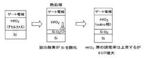
higher-kゲート絶縁膜を形成する手法はすでに提案されている。図2にそのひとつを紹介する(特許文献1参照)。これはHfO2膜上に保護膜を堆積した上で急速熱処理を行い、高誘電率の結晶相(cubic相)を優先的に生成するというものである。
しかしこの手法では、HfO2とSiとの界面に、HfO2が結晶化する際に放出された酸素によってSiO2層が形成され、ゲートスタック全体での等価酸化膜厚が増加してしまうという問題が存在し、極薄の等価酸化膜厚の実現は困難である。
higher-kゲート絶縁膜を形成する手法はすでに提案されている。図2にそのひとつを紹介する(特許文献1参照)。これはHfO2膜上に保護膜を堆積した上で急速熱処理を行い、高誘電率の結晶相(cubic相)を優先的に生成するというものである。
しかしこの手法では、HfO2とSiとの界面に、HfO2が結晶化する際に放出された酸素によってSiO2層が形成され、ゲートスタック全体での等価酸化膜厚が増加してしまうという問題が存在し、極薄の等価酸化膜厚の実現は困難である。
K.Choi et al., Tech.Dig VLSI Symp.,2009,pg.138.
T.Ando et al., IEDM 09-423~426
本発明は、HfO2層をゲート絶縁膜とするゲートスタックにおいて、界面にSiO2層が形成されない極薄の等価酸化膜厚を持ったhigher-kゲートスタックを実現することを課題とする。
上記の課題は、以下のゲートスタック形成方法によって解決される。
(1)シリコン基板上にHfO2層及び酸素吸収効果のある酸素制御金属層を順に形成する工程と、HfO2層が結晶化する温度で熱処理する工程とを含むゲートスタック形成方法。
(2)シリコン基板上にHfO2層を形成し、HfO2層とゲート電極層の間に酸素吸収効果のある酸素制御金属層を挿入した上で熱処理を行い、HfO2層を結晶化して誘電率を増大させると同時に、HfO2熱処理時の放出酸素吸収及びHfO2格子からの酸素除去効果を用いてHfO2/Si界面に形成されるSiO2を除去することを特徴とするゲートスタック形成方法。
(3)上記酸素吸収効果のある酸素制御金属層は、Ti層であることを特徴とする(1)又は(2)に記載のゲートスタック形成方法。
(4)上記ゲート電極層は、TiN電極層であることを特徴とする(2)又は(3)に記載のゲートスタック形成方法。
(1)シリコン基板上にHfO2層及び酸素吸収効果のある酸素制御金属層を順に形成する工程と、HfO2層が結晶化する温度で熱処理する工程とを含むゲートスタック形成方法。
(2)シリコン基板上にHfO2層を形成し、HfO2層とゲート電極層の間に酸素吸収効果のある酸素制御金属層を挿入した上で熱処理を行い、HfO2層を結晶化して誘電率を増大させると同時に、HfO2熱処理時の放出酸素吸収及びHfO2格子からの酸素除去効果を用いてHfO2/Si界面に形成されるSiO2を除去することを特徴とするゲートスタック形成方法。
(3)上記酸素吸収効果のある酸素制御金属層は、Ti層であることを特徴とする(1)又は(2)に記載のゲートスタック形成方法。
(4)上記ゲート電極層は、TiN電極層であることを特徴とする(2)又は(3)に記載のゲートスタック形成方法。
本発明によれば、HfO2層上に酸素吸収効果のある酸素制御金属層を形成した上で急速加熱処理を行うことにより、界面のSiO2層は形成されず、極薄の等価酸化膜厚を持ったhigher-kゲートスタックが実現できる。
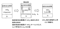
本発明に係るゲートスタック形成方法について、図1を参照して詳細に説明する。
(1)Si基板上にゲート絶縁膜となるアモルファスHfO2層及び酸素吸収効果のある酸素制御金属層を形成する。(図1左図参照)
(2)急速加熱処理を行う。(図1中央図参照)
(3)この処理によりHfO2層は結晶化し高誘電率化する。(図1右図参照)
(4)最後にゲート電極を形成しゲートスタックが完成する。
(1)Si基板上にゲート絶縁膜となるアモルファスHfO2層及び酸素吸収効果のある酸素制御金属層を形成する。(図1左図参照)
(2)急速加熱処理を行う。(図1中央図参照)
(3)この処理によりHfO2層は結晶化し高誘電率化する。(図1右図参照)
(4)最後にゲート電極を形成しゲートスタックが完成する。
酸素吸収効果のある酸素制御金属層の効果は、次のとおりである。(図1中央図参照)
(1)HfO2熱処理時の放出酸素を直接吸収し、界面のSiO2形成を抑制する。
(2)HfO2格子から酸素を除去し酸素欠陥(Vo)を膜中に導入することで、界面のSiO2を還元分解する。
これらの効果によりSiO2界面層の形成を抑制する。
(1)HfO2熱処理時の放出酸素を直接吸収し、界面のSiO2形成を抑制する。
(2)HfO2格子から酸素を除去し酸素欠陥(Vo)を膜中に導入することで、界面のSiO2を還元分解する。
これらの効果によりSiO2界面層の形成を抑制する。
本発明によれば、極薄の等価酸化膜厚を持ったhigher-kゲートスタックを実現できる。
試作では、酸素吸収効果のある金属層として5~7nmの厚さのTi層とし、熱処理温度は600~1100℃とした。これによりHfO2層の誘電率約46、HfO2ゲートスタックとして、0.37nmの等価酸化膜厚が得られた。
試作では、酸素吸収効果のある金属層として5~7nmの厚さのTi層とし、熱処理温度は600~1100℃とした。これによりHfO2層の誘電率約46、HfO2ゲートスタックとして、0.37nmの等価酸化膜厚が得られた。
Claims (4)
- シリコン基板上にHfO2層及び酸素吸収効果のある酸素制御金属層を順に形成する工程と、HfO2層が結晶化する温度で熱処理する工程とを含むゲートスタック形成方法。
- シリコン基板上にHfO2層を形成し、HfO2層とゲート電極層の間に酸素吸収効果のある酸素制御金属層を挿入した上で熱処理を行い、HfO2層を結晶化して誘電率を増大させると同時に、HfO2熱処理時の放出酸素吸収及びHfO2格子からの酸素除去効果を用いてHfO2/Si界面に形成されるSiO2を除去することを特徴とするゲートスタック形成方法。
- 上記酸素吸収効果のある酸素制御金属層は、Ti層であることを特徴とする請求項1又は2に記載のゲートスタック形成方法。
- 上記ゲート電極層は、TiN電極層であることを特徴とする請求項2又は3に記載のゲートスタック形成方法。
Applications Claiming Priority (2)
| Application Number | Priority Date | Filing Date | Title |
|---|---|---|---|
| JP2010-168792 | 2010-07-28 | ||
| JP2010168792A JP5565804B2 (ja) | 2010-07-28 | 2010-07-28 | ゲートスタック形成方法 |
Publications (1)
| Publication Number | Publication Date |
|---|---|
| WO2012014642A1 true WO2012014642A1 (ja) | 2012-02-02 |
Family
ID=45529860
Family Applications (1)
| Application Number | Title | Priority Date | Filing Date |
|---|---|---|---|
| PCT/JP2011/065430 Ceased WO2012014642A1 (ja) | 2010-07-28 | 2011-07-06 | ゲートスタック形成方法 |
Country Status (2)
| Country | Link |
|---|---|
| JP (1) | JP5565804B2 (ja) |
| WO (1) | WO2012014642A1 (ja) |
Cited By (1)
| Publication number | Priority date | Publication date | Assignee | Title |
|---|---|---|---|---|
| JP2014003050A (ja) * | 2012-06-15 | 2014-01-09 | Dainippon Screen Mfg Co Ltd | 熱処理方法および熱処理装置 |
Families Citing this family (3)
| Publication number | Priority date | Publication date | Assignee | Title |
|---|---|---|---|---|
| JP5652926B2 (ja) * | 2011-03-28 | 2015-01-14 | 独立行政法人産業技術総合研究所 | ゲート絶縁膜の形成方法及び半導体装置の製造方法 |
| JP5692801B2 (ja) * | 2011-03-30 | 2015-04-01 | 独立行政法人産業技術総合研究所 | 半導体の製造方法及び半導体装置 |
| KR20140032716A (ko) | 2012-09-07 | 2014-03-17 | 삼성전자주식회사 | 반도체 장치 및 그 제조 방법 |
Citations (3)
| Publication number | Priority date | Publication date | Assignee | Title |
|---|---|---|---|---|
| JP2000260979A (ja) * | 1999-03-11 | 2000-09-22 | Toshiba Corp | 半導体装置およびその製造方法 |
| JP2008537359A (ja) * | 2005-04-21 | 2008-09-11 | インターナショナル・ビジネス・マシーンズ・コーポレーション | 自己整合され積極的にスケーリングされたcmosデバイスにおけるゲート電極の金属/金属窒化物二重層のcmos構造体及び半導体構造体 |
| JP2008306036A (ja) * | 2007-06-08 | 2008-12-18 | Seiko Epson Corp | 半導体装置の製造方法及び半導体装置 |
-
2010
- 2010-07-28 JP JP2010168792A patent/JP5565804B2/ja not_active Expired - Fee Related
-
2011
- 2011-07-06 WO PCT/JP2011/065430 patent/WO2012014642A1/ja not_active Ceased
Patent Citations (3)
| Publication number | Priority date | Publication date | Assignee | Title |
|---|---|---|---|---|
| JP2000260979A (ja) * | 1999-03-11 | 2000-09-22 | Toshiba Corp | 半導体装置およびその製造方法 |
| JP2008537359A (ja) * | 2005-04-21 | 2008-09-11 | インターナショナル・ビジネス・マシーンズ・コーポレーション | 自己整合され積極的にスケーリングされたcmosデバイスにおけるゲート電極の金属/金属窒化物二重層のcmos構造体及び半導体構造体 |
| JP2008306036A (ja) * | 2007-06-08 | 2008-12-18 | Seiko Epson Corp | 半導体装置の製造方法及び半導体装置 |
Non-Patent Citations (3)
| Title |
|---|
| CHANGHWAN CHOI ET AL.: "Fabrication of TaN-gated Ultra-Thin MOSFETs(EOT<1.0nm) with Hf02 using a Novel Oxygen Scavenging Process for sub 65nm Application", 2005 SYMPOSIOUM ON VLSI TECHNOLOGY DIGEST OF TECHNICAL PAPERS, 2005, pages 226 - 227, XP010818308, DOI: doi:10.1109/.2005.1469277 * |
| HYOUNGSUB KIM ET AL.: "Engineering chemically abrupt high-k metal oxide/silicon interfaces using an oxygen-gettering metal overlayer", JOURNAL OF APPLIED PHYSICS, vol. 96, no. 6, 15 September 2004 (2004-09-15), pages 3467 - 3472, XP012068842, DOI: doi:10.1063/1.1776636 * |
| SUNGHO HEO ET AL.: "Laser Annealing on Ti Electrode:Impact on Ti/Hf02/Si02 n-Type MOSFET", ELECTROCHEMICAL AND SOLID-STATE LETTERS, vol. 11, no. 10, 2008, pages H276 - H279 * |
Cited By (1)
| Publication number | Priority date | Publication date | Assignee | Title |
|---|---|---|---|---|
| JP2014003050A (ja) * | 2012-06-15 | 2014-01-09 | Dainippon Screen Mfg Co Ltd | 熱処理方法および熱処理装置 |
Also Published As
| Publication number | Publication date |
|---|---|
| JP2012028713A (ja) | 2012-02-09 |
| JP5565804B2 (ja) | 2014-08-06 |
Similar Documents
| Publication | Publication Date | Title |
|---|---|---|
| JP6192577B2 (ja) | グラフェン系の電界効果トランジスタ | |
| CN103681276B (zh) | 金属栅极、mos晶体管及cmos结构分别的形成方法 | |
| CN102104070B (zh) | 半导体结构及其形成方法 | |
| CN105226022B (zh) | 半导体结构的形成方法 | |
| JP2010505274A5 (ja) | ||
| CN103594365A (zh) | Pmos晶体管的形成方法 | |
| US9508859B2 (en) | TFT array substrate and manufacturing method of the same | |
| JP2008283182A (ja) | Pmosトランジスタ製造方法及びcmosトランジスタ製造方法 | |
| JP5565804B2 (ja) | ゲートスタック形成方法 | |
| JP2008532282A (ja) | 窒化ゲート誘電体を形成する方法 | |
| JP2009055030A (ja) | 結晶質アルミニウム酸化物層のエネルギーバンドギャップを高める方法及びエネルギーバンドギャップの高い結晶質アルミニウム酸化物層を備える電荷トラップメモリ素子の製造方法 | |
| CN1195317C (zh) | 超薄氮化硅/氧化硅栅极介电层的制造方法 | |
| CN103367135A (zh) | 栅极堆叠形成期间于高介电栅极介电层中钝化点缺陷 | |
| JP2004186567A (ja) | 半導体装置および半導体装置の製造方法 | |
| JP5652926B2 (ja) | ゲート絶縁膜の形成方法及び半導体装置の製造方法 | |
| CN103646865A (zh) | 在Ge衬底制备超薄氧化锗界面修复层的方法 | |
| TWI593023B (zh) | 晶圓的形成方法 | |
| Lehmann et al. | Millisecond flash lamp annealing for LaLuO3 and LaScO3 high-k dielectrics | |
| JP4590556B2 (ja) | 半導体装置の製造方法 | |
| WO2012014775A1 (ja) | 半導体装置及びその製造方法 | |
| CN103184438B (zh) | 薄膜的热处理方法及热处理装置、化学气相沉积装置 | |
| JP2008306132A (ja) | 半導体装置の製造方法 | |
| CN103165440A (zh) | 高介电常数金属栅极半导体器件制造方法 | |
| CN102810468B (zh) | 一种高k栅介质界面优化方法 | |
| CN114496920B (zh) | 高介电常数金属栅的制造方法 |
Legal Events
| Date | Code | Title | Description |
|---|---|---|---|
| 121 | Ep: the epo has been informed by wipo that ep was designated in this application |
Ref document number: 11812234 Country of ref document: EP Kind code of ref document: A1 |
|
| NENP | Non-entry into the national phase |
Ref country code: DE |
|
| 122 | Ep: pct application non-entry in european phase |
Ref document number: 11812234 Country of ref document: EP Kind code of ref document: A1 |