WO2012008252A1 - 化学機械研磨パッドおよび化学機械研磨方法 - Google Patents
化学機械研磨パッドおよび化学機械研磨方法 Download PDFInfo
- Publication number
- WO2012008252A1 WO2012008252A1 PCT/JP2011/063500 JP2011063500W WO2012008252A1 WO 2012008252 A1 WO2012008252 A1 WO 2012008252A1 JP 2011063500 W JP2011063500 W JP 2011063500W WO 2012008252 A1 WO2012008252 A1 WO 2012008252A1
- Authority
- WO
- WIPO (PCT)
- Prior art keywords
- chemical mechanical
- mechanical polishing
- polishing
- polishing pad
- layer
- Prior art date
- Legal status (The legal status is an assumption and is not a legal conclusion. Google has not performed a legal analysis and makes no representation as to the accuracy of the status listed.)
- Ceased
Links
Images


Classifications
-
- B—PERFORMING OPERATIONS; TRANSPORTING
- B24—GRINDING; POLISHING
- B24B—MACHINES, DEVICES, OR PROCESSES FOR GRINDING OR POLISHING; DRESSING OR CONDITIONING OF ABRADING SURFACES; FEEDING OF GRINDING, POLISHING, OR LAPPING AGENTS
- B24B37/00—Lapping machines or devices; Accessories
- B24B37/11—Lapping tools
- B24B37/20—Lapping pads for working plane surfaces
- B24B37/26—Lapping pads for working plane surfaces characterised by the shape of the lapping pad surface, e.g. grooved
-
- B—PERFORMING OPERATIONS; TRANSPORTING
- B24—GRINDING; POLISHING
- B24B—MACHINES, DEVICES, OR PROCESSES FOR GRINDING OR POLISHING; DRESSING OR CONDITIONING OF ABRADING SURFACES; FEEDING OF GRINDING, POLISHING, OR LAPPING AGENTS
- B24B37/00—Lapping machines or devices; Accessories
- B24B37/11—Lapping tools
- B24B37/20—Lapping pads for working plane surfaces
- B24B37/24—Lapping pads for working plane surfaces characterised by the composition or properties of the pad materials
-
- H—ELECTRICITY
- H10—SEMICONDUCTOR DEVICES; ELECTRIC SOLID-STATE DEVICES NOT OTHERWISE PROVIDED FOR
- H10P—GENERIC PROCESSES OR APPARATUS FOR THE MANUFACTURE OR TREATMENT OF DEVICES COVERED BY CLASS H10
- H10P52/00—Grinding, lapping or polishing of wafers, substrates or parts of devices
-
- H—ELECTRICITY
- H10—SEMICONDUCTOR DEVICES; ELECTRIC SOLID-STATE DEVICES NOT OTHERWISE PROVIDED FOR
- H10P—GENERIC PROCESSES OR APPARATUS FOR THE MANUFACTURE OR TREATMENT OF DEVICES COVERED BY CLASS H10
- H10P52/00—Grinding, lapping or polishing of wafers, substrates or parts of devices
- H10P52/40—Chemomechanical polishing [CMP]
- H10P52/402—Chemomechanical polishing [CMP] of semiconductor materials
-
- H—ELECTRICITY
- H10—SEMICONDUCTOR DEVICES; ELECTRIC SOLID-STATE DEVICES NOT OTHERWISE PROVIDED FOR
- H10P—GENERIC PROCESSES OR APPARATUS FOR THE MANUFACTURE OR TREATMENT OF DEVICES COVERED BY CLASS H10
- H10P52/00—Grinding, lapping or polishing of wafers, substrates or parts of devices
- H10P52/40—Chemomechanical polishing [CMP]
- H10P52/403—Chemomechanical polishing [CMP] of conductive or resistive materials
-
- H—ELECTRICITY
- H10—SEMICONDUCTOR DEVICES; ELECTRIC SOLID-STATE DEVICES NOT OTHERWISE PROVIDED FOR
- H10P—GENERIC PROCESSES OR APPARATUS FOR THE MANUFACTURE OR TREATMENT OF DEVICES COVERED BY CLASS H10
- H10P95/00—Generic processes or apparatus for manufacture or treatments not covered by the other groups of this subclass
- H10P95/06—Planarisation of inorganic insulating materials
- H10P95/062—Planarisation of inorganic insulating materials involving a dielectric removal step
Definitions
- the present invention relates to a chemical mechanical polishing pad and a chemical mechanical polishing method using the chemical mechanical polishing pad.
- CMP chemical mechanical polishing
- the wafer surface (surface to be polished) on which elements and wiring are fabricated is slid against the surface of the chemical mechanical polishing pad while being slid against each other while being pressed against the polishing layer of the chemical mechanical polishing pad.
- This is a mechanical polishing technique.
- the polishing rate, the scratch on the surface to be polished, the in-plane uniformity of the surface to be polished, etc. vary greatly depending on the properties and characteristics of the chemical mechanical polishing pad.
- JP-A-11-70463 discloses a chemical mechanical polishing pad made of a foamed resin such as polyurethane foam
- JP-A 2000-34416 discloses a non-foamed matrix
- a chemical mechanical polishing pad having water-soluble particles dispersed therein is disclosed.
- Japanese Patent No. 3769581 provides a recess for expressing good polishing characteristics in the polishing layer of the chemical mechanical polishing pad and improves the smoothness of the inner surface such as the side surface or the bottom surface of the recess.
- a technique for increasing the fluidity of a slurry is disclosed.
- the chemical mechanical polishing pad having a recess on the surface of the polishing layer as described above is exposed to the slurry for a long time in the chemical mechanical polishing process, it is included in the slurry from the inner surface of the recess. Intrusion of components such as moisture may cause deformation of the recess.
- the polishing characteristics may be deteriorated such as a scratch on the surface to be polished during chemical mechanical polishing, a slurry distribution function, and a waste discharge function.
- some aspects of the present invention provide a chemical mechanical polishing pad that can maintain good polishing characteristics even when exposed to a slurry for a long time by solving the above-described problems, and the chemical mechanical A chemical mechanical polishing method using a polishing pad is provided.
- the present invention has been made to solve at least a part of the above-described problems, and can be realized as the following aspects or application examples.
- a chemical mechanical polishing pad with a polishing layer The surface provided for polishing of the polishing layer is provided with a recess, The polishing layer has a surface layer portion including at least the inner surface of the recess, The polishing layer is immersed in water at 23 ° C. for 1 hour with respect to the average opening ratio D2 (%) in the cross section when the section obtained by cutting the polishing layer at a surface not intersecting with the surface layer portion is immersed in water at 23 ° C. for 1 hour.
- the ratio (D1 / D2) of the average aperture ratio D1 (%) on the inner surface of the recess when immersed is 0.01 or more and 0.5 or less.
- the average aperture ratio D1 (%) may be 0.1% or more and 20% or less.
- the average aperture ratio D2 (%) may be 10% or more and 50% or less.
- the surface roughness (Ra) on the inner surface of the recess may be 1 ⁇ m or more and 10 ⁇ m or less.
- the silicon atom concentration or fluorine atom concentration calculated by elemental analysis of the surface to be polished of the polishing layer by X-ray photoelectron spectroscopy (XPS) is 0.5 atom% or more and 10 atom% or less. it can.
- the silicon atom concentration or the fluorine atom concentration calculated by elemental analysis of the inner surface of the concave portion by X-ray photoelectron spectroscopy (XPS) may be 0.5 atom% or more and 10 atom% or less.
- One aspect of the chemical mechanical polishing method according to the present invention is: Chemical mechanical polishing is performed using the chemical mechanical polishing pad of any one of Application Examples 1 to 6.
- the chemical mechanical polishing pad according to the present invention can reduce the entry of the slurry component from the inner surface of the recess provided in the polishing layer even when it is exposed to the slurry for a long time in the chemical mechanical polishing step. Therefore, good polishing characteristics can be maintained. Further, since the chemical mechanical polishing method according to the present invention uses the above-described chemical mechanical polishing pad, it always exhibits a certain polishing performance even when it is exposed to the slurry for a long time in the chemical mechanical polishing step. be able to.
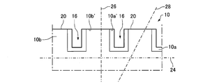
- FIG. 1 is a cross-sectional view schematically showing a chemical mechanical polishing pad according to the present embodiment.
- FIG. 2 is an enlarged view of region I in FIG.
- FIG. 3 is an enlarged view of region I in FIG. 1 after use of the chemical mechanical polishing pad.
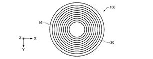
- FIG. 4 is a plan view schematically showing the chemical mechanical polishing pad according to the present embodiment.
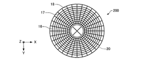
- FIG. 5 is a plan view schematically showing the chemical mechanical polishing pad according to the first modification.
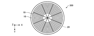
- FIG. 6 is a plan view schematically showing a chemical mechanical polishing pad according to a second modification.
- the structure of the chemical mechanical polishing pad according to the present embodiment is not particularly limited as long as it has a polishing layer on at least one surface.
- the surface (hereinafter also referred to as “polishing surface”) used for polishing the polishing layer is provided with a recess. Further, the polishing layer has a surface layer portion including at least the inner surface of the recess.
- FIG. 1 is a cross-sectional view schematically showing an example of a chemical mechanical polishing pad according to the present embodiment.
- the chemical mechanical polishing pad 100 includes a polishing layer 10 and a support layer 12 formed on the surface side of the polishing layer 10 that comes into contact with the polishing apparatus surface plate 14.
- polishing layer Although the planar shape of the polishing layer 10 is not specifically limited, For example, it can be circular. When the planar shape of the polishing layer 10 is circular, the size is preferably 150 mm to 1200 mm in diameter, more preferably 500 mm to 1000 mm in diameter. The thickness of the polishing layer 10 is preferably 0.5 mm to 5.0 mm, more preferably 1.0 mm to 4.0 mm, and particularly preferably 1.5 mm to 3.5 mm.
- FIG. 2 is an enlarged view of the region I in FIG. 1, and is a cross-sectional view schematically showing the detailed shape of the polishing layer 10.
- the polishing surface 20 is provided with a plurality of recesses 16.
- the recess 16 holds the slurry supplied during chemical mechanical polishing, distributes it uniformly to the polishing surface 20, and temporarily retains waste such as polishing debris and used slurry to the outside. It has a function as a route for discharging.
- the cross-sectional shape of the recess 16 is not particularly limited, but may be, for example, a shape formed from flat side surfaces and a bottom surface, a polygonal shape, a U shape, a V shape, or the like.
- the depth a of the recess 16 is preferably 0.1 mm or more, more preferably 0.1 mm to 2.5 mm, and particularly preferably 0.2 mm to 2.0 mm.
- the width b of the recess 16 can be 0.1 mm or more, more preferably 0.1 mm to 5.0 mm, and particularly preferably 0.2 mm to 3.0 mm.
- the interval c between the adjacent recesses 16 is preferably 0.05 mm or more, more preferably 0.05 mm to 100 mm, and particularly preferably 0.1 mm to 10 mm.
- the pitch d which is the sum of the width of the recess and the distance between the adjacent recesses, is preferably 0.15 mm or more, more preferably 0.15 mm to 105 mm, and particularly preferably 0.6 mm to 13 mm. it can.
- the depth a is 0.1 mm or more
- the width b is 0.1 mm or more
- the interval c is 0.05 mm or more
- the depth a is 0.1 mm to 2.5 mm
- the width b is 0.
- the distance c is 0.05 mm to 100 mm
- the depth a is 0.2 mm to 2.0 mm
- the width b is 0.2 mm to 3.0 mm
- the distance c is 0.00 mm.
- a thickness of 1 mm to 10 mm is particularly preferable.
- the polishing layer 10 is composed of a surface layer portion 10a and a deep layer portion 10b.
- the surface layer portion 10 a is formed to include the polishing surface 20 and the inner surface of the recess 16.
- the surface layer portion 10 a including the polishing surface 20 is gradually worn, and only the surface layer portion 10 a including the inner surface of the recess 16 remains. Therefore, in the polishing layer 10, the surface layer portion 10 a including at least the inner surface of the recess 16 remains regardless of the use stage of the chemical mechanical polishing pad 100.
- the “inner surface of the recess” means an inner surface of the recess such as a side surface and a bottom surface.
- the surface layer portion 10a is not particularly limited, but is preferably a region of 100 ⁇ m or less from the inner surface of the polishing surface 20 or the recess 16, and more preferably a region of 10 ⁇ m or less.
- the deep layer portion 10b refers to a region of the polishing layer 10 other than the surface layer portion 10a.
- the chemical mechanical polishing pad 100 has the following characteristics.
- D1 be the average aperture ratio (%) on the inner surface of the recess 16 when the polishing layer 10 is immersed in water at 23 ° C. for 1 hour.
- a cross section obtained by cutting the polishing layer 10 at a surface that does not intersect the surface layer portion 10a is prepared, and the average opening ratio (%) in the cross section when the cross section is immersed in water at 23 ° C. for 1 hour is defined as D2.
- the ratio (D1 / D2) of D1 to D2 of the chemical mechanical polishing pad 100 according to the present embodiment is 0.01 or more and 0.5 or less.
- the ratio (D1 / D2) is more preferably 0.1 or more and 0.4 or less.
- the chemical mechanical polishing pad 100 has the following features and effects as described above.
- the polishing surface 20 of the polishing layer 10 can be a surface having a larger average aperture ratio by exposing the deep layer portion 10b by removing the surface layer portion 10a due to dressing or wear. As a result, the slurry holding function of the polishing surface 20 is improved, and the polishing rate can be improved.
- the inner surface of the recess 16 in the polishing layer 10 does not lose the surface layer portion 10a having a smaller average aperture ratio due to dressing or wear, so that the entry of slurry components from the inner surface of the recess 16 into the polishing layer 10 is reduced. Can do.
- FIG. 3 is an enlarged view of the region I in FIG. 1, and is a cross-sectional view schematically showing the detailed shape of the polishing layer 10 after the chemical mechanical polishing pad 100 is used.
- the surface layer portion 10a disappears due to dressing or wear and the deep layer portion 10b ′ is exposed.
- the surface layer portion 10a ′ is also exposed.
- CMP CMP is performed on the polishing surface 20 in such a state, since the average opening ratio is different between the surface layer portion 10a ′ and the deep layer portion 10b ′, a difference in slurry holding performance occurs depending on the portion of the polishing surface 20 and polishing such as scratching is performed. Scratches may occur.
- the ratio (D1 / D2) is within the above range, the difference in slurry holding performance based on the portion of the polishing surface 20 can be reduced, so that polishing scratches such as scratches can be generated. Can be reduced.
- the ratio (D1 / D2) is less than 0.01, the difference in the average opening ratio between the surface layer portion 10a ′ and the deep layer portion 10b ′ is too large. Abrasion scratches such as scratches may occur.
- the average aperture ratio D1 (%) is preferably 0.1% or more and 20% or less, and more preferably 1% or more and 15% or less.
- the average opening ratio D1 is within the above range, the effect of reducing the entry of the slurry component from the inner surface of the recess 16 into the polishing layer 10 is easily obtained. Accordingly, even during chemical mechanical polishing using a slurry that is an aqueous dispersion of abrasive grains, the entry of slurry components from the inner surface of the recess 16 into the polishing layer 10 is reduced, so that deformation of the recess 16 can be prevented. it can.
- the average aperture ratio D2 (%) is preferably 10% or more and 50% or less, and more preferably 20% or more and 40% or less.
- the polishing layer 20 is made a surface having a larger average aperture ratio by causing the surface layer portion 10a to disappear and exposing the deep layer portion 10b by dressing or wear. Can do.
- the slurry holding function of the polishing surface 20 is improved, and the polishing rate can be improved.
- the average aperture ratio D2 (%) is in the above range, the structure of the deep layer portion 10b is strong, and the shape of the recess 16 is maintained as it is even when the recess 16 is formed. Thereby, the flatness of the surface to be polished may be improved.
- the average aperture ratio D2 (%) can be measured as follows. First, a cross section is produced by cutting the polishing layer 10 on a surface that does not intersect the surface layer portion 10a of the polishing layer 10. As a specific example of the cross section thus produced, in the case shown in FIG. 2 (that is, when the surface layer portion 10a including the polishing surface 20 remains), for example, with respect to the polishing surface 20 The cross section 22 cut
- the cross section thus produced is a cross section of the deep layer portion 10b. Subsequently, 23 degreeC water is put into a container and the obtained cross section is immersed in the water for 1 hour. Thereafter, the average aperture ratio D2 (%) can be obtained by using the same method as the above-described average aperture ratio D1 (%).
- the silicon atom concentration or the fluorine atom concentration calculated by measuring at a photoelectron extraction angle of 90 ° with respect to the surface to be provided is 0.5 atom% or more and 10 atom% or less. That is, in the chemical mechanical polishing pad 100 shown in FIG. 1, it can be said that the silicon atom concentration or the fluorine atom concentration in the surface layer portion 10a is preferably 0.5 atom% or more and 10 atom% or less.
- the silicon atom concentration in the surface layer portion 10a is preferably 1 atom% or more and 9 atom% or less, and more preferably 1.5 atom% or more and 7 atom% or less.
- the fluorine atom concentration in the surface layer portion 10a is preferably 1 atom% or more and 9 atom% or less, and more preferably 1.5 atom% or more and 7 atom% or less.
- the silicon atom concentration or the fluorine atom concentration in the surface layer portion 10a is in the above range, the balance between hydrophobicity and hydrophilicity in the surface layer portion 10a is improved, so that the slurry holding function in the polishing step is not impaired, and the surface layer portion 10a It is possible to prevent the slurry from penetrating into the deep layer portion 10b.
- the total of the silicon atom concentration and the fluorine atom concentration in the surface layer portion 10a is preferably 0.5 atom% or more and 10 atom% or less, and preferably 1 atom% or more and 9 atom% or less, from the viewpoint of easily obtaining the above-described effect. More preferred.
- the chemical mechanical polishing pad 100 includes the surface layer portion 10a in which the silicon atom concentration or the fluorine atom concentration on the inner surface of the recess 16 is 0.5 atom% or more and 10 atom% or less, the polishing surface 20 is in the polishing process. Even if worn, the surface layer portion 10a existing on the inner surface does not disappear due to wear. Therefore, the surface layer portion 10a existing in the recess 16 can prevent the slurry from penetrating from the inner surface of the recess 16 to the deep layer portion 10b in the polishing process.
- the silicon atom concentration and the fluorine atom concentration in the deep layer portion 10b of the polishing layer 10 are preferably 0 atom% or more and 0.1 atom% or less from the viewpoint of suppressing contamination of the object to be polished in the polishing process.
- the deep layer part 10b does not contain a silicon and a fluorine from the viewpoint mentioned above.
- the silicon atom concentration and the fluorine atom concentration in the deep layer portion 10b can be determined, for example, as follows. First, argon ion etching is performed on the surface of the polishing layer 10 to be polished, and the surface layer portion 10a of the polishing layer 10 is completely removed to expose the deep layer portion 10b. Next, the surface of the deep layer portion 10b is irradiated with X-rays using XPS, and the generated photoelectrons are measured at a photoelectron extraction angle of 90 ° with respect to the deep layer portion 10b, whereby the silicon atom concentration and fluorine in the deep layer portion 10b are measured. Atomic concentration can be calculated.
- the silicon atom concentration and the fluorine atom concentration are silicon or fluorine atoms when the total of all atom number quantification values having an atomic number equal to or greater than the atomic number of the carbon atom measured by XPS is 100 atom%. It represents the ratio of the number of atoms.
- the silicon atom concentration and the fluorine atom concentration present in the polishing layer 10 are measured by using XPS, and the principle of XPS is generally as follows.
- XPS is a spectroscopic method that measures the energy of photoelectrons emitted from a sample by X-ray irradiation. Since photoelectrons collide with molecules and are scattered immediately in the atmosphere, it is necessary to keep the apparatus in a vacuum. Also, photoelectrons emitted deep inside the solid sample are scattered within the sample and cannot escape from the surface. Therefore, XPS is effective as a surface analysis method because it measures photoelectrons only from the sample surface.
- the method for measuring the electron energy is not particularly limited, but a representative one is an electrostatic field type in which electrons are introduced into an electrostatic field and only a fixed orbit is detected.
- binding energy E K electrons By XPS, it is possible to measure the binding energy E K electrons. Since such binding energy is basically a value inherent to the element, the type of element can be specified. Each element can also be quantified from the intensity of the photoelectron spectrum.
- the photoelectrons are isotropically emitted from the surface of the sample, but the escape depth of the photoelectrons from the solid surface varies depending on the photoelectron extraction angle.
- the escape depth is maximized by setting the photoelectron extraction angle to 90 ° with respect to the sample surface, and information on a deeper portion on the surface of the sample can be obtained.
- the “photoelectron take-off angle” means an angle formed between the sample surface and the detector.
- the apparatus used for XPS is not particularly limited as long as it can analyze the qualitative, quantitative, and chemical state of the elements present on the surface of the sample.
- model “Quantum 2000” manufactured by ULVAC-PHI Co., Ltd. may be used.
- the surface roughness (Ra) of the inner surface of the recess 16 is preferably 1 ⁇ m or more and 10 ⁇ m or less. If the surface roughness (Ra) of the inner surface of the recess 16 is in the above range, it can be said that there is substantially no unevenness on the inner surface of the recess 16 that causes scratches during chemical mechanical polishing. In the case where there are irregularities, particularly large convex portions (for example, uncut parts generated when the concave portions 16 are formed) on the inner surface of the concave portions 16, the convex portions are detached during the CMP, thereby scratching the surface to be polished. May cause.
- the function as the recess in addition to preventing scratches, the function as the recess, in particular, the function of distributing the slurry to the polishing surface and the waste are discharged to the outside. The function to perform is demonstrated efficiently.
- the surface roughness (Ra) of the inner surface of the recess can be measured as follows. First, using a surface roughness measuring machine (for example, “SURFTEST” manufactured by Mitutoyo Corporation) for an arbitrary portion of the inner surface of the concave portion provided in the polishing layer of the chemical mechanical polishing pad before use, a speed of 0. A roughness curve of 5 sections is measured twice in the longitudinal and lateral directions under the conditions of 5 mm / s and a reference length of 0.8 mm. From the obtained roughness curve, the average of the absolute values of deviations from the average line to the measurement curve is defined as the surface roughness (Ra) of the inner surface of the recess.
- a surface roughness measuring machine for example, “SURFTEST” manufactured by Mitutoyo Corporation
- FIG. 4 is a plan view of the chemical mechanical polishing pad 100 according to the present embodiment.
- the recess 16 can be formed in a plurality of concentric circles whose diameter gradually increases from the center of the polishing surface 20 toward the outer edge.
- FIG. 5 is a plan view of the chemical mechanical polishing pad 200 according to the first modification, and corresponds to FIG.
- the chemical mechanical polishing pad 200 according to the first modification further includes a plurality of recesses 17 and recesses 18 extending radially from the center of the polishing surface 20 toward the outer edge in addition to the plurality of recesses 16 provided in an annular shape. It differs from the chemical mechanical polishing pad 100 in that it includes.
- the center portion refers to a region surrounded by a circle having a radius of 50 mm with the center of gravity of the polishing layer as the center.
- the concave portion 17 and the concave portion 18 need only extend from an arbitrary position in the “center portion” in the outer edge direction, and the shape thereof may be, for example, a linear shape, an arc shape, or a combination thereof.
- the cross-sectional shapes of the recess 17 and the recess 18 can be the same as the recess 16 described above.
- Other configurations of the chemical mechanical polishing pad 200 according to the first modification are the same as the configurations of the polishing layer 10 described with reference to FIGS.
- FIG. 6 is a plan view of a chemical mechanical polishing pad 300 according to a second modification, and corresponds to FIG.
- the chemical mechanical polishing pad 300 according to the second modified example further includes a plurality of recesses 19 extending radially from the center of the polishing surface 20 toward the outer edge in addition to the plurality of recesses 16 provided in an annular shape. It differs from the chemical mechanical polishing pad 100 described above.
- the cross-sectional shape of the recess 19 can be the same as the recess 16 described above.
- the other configuration of the chemical mechanical polishing pad 300 according to the second modification is the same as the configuration of the polishing layer 10 described with reference to FIGS.
- planar shape of the concave portion has been described above, the planar shape of the concave portion is not particularly limited to the above-described embodiment, and can be appropriately optimized depending on the object to be polished.
- the planar shape of the recess may be, for example, a polygonal shape such as a triangle, a quadrangle, or a pentagon, an ellipse, or a spiral. Further, the number of recesses provided on the polishing surface is not particularly limited.
- the polishing layer 10 may be made of any material as long as the object of the present invention can be achieved.
- the recess 16 has a function of holding slurry during chemical mechanical polishing and temporarily retaining polishing waste.
- the polishing layer 10 is preferably made of a material made of a water-insoluble matrix in which water-soluble particles are dispersed or a material made of a water-insoluble matrix in which pores are dispersed, such as a foam.
- the support layer 12 is used in the chemical mechanical polishing pad 100 to support the polishing layer 10 on the polishing apparatus surface plate 14.
- the support layer 12 may be an adhesive layer or a cushion layer having the adhesive layer on both sides.
- the adhesive layer can be made of, for example, an adhesive sheet.
- the thickness of the pressure-sensitive adhesive sheet is preferably 50 ⁇ m to 250 ⁇ m. By having a thickness of 50 ⁇ m or more, the pressure from the polishing surface 20 side of the polishing layer 10 can be sufficiently relaxed, and by having a thickness of 250 ⁇ m or less, the influence of unevenness on the polishing performance is not affected. A chemical mechanical polishing pad 100 having a uniform thickness is obtained.
- the material of the pressure-sensitive adhesive sheet is not particularly limited as long as the polishing layer 10 can be fixed to the polishing apparatus surface plate 14, but is preferably an acrylic or rubber-based material having a lower elastic modulus than the polishing layer 10.
- the adhesive strength of the pressure-sensitive adhesive sheet is not particularly limited as long as the chemical mechanical polishing pad 100 can be fixed to the surface plate 14 for polishing apparatus, but when the adhesive strength of the pressure-sensitive adhesive sheet is measured according to the standard of “JIS Z0237”, the adhesive strength thereof Is preferably 3 N / 25 mm or more, more preferably 4 N / 25 mm or more, and particularly preferably 10 N / 25 mm or more.
- the cushion layer is made of a material whose hardness is lower than that of the polishing layer 10, the material is not particularly limited, and may be a porous body (foam) or a non-porous body.
- a cushion layer the layer which shape
- the thickness of the cushion layer is preferably 0.1 mm to 5.0 mm, more preferably 0.5 mm to 2.0 mm.
- the chemical mechanical polishing pad according to the present embodiment can be produced, for example, by a molding method using a mold or by coating the surface of the polishing layer with a non-foaming material.
- a molding method using a mold or by coating the surface of the polishing layer with a non-foaming material.
- an example of a method for manufacturing a chemical mechanical polishing pad will be described.
- a foamed resin block such as polyurethane foam is prepared and then sliced.
- a non-foamable material is further applied to the surface.
- the surface layer portion is formed by applying the material to the inner surface of the recess, and the above-described chemical mechanical polishing pad can be manufactured.
- the chemical mechanical polishing pad according to the present embodiment can be manufactured by a method including a step of preparing a composition containing at least polyurethane and a step of molding the composition using a mold. it can.
- the surface of the mold is preferably coated with a material containing at least one element selected from silicon and fluorine from the viewpoint of efficiently producing the chemical mechanical polishing pad described above.
- a method for producing a chemical mechanical polishing pad using a mold will be described.
- the material of the mold is not particularly limited, and examples thereof include aluminum, carbon steel, tool steel, and ceramic.
- the surface shape of the mold to be used may be flat, but it is preferable to have a concave pattern for molding the concave shape as described in the section “1. Chemical mechanical polishing pad”. By providing the mold with the concave pattern, the concave pattern can be efficiently transferred to the molded polishing layer.
- the shape of the concave pattern is not particularly limited, and may be, for example, a spiral shape, an annular shape, a lattice shape or the like in plan view.
- the diameter of the ring is preferably 1 mm to 1100 mm, more preferably 1 mm to 1000 mm, and particularly preferably 2 mm to 850 mm.
- the width of the concave is preferably 0.1 mm to 5.0 mm, and preferably 0.2 mm to 3.0 mm. More preferred.
- the depth of the recess is preferably 0.1 mm to 2.5 mm, more preferably 0.2 mm to 2.0 mm, and more preferably 0.2 mm to 1.5 mm regardless of the shape of the recess pattern. It is particularly preferred. These recess patterns may be formed by a single line or only one, or may be formed by two or more lines or two or more.
- the arithmetic surface roughness (Ra) of the mold surface is preferably 20 ⁇ m or less, more preferably 15 ⁇ m or less, from the viewpoint of improving the peelability of the polishing layer from the mold.
- the arithmetic surface roughness of the mold surface can be measured by using, for example, an optical surface roughness measuring device, a contact surface roughness measuring device, or the like.
- the optical surface roughness measuring device include a three-dimensional surface structure analysis microscope, a scanning laser microscope, and an electron beam surface morphology analyzer.
- Examples of the contact type surface roughness measuring device include a stylus type surface roughness meter.
- a composition containing at least polyurethane is prepared.
- a polyurethane it does not specifically limit as a polyurethane, It is preferable to use a thermoplastic polyurethane. If necessary, additives such as water-soluble particles, a crosslinking agent, a crosslinking aid, an organic filler, and an inorganic filler may be added to such a composition.
- the mold is filled with the composition, and a polishing layer is molded by means such as compression molding or extrusion molding.
- a crosslinking agent is added to the composition
- the mold is preferably preheated to a temperature of 160 ° C. to 220 ° C., more preferably 170 ° C. to 210 ° C., and then crosslinked and molded. Good.
- the plasticized composition is molded by a press machine or an injection molding machine and solidified by cooling, or plasticized using an extruder equipped with a T die. -Molding may be performed by using a sheeting method.
- the recess may be formed by means such as cutting after molding.
- the non-foamable material that can be applied is preferably a material containing at least one element selected from silicon and fluorine, specifically, silicon, silicone, silicon dioxide, silicon nitride, silicic acid, Contains at least one selected from silicon carbide, silicate, silicon resin, organosilane, siloxide, silylhydride, silene, polytetrafluoroethylene, polyvinylidene fluoride, fluororesin, metal fluoride, and nonmetal fluoride A composition.
- a surface treatment other than applying a material containing at least one element selected from silicon and fluorine can be optionally performed on the mold to be used.
- Optional surface treatments include, for example, electroplating, hot dipping, diffusion plating, vapor deposition plating, electroless plating, thermal spraying, chemical conversion treatment, flame quenching, induction quenching, carburization, nitriding, electron beam quenching, laser firing. And shot peening.
- Chemical mechanical polishing method using chemical mechanical polishing pad is characterized in that chemical mechanical polishing is performed using the chemical mechanical polishing pad described above.
- the chemical mechanical polishing pad described above can reduce the entry of slurry components from the inner surface of the recess provided in the polishing layer even when exposed to the slurry for a long time in the chemical mechanical polishing step. Good polishing characteristics can be maintained. Since the chemical mechanical polishing method according to the present embodiment uses such a chemical mechanical polishing pad, it always exhibits a constant polishing performance even when it is exposed to the slurry for a long time in the chemical mechanical polishing step. can do.
- a commercially available chemical mechanical polishing apparatus can be used.
- Examples of commercially available chemical mechanical polishing apparatuses include model “EPO-112”, model “EPO-222” (above, manufactured by Ebara Corporation); model “LGP-510”, model “LGP-552” (above, Wrap master SFT); model “Mirra” (Applied Materials) and the like.
- an optimal one can be selected as appropriate according to the object to be polished (copper film, insulating film, low dielectric constant insulating film, etc.).
- Example 4.1 Example 1 35 parts by mass of thermoplastic polyurethane (BASF, trade name “Elastolan 1174D”), 35 parts by weight of thermoplastic polyurethane (trade name “Elastolan NY97A”), ⁇ -cyclodextrin (brine) as water-soluble particles
- a thermoplastic polyurethane composition was obtained by kneading 30 parts by mass of Minato Seika Co., Ltd. (trade name “Dexy Pearl ⁇ -100”) with a rudder heated to 180 ° C.
- a mold of a material S55C having a concentric rib having a width of 0.5 mm, a height of 1.4 mm, and a pitch of 1.5 mm and having a surface with a silicon resin coating of about 1 ⁇ m was prepared.
- the composition obtained in this mold is filled, and compression molding is performed at 180 ° C., thereby having a recess having a width of 0.5 mm, a depth of 1.4 mm, and a pitch of 1.5 mm, a diameter of 845 mm, and a thickness of 3.
- a 1 mm disc-shaped chemical mechanical polishing pad was obtained. No chipping was observed on the surface of the obtained chemical mechanical polishing pad, and the moldability was good.
- a cross section was produced by cutting at an arbitrary surface not intersecting with the surface layer portion of the obtained chemical mechanical polishing pad, and the cross section was smoothed with a microtome. Then, after immersing the obtained cross section in water at 23 ° C. for 1 hour, any three points (1 mm ⁇ 1 mm rectangular range) in the cross section were selected, and a microscope (manufactured by Keyence Corporation, model “VH”) was selected. -6300 ") to obtain an image whose range was enlarged 175 times. About operation after this, it calculated
- a surface roughness measuring machine manufactured by Mitutoyo Corporation, “SURFTEST” is used under the conditions of a speed of 0.5 mm / s and a reference length of 0.8 mm. Roughness curves of 5 sections each in the vertical direction and the horizontal direction were measured twice. From the obtained roughness curve, the average of absolute values of deviations from the average line to the measurement curve was determined as the surface roughness (Ra). The results are shown in Table 1.
- Table 1 shows the average values of the fluorine atom concentrations.
- Table 1 shows the average values of the silicon atom concentration and the fluorine atom concentration calculated by measurement using an X-ray photoelectron spectrometer at any three points on the obtained etched surface (deep layer portion).
- the chemical mechanical polishing pad produced by the above manufacturing method was mounted on a chemical mechanical polishing apparatus (Applied Material, “Applied Reflexion LK”), and repeated polishing tests were performed under the following conditions.
- Table 1 shows the evaluation results of the polishing rate in the 10th polishing test conducted under the following conditions and the evaluation results of the polishing rate in the 200th polishing test.
- the polishing rate was 200 nm / min or more, it was judged that the polishing characteristics were good, and “ ⁇ ” was described.
- the polishing rate was less than 200 nm / min, it was judged that the polishing characteristics were poor, and “x” was described.
- PETEOS film is a silicon oxide film formed by a chemical vapor deposition method using tetraethyl silicate (TEOS) as a raw material and using plasma as an acceleration condition.
- TEOS tetraethyl silicate
- Surface plate speed 120rpm -Polishing head rotation speed: 36 rpm Polishing head pressing pressure: 240 hPa ⁇ Slurry supply amount: 300 mL / min ⁇ Polishing time: 60 seconds
- Slurry CMS1101 (manufactured by JSR Corporation)
- polishing rate ratio (polishing rate in the 200th polishing test) / (polishing rate in the 10th polishing test) (5)
- Table 1 shows the scratch evaluation results in the 10th polishing test and the 200th polishing test in the above conditions.
- the number of scratches was 20 or less, it was judged that the polishing characteristics were good and indicated as “ ⁇ ”.
- the number of scratches exceeded 20, it was judged that the polishing characteristics were poor, and “x” was described.
- Example 2 40 parts by mass of thermoplastic polyurethane (BASF, trade name “Elastolan 1174D”), 40 parts by mass of thermoplastic polyurethane (trade name “Elastolan NY97A”), ⁇ -cyclodextrin (brine) as water-soluble particles Except for obtaining a thermoplastic polyurethane composition by kneading 20 parts by mass of a product manufactured by Minato Seika Co., Ltd. (trade name “Dexy Pearl ⁇ -100”) with a rudder heated to 180 ° C. Thus, a chemical mechanical polishing pad was prepared. Table 1 shows the polishing layer characteristics and evaluation results of the chemical mechanical polishing pad obtained.
- Example 3 20 parts by mass of thermoplastic polyurethane (BASF, trade name “Elastolan 1174D”), 20 parts by weight of thermoplastic polyurethane (made by BASF, trade name “Elastolan NY97A”), ⁇ -cyclodextrin as a water-soluble substance (Product name “Dexy Pearl ⁇ -100” manufactured by Shimizu Minato Sugar Co., Ltd.) 60 parts by mass and a spray-type mold release agent containing a silicon compound (product name “Permally 10” manufactured by Silund Seirach)
- a chemical mechanical polishing pad was prepared in the same manner as in Example 1 except that 15 g was sprayed on the surface of the mold and molded. Table 1 shows the polishing layer characteristics and evaluation results of the chemical mechanical polishing pad obtained.
- Example 4 A mold having the same shape as the mold used in Example 1 and a non-surface-treated mold was prepared, and a spray-type mold release agent containing a silicon compound (product name “Permallyse 10”, manufactured by Silund Seilach) was applied to the surface. A chemical mechanical polishing pad was produced in the same manner as in Example 2 except that this mold was used. Table 1 shows the polishing layer characteristics and evaluation results of the chemical mechanical polishing pad obtained.
- Example 5 In a fluorine-coated reaction vessel, 100 parts by mass of a filtered polyether-based prepolymer (product name “Adiprene L-325” manufactured by Uniroyal) and a filtered silicone-based surfactant (manufactured by Toray Dow Silicone, product) Name “SH192”) 3 parts by mass was mixed, and the reaction temperature was adjusted to 80 ° C. Using a fluorine-coated stirrer, the mixture was vigorously stirred for about 4 minutes so that air bubbles were taken into the reaction system at a rotation speed of 900 rpm.
- a fluorine-coated stirrer 100 parts by mass of a filtered polyether-based prepolymer (product name “Adiprene L-325” manufactured by Uniroyal) and a filtered silicone-based surfactant (manufactured by Toray Dow Silicone, product) Name “SH192”) 3 parts by mass was mixed, and the reaction temperature was adjusted to 80 ° C. Using a fluorine-co
- Example 6 A mold having a flat surface without ribs was prepared. This mold was filled with the thermoplastic polyurethane composition obtained in Example 2, and compression molded at 180 ° C. to obtain a base of a chemical mechanical polishing pad. A disk having a diameter of 845 mm and a thickness of 3.1 mm having recesses having a width of 0.5 mm, a depth of 1.4 mm, and a pitch of 1.5 mm is formed by subjecting the obtained base to a sanding process and then forming recesses by cutting. A shaped chemical mechanical polishing pad was obtained.
- Example 7 A chemical mechanical polishing pad was produced in the same manner as in Example 6 except that 3 g of a spray containing a silicon compound (manufactured by Sylund Seirach, trade name “Permallyse 10”) was sprayed. Table 1 shows the polishing layer characteristics and evaluation results of the chemical mechanical polishing pad obtained.
- Example 8 A chemical mechanical polishing pad was produced in the same manner as in Example 2 except that a metal mold of material S55C coated with a fluorine resin coating having a surface of about 5 ⁇ m was used. Table 1 shows the polishing layer characteristics and evaluation results of the chemical mechanical polishing pad obtained.
- Example 9 A chemical mechanical polishing pad was produced in the same manner as in Example 6 except that 2 g of a spray containing a fluorine compound (trade name “Flease 20” manufactured by Neos Co., Ltd.) was sprayed. Table 1 shows the polishing characteristics and evaluation results of the resulting chemical mechanical polishing pad.
- Example 10 A chemical mechanical polishing pad was produced in the same manner as in Example 6 except that 2 g of a spray containing a silicon compound and a fluorine compound (trade name “Flease 11F” manufactured by Neos Co., Ltd.) was sprayed. Table 1 shows the polishing characteristics and evaluation results of the resulting chemical mechanical polishing pad.
- Comparative Example 1 A mold having a flat surface without ribs was prepared. This mold was filled with the thermoplastic polyurethane composition obtained in Example 1, and compression molded at 180 ° C. to obtain a base of a chemical mechanical polishing pad. A disk having a diameter of 845 mm and a thickness of 3.1 mm having recesses having a width of 0.5 mm, a depth of 1.4 mm, and a pitch of 1.5 mm is formed by subjecting the obtained base to a sanding process and then forming recesses by cutting. A shaped chemical mechanical polishing pad was obtained. Table 1 shows the polishing characteristics and evaluation results of the resulting chemical mechanical polishing pad.
- Example 2 A mold having a flat surface without ribs was prepared. This mold was filled with the thermoplastic polyurethane composition obtained in Example 3, and compression molded at 180 ° C. to obtain a base of a chemical mechanical polishing pad. A disk having a diameter of 845 mm and a thickness of 3.1 mm having recesses having a width of 0.5 mm, a depth of 1.4 mm, and a pitch of 1.5 mm is formed by subjecting the obtained base to a sanding process and then forming recesses by cutting. A shaped chemical mechanical polishing pad was obtained. Table 1 shows the polishing characteristics and evaluation results of the resulting chemical mechanical polishing pad.
- Comparative Example 3 A mold having a flat surface without ribs was prepared. The mold was filled with the composition obtained in Example 5 and heated at 110 ° C. to obtain a base of a chemical mechanical polishing pad. A disk having a diameter of 845 mm and a thickness of 3.1 mm having recesses having a width of 0.5 mm, a depth of 1.4 mm, and a pitch of 1.5 mm is formed by subjecting the obtained base to a sanding process and then forming recesses by cutting. A shaped chemical mechanical polishing pad was obtained. Table 1 shows the polishing characteristics and evaluation results of the resulting chemical mechanical polishing pad.
- Comparative Example 4 A chemical mechanical polishing pad was prepared in the same manner as in Example 2 except that ⁇ -cyclodextrin was not added when preparing the thermoplastic polyurethane composition. Table 1 shows the polishing characteristics and evaluation results of the resulting chemical mechanical polishing pad.
- the chemical mechanical polishing pads produced in Examples 1 to 10 each have a surface layer portion including the inner surface of the recess, and all of them have a ratio of the average aperture ratio D1 to the average aperture ratio D2 (D1 / D2). ) was 0.01 or more and 0.5 or less. According to the polishing rate evaluation using these chemical mechanical polishing pads, even when 200 chemical mechanical polishings were repeated, a polishing rate almost equal to the polishing rate of the 10th was obtained. Further, according to scratch evaluation using these chemical mechanical polishing pads, the number of scratches could be suppressed to 20 or less even when 200 chemical mechanical polishings were repeated.
- the chemical mechanical polishing pad comprising a surface layer portion including the inner surface of the recess, and the ratio of the average aperture ratio D1 to the average aperture ratio D2 (D1 / D2) is 0.01 or more and 0.5 or less, Since the entry of the slurry component from the inner surface of the recess can be reduced, it can be considered that the polishing characteristics are maintained even if chemical mechanical polishing is repeated.
- the ratio (D1 / D2) of the average aperture ratio D1 to the average aperture ratio D2 exceeds 0.5.
- the scratch evaluation of Comparative Example 1 and Comparative Example 2 it was found that the number of scratches exceeded 20 in any example when chemical mechanical polishing was repeated 200 times.
- the chemical mechanical polishing pads produced in Comparative Example 1 and Comparative Example 2 do not have a surface layer portion including the inner surface of the recess, so that the slurry component is gradually removed from the inner surface of the recess by repeating chemical mechanical polishing. This is considered to be because the polishing characteristics gradually deteriorated by entering the substrate and deforming the recess.
- the average aperture ratio D1 on the inner surface of the recess of the chemical mechanical polishing pad produced in Comparative Example 4 was 0%. That is, no opening was observed. According to this chemical mechanical polishing pad, a good polishing rate was not obtained from the first chemical mechanical polishing. The reason for this is considered to be that there is no opening on the surface of the polishing layer as well as on the inner surface of the recess, so that the slurry holding function during chemical mechanical polishing is reduced and the polishing rate is reduced.
- a chemical mechanical polishing pad having a surface layer portion including the inner surface of the recess and having a ratio (D1 / D2) of the average aperture ratio D1 to the average aperture ratio D2 of 0.01 or more and 0.5 or less. According to the above, it has been found that since the entry of the slurry component from the inner surface of the recess can be reduced, the polishing characteristics are maintained even if chemical mechanical polishing is repeated.
- the present invention includes substantially the same configuration (for example, a configuration having the same function, method, and result, or a configuration having the same purpose and effect) as the configuration described in the embodiment.
- the invention includes a configuration in which a non-essential part of the configuration described in the embodiment is replaced.
- the present invention includes a configuration that achieves the same effect as the configuration described in the embodiment or a configuration that can achieve the same object.
- the invention includes a configuration in which a known technique is added to the configuration described in the embodiment.
Landscapes
- Engineering & Computer Science (AREA)
- Mechanical Engineering (AREA)
- Mechanical Treatment Of Semiconductor (AREA)
- Finish Polishing, Edge Sharpening, And Grinding By Specific Grinding Devices (AREA)
Abstract
Description
本発明に係る化学機械研磨パッドの一態様は、
研磨層を備えた化学機械研磨パッドであって、
前記研磨層の研磨に供される表面には凹部が設けられ、
前記研磨層は少なくとも前記凹部の内面を含む表層部を有し、
前記表層部と交差しない面で前記研磨層を切断した断面を23℃の水に1時間浸漬したときの前記断面における平均開口率D2(%)に対する、前記研磨層を23℃の水に1時間浸漬したときの前記凹部の内面における平均開口率D1(%)の比率(D1/D2)が0.01以上0.5以下であることを特徴とする。
適用例1の化学機械研磨パッドにおいて、
前記平均開口率D1(%)が0.1%以上20%以下であることができる。
適用例1または適用例2の化学機械研磨パッドにおいて、
前記平均開口率D2(%)が10%以上50%以下であることができる。
適用例1ないし適用例3のいずれか一例の化学機械研磨パッドにおいて、
前記凹部の内面における表面粗さ(Ra)が1μm以上10μm以下であることができる。
適用例1ないし適用例4のいずれか一例の化学機械研磨パッドにおいて、
前記研磨層の研磨に供される表面を、X線光電子分光法(XPS)によって元素分析することにより算出されるケイ素原子濃度またはフッ素原子濃度が、0.5atom%以上10atom%以下であることができる。
適用例1ないし適用例5のいずれか一例の化学機械研磨パッドにおいて、
前記凹部の内面を、X線光電子分光法(XPS)によって元素分析することにより算出されるケイ素原子濃度またはフッ素原子濃度が、0.5atom%以上10atom%以下であることができる。
本発明に係る化学機械研磨方法の一態様は、
適用例1ないし適用例6のいずれか一例の化学機械研磨パッドを用いて化学機械研磨することを特徴とする。
本実施の形態に係る化学機械研磨パッドの構成としては、少なくとも一方の面に研磨層を備えていれば特に限定されない。前記研磨層の研磨に供される表面(以下、「研磨面」ともいう)には、凹部が設けられている。また、前記研磨層は、少なくとも前記凹部の内面を含む表層部を有している。以下、本実施の形態に係る化学機械研磨パッドの一例について、図面を参照しながら説明する。
研磨層10の平面形状は、特に限定されないが、例えば円形状であることができる。研磨層10の平面形状が円形状である場合、その大きさは、好ましくは直径150mm~1200mm、より好ましくは直径500mm~1000mmである。研磨層10の厚さは、好ましくは0.5mm~5.0mm、より好ましくは1.0mm~4.0mm、特に好ましくは1.5mm~3.5mmである。
平均開口率D1(%)=(開口部の面積の平均値/画像全体の面積)×100…(1)
E=hν-EK-φ …(2)
と表すことができる。但し、h:プランク定数、ν:振動数、EK:電子の結合エネルギーである。上記式(2)から、Eの値は励起源のX線のエネルギーにより異なることが分かる。電子エネルギーの測定法は、特に限定されないが、代表的なものとして電子を静電場中に導き一定軌道を描くもののみを検出する静電場型がある。
支持層12は、化学機械研磨パッド100において、研磨装置用定盤14に研磨層10を支持するために用いられる。支持層12は、接着層であってもよいし、接着層を両面に有するクッション層であってもよい。
本実施の形態に係る化学機械研磨パッドは、例えば金型を用いた成型方法や、研磨層の表面を非発泡性の材料でコーティングすることにより製造することができる。以下、化学機械研磨パッドの製造方法の一例について説明する。
本実施の形態に係る化学機械研磨方法は、前述の化学機械研磨パッドを用いて化学機械研磨することを特徴とする。前述の化学機械研磨パッドは、化学機械研磨工程において長時間に亘ってスラリーに晒された場合であっても研磨層に設けられた凹部の内面からのスラリー成分の進入を低減させることができるため、良好な研磨特性を維持できる。本実施の形態に係る化学機械研磨方法は、このような化学機械研磨パッドを用いるため、化学機械研磨工程において長時間に亘ってスラリーに晒された場合であっても常に一定の研磨性能を発揮することができる。
4.1.実施例1
熱可塑性ポリウレタン(BASF社製、商品名「エラストラン1174D」)35質量部、熱可塑性ポリウレタン(BASF社製、商品名「エラストランNY97A」)35質量部、水溶性粒子としてβ-サイクロデキストリン(塩水港精糖株式会社製、商品名「デキシーパールβ-100」)30質量部を、180℃に加熱されたルーダーにて混練して熱可塑性ポリウレタン組成物を得た。次いで、幅0.5mm、高さ1.4mm、ピッチ1.5mmの同心円状のリブを有し、表面が約1μmのシリコン系樹脂コーティングが施された材質S55Cの金型を準備した。この金型に得られた組成物を充填し、180℃で圧縮成型を行うことにより、幅0.5mm、深さ1.4mm、ピッチ1.5mmの凹部を有する、直径845mm、厚さ3.1mmの円盤形状の化学機械研磨パッドを得た。得られた化学機械研磨パッドの表面には、欠けは認められず、成型性は良好であった。
平均開口率D1(%)=(開口部の面積の平均値/画像全体の面積)×100…(1)
・定盤回転数:120rpm
・脱イオン水供給量:100mL/分
・研磨時間:600秒
12インチPETEOS膜付きウエハを被研磨体として以下の条件にて化学機械研磨を行った。なお、PETEOS膜とは、テトラエチルシリケート(TEOS)を原料とし、促進条件としてプラズマを利用した化学気相成長法で成膜した酸化ケイ素膜である。
・定盤回転数:120rpm
・研磨ヘッド回転数:36rpm
・研磨ヘッド押し付け圧:240hPa
・スラリー供給量:300mL/分
・研磨時間:60秒
・スラリー:CMS1101(JSR株式会社製)
研磨量(nm)=研磨前の膜厚(nm)-研磨後の膜厚(nm) …(3)
研磨速度(nm/分)=33点の研磨量の平均値(nm)/研磨時間(分) …(4)
研磨速度比=(200枚目の研磨試験における研磨速度)/(10枚目の研磨試験における研磨速度) …(5)
被研磨体としてシリコン基板上にPETEOS膜を500nm積層させた後、「SEMATECH 854」マスクパターン加工し、その上に25nmのタンタル膜、1100nmの銅膜を順次積層させたテスト用の基板を用いて被研磨体とした。被研磨体を変更したこと以外は、前記<研磨速度評価>と同様の条件で化学機械研磨を行った。研磨処理後の被研磨面をウエハ欠陥検査装置(KLAテンコール社製、型式「KLA2351」)を使用して、ウエハ全面におけるスクラッチの個数を測定した。なお、スクラッチの評価には、研磨枚数が10枚目と200枚目のウエハを用いた。上記の条件で行った10枚目の研磨試験におけるスクラッチの評価結果と200枚目の研磨試験におけるスクラッチの評価結果を表1に示す。なお、スクラッチの個数が20個以下である場合には、研磨特性が良好であると判断し「○」と記載した。スクラッチの個数が20個を超える場合には研磨特性が不良であると判断し「×」と記載した。
熱可塑性ポリウレタン(BASF社製、商品名「エラストラン1174D」)40質量部、熱可塑性ポリウレタン(BASF社製、商品名「エラストランNY97A」)40質量部、水溶性粒子としてβ-サイクロデキストリン(塩水港精糖株式会社製、商品名「デキシーパールβ-100」)20質量部を180℃に加熱されたルーダーにて混練して熱可塑性ポリウレタン組成物を得たこと以外は、実施例1と同様にして化学機械研磨パッドを作製した。得られた化学機械研磨パッドの研磨層特性および評価結果を表1に示す。
熱可塑性ポリウレタン(BASF社製、商品名「エラストラン1174D」)を20質量部、熱可塑性ポリウレタン(BASF社製、商品名「エラストランNY97A」)を20質量部、水溶性物質としてβ-サイクロデキストリン(塩水港精糖株式会社製、商品名「デキシーパールβ-100」)60質量部とし、シリコン化合物を含有するスプレー式の離型剤(シルウントザイラッハ社製、商品名「パーマリース10」)を金型の表面に15g噴霧し成型したこと以外は、実施例1と同様にして化学機械研磨パッドを作製した。得られた化学機械研磨パッドの研磨層特性および評価結果を表1に示す。
実施例1で用いた金型と同形状、表面無処理の金型を準備し、シリコン化合物を含有するスプレー式の離型剤(シルウントザイラッハ社製、商品名「パーマリース10」)をその表面に15g塗布した。この金型を用いること以外は、実施例2と同様にして化学機械研磨パッドを作製した。得られた化学機械研磨パッドの研磨層特性および評価結果を表1に示す。
フッ素コーティングした反応容器に、フィルタリングしたポリエーテル系プレポリマー(ユニロイヤル社製、商品名「アジプレンL-325」)100質量部、およびフィルタリングしたシリコーン系界面活性剤(東レ・ダウシリコーン社製、商品名「SH192」)3質量部を混合し、反応温度を80℃に調整した。フッ素コーティングした撹拌機を用いて、回転数900rpmで反応系内に気泡を取り込むように約4分間激しく撹拌を行った。そこへ予め120℃の温度で溶融させ、フィルタリングした4,4’-メチレンビス(o-クロロアニリン)(イハラケミカル社製、商品名「イハラキュアミンMT」)を26質量部添加した。約1分間撹拌を続けた後、実施例1で用いた金型へ反応溶液を充填し、110℃で加熱して化学機械研磨パッドを作製した。得られた化学機械研磨パッドの研磨層特性および評価結果を表1に示す。
リブを有していない表面が平坦な金型を準備した。この金型に実施例2で得られた熱可塑性ポリウレタン組成物を充填し、180℃で圧縮成型し、化学機械研磨パッドの母体を得た。得られた母体をサンダー処理した後、切削加工により凹部を形成することで、幅0.5mm、深さ1.4mm、ピッチ1.5mmの凹部を有する、直径845mm、厚さ3.1mmの円盤形状の化学機械研磨パッドを得た。さらに、得られた化学機械研磨パッドの研磨層の研磨に供される表面に、シリコン化合物を含有するスプレー(シルウントザイラッハ社製、商品名「パーマリース10」)を2g噴霧した。このようにして、目的とする化学機械研磨パッドを作製した。得られた化学機械研磨パッドの研磨層特性および評価結果を表1に示す。
シリコン化合物を含有するスプレー(シルウントザイラッハ社製、商品名「パーマリース10」)を3g噴霧したこと以外は、実施例6と同様にして化学機械研磨パッドを作製した。得られた化学機械研磨パッドの研磨層特性および評価結果を表1に示す。
表面が約5μmのフッ素系樹脂コーティングが施された材質S55Cの金型を使用したこと以外は、実施例2と同様にして化学機械研磨パッドを作製した。得られた化学機械研磨パッドの研磨層特性および評価結果を表1に示す。
フッ素系化合物を含有するスプレー(株式会社ネオス製、商品名「フリリース20」)を2g噴霧したこと以外は、実施例6と同様にして化学機械研磨パッドを作製した。得られた化学機械研磨パッドの研磨特性および評価結果を表1に示す。
シリコン化合物およびフッ素化合物を含有するスプレー(株式会社ネオス製、商品名「フリリース11F」)を2g噴霧したこと以外は、実施例6と同様にして化学機械研磨パッドを作製した。得られた化学機械研磨パッドの研磨特性および評価結果を表1に示す。
リブを有していない表面が平坦な金型を準備した。この金型に実施例1で得られた熱可塑性ポリウレタン組成物を充填し、180℃で圧縮成型し、化学機械研磨パッドの母体を得た。得られた母体をサンダー処理した後、切削加工により凹部を形成することで、幅0.5mm、深さ1.4mm、ピッチ1.5mmの凹部を有する、直径845mm、厚さ3.1mmの円盤形状の化学機械研磨パッドを得た。得られた化学機械研磨パッドの研磨特性および評価結果を表1に示す。
リブを有していない表面が平坦な金型を準備した。この金型に実施例3で得られた熱可塑性ポリウレタン組成物を充填し、180℃で圧縮成型し、化学機械研磨パッドの母体を得た。得られた母体をサンダー処理した後、切削加工により凹部を形成することで、幅0.5mm、深さ1.4mm、ピッチ1.5mmの凹部を有する、直径845mm、厚さ3.1mmの円盤形状の化学機械研磨パッドを得た。得られた化学機械研磨パッドの研磨特性および評価結果を表1に示す。
リブを有していない表面が平坦な金型を準備した。この金型に実施例5で得られた組成物を充填し、110℃で加熱して化学機械研磨パッドの母体を得た。得られた母体をサンダー処理した後、切削加工により凹部を形成することで、幅0.5mm、深さ1.4mm、ピッチ1.5mmの凹部を有する、直径845mm、厚さ3.1mmの円盤形状の化学機械研磨パッドを得た。得られた化学機械研磨パッドの研磨特性および評価結果を表1に示す。
熱可塑性ポリウレタン組成物を作製する際にβ-サイクロデキストリンを添加しなかったこと以外は、実施例2と同様にして化学機械研磨パッドを作製した。得られた化学機械研磨パッドの研磨特性および評価結果を表1に示す。

実施例1~実施例10で作製された化学機械研磨パッドは、いずれも凹部の内面を含む表層部を備えており、いずれも平均開口率D2に対する平均開口率D1の比率(D1/D2)が0.01以上0.5以下であった。これらの化学機械研磨パッドを使用した研磨速度評価によれば、化学機械研磨を繰り返し200枚行っても10枚目の研磨速度とほぼ同等の研磨速度が得られた。また、これらの化学機械研磨パッドを使用したスクラッチ評価によれば、化学機械研磨を繰り返し200枚行ってもスクラッチの個数を20個以下に抑制することができた。このことから、凹部の内面を含む表層部を備え、かつ平均開口率D2に対する平均開口率D1の比率(D1/D2)が0.01以上0.5以下である化学機械研磨パッドによれば、該凹部の内面からのスラリー成分の進入を低減させることができるため、化学機械研磨を繰り返し行っても研磨特性が維持されたと考えることができる。
Claims (7)
- 研磨層を備えた化学機械研磨パッドであって、
前記研磨層の研磨に供される表面には凹部が設けられ、
前記研磨層は少なくとも前記凹部の内面を含む表層部を有し、
前記表層部と交差しない面で前記研磨層を切断した断面を23℃の水に1時間浸漬したときの前記断面における平均開口率D2(%)に対する、前記研磨層を23℃の水に1時間浸漬したときの前記凹部の内面における平均開口率D1(%)の比率(D1/D2)が、0.01以上0.5以下であることを特徴とする、化学機械研磨パッド。 - 前記平均開口率D1(%)が0.1%以上20%以下であることを特徴とする、請求項1に記載の化学機械研磨パッド。
- 前記平均開口率D2(%)が10%以上50%以下であることを特徴とする、請求項1または請求項2に記載の化学機械研磨パッド。
- 前記凹部の内面における表面粗さ(Ra)が1μm以上10μm以下であることを特徴とする、請求項1ないし請求項3のいずれか一項に記載の化学機械研磨パッド。
- 前記研磨層の研磨に供される表面を、X線光電子分光法(XPS)によって元素分析することにより算出されるケイ素原子濃度またはフッ素原子濃度が、0.5atom%以上10atom%以下であることを特徴とする、請求項1ないし請求項4のいずれか一項に記載の化学機械研磨パッド。
- 前記凹部の内面を、X線光電子分光法(XPS)によって元素分析することにより算出されるケイ素原子濃度またはフッ素原子濃度が、0.5atom%以上10atom%以下であることを特徴とする、請求項1ないし請求項5のいずれか一項に記載の化学機械研磨パッド。
- 請求項1ないし請求項6のいずれか一項に記載の化学機械研磨パッドを用いて化学機械研磨することを特徴とする、化学機械研磨方法。
Priority Applications (3)
| Application Number | Priority Date | Filing Date | Title |
|---|---|---|---|
| US13/809,694 US8944888B2 (en) | 2010-07-12 | 2011-06-13 | Chemical-mechanical polishing pad and chemical-mechanical polishing method |
| JP2011542391A JP5062455B2 (ja) | 2010-07-12 | 2011-06-13 | 化学機械研磨パッドおよび化学機械研磨方法 |
| KR1020137000753A KR20130124281A (ko) | 2010-07-12 | 2011-06-13 | 화학 기계 연마 패드 및 화학 기계 연마 방법 |
Applications Claiming Priority (6)
| Application Number | Priority Date | Filing Date | Title |
|---|---|---|---|
| JP2010157559 | 2010-07-12 | ||
| JP2010-157559 | 2010-07-12 | ||
| JP2010-157560 | 2010-07-12 | ||
| JP2010157560 | 2010-07-12 | ||
| JP2010-175900 | 2010-08-05 | ||
| JP2010175900 | 2010-08-05 |
Publications (1)
| Publication Number | Publication Date |
|---|---|
| WO2012008252A1 true WO2012008252A1 (ja) | 2012-01-19 |
Family
ID=45469262
Family Applications (1)
| Application Number | Title | Priority Date | Filing Date |
|---|---|---|---|
| PCT/JP2011/063500 Ceased WO2012008252A1 (ja) | 2010-07-12 | 2011-06-13 | 化学機械研磨パッドおよび化学機械研磨方法 |
Country Status (5)
| Country | Link |
|---|---|
| US (1) | US8944888B2 (ja) |
| JP (1) | JP5062455B2 (ja) |
| KR (1) | KR20130124281A (ja) |
| TW (1) | TWI537098B (ja) |
| WO (1) | WO2012008252A1 (ja) |
Families Citing this family (8)
| Publication number | Priority date | Publication date | Assignee | Title |
|---|---|---|---|---|
| JP5857415B2 (ja) | 2011-02-24 | 2016-02-10 | 富士通株式会社 | 半導体装置の製造方法 |
| US9440326B2 (en) * | 2012-07-23 | 2016-09-13 | Jh Rhodes Company, Inc. | Non-planar glass polishing pad and method of manufacture |
| US10618141B2 (en) * | 2015-10-30 | 2020-04-14 | Applied Materials, Inc. | Apparatus for forming a polishing article that has a desired zeta potential |
| JP7098240B2 (ja) * | 2018-08-22 | 2022-07-11 | 株式会社ディスコ | 研磨パッド |
| DE102018214778A1 (de) * | 2018-08-30 | 2020-03-05 | Siemens Aktiengesellschaft | Verfahren zur Fertigung von Leiterbahnen und Elektronikmodul |
| US20200384601A1 (en) * | 2019-06-10 | 2020-12-10 | Rohm And Haas Electronic Materials Cmp Holdings, Inc | Thin film fluoropolymer composite cmp polishing pad |
| US12551982B2 (en) | 2022-05-30 | 2026-02-17 | Samsung Electronics Co., Ltd. | Polishing pad and substrate processing apparatus including the same |
| WO2025093967A1 (en) * | 2023-10-31 | 2025-05-08 | 3M Innovative Properties Company | Hydrophobic surface modification of polishing pads |
Citations (3)
| Publication number | Priority date | Publication date | Assignee | Title |
|---|---|---|---|---|
| JPH05146969A (ja) * | 1991-06-24 | 1993-06-15 | Intel Corp | 半導体基板上に形成された誘電体層を研磨する装置 |
| JP2003243343A (ja) * | 2002-02-22 | 2003-08-29 | Sumitomo Electric Ind Ltd | GaAsウエハの研磨方法と研磨装置 |
| WO2005023487A1 (ja) * | 2003-08-29 | 2005-03-17 | Toho Engineering Kabushiki Kaisha | 研磨パッドおよびその製造方法と製造装置 |
Family Cites Families (8)
| Publication number | Priority date | Publication date | Assignee | Title |
|---|---|---|---|---|
| US6273806B1 (en) | 1997-05-15 | 2001-08-14 | Applied Materials, Inc. | Polishing pad having a grooved pattern for use in a chemical mechanical polishing apparatus |
| US5921855A (en) | 1997-05-15 | 1999-07-13 | Applied Materials, Inc. | Polishing pad having a grooved pattern for use in a chemical mechanical polishing system |
| JP3918359B2 (ja) | 1998-05-15 | 2007-05-23 | Jsr株式会社 | 研磨パッド用重合体組成物および研磨パッド |
| JP4659338B2 (ja) * | 2003-02-12 | 2011-03-30 | Hoya株式会社 | 情報記録媒体用ガラス基板の製造方法並びにそれに使用する研磨パッド |
| JP3769581B1 (ja) | 2005-05-18 | 2006-04-26 | 東洋ゴム工業株式会社 | 研磨パッドおよびその製造方法 |
| JP5297096B2 (ja) * | 2007-10-03 | 2013-09-25 | 富士紡ホールディングス株式会社 | 研磨布 |
| JP2009220265A (ja) | 2008-02-18 | 2009-10-01 | Jsr Corp | 化学機械研磨パッド |
| US20120083187A1 (en) | 2009-06-18 | 2012-04-05 | Jsr Corporation | Polyurethane, composition for formation of polishing layers that contains same, pad for chemical mechanical polishing, and chemical mechanical polishing method using same |
-
2011
- 2011-06-13 US US13/809,694 patent/US8944888B2/en not_active Expired - Fee Related
- 2011-06-13 JP JP2011542391A patent/JP5062455B2/ja not_active Expired - Fee Related
- 2011-06-13 KR KR1020137000753A patent/KR20130124281A/ko not_active Ceased
- 2011-06-13 WO PCT/JP2011/063500 patent/WO2012008252A1/ja not_active Ceased
- 2011-07-07 TW TW100124083A patent/TWI537098B/zh not_active IP Right Cessation
Patent Citations (3)
| Publication number | Priority date | Publication date | Assignee | Title |
|---|---|---|---|---|
| JPH05146969A (ja) * | 1991-06-24 | 1993-06-15 | Intel Corp | 半導体基板上に形成された誘電体層を研磨する装置 |
| JP2003243343A (ja) * | 2002-02-22 | 2003-08-29 | Sumitomo Electric Ind Ltd | GaAsウエハの研磨方法と研磨装置 |
| WO2005023487A1 (ja) * | 2003-08-29 | 2005-03-17 | Toho Engineering Kabushiki Kaisha | 研磨パッドおよびその製造方法と製造装置 |
Also Published As
| Publication number | Publication date |
|---|---|
| KR20130124281A (ko) | 2013-11-13 |
| US20130189907A1 (en) | 2013-07-25 |
| US8944888B2 (en) | 2015-02-03 |
| TWI537098B (zh) | 2016-06-11 |
| JPWO2012008252A1 (ja) | 2013-09-09 |
| JP5062455B2 (ja) | 2012-10-31 |
| TW201201962A (en) | 2012-01-16 |
Similar Documents
| Publication | Publication Date | Title |
|---|---|---|
| JP5062455B2 (ja) | 化学機械研磨パッドおよび化学機械研磨方法 | |
| TWI364814B (en) | Edge removal of silicon-on-insulator transfer wafer | |
| EP3126092B1 (en) | Polishing pads and systems and methods of making and using the same | |
| CN1158167C (zh) | 用于修整晶片表面的含有氟化物剂的磨料制品 | |
| US7497885B2 (en) | Abrasive articles with nanoparticulate fillers and method for making and using them | |
| KR101275441B1 (ko) | 캐리어, 캐리어의 코팅 방법, 및 반도체 웨이퍼의 양면 재료를 동시에 제거하는 가공 방법 | |
| JP5508947B2 (ja) | 半導体ウェハの製造方法及び加工方法 | |
| US6406923B1 (en) | Process for reclaiming wafer substrates | |
| CN109290875B (zh) | 背面有凹坑的磷化铟晶片、制法和制备其的腐蚀液 | |
| JP4523935B2 (ja) | 炭化珪素単結晶基板の研磨用水系研磨スラリー及び研磨法。 | |
| US11745303B2 (en) | Polishing body and manufacturing method therefor | |
| Wrschka et al. | Polishing parameter dependencies and surface oxidation of chemical mechanical polishing of Al thin films | |
| JP6327329B1 (ja) | シリコンウェーハの研磨方法およびシリコンウェーハの製造方法 | |
| CN108352310A (zh) | 半导体晶片的加工方法 | |
| TW201936315A (zh) | 晶圓的製造方法 | |
| JP5839162B2 (ja) | 化学機械研磨パッドおよび化学機械研磨方法 | |
| JP2016124043A (ja) | 研磨パッド | |
| Yim et al. | Chemical/mechanical balance management through pad microstructure in CMP | |
| JP6806515B2 (ja) | 研磨パッド及びその製造方法 | |
| JP5839163B2 (ja) | 化学機械研磨パッドおよび化学機械研磨方法 | |
| JP4887023B2 (ja) | 研磨パッドの製造方法および研磨パッド | |
| JP4075403B2 (ja) | GaAsウエハの研磨方法と研磨装置 | |
| JP4192112B2 (ja) | SiC基板表面の平坦化方法 | |
| JP2005333121A (ja) | 化学機械研磨パッド及びその製造方法並びに化学機械研磨方法 | |
| JP2005277130A (ja) | 半導体装置の製造方法 |
Legal Events
| Date | Code | Title | Description |
|---|---|---|---|
| WWE | Wipo information: entry into national phase |
Ref document number: 2011542391 Country of ref document: JP |
|
| 121 | Ep: the epo has been informed by wipo that ep was designated in this application |
Ref document number: 11806583 Country of ref document: EP Kind code of ref document: A1 |
|
| ENP | Entry into the national phase |
Ref document number: 20137000753 Country of ref document: KR Kind code of ref document: A |
|
| NENP | Non-entry into the national phase |
Ref country code: DE |
|
| WWE | Wipo information: entry into national phase |
Ref document number: 13809694 Country of ref document: US |
|
| 122 | Ep: pct application non-entry in european phase |
Ref document number: 11806583 Country of ref document: EP Kind code of ref document: A1 |