WO2012008166A1 - 有機el素子の製造方法 - Google Patents
有機el素子の製造方法 Download PDFInfo
- Publication number
- WO2012008166A1 WO2012008166A1 PCT/JP2011/004043 JP2011004043W WO2012008166A1 WO 2012008166 A1 WO2012008166 A1 WO 2012008166A1 JP 2011004043 W JP2011004043 W JP 2011004043W WO 2012008166 A1 WO2012008166 A1 WO 2012008166A1
- Authority
- WO
- WIPO (PCT)
- Prior art keywords
- flexible substrate
- layer
- organic
- substrate
- magnetic
- Prior art date
- Legal status (The legal status is an assumption and is not a legal conclusion. Google has not performed a legal analysis and makes no representation as to the accuracy of the status listed.)
- Ceased
Links
Images



Classifications
-
- H—ELECTRICITY
- H10—SEMICONDUCTOR DEVICES; ELECTRIC SOLID-STATE DEVICES NOT OTHERWISE PROVIDED FOR
- H10K—ORGANIC ELECTRIC SOLID-STATE DEVICES
- H10K71/00—Manufacture or treatment specially adapted for the organic devices covered by this subclass
- H10K71/80—Manufacture or treatment specially adapted for the organic devices covered by this subclass using temporary substrates
-
- H—ELECTRICITY
- H10—SEMICONDUCTOR DEVICES; ELECTRIC SOLID-STATE DEVICES NOT OTHERWISE PROVIDED FOR
- H10K—ORGANIC ELECTRIC SOLID-STATE DEVICES
- H10K50/00—Organic light-emitting devices
- H10K50/10—OLEDs or polymer light-emitting diodes [PLED]
- H10K50/11—OLEDs or polymer light-emitting diodes [PLED] characterised by the electroluminescent [EL] layers
-
- H—ELECTRICITY
- H10—SEMICONDUCTOR DEVICES; ELECTRIC SOLID-STATE DEVICES NOT OTHERWISE PROVIDED FOR
- H10K—ORGANIC ELECTRIC SOLID-STATE DEVICES
- H10K71/00—Manufacture or treatment specially adapted for the organic devices covered by this subclass
- H10K71/10—Deposition of organic active material
- H10K71/12—Deposition of organic active material using liquid deposition, e.g. spin coating
- H10K71/15—Deposition of organic active material using liquid deposition, e.g. spin coating characterised by the solvent used
-
- H—ELECTRICITY
- H10—SEMICONDUCTOR DEVICES; ELECTRIC SOLID-STATE DEVICES NOT OTHERWISE PROVIDED FOR
- H10K—ORGANIC ELECTRIC SOLID-STATE DEVICES
- H10K77/00—Constructional details of devices covered by this subclass and not covered by groups H10K10/80, H10K30/80, H10K50/80 or H10K59/80
- H10K77/10—Substrates, e.g. flexible substrates
- H10K77/111—Flexible substrates
-
- H—ELECTRICITY
- H10—SEMICONDUCTOR DEVICES; ELECTRIC SOLID-STATE DEVICES NOT OTHERWISE PROVIDED FOR
- H10K—ORGANIC ELECTRIC SOLID-STATE DEVICES
- H10K2102/00—Constructional details relating to the organic devices covered by this subclass
- H10K2102/301—Details of OLEDs
- H10K2102/311—Flexible OLED
-
- H—ELECTRICITY
- H10—SEMICONDUCTOR DEVICES; ELECTRIC SOLID-STATE DEVICES NOT OTHERWISE PROVIDED FOR
- H10K—ORGANIC ELECTRIC SOLID-STATE DEVICES
- H10K71/00—Manufacture or treatment specially adapted for the organic devices covered by this subclass
-
- H—ELECTRICITY
- H10—SEMICONDUCTOR DEVICES; ELECTRIC SOLID-STATE DEVICES NOT OTHERWISE PROVIDED FOR
- H10K—ORGANIC ELECTRIC SOLID-STATE DEVICES
- H10K71/00—Manufacture or treatment specially adapted for the organic devices covered by this subclass
- H10K71/851—Division of substrate
-
- Y—GENERAL TAGGING OF NEW TECHNOLOGICAL DEVELOPMENTS; GENERAL TAGGING OF CROSS-SECTIONAL TECHNOLOGIES SPANNING OVER SEVERAL SECTIONS OF THE IPC; TECHNICAL SUBJECTS COVERED BY FORMER USPC CROSS-REFERENCE ART COLLECTIONS [XRACs] AND DIGESTS
- Y02—TECHNOLOGIES OR APPLICATIONS FOR MITIGATION OR ADAPTATION AGAINST CLIMATE CHANGE
- Y02E—REDUCTION OF GREENHOUSE GAS [GHG] EMISSIONS, RELATED TO ENERGY GENERATION, TRANSMISSION OR DISTRIBUTION
- Y02E10/00—Energy generation through renewable energy sources
- Y02E10/50—Photovoltaic [PV] energy
- Y02E10/549—Organic PV cells
-
- Y—GENERAL TAGGING OF NEW TECHNOLOGICAL DEVELOPMENTS; GENERAL TAGGING OF CROSS-SECTIONAL TECHNOLOGIES SPANNING OVER SEVERAL SECTIONS OF THE IPC; TECHNICAL SUBJECTS COVERED BY FORMER USPC CROSS-REFERENCE ART COLLECTIONS [XRACs] AND DIGESTS
- Y02—TECHNOLOGIES OR APPLICATIONS FOR MITIGATION OR ADAPTATION AGAINST CLIMATE CHANGE
- Y02P—CLIMATE CHANGE MITIGATION TECHNOLOGIES IN THE PRODUCTION OR PROCESSING OF GOODS
- Y02P70/00—Climate change mitigation technologies in the production process for final industrial or consumer products
- Y02P70/50—Manufacturing or production processes characterised by the final manufactured product
Definitions
- the present invention relates to a method for manufacturing an organic EL (Electro Luminescence) element including a flexible substrate.
- an organic EL portion is formed on the flexible substrate in a state where a non-flexible substrate such as glass is adhered to the flexible substrate with an adhesive or the like. There is a method to form.
- Patent Document 1 discloses a technique (hereinafter, referred to as a technique for temporarily fixing a flexible substrate (flexible substrate) on which a magnetic film is formed to a substrate holder (non-flexible substrate) by a magnetic force.
- Conventional Technology A is disclosed.
- the magnetic film remains on the flexible substrate even after the flexible substrate and the non-flexible substrate are separated. It will be influenced by the physical properties of the film.
- the flexible substrate when the flexible substrate is formed thin, the distance between the magnetic film formed on one surface of the flexible substrate and the TFT (Thin film film transistor) electrode formed on the other surface of the flexible substrate is shortened. In this case, interlayer capacitance occurs, causing noise and signal delay.
- TFT Thin film film transistor
- the flexible substrate is bent by the film stress of the remaining magnetic film, and it becomes difficult to ensure the flatness of the completed flexible element. Also occurs.
- the present invention has been made to solve the above-described problems, and its object is to form a flexible substrate on a flexible substrate in the process of manufacturing an organic EL device including the flexible substrate. It is an object of the present invention to provide a method for manufacturing an organic EL element that does not damage the organic EL part and peripheral wiring, and that is not adversely affected by the physical characteristics of a magnetic film used for temporary fixation.
- a method of manufacturing an organic electroluminescence (EL) element including a flexible substrate includes: a magnetic material on at least a part of the surface of the flexible substrate. Forming a layer; temporarily holding the flexible substrate on which the magnetic layer is formed on a magnetic non-flexible substrate using magnetic force; and the temporarily held flexible substrate Forming a layer constituting the organic EL portion on the substrate, separating the flexible substrate on which the layer constituting the organic EL portion is formed from the non-flexible substrate, and Separating the magnetic layer from the flexible substrate separated from the flexible substrate.
- an organic EL element including a flexible substrate
- the flexible substrate, the organic EL portion formed on the flexible substrate, and peripheral wiring are not damaged, and the physical properties of the magnetic film are not damaged.
- An organic EL element that is not adversely affected by the physical characteristics can be manufactured.
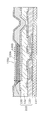
- FIG. 1 is a diagram showing the configuration of the organic EL element in the first embodiment.
- FIG. 2 is a cross-sectional view of a portion corresponding to one pixel in the organic EL constituent layer.
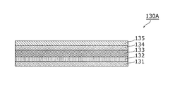
- FIG. 3 is a cross-sectional view showing an example of the configuration of the organic layer.
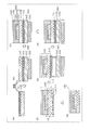
- FIG. 4 is a diagram for explaining a method of manufacturing the organic EL element in the first embodiment.
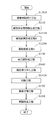
- FIG. 5 is a flowchart showing an example of a method for manufacturing an organic EL element in the first embodiment.
- FIG. 6 is a diagram for explaining a method of manufacturing an organic EL element in the second embodiment.
- FIG. 7 is a flowchart showing an example of a method for manufacturing an organic EL element in the second embodiment.
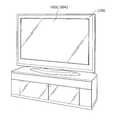
- FIG. 8 is an external view of a display device including an organic EL element.
- a method of manufacturing an organic electroluminescence (EL) element including a flexible substrate includes a step of forming a magnetic layer on at least a part of a surface of the flexible substrate, and the magnetic A step of temporarily holding the flexible substrate on which the body layer is formed on a non-flexible substrate having magnetism using a magnetic force, and an organic EL unit is formed on the temporarily held flexible substrate Forming a layer to be formed, separating the flexible substrate on which the layer constituting the organic EL portion is formed from the non-flexible substrate, and the flexible substrate separated from the non-flexible substrate. Separating the magnetic layer from a flexible substrate.
- the flexible substrate on which the magnetic layer is formed is temporarily held on the non-flexible substrate having magnetism using magnetic force. And the layer which comprises an organic EL element is formed on a flexible substrate. And the flexible substrate in which the layer which comprises an organic EL element was formed is isolate
- the flexible substrate is temporarily held on the non-flexible substrate by using magnetic force, it is extremely easy to separate the flexible substrate from the non-flexible substrate.
- the flexible substrate, the organic EL part formed on the flexible substrate, and the peripheral wiring are not damaged.
- the manufactured organic EL element since it has a step of removing the magnetic layer used for temporary holding, the manufactured organic EL element does not have a magnetic layer, and the physical characteristics of the magnetic layer are adversely affected. I do not receive it.
- the magnetic layer is formed of a resin containing magnetic particles.
- the flexible substrate is made of resin.
- the inflexible substrate includes a magnet layer.
- the inflexible substrate further includes a glass substrate layer.
- the layer constituting the organic EL part includes at least one of an active element layer, a planarization insulating layer, and an organic EL layer.
- At least a part of the magnetic layer is dissolved using a solvent.
- the method for manufacturing an organic EL element further includes the step of forming an adhesive layer on a part of the surface of the flexible substrate, and the flexible substrate on the non-flexible substrate. And a step of removing a portion where the flexible substrate and the non-flexible substrate are fixed via the adhesive layer, and a magnetic body on the surface of the flexible substrate.
- the magnetic layer is formed on the surface of the flexible substrate other than the portion where the adhesive layer is formed, and the flexible substrate is formed on the flexible substrate.
- the step of fixing to the non-flexible substrate through the adhesive layer is performed at the same time as or before and after the step of temporarily holding the flexible substrate on the non-flexible substrate using magnetic force,
- the flexible substrate and the non-flexible substrate are fixed via the adhesive layer. Removing the portion is the flexible substrate is carried out step and simultaneously or before the separating from the non-flexible substrate.
- FIG. 1 is a diagram illustrating a configuration of an organic EL element 100 according to the first embodiment.
- the organic EL element 100 is a display panel that can be bent freely. That is, the organic EL element 100 is a flexible display panel.
- FIG. 1A is a cross-sectional view of the organic EL element 100.
- FIG. 1B is a perspective view of a part of the organic EL element 100.
- the organic EL element 100 is an active matrix display panel.
- the organic EL element 100 may be a passive matrix display panel.
- the organic EL element 100 is an organic EL panel using an organic EL (Electro-Luminescence) element.
- the organic EL element 100 is a top emission type panel.
- the organic EL element 100 may be a bottom emission type panel.
- the organic EL element 100 includes a flexible substrate 110, an organic EL component layer 210, a sealing layer 140, and a sealing member 150.
- the flexible substrate 110 is a substrate that can be bent freely. That is, the flexible substrate 110 is a flexible substrate.
- the flexible substrate 110 is a resin substrate whose main component is polyimide. That is, the flexible substrate 110 is made of resin.
- the material constituting the flexible substrate 110 is not limited to polyimide.
- the material constituting the flexible substrate 110 may be, for example, triacetyl cellulose, polyethersulfone (PES), polyethylene terephthalate (PET), polyethylene naphthalate (PEN), or the like.
- the flexible substrate 110 may be formed of a plurality of types of materials.
- the organic EL constituent layer 210 is a layer constituting the organic EL part.
- the organic EL unit is, for example, an organic light emitting diode.
- the organic EL constituent layer 210 is formed on the flexible substrate 110.
- the organic EL component layer 210 functions as a display unit for displaying an image.
- the organic EL constituent layer 210 includes an active element layer 120, an organic EL layer 130, and a planarization insulating layer (not shown).
- the active element layer 120 is a layer in which an active element such as a TFT (thin film transistor) is formed.
- the active element layer 120 is formed on the flexible substrate 110.
- the TFTs 121 are arranged in a matrix.
- the organic EL layer 130 is a layer that emits light.
- FIG. 2 is a cross-sectional view of a portion corresponding to one pixel in the organic EL constituent layer 210. 2 shows the flexible substrate 110 that is not included in the organic EL component layer 210 for the sake of explanation.
- the organic EL constituent layer 210 includes an active element layer 120, an organic EL layer 130, and a planarization insulating layer 122. That is, the organic EL constituent layer 210 includes at least one of the active element layer 120, the planarization insulating layer 122, and the organic EL layer 130.
- the planarization insulating layer 122 is a layer that electrically insulates the active element layer 120 and the organic EL layer 130.
- the organic EL layer 130 includes an upper electrode 130U, an organic layer 130A, and a lower electrode 130D.
- the organic layer 130A is formed between the upper electrode 130U and the lower electrode 130D.
- the upper electrode 130U and the lower electrode 130D are a cathode and an anode, respectively.
- the lower electrode 130D is an electrode having light reflectivity and is formed on the planarization insulating layer 122.
- the upper electrode 130U is a transparent electrode having optical transparency, and is formed on the organic layer 130A.
- the upper electrode 130U and the lower electrode 130D may be an anode and a cathode, respectively.
- a light emitting portion is formed by the upper electrode 130U, the organic layer 130A, and the lower electrode 130D.
- the light emitting unit is an organic EL unit.
- the organic EL layer 130 a plurality of organic EL portions arranged in a matrix are formed.
- FIG. 3 is a cross-sectional view showing an example of the configuration of the organic layer 130A.
- the organic layer 130 ⁇ / b> A includes a hole injection layer 131, a hole transport layer 132, a light emitting layer 133, an electron transport layer 134, and an electron injection layer 135.
- the hole injection layer 131 is a layer mainly composed of a hole injecting material, and is formed on the lower electrode 130D.
- the hole transport layer 132 is a layer mainly composed of a hole transport material and is formed on the hole injection layer 131.
- the light emitting layer 133 is a layer mainly composed of an organic light emitting material that emits light by recombination of holes and electrons, and is formed on the hole transport layer 132.
- the electron transport layer 134 is a layer mainly composed of an electron transport material and is formed on the light emitting layer 133.
- the electron injection layer 135 is formed on the electron transport layer 134.
- the configuration of the organic layer 130A is not limited to the configuration shown in FIG. 3.
- the organic layer 130A includes the hole injection layer 131, the hole transport layer 132, the light emitting layer 133, and the electron transport layer 134. May be configured.
- the sealing layer 140 is formed on the organic EL layer 130, and the sealing member 150 is formed on the sealing layer 140.
- the sealing member 150 is a member for preventing moisture, oxygen, and the like in the outside air from entering.
- FIG. 4 is a diagram for explaining a method of manufacturing the organic EL element 100 according to the first embodiment.
- FIG. 5 is a flowchart showing an example of a method for manufacturing the organic EL element 100 according to the first embodiment.
- the magnetic substance-containing resin is a resin containing magnetic particles.
- magnetic particles and resin are used.
- the main material of the magnetic particles is ferrite, iron sand and the like.
- the main material constituting the resin is soluble polyimide.
- the magnetic substance-containing resin 111 shown in FIG. 4A is produced by dispersing the magnetic substance particles in the resin.
- the magnetic substance-containing resin 111 is a magnetic substance layer. That is, the magnetic substance-containing resin 111 as the magnetic substance layer is formed of a resin containing magnetic particles.
- a magnetic layer forming step is performed (S111).
- a magnetic body-containing resin 111 as a magnetic layer is applied to the surface of the flexible substrate 110.
- the magnetic substance-containing resin 111 is cured by using ultraviolet rays (UV) or the like. That is, the magnetic layer forming step is a step of forming a magnetic layer (magnetic substance-containing resin 111) on the surface of the flexible substrate 110.
- the flexible substrate 110 having a magnetic layer (magnetic material-containing resin 111) formed on the surface is also referred to as a magnetic layer forming substrate.
- a substrate fixing step is performed (S120).
- the magnetic layer forming substrate is fixed to the inflexible substrate 300 using magnetic force.
- the non-flexible substrate 300 is a substrate that does not have flexibility.
- the non-flexible substrate 300 includes a support substrate 310 and a magnet 320.
- the magnet 320 is an inflexible magnet.
- the magnet 320 constitutes a magnet layer. That is, the non-flexible substrate 300 includes a magnet layer.
- the non-flexible substrate 300 is a substrate in which a support substrate 310 is placed on top of a magnet 320. That is, the inflexible substrate 300 is a substrate having magnetism.
- the support substrate 310 is an inflexible substrate.
- a main material constituting the support substrate 310 is glass. That is, the support substrate 310 constitutes a glass substrate layer. That is, the inflexible substrate 300 includes a glass substrate layer.
- the material which comprises the support substrate 310 is not limited to glass, Ceramics, silicon, etc. may be sufficient.
- one of the support substrate 310 and the magnet 320 may be flexible, and the other of the support substrate 310 and the magnet 320 may be inflexible.
- the inflexible substrate 300 is fixed to the lower portion of the inverted magnetic layer forming substrate.
- the inverted magnetic layer forming substrate is a substrate in which a flexible substrate 110 is provided on top of the magnetic substance-containing resin 111 as shown in FIG. By fixing the non-flexible substrate 300 to the lower portion of the inverted magnetic layer forming substrate, the flexible substrate 110 does not bend.
- the non-flexible substrate 300 is fixed to the lower portion of the inverted magnetic layer forming substrate by the coupling force generated by the magnetic force of the magnetic substance-containing resin 111 and the magnetic force of the magnet 320 of the non-flexible substrate 300. Is done. That is, no adhesive or the like is used on the surface where the support substrate 310 and the magnetic substance-containing resin 111 are in close contact.
- the support substrate 310 and the magnet 320 are not bonded to each other by an adhesive or the like, the coupling caused by the magnetic force of the magnetic substance-containing resin 111 and the magnetic force of the magnet 320 of the non-flexible substrate 300.
- the magnet 320 is fixed to the support substrate 310 by the force.
- the substrate fixing step is a step of temporarily holding the flexible substrate 110 on which the magnetic layer (magnetic material-containing resin 111) is formed on the non-flexible substrate 300 having magnetism using a magnetic force.
- a display part forming step is performed (S130).
- an organic EL constituent layer 210 as a display part is formed.
- the active element layer 120, the planarization insulating layer 122, and the organic EL layer 130 in FIG. 2 are stacked in this order on the flexible substrate 110.
- the flexible substrate 110 is on the surface of the flexible substrate 110 where the magnetic substance-containing resin 111 is not formed.
- the organic EL constituent layer 210 is formed on the flexible substrate 110 (see FIG. 4C).
- the organic EL constituent layer 210 is formed on the flexible substrate 110 temporarily held by the magnet 320.
- sealing layer 140 is formed so that the organic EL structure layer 210 may be covered as FIG.4 (c) shows.
- a sealing member 150 is formed on the sealing layer 140.
- the organic EL element 100 is formed on the magnetic substance-containing resin 111.
- a magnet removal process is performed (S140).
- the magnet 320 fixed to the support substrate 310 by the magnetic force is removed from the support substrate 310. Therefore, the magnetic substance-containing resin 111 and the support substrate 310 can be easily separated.
- the organic EL element 100 in which the magnetic substance-containing resin 111 is formed in the lower portion is separated from a part of the support substrate 310 of the non-flexible substrate 300. .
- the organic EL element 100 includes a flexible substrate 110.
- the substrate separation step is a step of separating the flexible substrate 110 on which the organic EL component layer 210 is formed from the non-flexible substrate 300.
- a resin removal step is performed (S160).
- the magnetic substance-containing resin 111 is dissolved by applying the magnetic substance-containing resin 111 to the solvent 10 as shown in FIG.
- the solvent 10 is DMF (dimethylformamide).
- the magnetic substance-containing resin 111 can be dissolved by a method such as washing away with the solvent 10 in addition to the method of attaching to the solvent 10.
- the resin removing step is a step of separating the magnetic body-containing resin 111 as a magnetic layer from the flexible substrate 110 separated from the non-flexible substrate 300.
- the solvent 10 is not limited to DMF, and may be any other solvent as long as it can dissolve the magnetic substance-containing resin 111.
- the production of the organic EL element 100 is completed by the resin removing step (see FIG. 4G).
- the non-flexible substrate 300 is fixed to the lower part of the magnetic layer forming substrate including the flexible substrate 110 using the magnetic force. , Will not bend.
- the organic EL constituent layer 210 is formed on the flexible substrate 110. Therefore, the organic EL constituent layer 210 can be formed on the flexible substrate 110 with high accuracy.
- the magnet 320 is removed from the support substrate 310. Then, the magnetic substance-containing resin 111 and the support substrate 310 are separated. And the magnetic body containing resin 111 is melt
- the organic EL element can be manufactured without damaging the flexible substrate, the organic EL portion formed on the flexible substrate, and the peripheral wiring.
- the manufactured organic EL element does not have the magnetic layer used for temporary holding, it is not affected by the physical characteristics of the magnetic layer.
- the organic EL element manufactured by the manufacturing method of the present embodiment is the organic EL element 100 in FIG.
- FIG. 6 is a diagram for explaining a method of manufacturing the organic EL element 100 according to the second embodiment.
- FIG. 7 is a flowchart showing an example of a method for manufacturing the organic EL element 100 according to the second embodiment.
- the process with the same step number as the step number of FIG. 5 is performed in the same way as the process described in the first embodiment, and therefore detailed description will not be repeated.
- an adhesive material pasting step is performed (S101A).
- an adhesive 112 as an adhesive layer is provided at the end of the surface of the flexible substrate 110 as shown in FIG. That is, the adhesive 112 as an adhesive layer is formed at the end of the surface of the flexible substrate 110.
- the main material of the adhesive 112 is silicone.
- an adhesive 112 as an adhesive layer is formed on a part of the surface of the flexible substrate 110.
- the material of the adhesive 112 is not limited to silicone, and may be other materials as long as the material is used for bonding.
- a magnetic substance-containing resin generation step is performed (S110).
- the same processing as in the first embodiment is performed, and thus detailed description will not be repeated.
- the magnetic substance-containing resin 111 is generated.
- a magnetic layer forming step A is performed (S111A).
- a magnetic layer is formed on the surface of the flexible substrate 110 other than the portion where the adhesive layer (adhesive 112) is formed.
- the magnetic body-containing resin 111 is applied.
- the magnetic substance-containing resin 111 is cured by using ultraviolet rays (UV) or the like. That is, the magnetic layer (magnetic substance-containing resin) is formed on the surface of the flexible substrate 110 other than the portion where the adhesive layer (adhesive 112) is formed in the surface of the flexible substrate 110 by the magnetic layer formation step A. 111) is formed.
- UV ultraviolet rays
- a substrate fixing step A is performed (S120A).
- the magnetic layer forming substrate is fixed (bonded) to the non-flexible substrate 300.
- the magnetic layer forming substrate is a flexible substrate 110 having a magnetic layer (magnetic material-containing resin 111) formed on the surface thereof.
- the substrate fixing step A is a step of fixing the flexible substrate 110 to the non-flexible substrate 300 through the adhesive layer (adhesive 112).
- the flexible substrate 110 on which the magnetic layer (magnetic material-containing resin 111) is formed is temporarily held on the non-flexible substrate 300 having magnetism using magnetic force. That is, the substrate fixing step A and the substrate fixing step of FIG. 5 are performed simultaneously.
- the substrate fixing step A may be performed before or after the substrate fixing step. That is, the substrate fixing step A is performed simultaneously with or before or after the substrate fixing step.
- a display part forming step is performed (S130).
- the same processing as that in the first embodiment is performed, and thus detailed description will not be repeated.
- the organic EL constituent layer 210, the sealing layer 140, and the sealing member 150 are formed on the flexible substrate 110.
- the flexible substrate 110 is on the surface of the flexible substrate 110 where the magnetic substance-containing resin 111 is not formed.
- the organic EL constituent layer 210 is formed above the magnetic substance-containing resin 111. That is, the organic EL component layer 210 is formed above the surface of the flexible substrate 110 other than the portion where the adhesive layer (adhesive 112) is formed on the surface of the flexible substrate 110.
- a cutting process is performed (S141A).
- the cutting lines CL1 and CL2 shown in FIG. 6E are cut using a cutting member such as a cutter.
- the cutting lines CL1 and CL2 are provided outside the organic EL constituent layer 210 and inside the adhesive layer (adhesive 112) as shown in FIG. 6 (e).
- the cutting lines CL1 and CL2 are provided upward from the surface of the support substrate 310.
- the cutting lines CL1 and CL2 are provided upward from the bottom of the magnetic substance-containing resin 111 so as not to touch the surface of the support substrate 310 and to be able to cut a part of the magnetic substance-containing resin 111. Also good.
- the organic EL element 100 in which the magnetic substance-containing resin 111 is formed in the lower portion As shown in FIG.
- the organic EL element 100 in which the magnetic substance-containing resin 111 is formed in the lower portion shown in FIG. 6F is referred to as a magnetic substance-containing resin holding panel.
- the cutting step is a step of removing a portion where the flexible substrate 110 and the non-flexible substrate 300 are fixed via the adhesive layer.
- a substrate separation step is performed (S150).
- the magnetic body-containing resin holding panel is separated from a part of the support substrate 310 of the non-flexible substrate 300 as shown in FIG.
- the cutting step is not limited to being performed before the substrate separation step, and may be performed simultaneously with the substrate separation step. That is, the cutting process is performed simultaneously with or before the substrate separation process.
- a resin removal step is performed (S160).
- the same processing as that in the first embodiment is performed, and thus detailed description will not be repeated (see FIG. 6G).
- the production of the organic EL element 100 is completed by the resin removal step (see FIG. 6 (h)).
- the non-flexible substrate 300 is fixed to the lower part of the magnetic layer forming substrate including the flexible substrate 110 using the magnetic force. , Will not bend.
- the organic EL constituent layer 210 is formed on the flexible substrate 110. Therefore, the organic EL constituent layer 210 can be formed on the flexible substrate 110 with high accuracy.
- the organic EL constituent layer 210 is formed, the magnetic substance-containing resin 111 and the support substrate 310 are separated. And the magnetic body containing resin 111 is melt
- an organic EL element can be manufactured without damaging the flexible substrate, the organic EL portion formed on the flexible substrate, and the peripheral wiring, and the manufactured organic EL element has a magnetic layer. It is not affected by the physical characteristics of
- the flexible substrate can be held more reliably.
- FIG. 8 is an external view of a display device 1000 including the organic EL element 100 or the organic EL element 100A.
- the present invention does not damage the flexible substrate, the organic EL portion formed on the flexible substrate, and the peripheral wiring in the manufacturing process of the organic EL element including the flexible substrate, and the manufactured organic EL device. It can be used as a method for producing an organic EL element in which the EL element is not affected by the physical characteristics of the magnetic layer.
Landscapes
- Engineering & Computer Science (AREA)
- Manufacturing & Machinery (AREA)
- Physics & Mathematics (AREA)
- Optics & Photonics (AREA)
- Electroluminescent Light Sources (AREA)
Abstract
磁性体含有樹脂(111)が形成された可撓性基板(110)を、磁性を有する非可撓性基板(300)に磁力を用いて仮保持させる。可撓性基板(110)の上に、有機EL構成層(210)が形成される。有機EL構成層(210)が形成された可撓性基板(110)が、非可撓性基板(300)から分離される。可撓性基板(110)に形成された磁性体含有樹脂(111)が分離される。
Description
本発明は、可撓性基板を備える有機EL(Electro Luminescence)素子の製造方法に関する。
近年、自由に曲げることが可能なディスプレイとして、フレキシブルディスプレイが注目されている。フレキシブルディスプレイは、有機発光ダイオード等の有機EL(Electro Luminescence)部を用いたものが主流である。
フレキシブルディスプレイの製造では、自由に曲げることが可能な可撓性基板上に、有機EL部等を形成する必要がある。可撓性基板上に有機EL部を形成する手法の一つとして、可撓性基板にガラス等の非可撓性基板を接着剤等で接着した状態で、可撓性基板上に有機EL部を形成する手法がある。
この手法では、有機EL部を形成した後、可撓性基板と非可撓性基板とを分離する際、接着力を上回る力で可撓性基板を非可撓性基板から引き剥がす必要があるため、可撓性基板が損傷したり、可撓性基板上に形成された有機EL部が破壊してしまう可能性がある。
そこで、上記問題を解決するために、特許文献1には、磁性膜が形成されたフレキシブル基板(可撓性基板)を、磁力によって基板ホルダ(非可撓性基板)に仮固定する技術(以下、従来技術Aという)が開示されている。
しかしながら、従来技術Aでは、可撓性基板と非可撓性基板とを分離させた後においても、磁性膜が可撓性基板に残存した構成となされているため、完成したフレキシブル素子は当該磁性膜の物理的特性の影響を受けたものになってしまう。
すなわち、磁性膜の膜厚や、磁性膜を構成する磁性材料の組成によっては、曲げ強度が低下して割れ易くなると共に、透明性が低下してしまうため、完成したフレキシブル素子のフレキシブル性が低下してしまうと共に、発光の取出し側が制約されてしまうという問題が生じる。
また、フレキシブル基板が薄く形成された場合、フレキシブル基板の一方の面に形成される磁性膜と、フレキシブル基板の他方の面に形成されるTFT(Thin film transistor)電極との距離が短くなる。この場合、層間容量が生じ、ノイズや信号遅延の原因となる。
また、フレキシブル基板を用いて構成されたフレキシブルディスプレイが、端末のディスプレイ部として筐体内に組込まれた構成において、磁性膜の膜剥れが生じると、当該磁性膜が筐体内の電子部品と接触し、誤動作、発熱、発火などの要因となり得る。
さらに、非可撓性基板から磁性膜を分離した後、残存した磁性膜の膜応力によって可撓性基板が湾曲してしまい、完成したフレキシブル素子の平坦性を確保することが困難になるという問題も生じる。
本発明は、上述の問題点を解決するためになされたものであって、その目的は、可撓性基板を備える有機EL素子の製造過程において、可撓性基板、可撓性基板上に形成された有機EL部ならびに周辺配線を損傷させることがないと共に、仮固定に用いた磁性膜の物理的特性の悪影響を受けることがない有機EL素子の製造方法を提供することである。
上述の課題を解決するために、この発明のある局面に従うと、可撓性基板を備えた有機エレクトロルミネッセンス(EL)素子の製造方法は、前記可撓性基板の表面の少なくとも一部に磁性体層を形成するステップと、前記磁性体層が形成された前記可撓性基板を、磁性を有する非可撓性基板に磁力を用いて仮保持するステップと、前記仮保持された可撓性基板の上に、有機EL部を構成する層を形成するステップと、前記有機EL部を構成する層が形成された可撓性基板を、前記非可撓性基板から分離するステップと、前記非可撓性基板から分離された前記可撓性基板から前記磁性体層を分離するステップとを含む。
本発明により、可撓性基板を備える有機EL素子の製造過程において、可撓性基板、可撓性基板上に形成された有機EL部ならびに周辺配線を損傷させることがないと共に、磁性膜の物理的特性の悪影響を受けることがない有機EL素子を製造することができる。
本発明のある局面に従うと、可撓性基板を備えた有機エレクトロルミネッセンス(EL)素子の製造方法は、前記可撓性基板の表面の少なくとも一部に磁性体層を形成するステップと、前記磁性体層が形成された前記可撓性基板を、磁性を有する非可撓性基板に磁力を用いて仮保持するステップと、前記仮保持された可撓性基板の上に、有機EL部を構成する層を形成するステップと、前記有機EL部を構成する層が形成された可撓性基板を、前記非可撓性基板から分離するステップと、前記非可撓性基板から分離された前記可撓性基板から前記磁性体層を分離するステップとを含む。
本態様によると、磁性体層が形成された可撓性基板を、磁性を有する非可撓性基板に磁力を用いて仮保持させる。そして、可撓性基板の上に、有機EL素子を構成する層が形成される。そして、有機EL素子を構成する層が形成された可撓性基板が、前記非可撓性基板から分離される。
本発明では、磁力を用いて可撓性基板が非可撓性基板に仮保持されるため、可撓性基板と非可撓性基板との分離が極めて容易であり、接着剤を用いた場合のように可撓性基板、可撓性基板上に形成された有機EL部や周辺配線を損傷させることがない。
さらに、本発明では、仮保持に用いた磁性体層を除去する工程を有するため、製造された有機EL素子は磁性体層を保有しておらず、当該磁性体層の物理的特性の悪影響を受けることがない。
また、好ましくは、前記磁性体層は、磁性体粒子を含む樹脂で形成されている。
また、好ましくは、前記可撓性基板は、樹脂で形成されている。
また、好ましくは、前記非可撓性基板は、磁石層を含む。
また、好ましくは、前記非可撓性基板は、さらに、ガラス基板層を含む。
また、好ましくは、前記有機EL部を構成する層が、アクティブ素子層、平坦化絶縁層、有機EL層の内の少なくとも一つを含む。
また、好ましくは、前記可撓性基板から前記磁性体層を分離するステップにおいて、該磁性体層の少なくとも一部を溶剤を用いて溶解させる。
また、好ましくは、有機EL素子の製造方法は、さらに、前記可撓性基板の表面の一部に接着層を形成するステップと、前記可撓性基板を前記非可撓性基板に前記接着層を介して固定するステップと、前記可撓性基板と前記非可撓性基板とが前記接着層を介して固定された部分を除去するステップとを含み、前記可撓性基板の表面に磁性体層を形成するステップでは、前記可撓性基板の表面のうち、前記接着層が形成された部分以外の前記可撓性基板の表面に前記磁性体層が形成され、前記可撓性基板を前記非可撓性基板に前記接着層を介して固定するステップは、前記可撓性基板を前記非可撓性基板に磁力を用いて仮保持するステップと同時若しくはその前後に行われ、前記可撓性基板と前記非可撓性基板とが前記接着層を介して固定された部分を除去するステップは、前記可撓性基板を、前記非可撓性基板から分離するステップと同時若しくはその前に行われる。
以下、図面を参照しつつ、本発明の実施の形態に係る表示パネル装置および表示装置について説明する。以下の説明では、同一の部品には同一の符号を付してある。それらの名称および機能も同じである。したがって、それらについての詳細な説明は繰り返さない。また、図面は説明のために一部を強調するなどデフォルメすることがあり、必ずしも図面に現れる比率が正しいとは限らない。
<第1の実施の形態>
図1は、第1の実施の形態における有機EL素子100の構成を示す図である。有機EL素子100は、自由に曲げることが可能な表示パネルである。すなわち、有機EL素子100は、可撓性を有する表示パネルである。
図1は、第1の実施の形態における有機EL素子100の構成を示す図である。有機EL素子100は、自由に曲げることが可能な表示パネルである。すなわち、有機EL素子100は、可撓性を有する表示パネルである。
図1(a)は、有機EL素子100の断面図である。図1(b)は、有機EL素子100の一部の斜視図である。
有機EL素子100は、アクティブマトリクス方式の表示パネルである。なお、有機EL素子100は、パッシブマトリクス方式の表示パネルであってもよい。有機EL素子100は、有機EL(Electro Luminescence)素子を使用した有機ELパネルである。有機EL素子100は、トップエミッション方式のパネルである。なお、有機EL素子100は、ボトムエミッション方式のパネルであってもよい。
図1(a)に示されるように、有機EL素子100は、可撓性基板110と、有機EL構成層210と、封止層140と、封止部材150とを含む。
可撓性基板110は、自由に曲げることが可能な基板である。すなわち、可撓性基板110は、可撓性を有する基板である。可撓性基板110は、ポリイミドを主成分とする樹脂基板である。すなわち、可撓性基板110は、樹脂で形成される。
なお、可撓性基板110を構成する材料は、ポリイミドに限定されない。可撓性基板110を構成する材料は、例えば、トリアセチルセルロース、ポリエーテルサルフォン(PES)、ポリエチレンテレフタレート(PET)、ポリエチレンナフタレート(PEN)等であってもよい。また、可撓性基板110は、複数種類の材料により形成されてもよい。
有機EL構成層210は、有機EL部を構成する層である。有機EL部は、例えば、有機発光ダイオードである。有機EL構成層210は、可撓性基板110上に形成される。有機EL構成層210は、画像を表示するための表示部として機能する。
有機EL構成層210は、アクティブ素子層120と、有機EL層130と、図示しない平坦化絶縁層とを含む。
アクティブ素子層120は、TFT(Thin film transistor)等のアクティブ素子が形成される層である。アクティブ素子層120は、可撓性基板110の上部に形成される。図1(b)に示されるように、TFT121は、行列状に配置される。
有機EL層130は、光を発する層である。
図2は、有機EL構成層210のうち、1つの画素に対応する部分の断面図である。なお、図2には、説明のために、有機EL構成層210に含まれない可撓性基板110が示される。
有機EL構成層210は、アクティブ素子層120と、有機EL層130と、平坦化絶縁層122とを含む。つまり、有機EL構成層210は、アクティブ素子層120、平坦化絶縁層122および有機EL層130の内の少なくとも一つを含む。
平坦化絶縁層122は、アクティブ素子層120と、有機EL層130とを電気的に絶縁する層である。
有機EL層130は、上部電極130Uと、有機層130Aと、下部電極130Dとを含む。有機層130Aは、上部電極130Uと下部電極130Dとの間に形成される。
上部電極130Uおよび下部電極130Dは、それぞれ、陰極および陽極である。
下部電極130Dは、光反射性を有する電極であり、平坦化絶縁層122上に形成される。上部電極130Uは、光透過性を有する透明電極であり、有機層130A上に形成される。
なお、上部電極130Uおよび下部電極130Dは、それぞれ、陽極および陰極であってもよい。
上部電極130Uと、有機層130Aと、下部電極130Dとにより発光部が形成される。当該発光部は、有機EL部である。有機EL層130には、行列状に配置される複数の有機EL部が形成される。
図3は、有機層130Aの構成の一例を示す断面図である。
図3を参照して、有機層130Aは、正孔注入層131と、正孔輸送層132と、発光層133と、電子輸送層134と、電子注入層135とを含む。
正孔注入層131は、正孔注入性の材料を主成分とする層であり、下部電極130D上に形成される。正孔輸送層132は、正孔輸送性の材料を主成分とする層であり、正孔注入層131上に形成される。
発光層133は、正孔と電子とが再結合することにより発光する有機発光材料を主成分とする層であり、正孔輸送層132上に形成される。
電子輸送層134は、電子輸送性の材料を主成分とする層であり、発光層133上に形成される。電子注入層135は、電子輸送層134上に形成される。
なお、有機層130Aの構成は、図3に示される構成に限定されず、例えば、有機層130Aは、正孔注入層131と、正孔輸送層132と、発光層133と、電子輸送層134とから構成されてもよい。
再び、図1(a)および図1(b)を参照して、有機EL層130の上部には、封止層140が形成され、封止部材150が、封止層140上に形成される。封止部材150は、外気中の水分や酸素などが浸入するのを防止するための部材である。
(有機EL素子の製造方法)
次に、有機EL素子100の製造方法について説明する。
次に、有機EL素子100の製造方法について説明する。
図4は、第1の実施の形態における、有機EL素子100の製造方法を説明するための図である。
図5は、第1の実施の形態における、有機EL素子100の製造方法の一例を示すフローチャートである。
なお、以下で説明する各工程は周知のプロセス技術を用いて実施できるため、プロセス条件などの詳細な説明は適宜省略する。また、以下で示す材料およびプロセスは1つの典型例であって、本発明の有機EL素子およびその製造方法を限定するものではない。適性が知られている他の材料およびプロセスを代用した場合も本発明に含まれる。これらのことは、後述する第2の実施の形態における製造方法についても同様である。
まず、磁性体含有樹脂生成工程が行われる(S110)。磁性体含有樹脂とは、磁性体粒子を含む樹脂である。磁性体含有樹脂生成工程では、磁性体粒子および樹脂が使用される。当該磁性体粒子の主な材料は、フェライト、砂鉄等である。当該樹脂を構成する主な材料は、一例として、可溶性ポリイミドである。
磁性体含有樹脂生成工程では、磁性体粒子を樹脂中に分散させることにより、図4(a)に示される磁性体含有樹脂111が生成される。磁性体含有樹脂111は、磁性体層である。すなわち、磁性体層としての磁性体含有樹脂111は、磁性体粒子を含む樹脂で形成される。
次に、磁性体層形成工程が行われる(S111)。磁性体層形成工程では、図4(a)に示されるように、可撓性基板110の表面に、磁性体層としての磁性体含有樹脂111が塗布される。
そして、紫外線(UV)等を使用することにより、磁性体含有樹脂111が硬化される。すなわち、磁性体層形成工程は、可撓性基板110の表面に磁性体層(磁性体含有樹脂111)を形成する工程である。以下においては、表面に磁性体層(磁性体含有樹脂111)が形成された可撓性基板110を、磁性体層形成基板ともいう。
次に、基板固定工程が行われる(S120)。基板固定工程では、非可撓性基板300に、磁性体層形成基板が磁力を用いて固定される。非可撓性基板300は、可撓性を有さない基板である。
図4(b)に示されるように、非可撓性基板300は、支持基板310と、磁石320とを含む。磁石320は、非可撓性の磁石である。磁石320は、磁石層を構成する。すなわち、非可撓性基板300は、磁石層を含む。
図4(b)に示されるように、非可撓性基板300は、磁石320の上部に支持基板310を載せた基板である。すなわち、非可撓性基板300は、磁性を有する基板である。
支持基板310は、非可撓性の基板である。支持基板310を構成する主な材料は、ガラスである。すなわち、支持基板310は、ガラス基板層を構成する。つまり、非可撓性基板300は、ガラス基板層を含む。
なお、支持基板310を構成する材料は、ガラスに限定されず、セラミックス、シリコン等であってもよい。
なお、支持基板310および磁石320の一方が可撓性を有し、支持基板310および磁石320の他方が非可撓性を有していてもよい。
具体的には、基板固定工程では、図4(b)に示されるように、反転させた磁性体層形成基板の下部に非可撓性基板300が固定される。
当該反転させた磁性体層形成基板は、図4(b)に示されるように、磁性体含有樹脂111の上部に可撓性基板110が設けられる基板である。反転させた磁性体層形成基板の下部に非可撓性基板300が固定されることにより、可撓性基板110は、撓まないようになる。
なお、磁性体含有樹脂111の有する磁力と、非可撓性基板300の磁石320の有する磁力とにより生じる結合力により、反転させた磁性体層形成基板の下部に非可撓性基板300が固定される。すなわち、支持基板310と磁性体含有樹脂111とが密着する面には、接着材等が使用されていない。
この場合、支持基板310と磁石320とは接着剤等により互いに貼り合わせられていなくても、磁性体含有樹脂111の有する磁力と、非可撓性基板300の磁石320の有する磁力とにより生じる結合力により、磁石320は支持基板310に固定される。
すなわち、基板固定工程は、磁性体層(磁性体含有樹脂111)が形成された可撓性基板110を、磁性を有する非可撓性基板300に磁力を用いて仮保持する工程である。
次に、表示部形成工程が行われる(S130)。表示部形成工程では、表示部としての有機EL構成層210が形成される。具体的には、表示部形成工程では、可撓性基板110上に、図2のアクティブ素子層120、平坦化絶縁層122、有機EL層130が、この順で積層される。ここで、可撓性基板110上とは、可撓性基板110において磁性体含有樹脂111が形成されていない側の面上である。
これにより、図2のように、可撓性基板110上に、有機EL構成層210が形成される((図4(c)参照))。
すなわち、磁石320により仮保持された可撓性基板110の上に、有機EL構成層210が形成される。
そして、図4(c)に示されるように、有機EL構成層210を覆うように封止層140が形成される。そして、封止層140の上部に封止部材150が形成される。
これにより、磁性体含有樹脂111上に、有機EL素子100が形成される。
次に、磁石取り外し工程が行われる(S140)。磁石取り外し工程では、図4(d)に示されるように、磁力により支持基板310に固定されている磁石320が、支持基板310から取り外される。したがって、磁性体含有樹脂111と支持基板310とは、容易に分離することができる。
そして、基板分離工程が行われる(S150)。基板分離工程では、図4(e)に示されるように、下部に磁性体含有樹脂111が形成される有機EL素子100が、非可撓性基板300の一部の支持基板310から分離される。有機EL素子100は、可撓性基板110を含む。
すなわち、基板分離工程は、有機EL構成層210が形成された可撓性基板110を、非可撓性基板300から分離する工程である。
次に、樹脂除去工程が行われる(S160)。樹脂除去工程では、図4(f)に示されるように、磁性体含有樹脂111を、溶剤10につけることにより、磁性体含有樹脂111を溶かす。溶剤10は、DMF(ジメチルホルムアミド)である。磁性体含有樹脂111は、溶剤10につける方法以外に、溶剤10により洗い流す等の方法によって、溶かすこともできる。
すなわち、磁性体層としての磁性体含有樹脂111の少なくとも一部は溶剤を用いて溶解される。つまり、樹脂除去工程は、非可撓性基板300から分離された可撓性基板110から磁性体層としての磁性体含有樹脂111を分離する工程である。
なお、溶剤10は、DMFに限定されることなく、磁性体含有樹脂111を溶かすことが可能な溶剤であれば他の溶剤であってもよい。
上記樹脂除去工程により、有機EL素子100の製造が終了する((図4(g)参照))。
以上、本実施の形態によれば、磁力を利用して、可撓性基板110を含む磁性体層形成基板の下部に非可撓性基板300が固定されることにより、可撓性基板110は、撓まないようになる。この状態で、可撓性基板110の上部に有機EL構成層210が形成される。したがって、高い精度で、可撓性基板110の上部に有機EL構成層210を形成することができる。
そして、有機EL構成層210が形成された後、磁石320が、支持基板310から取り外される。そして、磁性体含有樹脂111と支持基板310とが分離される。そして、磁性体含有樹脂111が溶解される。以上により、有機EL素子100が製造される。
したがって、可撓性基板、可撓性基板上に形成された有機EL部ならびに周辺配線を損傷させることなく、有機EL素子を製造することができる。
さらに、製造された有機EL素子は、仮保持に用いた磁性体層を有しないため、磁性体層の物理的特性の影響を受けることがない。
<第2の実施の形態>
本実施の形態では、磁力を利用すると共に、接着剤を使用した有機EL素子の製造方法について説明する。本実施の形態の製造方法により製造される有機EL素子は、図1(a)の有機EL素子100である。
本実施の形態では、磁力を利用すると共に、接着剤を使用した有機EL素子の製造方法について説明する。本実施の形態の製造方法により製造される有機EL素子は、図1(a)の有機EL素子100である。
(有機EL素子の製造方法)
次に、有機EL素子100の製造方法について説明する。
次に、有機EL素子100の製造方法について説明する。
図6は、第2の実施の形態における、有機EL素子100の製造方法を説明するための図である。
図7は、第2の実施の形態における、有機EL素子100の製造方法の一例を示すフローチャートである。図7において、図5のステップ番号と同じステップ番号の処理は、第1の実施の形態で説明した処理と同様な処理が行われるので詳細な説明は繰り返さない。
まず、接着材貼付け工程が行われる(S101A)。接着材貼付け工程では、図6(a)に示されるように、可撓性基板110の表面の端部に、接着層としての接着剤112が設けられる。すなわち、可撓性基板110の表面の端部に接着層としての接着剤112が形成される。接着剤112の主な材料は、シリコーンである。
すなわち、可撓性基板110の表面の一部に、接着層としての接着剤112が形成される。
なお、接着剤112の材料は、シリコーンに限定されず、接着の用途に使用される材料であれば、他の材料であってもよい。
なお、接着剤112が設けられる位置は、図6(a)に示される位置に限定されない。
次に、磁性体含有樹脂生成工程が行われる(S110)。磁性体含有樹脂生成工程では、第1の実施の形態と同様な処理が行なわれるので、詳細な説明は繰り返さない。この工程により、磁性体含有樹脂111が生成される。
次に、磁性体層形成工程Aが行われる(S111A)。磁性体層形成工程Aでは、図4(b)に示されるように、可撓性基板110の表面のうち、接着層(接着剤112)が形成された部分以外の表面に、磁性体層としての磁性体含有樹脂111が塗布される。
そして、紫外線(UV)等を使用することにより、磁性体含有樹脂111が硬化される。すなわち、磁性体層形成工程Aにより、可撓性基板110の表面のうち、接着層(接着剤112)が形成された部分以外の可撓性基板110の表面に磁性体層(磁性体含有樹脂111)が形成される。
次に、基板固定工程Aが行われる(S120A)。基板固定工程Aでは、非可撓性基板300に、磁性体層形成基板が固定される(貼り合わせられる)。磁性体層形成基板は、前述したように、表面に磁性体層(磁性体含有樹脂111)が形成された可撓性基板110である。
具体的には、基板固定工程Aでは、図6(c)に示されるように、反転させた磁性体層形成基板の下部に非可撓性基板300が接着層(接着剤112)により固定される。すなわち、基板固定工程Aは、可撓性基板110を非可撓性基板300に接着層(接着剤112)を介して固定する工程である。
なお、基板固定工程Aと同時に、磁性体層(磁性体含有樹脂111)が形成された可撓性基板110が、磁性を有する非可撓性基板300に磁力を用いて仮保持される。すなわち、基板固定工程Aと、図5の基板固定工程とは同時に行われる。
なお、基板固定工程Aは、基板固定工程の前または後に行われてもよい。つまり、基板固定工程Aは、基板固定工程と同時若しくはその前後に行われる。
次に、表示部形成工程が行われる(S130)。表示部形成工程では、第1の実施の形態と同様な処理が行われるので詳細な説明は繰り返さない。この工程により、図6(d)に示されるように、可撓性基板110上に、有機EL構成層210、封止層140および封止部材150が形成される。ここで、可撓性基板110上とは、可撓性基板110において磁性体含有樹脂111が形成されていない側の面上である。
なお、有機EL構成層210は、磁性体含有樹脂111の上方に形成される。すなわち、有機EL構成層210は、可撓性基板110の表面のうち、接着層(接着剤112)が形成された部分以外の可撓性基板110の表面の上方に形成される。
次に、磁石取り外し工程が行われる(S140)。磁石取り外し工程では、第1の実施の形態と同様な処理が行われるので詳細な説明は繰り返さない。
次に、切断工程が行われる(S141A)。切断工程では、カッター等の切断部材を用いて、図6(e)に示される切断線CL1,CL2の部分が切断される。
切断線CL1,CL2は、図6(e)に示されるように、有機EL構成層210の外部であって、かつ、接着層(接着剤112)の内部に設けられる。また、切断線CL1,CL2は、支持基板310の表面から上方に向かって設けられる。
なお、切断線CL1,CL2は、支持基板310の表面に触れず、かつ、磁性体含有樹脂111の一部を切断可能な程度に、磁性体含有樹脂111の下部から上方に向かって設けられてもよい。
切断工程により、図6(f)に示される、下部に磁性体含有樹脂111が形成される有機EL素子100が、支持基板310から分離可能な状態となる。以下においては、図6(f)に示される、下部に磁性体含有樹脂111が形成される有機EL素子100を、磁性体含有樹脂保持パネルという。
切断工程が行われる前は、磁性体含有樹脂保持パネルに含まれる可撓性基板110と、非可撓性基板300の一部の支持基板310とが接着層(接着剤112)により固定されている。したがって、切断工程は、可撓性基板110と非可撓性基板300とが接着層を介して固定された部分を除去する工程である。
次に、第1の実施の形態と同様に、基板分離工程が行われる(S150)。基板分離工程では、図6(f)に示されるように、磁性体含有樹脂保持パネルが、非可撓性基板300の一部の支持基板310から分離される。
なお、切断工程は、基板分離工程の前に行われることに限定されず、基板分離工程と同時に行われてもよい。すなわち、切断工程は、基板分離工程と同時若しくはその前に行なわれる。
次に、樹脂除去工程が行われる(S160)。樹脂除去工程では、第1の実施の形態と同様な処理が行われるので詳細な説明は繰り返さない((図6(g)参照))。
上記樹脂除去工程により、有機EL素子100の製造が終了する((図6(h)参照))。
以上、本実施の形態によれば、磁力を利用して、可撓性基板110を含む磁性体層形成基板の下部に非可撓性基板300が固定されることにより、可撓性基板110は、撓まないようになる。この状態で、可撓性基板110の上部に有機EL構成層210が形成される。したがって、高い精度で、可撓性基板110の上部に有機EL構成層210を形成することができる。
そして、有機EL構成層210が形成された後、磁性体含有樹脂111と支持基板310とが分離される。そして、磁性体含有樹脂111が溶解される。以上により、有機EL素子100が製造される。
したがって、本実施の形態においても、第1の実施の形態と同様な効果が得られる。すなわち、可撓性基板、可撓性基板上に形成された有機EL部ならびに周辺配線を損傷させることなく、有機EL素子を製造することができると共に、製造された有機EL素子は、磁性体層の物理的特性の影響を受けることがない。
さらに、第2の実施の形態においては、磁力に加えて接着剤を併用しているので、可撓性基板をより確実に保持することができる。
(表示装置の外観図)
図8は、有機EL素子100または有機EL素子100Aを備える表示装置1000の外観図である。
図8は、有機EL素子100または有機EL素子100Aを備える表示装置1000の外観図である。
以上、本発明における有機EL素子について、実施の形態に基づいて説明したが、本発明は、これらの実施の形態に限定されるものではない。本発明の趣旨を逸脱しない限り、当業者が思いつく各種変形を本実施の形態に施したもの、あるいは異なる実施の形態における構成要素を組み合わせて構築される形態も、本発明の範囲内に含まれる。
今回開示された実施の形態はすべての点で例示であって制限的なものではないと考えられるべきである。本発明の範囲は上記した説明ではなくて請求の範囲によって示され、請求の範囲と均等の意味および範囲内でのすべての変更が含まれることが意図される。
本発明は、可撓性基板を備える有機EL素子の製造過程において、可撓性基板、可撓性基板上に形成された有機EL部ならびに周辺配線を損傷させることがないと共に、製造された有機EL素子が磁性体層の物理的特性の影響を受けることがない、有機EL素子の製造方法として、利用することができる。
10 溶剤
100,100A 有機EL素子
110 可撓性基板
111 磁性体含有樹脂
112 接着剤
120 アクティブ素子層
121 TFT
122 平坦化絶縁層
130 有機EL層
130A 有機層
130D 下部電極
130U 上部電極
131 正孔注入層
132 正孔輸送層
133 発光層
134 電子輸送層
135 電子注入層
140 封止層
150 封止部材
210 有機EL構成層
300 非可撓性基板
310 支持基板
320 磁石
1000 表示装置
100,100A 有機EL素子
110 可撓性基板
111 磁性体含有樹脂
112 接着剤
120 アクティブ素子層
121 TFT
122 平坦化絶縁層
130 有機EL層
130A 有機層
130D 下部電極
130U 上部電極
131 正孔注入層
132 正孔輸送層
133 発光層
134 電子輸送層
135 電子注入層
140 封止層
150 封止部材
210 有機EL構成層
300 非可撓性基板
310 支持基板
320 磁石
1000 表示装置
Claims (8)
- 可撓性基板を備えた有機エレクトロルミネッセンス(EL)素子の製造方法であって、
前記可撓性基板の表面の少なくとも一部に磁性体層を形成するステップと、
前記磁性体層が形成された前記可撓性基板を、磁性を有する非可撓性基板に磁力を用いて仮保持するステップと、
前記仮保持された可撓性基板の上に、有機EL部を構成する層を形成するステップと、
前記有機EL部を構成する層が形成された可撓性基板を、前記非可撓性基板から分離するステップと、
前記非可撓性基板から分離された前記可撓性基板から前記磁性体層を分離するステップとを含む、
有機EL素子の製造方法。 - 前記磁性体層は、磁性体粒子を含む樹脂で形成されている、
請求項1に記載された有機EL素子の製造方法。 - 前記可撓性基板は、樹脂で形成されている、
請求項1又は請求項2に記載された有機EL素子の製造方法。 - 前記非可撓性基板は、磁石層を含む、
請求項1乃至請求項3のいずれか1項に記載された有機EL素子の製造方法。 - 前記非可撓性基板は、さらに、ガラス基板層を含む、
請求項4に記載された有機EL素子の製造方法。 - 前記有機EL部を構成する層が、アクティブ素子層、平坦化絶縁層、有機EL層の内の少なくとも一つを含む、
請求項1乃至請求項5のいずれか1項に記載された有機EL素子の製造方法。 - 前記可撓性基板から前記磁性体層を分離するステップにおいて、該磁性体層の少なくとも一部を溶剤を用いて溶解させる、
請求項1乃至請求項6のいずれか1項に記載された有機EL素子の製造方法。 - さらに、前記可撓性基板の表面の一部に接着層を形成するステップと、
前記可撓性基板を前記非可撓性基板に前記接着層を介して固定するステップと、
前記可撓性基板と前記非可撓性基板とが前記接着層を介して固定された部分を除去するステップとを含み、
前記可撓性基板の表面に磁性体層を形成するステップでは、前記可撓性基板の表面のうち、前記接着層が形成された部分以外の前記可撓性基板の表面に前記磁性体層が形成され、
前記可撓性基板を前記非可撓性基板に前記接着層を介して固定するステップは、前記可撓性基板を前記非可撓性基板に磁力を用いて仮保持するステップと同時若しくはその前後に行われ、
前記可撓性基板と前記非可撓性基板とが前記接着層を介して固定された部分を除去するステップは、前記可撓性基板を、前記非可撓性基板から分離するステップと同時若しくはその前に行われる、
請求項1に記載された有機EL素子の製造方法。
Priority Applications (1)
| Application Number | Priority Date | Filing Date | Title |
|---|---|---|---|
| US13/693,511 US8765503B2 (en) | 2010-07-16 | 2012-12-04 | Method for fabricating organic EL device |
Applications Claiming Priority (2)
| Application Number | Priority Date | Filing Date | Title |
|---|---|---|---|
| JP2010162152 | 2010-07-16 | ||
| JP2010-162152 | 2010-07-16 |
Related Child Applications (1)
| Application Number | Title | Priority Date | Filing Date |
|---|---|---|---|
| US13/693,511 Continuation US8765503B2 (en) | 2010-07-16 | 2012-12-04 | Method for fabricating organic EL device |
Publications (1)
| Publication Number | Publication Date |
|---|---|
| WO2012008166A1 true WO2012008166A1 (ja) | 2012-01-19 |
Family
ID=45469180
Family Applications (1)
| Application Number | Title | Priority Date | Filing Date |
|---|---|---|---|
| PCT/JP2011/004043 Ceased WO2012008166A1 (ja) | 2010-07-16 | 2011-07-15 | 有機el素子の製造方法 |
Country Status (2)
| Country | Link |
|---|---|
| US (1) | US8765503B2 (ja) |
| WO (1) | WO2012008166A1 (ja) |
Cited By (4)
| Publication number | Priority date | Publication date | Assignee | Title |
|---|---|---|---|---|
| WO2015008586A1 (ja) * | 2013-07-16 | 2015-01-22 | ソニー株式会社 | 基板の製造方法および電子デバイスの製造方法 |
| WO2017036102A1 (zh) * | 2015-09-06 | 2017-03-09 | 京东方科技集团股份有限公司 | 一种固定装置和蒸镀方法 |
| JP2020197678A (ja) * | 2019-06-05 | 2020-12-10 | 株式会社Joled | 表示装置および表示装置の製造方法 |
| CN119767948A (zh) * | 2024-12-31 | 2025-04-04 | 固安翌光科技有限公司 | 一种有机发光器件及装置 |
Families Citing this family (11)
| Publication number | Priority date | Publication date | Assignee | Title |
|---|---|---|---|---|
| JP6002135B2 (ja) | 2011-08-05 | 2016-10-05 | パナソニック株式会社 | フレキシブルデバイスの製造方法 |
| DE102014105020A1 (de) * | 2014-04-09 | 2015-10-15 | Von Ardenne Gmbh | Substratanordnung, Prozesskammer und Substrat |
| CN104993070A (zh) * | 2015-07-02 | 2015-10-21 | 深圳市华星光电技术有限公司 | 一种制作柔性oled显示器件的方法 |
| US10070520B2 (en) * | 2015-12-26 | 2018-09-04 | Intel Corporation | Magnetic particle embedded flex or printed flex for magnetic tray or electro-magnetic carrier |
| CN105428393B (zh) * | 2016-01-05 | 2019-10-18 | 京东方科技集团股份有限公司 | 一种柔性显示基板、柔性显示面板的制作方法及相关装置 |
| CN105552089B (zh) * | 2016-01-15 | 2018-09-07 | 京东方科技集团股份有限公司 | 基板结构及其柔性基板的贴附方法、剥离方法 |
| CN105679806B (zh) * | 2016-04-13 | 2018-07-17 | 京东方科技集团股份有限公司 | 柔性显示基板及其母板、制备方法、柔性显示面板及其母板 |
| CN107068906B (zh) * | 2017-04-28 | 2019-05-03 | 上海天马微电子有限公司 | 柔性显示面板及其制备方法和显示装置 |
| US10622579B2 (en) * | 2018-05-25 | 2020-04-14 | Wuhan China Star Optoelectronics Semiconductor Display Technology Co., Ltd. | Organic light-emitting diode (OLED) display panel, backplane attaching method and backplane attaching device |
| CN108878342B (zh) * | 2018-06-27 | 2022-04-19 | 歌尔股份有限公司 | 晶圆加工方法 |
| CN109119535B (zh) * | 2018-08-31 | 2021-01-22 | 京东方科技集团股份有限公司 | 柔性基材、柔性基板及其制备方法 |
Citations (5)
| Publication number | Priority date | Publication date | Assignee | Title |
|---|---|---|---|---|
| JP2001247961A (ja) * | 2000-03-06 | 2001-09-14 | Casio Comput Co Ltd | 蒸着用スクリーンマスク、蒸着方法及び有機el素子の製造方法 |
| JP2003173872A (ja) * | 2001-12-06 | 2003-06-20 | Sony Corp | アライメント方法、パターン形成方法及びアライメント装置、並びに有機エレクトロルミネッセンス表示装置及びその製造方法 |
| JP2006117800A (ja) * | 2004-10-21 | 2006-05-11 | Tokyo Ohka Kogyo Co Ltd | 磁性体分散塗布液 |
| JP2008084819A (ja) * | 2006-09-28 | 2008-04-10 | Samsung Sdi Co Ltd | 有機電界発光表示装置、有機電界発光表示装置の製造方法及び有機電界発光表示装置用の移送装置 |
| JP2009283296A (ja) * | 2008-05-22 | 2009-12-03 | Canon Inc | 有機el表示装置 |
Family Cites Families (2)
| Publication number | Priority date | Publication date | Assignee | Title |
|---|---|---|---|---|
| JP4528467B2 (ja) * | 2001-07-24 | 2010-08-18 | 桑名エンヂニアリングプラスチック株式会社 | 基板圧着冶具、基板圧着冶具取り付け装置および基板圧着冶具取り付け方法 |
| JP5008381B2 (ja) | 2006-11-15 | 2012-08-22 | 富士フイルム株式会社 | 可撓性基板を用いた有機エレクトロルミネッセンス発光パネルの製造方法、それにより製造された有機エレクトロルミネッセンス発光パネル、及びその製造に使用する支持基板 |
-
2011
- 2011-07-15 WO PCT/JP2011/004043 patent/WO2012008166A1/ja not_active Ceased
-
2012
- 2012-12-04 US US13/693,511 patent/US8765503B2/en active Active
Patent Citations (5)
| Publication number | Priority date | Publication date | Assignee | Title |
|---|---|---|---|---|
| JP2001247961A (ja) * | 2000-03-06 | 2001-09-14 | Casio Comput Co Ltd | 蒸着用スクリーンマスク、蒸着方法及び有機el素子の製造方法 |
| JP2003173872A (ja) * | 2001-12-06 | 2003-06-20 | Sony Corp | アライメント方法、パターン形成方法及びアライメント装置、並びに有機エレクトロルミネッセンス表示装置及びその製造方法 |
| JP2006117800A (ja) * | 2004-10-21 | 2006-05-11 | Tokyo Ohka Kogyo Co Ltd | 磁性体分散塗布液 |
| JP2008084819A (ja) * | 2006-09-28 | 2008-04-10 | Samsung Sdi Co Ltd | 有機電界発光表示装置、有機電界発光表示装置の製造方法及び有機電界発光表示装置用の移送装置 |
| JP2009283296A (ja) * | 2008-05-22 | 2009-12-03 | Canon Inc | 有機el表示装置 |
Cited By (8)
| Publication number | Priority date | Publication date | Assignee | Title |
|---|---|---|---|---|
| WO2015008586A1 (ja) * | 2013-07-16 | 2015-01-22 | ソニー株式会社 | 基板の製造方法および電子デバイスの製造方法 |
| JPWO2015008586A1 (ja) * | 2013-07-16 | 2017-03-02 | ソニー株式会社 | 基板の製造方法および電子デバイスの製造方法 |
| US9894775B2 (en) | 2013-07-16 | 2018-02-13 | Sony Corporation | Method of manufacturing substrate and method of manufacturing electronic device |
| WO2017036102A1 (zh) * | 2015-09-06 | 2017-03-09 | 京东方科技集团股份有限公司 | 一种固定装置和蒸镀方法 |
| US10669623B2 (en) | 2015-09-06 | 2020-06-02 | Boe Technology Group Co., Ltd. | Fixing apparatus and evaporation method |
| US11280000B2 (en) | 2015-09-06 | 2022-03-22 | Boe Technology Group Co., Ltd. | Fixing apparatus and evaporation method |
| JP2020197678A (ja) * | 2019-06-05 | 2020-12-10 | 株式会社Joled | 表示装置および表示装置の製造方法 |
| CN119767948A (zh) * | 2024-12-31 | 2025-04-04 | 固安翌光科技有限公司 | 一种有机发光器件及装置 |
Also Published As
| Publication number | Publication date |
|---|---|
| US20130095592A1 (en) | 2013-04-18 |
| US8765503B2 (en) | 2014-07-01 |
Similar Documents
| Publication | Publication Date | Title |
|---|---|---|
| WO2012008166A1 (ja) | 有機el素子の製造方法 | |
| KR102089246B1 (ko) | 플렉서블 디스플레이 장치 및 플렉서블 디스플레이 장치의 제조방법 | |
| KR101960387B1 (ko) | 플렉서블 표시장치 및 그의 제조방법 | |
| US9668318B2 (en) | Organic light-emitting display apparatus and method of manufacturing the same | |
| US11569087B2 (en) | Method of fabricating a display apparatus | |
| CN103779390B (zh) | 一种柔性显示基板及其制备方法 | |
| KR20160016267A (ko) | 플렉서블 표시장치 및 이의 제조방법 | |
| CN103151467A (zh) | 集成有触摸屏的有机发光显示装置及其制造方法 | |
| KR20140032773A (ko) | 폴더블 멀티 디스플레이 장치 및 제조 방법 | |
| CN108089361A (zh) | 显示装置及用于制造该显示装置的方法 | |
| JP4512436B2 (ja) | 表示装置およびその製造方法 | |
| KR102576461B1 (ko) | 유기발광표시패널과 이를 포함하는 표시장치 및 표시장치의 제조방법 | |
| CN107887525A (zh) | 有机发光显示装置 | |
| KR101951366B1 (ko) | 플렉서블 유기발광다이오드 표시소자 및 연성 회로기판의 본딩방법 | |
| KR20130047971A (ko) | 플렉서블 유기발광다이오드 표시장치와 그 제조 방법 | |
| KR20130068561A (ko) | 플렉서블 유기발광다이오드 표시장치 및 그 제조 방법 | |
| CN111180612A (zh) | 柔性显示装置及其制造方法 | |
| KR20150067609A (ko) | 플렉시블 표시 장치 및 이의 제조 방법 | |
| US10305051B2 (en) | Flexible display device and method of manufacturing the same | |
| CN102779833B (zh) | 有机电致发光显示器件及其制造方法 | |
| KR102468198B1 (ko) | 패드부 전극 구조 및 이를 갖는 표시 장치 | |
| IL323842A (en) | Method for producing a semi-transparent display and a semi-transparent display | |
| JP2009064590A (ja) | 有機el表示パネルの製造方法 | |
| KR100922354B1 (ko) | 유기 발광 표시 장치 | |
| JP2008268713A (ja) | 表示装置およびその製造方法 |
Legal Events
| Date | Code | Title | Description |
|---|---|---|---|
| 121 | Ep: the epo has been informed by wipo that ep was designated in this application |
Ref document number: 11806499 Country of ref document: EP Kind code of ref document: A1 |
|
| DPE1 | Request for preliminary examination filed after expiration of 19th month from priority date (pct application filed from 20040101) | ||
| NENP | Non-entry into the national phase |
Ref country code: DE |
|
| 122 | Ep: pct application non-entry in european phase |
Ref document number: 11806499 Country of ref document: EP Kind code of ref document: A1 |
|
| NENP | Non-entry into the national phase |
Ref country code: JP |