WO2012004996A1 - 拡散剤組成物および不純物拡散層の形成方法 - Google Patents
拡散剤組成物および不純物拡散層の形成方法 Download PDFInfo
- Publication number
- WO2012004996A1 WO2012004996A1 PCT/JP2011/003880 JP2011003880W WO2012004996A1 WO 2012004996 A1 WO2012004996 A1 WO 2012004996A1 JP 2011003880 W JP2011003880 W JP 2011003880W WO 2012004996 A1 WO2012004996 A1 WO 2012004996A1
- Authority
- WO
- WIPO (PCT)
- Prior art keywords
- diffusing agent
- agent composition
- diffusion layer
- semiconductor substrate
- dopant
- Prior art date
- Legal status (The legal status is an assumption and is not a legal conclusion. Google has not performed a legal analysis and makes no representation as to the accuracy of the status listed.)
- Ceased
Links
Images


Classifications
-
- H—ELECTRICITY
- H10—SEMICONDUCTOR DEVICES; ELECTRIC SOLID-STATE DEVICES NOT OTHERWISE PROVIDED FOR
- H10F—INORGANIC SEMICONDUCTOR DEVICES SENSITIVE TO INFRARED RADIATION, LIGHT, ELECTROMAGNETIC RADIATION OF SHORTER WAVELENGTH OR CORPUSCULAR RADIATION
- H10F71/00—Manufacture or treatment of devices covered by this subclass
-
- H—ELECTRICITY
- H10—SEMICONDUCTOR DEVICES; ELECTRIC SOLID-STATE DEVICES NOT OTHERWISE PROVIDED FOR
- H10P—GENERIC PROCESSES OR APPARATUS FOR THE MANUFACTURE OR TREATMENT OF DEVICES COVERED BY CLASS H10
- H10P32/00—Diffusion of dopants within, into or out of wafers, substrates or parts of devices
- H10P32/10—Diffusion of dopants within, into or out of semiconductor bodies or layers
- H10P32/19—Diffusion sources
-
- H—ELECTRICITY
- H10—SEMICONDUCTOR DEVICES; ELECTRIC SOLID-STATE DEVICES NOT OTHERWISE PROVIDED FOR
- H10P—GENERIC PROCESSES OR APPARATUS FOR THE MANUFACTURE OR TREATMENT OF DEVICES COVERED BY CLASS H10
- H10P32/00—Diffusion of dopants within, into or out of wafers, substrates or parts of devices
- H10P32/10—Diffusion of dopants within, into or out of semiconductor bodies or layers
- H10P32/14—Diffusion of dopants within, into or out of semiconductor bodies or layers within a single semiconductor body or layer in a solid phase; between different semiconductor bodies or layers, both in a solid phase
-
- H—ELECTRICITY
- H10—SEMICONDUCTOR DEVICES; ELECTRIC SOLID-STATE DEVICES NOT OTHERWISE PROVIDED FOR
- H10F—INORGANIC SEMICONDUCTOR DEVICES SENSITIVE TO INFRARED RADIATION, LIGHT, ELECTROMAGNETIC RADIATION OF SHORTER WAVELENGTH OR CORPUSCULAR RADIATION
- H10F10/00—Individual photovoltaic cells, e.g. solar cells
-
- H—ELECTRICITY
- H10—SEMICONDUCTOR DEVICES; ELECTRIC SOLID-STATE DEVICES NOT OTHERWISE PROVIDED FOR
- H10F—INORGANIC SEMICONDUCTOR DEVICES SENSITIVE TO INFRARED RADIATION, LIGHT, ELECTROMAGNETIC RADIATION OF SHORTER WAVELENGTH OR CORPUSCULAR RADIATION
- H10F10/00—Individual photovoltaic cells, e.g. solar cells
- H10F10/10—Individual photovoltaic cells, e.g. solar cells having potential barriers
- H10F10/14—Photovoltaic cells having only PN homojunction potential barriers
-
- H—ELECTRICITY
- H10—SEMICONDUCTOR DEVICES; ELECTRIC SOLID-STATE DEVICES NOT OTHERWISE PROVIDED FOR
- H10F—INORGANIC SEMICONDUCTOR DEVICES SENSITIVE TO INFRARED RADIATION, LIGHT, ELECTROMAGNETIC RADIATION OF SHORTER WAVELENGTH OR CORPUSCULAR RADIATION
- H10F71/00—Manufacture or treatment of devices covered by this subclass
- H10F71/121—The active layers comprising only Group IV materials
-
- H—ELECTRICITY
- H10—SEMICONDUCTOR DEVICES; ELECTRIC SOLID-STATE DEVICES NOT OTHERWISE PROVIDED FOR
- H10P—GENERIC PROCESSES OR APPARATUS FOR THE MANUFACTURE OR TREATMENT OF DEVICES COVERED BY CLASS H10
- H10P32/00—Diffusion of dopants within, into or out of wafers, substrates or parts of devices
- H10P32/10—Diffusion of dopants within, into or out of semiconductor bodies or layers
- H10P32/14—Diffusion of dopants within, into or out of semiconductor bodies or layers within a single semiconductor body or layer in a solid phase; between different semiconductor bodies or layers, both in a solid phase
- H10P32/1408—Diffusion of dopants within, into or out of semiconductor bodies or layers within a single semiconductor body or layer in a solid phase; between different semiconductor bodies or layers, both in a solid phase from or through or into an external applied layer, e.g. photoresist or nitride layers
-
- H—ELECTRICITY
- H10—SEMICONDUCTOR DEVICES; ELECTRIC SOLID-STATE DEVICES NOT OTHERWISE PROVIDED FOR
- H10P—GENERIC PROCESSES OR APPARATUS FOR THE MANUFACTURE OR TREATMENT OF DEVICES COVERED BY CLASS H10
- H10P32/00—Diffusion of dopants within, into or out of wafers, substrates or parts of devices
- H10P32/10—Diffusion of dopants within, into or out of semiconductor bodies or layers
- H10P32/17—Diffusion of dopants within, into or out of semiconductor bodies or layers characterised by the semiconductor material
- H10P32/171—Diffusion of dopants within, into or out of semiconductor bodies or layers characterised by the semiconductor material being group IV material
-
- Y—GENERAL TAGGING OF NEW TECHNOLOGICAL DEVELOPMENTS; GENERAL TAGGING OF CROSS-SECTIONAL TECHNOLOGIES SPANNING OVER SEVERAL SECTIONS OF THE IPC; TECHNICAL SUBJECTS COVERED BY FORMER USPC CROSS-REFERENCE ART COLLECTIONS [XRACs] AND DIGESTS
- Y02—TECHNOLOGIES OR APPLICATIONS FOR MITIGATION OR ADAPTATION AGAINST CLIMATE CHANGE
- Y02E—REDUCTION OF GREENHOUSE GAS [GHG] EMISSIONS, RELATED TO ENERGY GENERATION, TRANSMISSION OR DISTRIBUTION
- Y02E10/00—Energy generation through renewable energy sources
- Y02E10/50—Photovoltaic [PV] energy
- Y02E10/547—Monocrystalline silicon PV cells
-
- Y—GENERAL TAGGING OF NEW TECHNOLOGICAL DEVELOPMENTS; GENERAL TAGGING OF CROSS-SECTIONAL TECHNOLOGIES SPANNING OVER SEVERAL SECTIONS OF THE IPC; TECHNICAL SUBJECTS COVERED BY FORMER USPC CROSS-REFERENCE ART COLLECTIONS [XRACs] AND DIGESTS
- Y02—TECHNOLOGIES OR APPLICATIONS FOR MITIGATION OR ADAPTATION AGAINST CLIMATE CHANGE
- Y02P—CLIMATE CHANGE MITIGATION TECHNOLOGIES IN THE PRODUCTION OR PROCESSING OF GOODS
- Y02P70/00—Climate change mitigation technologies in the production process for final industrial or consumer products
- Y02P70/50—Manufacturing or production processes characterised by the final manufactured product
Definitions
- the present invention relates to a diffusing agent composition and a method for forming an impurity diffusion layer.
- an impurity diffusing agent containing an N-type or P-type dopant component (also referred to as an impurity diffusion component) has been carried out by a method in which an impurity diffusing agent is diffused into the semiconductor substrate by applying it to the semiconductor substrate and subjecting it to a heat treatment using a diffusion furnace or the like.
- the present invention has been made in view of these problems, and its object is to improve the electric characteristics when an impurity diffusion layer is formed in a semiconductor substrate for a solar cell by improving the diffusion capacity.
- the present invention provides a diffusing agent composition that can be used.
- the first aspect of the present invention is a diffusing agent composition.
- the diffusing agent composition is a diffusing agent composition used for diffusing a dopant component into a semiconductor substrate, and includes a silicon compound (A), a dopant component (B), and a non-dopant metal component (C).
- the content of Na contained as a non-dopant metal component (C) is less than 60 ppb with respect to the entire composition.
- the electrical characteristics can be further improved when the impurity diffusion layer is formed in the semiconductor substrate for solar cells.
- the second aspect of the present invention is a method for forming an impurity diffusion layer.
- the method for forming the impurity diffusion layer includes a step of forming a diffusion layer by applying the diffusing agent composition of the above-described aspect to a semiconductor substrate, and diffusion for diffusing the dopant component (B) of the diffusing agent composition into the semiconductor substrate. And a process.
- an impurity diffusion layer with improved electrical characteristics can be formed.
- the electrical characteristics can be further improved.
- 1A to 1D are process cross-sectional views for explaining a method for manufacturing a solar cell including a method for forming an impurity diffusion layer according to an embodiment.
- 2A to 2D are process cross-sectional views for explaining a method for manufacturing a solar cell including a method for forming an impurity diffusion layer according to an embodiment.
- the diffusing agent composition according to the embodiment is used for diffusing a dopant component into a semiconductor substrate.
- the semiconductor substrate can be used as a substrate for a solar cell.
- the diffusing agent composition contains a silicon compound (A), a dopant component (B), and a non-dopant metal component (C).
- A silicon compound
- B dopant component
- C non-dopant metal component
- the silicon compound (A) is a reaction product obtained by hydrolyzing an SiO 2 fine particle and an alkoxy silane represented by the following general formula (1) (hereinafter, appropriately hydrolyzed alkoxy silane) At least one selected from the group consisting of:
- alkoxy silane represented by the following general formula (1)
- R 1 is a hydrogen atom, an alkyl group, or an aryl group such as a phenyl group
- R 2 is an aryl group such as an alkyl group or a phenyl group
- m is an integer of 0, 1, or 2.
- a plurality of R 1 when R 1 is plural can be the same or different
- (OR 2) is the case of multiple multiple (OR 2) 's may be the same or different.
- R 1 is an alkyl group
- a linear or branched alkyl group having 1 to 20 carbon atoms is preferable, and a linear or branched alkyl group having 1 to 4 carbon atoms is more preferable.
- R 2 is an alkyl group
- a linear or branched alkyl group having 1 to 5 carbon atoms is preferable, and an alkyl group having 1 or 2 carbon atoms is more preferable from the viewpoint of hydrolysis rate.
- m is preferably 0.
- silane compound (i) when m in the general formula (1) is 0 is represented by the following general formula (II).
- R 51 , R 52 , R 53 and R 54 each independently represent the same alkyl group as R 2 above or an aryl group such as a phenyl group.
- silane compound (ii) when m in the general formula (1) is 1 is represented by the following general formula (III).
- R 65 Si (OR 66 ) e (OR 67 ) f (OR 68 ) g (III) (III)
- R 65 represents the same hydrogen atom as R, an alkyl group, or an aryl group such as a phenyl group.
- R 66 , R 67 , and R 68 each independently represent the same alkyl group as R 2 above or an aryl group such as a phenyl group.
- silane compound (iii) when m in the general formula (1) is 2 is represented by the following general formula (IV).
- R 70 and R 71 represent the same hydrogen atom, alkyl group, or aryl group such as a phenyl group as the above R 1 .
- at least one of R 70 and R 71 represents an aryl group such as an alkyl group or a phenyl group.
- R 72 and R 73 each independently represents the same alkyl group as R 2 or an aryl group such as a phenyl group.
- silane compound (i) examples include tetramethoxysilane, tetraethoxysilane, tetrapropoxysilane, tetrabutoxysilane, tetrapentyloxysilane, tetraphenyloxysilane, trimethoxymonoethoxysilane, dimethoxydiethoxysilane, and triethoxy.
- silane compound (ii) examples include phenyltrimethoxysilane, phenyltriethoxysilane, methyltrimethoxysilane, methyltriethoxysilane, methyltripropoxysilane, methyltripentyloxysilane, ethyltrimethoxysilane, ethyltripropoxy.
- methyltrialkoxysilane In particular, methyltrimethoxysilane, methyltriethoxysilane), phenyltrimethoxysilane, and phenyltriethoxysilane are preferable.
- silane compound (iii) examples include methyldimethoxysilane, methylmethoxyethoxysilane, methyldiethoxysilane, methylmethoxypropoxysilane, methylmethoxypentyloxysilane, methylmethoxyphenyloxysilane, ethyldipropoxysilane, ethylmethoxypropoxy.
- the hydrolysis product is prepared, for example, by a method in which one or more selected from the alkoxysilanes (i) to (iii) are hydrolyzed in the presence of an acid catalyst, water, and an organic solvent. be able to.
- an organic acid or an inorganic acid can be used.
- the inorganic acid sulfuric acid, phosphoric acid, nitric acid, hydrochloric acid and the like can be used, among which phosphoric acid and nitric acid are preferable.
- the organic acid formic acid, oxalic acid, fumaric acid, maleic acid, glacial acetic acid, acetic anhydride, propionic acid, n-butyric acid and other carboxylic acids, and organic acids having a sulfur-containing acid residue can be used.
- organic acids having a sulfur-containing acid residue include organic sulfonic acids, and examples of esterified products thereof include organic sulfates and organic sulfites.
- an organic sulfonic acid for example, a compound represented by the following general formula (5) is particularly preferable.
- R 13 -X (5) [In the above formula (5), R 13 is a hydrocarbon group which may have a substituent, and X is a sulfonic acid group. ]
- the hydrocarbon group as R 13 is preferably a hydrocarbon group having 1 to 20 carbon atoms.
- This hydrocarbon group may be saturated or unsaturated, and may be linear, branched or cyclic.
- an aromatic hydrocarbon group such as a phenyl group, a naphthyl group, and an anthryl group is preferable, and a phenyl group is particularly preferable.
- One or more hydrocarbon groups having 1 to 20 carbon atoms may be bonded as a substituent to the aromatic ring in the aromatic hydrocarbon group.
- the hydrocarbon group as a substituent on the aromatic ring may be saturated or unsaturated, and may be linear, branched or cyclic.
- the hydrocarbon group as R 13 may have one or a plurality of substituents, such as a halogen atom such as a fluorine atom, a sulfonic acid group, a carboxyl group, a hydroxyl group, An amino group, a cyano group, etc. are mentioned.
- a halogen atom such as a fluorine atom, a sulfonic acid group, a carboxyl group, a hydroxyl group, An amino group, a cyano group, etc. are mentioned.
- the acid catalyst acts as a catalyst for hydrolyzing the alkoxysilane in the presence of water.
- the amount of the acid catalyst used is 1 to 1000 ppm, particularly 5 to 800 ppm, in the hydrolysis reaction. It is preferable to prepare so that it may become this range.
- the amount of water added is determined according to the hydrolysis rate to be obtained because the hydrolysis rate of the siloxane polymer changes accordingly.
- organic solvent in the reaction system of the hydrolysis reaction examples include methanol, ethanol, propanol, isopropanol (IPA), monohydric alcohols such as n-butanol, methyl-3-methoxypropionate, and ethyl-3-ethoxypropionate.
- IPA isopropanol
- Alkylcarboxylic acid esters such as ethylene glycol, diethylene glycol, propylene glycol, glycerin, trimethylolpropane, hexanetriol and other polyhydric alcohols, ethylene glycol monomethyl ether, ethylene glycol monoethyl ether, ethylene glycol monopropyl ether, ethylene glycol mono Butyl ether, diethylene glycol monomethyl ether, diethylene glycol monoethyl ether, diethylene glycol monopropyl ether Monoethers of polyhydric alcohols such as ter, diethylene glycol monobutyl ether, propylene glycol monomethyl ether, propylene glycol monoethyl ether, propylene glycol monopropyl ether, propylene glycol monobutyl ether, or monoacetates thereof, methyl acetate, ethyl acetate, acetic acid Esters such as butyl, ketones such as acetone, methyl ethyl ketone
- a siloxane polymer is obtained by hydrolyzing alkoxysilane in such a reaction system.
- the hydrolysis reaction is usually completed in about 5 to 100 hours, but in order to shorten the reaction time, it is preferable to heat in a temperature range not exceeding 80 ° C.
- a reaction solution containing the synthesized siloxane polymer and the organic solvent used for the reaction is obtained.
- the siloxane polymer can be obtained by separating from an organic solvent by a conventionally known method and drying.
- SiO 2 fine particles The average particle size of the SiO 2 fine particles is preferably 1 ⁇ m or less. Specific examples of the SiO 2 fine particles include fumed silica.
- Dopant component A dopant component (B) is a compound generally used as a dopant.
- the dopant component (B) is an N-type or P-type dopant component containing a Group III (Group 13) or Group V (Group 15) element compound, and an N-type or P-type impurity diffusion layer ( Impurity diffusion regions) can be formed.
- Examples of the group V element compound contained in the dopant component (B) include P 2 O 5 , dibutyl phosphate, tributyl phosphate, monoethyl phosphate, diethyl phosphate, triethyl phosphate, monopropyl phosphate, and phosphoric acid.
- Examples thereof include phosphate esters such as dipropyl, Bi 2 O 3, Sb (OCH 2 CH 3 ) 3 , SbCl 3 , H 3 AsO 4 , As (OC 4 H 9 ) 3 and the like.
- the concentration of the dopant component (B) is appropriately adjusted according to the thickness of the impurity diffusion layer formed on the semiconductor substrate.
- Examples of the group III dopant component (B) include B 2 O 3 , Al 2 O 3 , and gallium trichloride.
- the balance between the compounding amount of the silicon compound (A) and the compounding amount of the dopant component (B) is important.
- the total weight of the compounding amount of the silicon compound (A) and the dopant component (B) is 100%.
- the ratio of the compounding amount of the silicon compound (A) is 50 to 90% and the compounding ratio of the dopant component (B) is in the range of 10 to 50%, a good diffusion effect can be obtained.
- Non-dopant metal component is contained in raw materials, such as an unnecessary metal component contained as an impurity (contamination) in a diffusing agent composition, for example, a silicon compound (A). It is a metal component that remains without being removed in the purification process.
- a diffusing agent composition for example, a silicon compound (A).
- the non-dopant metal component (C) include Na, Ca, Cu, Ni, and Cr.
- the content of Na is less than 60 ppb, preferably less than 20 ppb with respect to the entire composition.
- the diffusing agent composition of the present embodiment may further contain a surfactant (D), a solvent component (E) and additives as other components.
- a surfactant (D) component conventionally known components can be used, but a silicone-based surfactant is preferable.
- the surfactant (D) component is preferably contained in the range of 100 to 10000 mass ppm, preferably 300 to 5000 mass ppm, more preferably 500 to 3000 mass ppm with respect to the entire diffusing agent composition. .
- the surfactant (D) component may be used alone or in combination.
- the solvent component (E) is not particularly limited, for example, alcohols such as methanol, ethanol, isopropanol and butanol, ketones such as acetone, diethyl ketone and methyl ethyl ketone, esters such as methyl acetate, ethyl acetate and butyl acetate, Polyhydric alcohols such as propylene glycol, glycerin and dipropylene glycol, ethers such as dipropylene glycol dimethyl ether, ethylene glycol dimethyl ether, ethylene glycol diethyl ether, propylene glycol dimethyl ether and propylene glycol diethyl ether, ethylene glycol monomethyl ether, ethylene glycol monoethyl Ether, propylene glycol monomethyl ether, propylene glycol monoethyl ether , Mono ether glycols such as dipropylene glycol monomethyl ether, tetrahydrofuran, cyclic ethers such
- Additives are added as necessary to adjust properties such as viscosity of the diffusing agent composition.
- examples of the additive include polypropylene glycol.
- FIGS. 1 (A) to 1 (D) and FIGS. 2 (A) to 2 (D) the above diffusing agent containing an N-type dopant component (B) in an N-type semiconductor substrate
- a method of forming an impurity diffusion layer comprising: applying or printing a composition to form a pattern; and diffusing a dopant component (B) in the diffusing agent composition into a semiconductor substrate, and thereby an impurity diffusion layer
- 1 (A) to 1 (D) and FIGS. 2 (A) to 2 (D) are cross-sectional views for explaining a method for manufacturing a solar cell including a method for forming an impurity diffusion layer according to an embodiment.
- an N-type semiconductor substrate 1 such as a silicon substrate is prepared.
- a texture portion 1a having a fine concavo-convex structure is formed on one main surface of the semiconductor substrate 1 using a known wet etching method. Reflection of light on the surface of the semiconductor substrate 1 is prevented by the texture portion 1a.
- the diffusing agent composition 2 containing the P-type dopant component (B) is applied to the main surface of the semiconductor substrate 1 on the textured portion 1a side.
- the diffusing agent composition 2 is applied to the surface of the semiconductor substrate 1 by a spin-on method. That is, The diffusing agent composition 2 is spin-coated on the surface of the semiconductor substrate 1 using an arbitrary spin coating apparatus. After forming the impurity diffusing agent layer in this way, the diffusing agent composition 2 applied using a known means such as an oven is dried.
- the semiconductor substrate 1 coated with the diffusing agent composition 2 is placed in an electric furnace and baked. After firing, the P-type dopant component (B) in the diffusing agent composition 2 is diffused from the surface of the semiconductor substrate 1 into the semiconductor substrate 1 in an electric furnace. Instead of the electric furnace, the semiconductor substrate 1 may be heated by conventional laser irradiation. In this way, the P-type dopant component (B) is diffused into the semiconductor substrate 1 to form the P-type impurity diffusion layer 3.
- the diffusing agent composition 2 is removed by a known etching method.
- a silicon nitride film SiN film
- CVD method chemical vapor deposition method
- a passivation film 4 made of a film is formed. This passivation film 4 also functions as an antireflection film.
- the surface electrode 5 is patterned on the main surface of the semiconductor substrate 1 on the side of the passivation film 4 by, for example, screen printing a silver (Ag) paste.
- the surface electrode 5 is patterned to increase the efficiency of the solar cell.
- the back electrode 6 is formed on the other main surface of the semiconductor substrate 1 by screen printing an aluminum (Al) paste.
- the semiconductor substrate 1 on which the back electrode 6 is formed is placed in an electric furnace and baked, and then the aluminum on which the back electrode 6 is formed is transferred into the semiconductor substrate 1. To diffuse. Thereby, the electrical resistance on the back electrode 6 side can be reduced.
- solar cell 10 according to the present embodiment can be manufactured.
- the diffusing agent composition according to the above-described embodiment is employed in printing methods such as spin-on method, spray coating method, ink jet printing method, roll coat printing method, screen printing method, letterpress printing method, intaglio printing method, offset printing method and the like. You can also
- Table 1 shows the components and contents of the diffusing agent compositions of Examples 1 to 3 and Comparative Example 1.
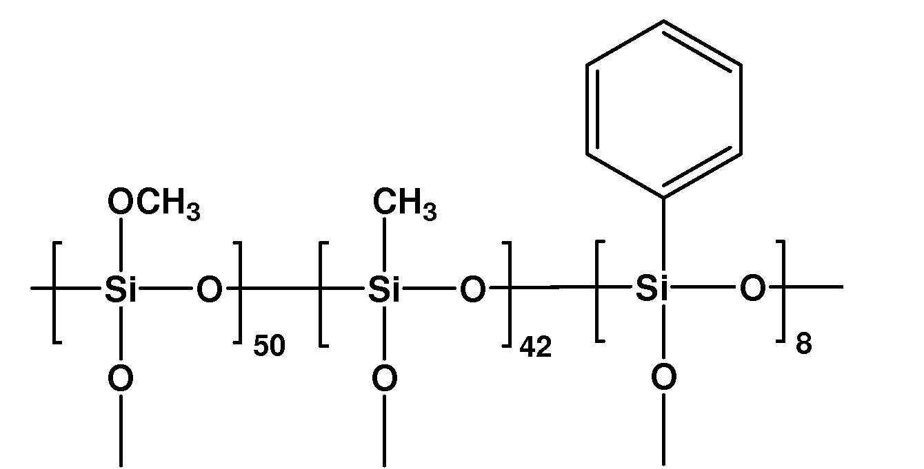
- organosiloxane (a) is a silicon compound represented by the following chemical formula.
- SF8421EG manufactured by Dow Corning Toray
- DPGM Dipropylene glycol monomethyl ether
- the non-dopant metal component (C) contained in the diffusing agent compositions of Example 1 and Comparative Examples 1 to 3 was measured using an atomic absorption spectrophotometer (Hitachi, Ltd., Z-2000). Table 2 shows the measurement results for the content of the non-dopant metal component (C). In addition, the measurement limit of the measurement by an atomic absorption spectrophotometer (Hitachi, Ltd. Z-2000) is 20 ppb. In Table 2, the inequality sign “ ⁇ ” indicates that the detection amount is less than the detection limit. In Example 1 and Comparative Examples 1 to 3, dibutyl phosphate is used as the dopant component (B). The content of Na is adjusted by adjusting the degree of purification of dibutyl phosphate.
- Example 1 and Comparative Examples 1 to 3 coating was performed on a P-type Si substrate (plane orientation ⁇ 100>, resistivity 5 to 15 ⁇ ⁇ cm) by a spin coating method.
- the film thickness of the diffusing agent composition applied on the Si substrate is about 7000 mm.
- heating was performed at 950 ° C. for 30 minutes in a nitrogen atmosphere using a heating furnace (VF-1000 manufactured by Koyo Thermo System).
- VF-1000 manufactured by Koyo Thermo System
- the Si substrate was immersed in a 5% HF aqueous solution for 10 minutes to remove the oxide film on the substrate surface. Note that two samples were prepared for each of Example 1 and Comparative Examples 1 to 3.
- the content of Na contained as the non-dopant metal component (C) is higher than that of Comparative Examples 1 to 3 where the content of Na contained as the non-dopant metal component (C) is 60 to 1000 ppb.
- Example 1 of less than 60 ppb it was confirmed that the sheet resistance value rapidly decreased. Since any element other than Na is below the detection limit, it is considered that the Na content greatly contributes to the improvement of the sheet resistance value.
- the present invention is applicable to fields related to a diffusing agent composition and an impurity diffusion layer.
Landscapes
- Photovoltaic Devices (AREA)
- Electroluminescent Light Sources (AREA)
- Engineering & Computer Science (AREA)
- Manufacturing & Machinery (AREA)
Abstract
Description
ケイ素化合物(A)は、SiO2微粒子、および下記一般式(1)で表されるアルコキシシランを加水分解して得られる反応生成物(以下、適宜、アルコキシシランの加水分解生成物という)からなる群から選ばれる少なくとも1種である。以下、SiO2微粒子、およびアルコキシシランの加水分解生成物のそれぞれについて説明する。

(II)式中、R51、R52、R53およびR54は、それぞれ独立に上記R2と同じアルキル基またはフェニル基などのアリール基を表す。a、b、cおよびdは、0≦a≦4、0≦b≦4、0≦c≦4、0≦d≦4であって、かつa+b+c+d=4の条件を満たす整数である。
(III)式中、R65は上記Rと同じ水素原子、アルキル基、またはフェニル基などのアリール基を表す。R66、R67、およびR68は、それぞれ独立に上記R2と同じアルキル基またはフェニル基などのアリール基を表す。e、f、およびgは、0≦e≦3、0≦f≦3、0≦g≦3であって、かつe+f+g=3の条件を満たす整数である。
(IV)式中、R70およびR71は上記R1と同じ水素原子、アルキル基、またはフェニル基などのアリール基を表す。ただし、R70およびR71のうちの少なくとも1つはアルキル基またはフェニル基などのアリール基を表す。R72、およびR73は、それぞれ独立に上記R2と同じアルキル基またはフェニル基などのアリール基を表す。hおよびiは、0≦h≦2、0≦i≦2であって、かつh+i=2の条件を満たす整数である。
[上記式(5)中、R13は、置換基を有していてもよい炭化水素基であり、Xはスルホン酸基である。]
SiO2微粒子の大きさは、平均粒径が1μm以下であることが好ましい。SiO2微粒子の具体例としては、ヒュームドシリカなどが挙げられる。
ドーパント成分(B)は、一般にドーパントとして用いられる化合物である。ドーパント成分(B)は、III族(13族)またはV族(15族)元素の化合物を含むN型またはP型のドーパント成分であり、半導体基板内にN型またはP型の不純物拡散層(不純物拡散領域)を形成することができる。ドーパント成分(B)に含まれるV族元素の化合物としては、たとえば、P2O5、リン酸ジブチル、リン酸トリブチル、リン酸モノエチル、リン酸ジエチル、リン酸トリエチル、リン酸モノプロピル、リン酸ジプロピルなどのリン酸エステル、Bi2O3、Sb(OCH2CH3)3、SbCl3、H3AsO4、As(OC4H9)3等が挙げられる。ドーパント成分(B)の濃度は、半導体基板に形成される不純物拡散層の層厚等に応じて適宜調整される。なお、III族のドーパント成分(B)としては、B2O3、Al2O3、三塩化ガリウム等が挙げられる。
非ドーパント金属成分(C)は、拡散剤組成物中に不純物(コンタミネーション)として含まれる不要な金属成分、たとえば、ケイ素化合物(A)等の原材料に含まれていて、精製工程で除去しきれずに残存した金属成分である。非ドーパント金属成分(C)として、たとえば、Na、Ca、Cu、Ni、Crなどが挙げられる。これらの非ドーパント金属成分(C)のうち、Naの含有量は組成物全体に対して60ppb未満であり、好ましくは20ppb未満である。
図1(A)~図1(D)、および図2(A)~図2(D)を参照して、N型の半導体基板にN型のドーパント成分(B)を含有する上述の拡散剤組成物を塗布または印刷してパターンを形成する工程と、拡散剤組成物中のドーパント成分(B)を半導体基板に拡散させる工程と、を含む不純物拡散層の形成方法と、これにより不純物拡散層が形成された半導体基板を備えた太陽電池の製造方法について説明する。図1(A)~図1(D)、および図2(A)~図2(D)は、実施形態に係る不純物拡散層の形成方法を含む太陽電池の製造方法を説明するための工程断面図である。
任意の回転塗布装置を用いて、拡散剤組成物2を半導体基板1の表面に回転塗布する。このようにして不純物拡散剤層を形成した後、オーブンなどの周知の手段を用いて塗布した拡散剤組成物2を乾燥させる。
実施例1~3および比較例1の拡散剤組成物の各成分および含有量を表1に示す。

DPGM:ジプロピレングリコールモノメチルエーテル
実施例、比較例の各拡散剤組成物について、その拡散性能の評価を実施した。なお、拡散性能は、シート抵抗値を測定することにより評価した。一般に、シート抵抗値が小さい程、拡散能力が高いとみなされる。シート抵抗値の評価の具体的な手法を以下に示す。

Claims (8)
- 半導体基板へのドーパント成分の拡散に用いられる拡散剤組成物であって、
ケイ素化合物(A)と、
ドーパント成分(B)と、
非ドーパント金属成分(C)と、
を含有し、
前記非ドーパント金属成分(C)として含まれるNaの含有量が組成物全体に対して60ppb未満であることを特徴とする拡散剤組成物。 - 前記ドーパント成分(B)は、III族元素またはV族元素の化合物を含む請求項1に記載の拡散剤組成物。
- 前記ケイ素化合物(A)は、SiO2微粒子、および下記一般式(1)で表されるアルコキシシランを加水分解して得られる反応生成物からなる群から選ばれる少なくとも1種である請求項1または2に記載の拡散剤組成物。

- 界面活性剤(D)をさらに含む請求項1に記載の拡散剤組成物。
- 溶剤成分(E)をさらに含む請求項1に記載の拡散剤組成物。
- 半導体基板に、請求項1に記載の拡散剤組成物を塗布して拡散層を形成する工程と、
前記拡散剤組成物のドーパント成分(B)を前記半導体基板に拡散させる拡散工程と、
を含むことを特徴とする不純物拡散層の形成方法。 - 前記拡散層の形成工程が、拡散剤組成物を印刷してパターンを形成するパターン形成工程を含む請求項6に記載の不純物拡散層の形成方法。
- 前記半導体基板が太陽電池に用いられる請求項6または7に記載の不純物拡散層の形成方法。
Priority Applications (3)
| Application Number | Priority Date | Filing Date | Title |
|---|---|---|---|
| KR1020137003310A KR20130086209A (ko) | 2010-07-09 | 2011-07-06 | 확산제 조성물 및 불순물 확산층의 형성 방법 |
| US13/808,371 US20130109123A1 (en) | 2010-07-09 | 2011-07-06 | Diffusing agent composition and method of forming impurity diffusion layer |
| CN201180033476.XA CN102986004B (zh) | 2010-07-09 | 2011-07-06 | 扩散剂组合物及杂质扩散层的形成方法 |
Applications Claiming Priority (2)
| Application Number | Priority Date | Filing Date | Title |
|---|---|---|---|
| JP2010157167A JP5681402B2 (ja) | 2010-07-09 | 2010-07-09 | 拡散剤組成物および不純物拡散層の形成方法 |
| JP2010-157167 | 2010-07-09 |
Publications (1)
| Publication Number | Publication Date |
|---|---|
| WO2012004996A1 true WO2012004996A1 (ja) | 2012-01-12 |
Family
ID=45440985
Family Applications (1)
| Application Number | Title | Priority Date | Filing Date |
|---|---|---|---|
| PCT/JP2011/003880 Ceased WO2012004996A1 (ja) | 2010-07-09 | 2011-07-06 | 拡散剤組成物および不純物拡散層の形成方法 |
Country Status (6)
| Country | Link |
|---|---|
| US (1) | US20130109123A1 (ja) |
| JP (1) | JP5681402B2 (ja) |
| KR (1) | KR20130086209A (ja) |
| CN (1) | CN102986004B (ja) |
| TW (1) | TWI485751B (ja) |
| WO (1) | WO2012004996A1 (ja) |
Cited By (1)
| Publication number | Priority date | Publication date | Assignee | Title |
|---|---|---|---|---|
| JP2013153052A (ja) * | 2012-01-25 | 2013-08-08 | Naoetsu Electronics Co Ltd | P型拡散層用塗布液 |
Families Citing this family (10)
| Publication number | Priority date | Publication date | Assignee | Title |
|---|---|---|---|---|
| TW201335278A (zh) * | 2012-02-23 | 2013-09-01 | 日立化成股份有限公司 | 不純物擴散層形成組成物、帶有不純物擴散層的半導體基板的製造方法以及太陽電池元件的製造方法 |
| JP6044397B2 (ja) * | 2012-03-07 | 2016-12-14 | 東レ株式会社 | マスクペースト組成物、これを用いて得られる半導体素子および半導体素子の製造方法 |
| EP2833391A4 (en) | 2012-03-30 | 2015-04-22 | Teijin Ltd | SEMICONDUCTOR LAMINATE AND METHOD FOR THE PRODUCTION THEREOF, METHOD FOR THE PRODUCTION OF A SEMICONDUCTOR COMPONENT, SEMICONDUCTOR ELEMENT, DOTING COMPOSITION, DOPING INJECTION LAYER AND METHOD FOR FORMING A DOPED LAYER |
| JP6139155B2 (ja) * | 2012-05-07 | 2017-05-31 | 東京応化工業株式会社 | 拡散剤組成物および不純物拡散層の形成方法 |
| JP6077907B2 (ja) * | 2013-03-29 | 2017-02-08 | 東京応化工業株式会社 | 拡散剤組成物および不純物拡散層の形成方法 |
| CN105408986B (zh) * | 2013-08-02 | 2018-05-22 | 东丽株式会社 | 掩模糊料组合物、使用其得到的半导体元件及半导体元件的制造方法 |
| JP6279878B2 (ja) * | 2013-10-31 | 2018-02-14 | 東京応化工業株式会社 | 太陽電池の製造方法 |
| JP6306855B2 (ja) * | 2013-10-31 | 2018-04-04 | 東京応化工業株式会社 | 太陽電池の製造方法 |
| JP2015225901A (ja) * | 2014-05-26 | 2015-12-14 | 東京応化工業株式会社 | 拡散剤組成物及び不純物拡散層の形成方法 |
| DE112015003040T5 (de) * | 2014-06-27 | 2017-03-23 | Keyence Corporation | Fotoelektrisches Multi-Wellenlängen-Messgerät, konfokales Messgerät, Interferenz-Messgerät und Farbmessgerät |
Citations (3)
| Publication number | Priority date | Publication date | Assignee | Title |
|---|---|---|---|---|
| JPH02229426A (ja) * | 1989-03-02 | 1990-09-12 | Toshiba Ceramics Co Ltd | ドーパントフィルム |
| JP2009501436A (ja) * | 2005-07-12 | 2009-01-15 | メルク パテント ゲゼルシャフト ミット ベシュレンクテル ハフトング | 二酸化シリコンおよび基礎のシリコンのためのエッチングとドーピング用の複合媒体 |
| JP2009253145A (ja) * | 2008-04-09 | 2009-10-29 | Tokyo Ohka Kogyo Co Ltd | 拡散層形成時の前処理方法 |
Family Cites Families (7)
| Publication number | Priority date | Publication date | Assignee | Title |
|---|---|---|---|---|
| CN101042950B (zh) * | 2003-12-12 | 2010-07-28 | 日本曹达株式会社 | 透明导电膜附着基体的制造方法 |
| JP4328303B2 (ja) * | 2004-09-16 | 2009-09-09 | 株式会社サンリック | 太陽光発電用多結晶シリコン原料および太陽光発電用シリコンウェーハ |
| CN101125645A (zh) * | 2007-07-30 | 2008-02-20 | 贵阳精一科技有限公司 | 一种电子级三氯氧磷的生产方法 |
| US20090056797A1 (en) * | 2007-08-28 | 2009-03-05 | Blue Square Energy Incorporated | Photovoltaic Thin-Film Solar Cell and Method Of Making The Same |
| JP5357442B2 (ja) * | 2008-04-09 | 2013-12-04 | 東京応化工業株式会社 | インクジェット用拡散剤組成物、当該組成物を用いた電極及び太陽電池の製造方法 |
| CA2739052A1 (en) * | 2008-09-30 | 2010-04-08 | Evonik Degussa Gmbh | Production of solar-grade silicon from silicon dioxide |
| US8324089B2 (en) * | 2009-07-23 | 2012-12-04 | Honeywell International Inc. | Compositions for forming doped regions in semiconductor substrates, methods for fabricating such compositions, and methods for forming doped regions using such compositions |
-
2010
- 2010-07-09 JP JP2010157167A patent/JP5681402B2/ja active Active
-
2011
- 2011-07-06 WO PCT/JP2011/003880 patent/WO2012004996A1/ja not_active Ceased
- 2011-07-06 US US13/808,371 patent/US20130109123A1/en not_active Abandoned
- 2011-07-06 CN CN201180033476.XA patent/CN102986004B/zh active Active
- 2011-07-06 KR KR1020137003310A patent/KR20130086209A/ko not_active Ceased
- 2011-07-08 TW TW100124209A patent/TWI485751B/zh active
Patent Citations (3)
| Publication number | Priority date | Publication date | Assignee | Title |
|---|---|---|---|---|
| JPH02229426A (ja) * | 1989-03-02 | 1990-09-12 | Toshiba Ceramics Co Ltd | ドーパントフィルム |
| JP2009501436A (ja) * | 2005-07-12 | 2009-01-15 | メルク パテント ゲゼルシャフト ミット ベシュレンクテル ハフトング | 二酸化シリコンおよび基礎のシリコンのためのエッチングとドーピング用の複合媒体 |
| JP2009253145A (ja) * | 2008-04-09 | 2009-10-29 | Tokyo Ohka Kogyo Co Ltd | 拡散層形成時の前処理方法 |
Cited By (1)
| Publication number | Priority date | Publication date | Assignee | Title |
|---|---|---|---|---|
| JP2013153052A (ja) * | 2012-01-25 | 2013-08-08 | Naoetsu Electronics Co Ltd | P型拡散層用塗布液 |
Also Published As
| Publication number | Publication date |
|---|---|
| CN102986004B (zh) | 2016-01-06 |
| JP5681402B2 (ja) | 2015-03-11 |
| KR20130086209A (ko) | 2013-07-31 |
| JP2012019162A (ja) | 2012-01-26 |
| US20130109123A1 (en) | 2013-05-02 |
| CN102986004A (zh) | 2013-03-20 |
| TWI485751B (zh) | 2015-05-21 |
| TW201218252A (en) | 2012-05-01 |
Similar Documents
| Publication | Publication Date | Title |
|---|---|---|
| JP5681402B2 (ja) | 拡散剤組成物および不純物拡散層の形成方法 | |
| JP5357442B2 (ja) | インクジェット用拡散剤組成物、当該組成物を用いた電極及び太陽電池の製造方法 | |
| JP5666267B2 (ja) | 塗布型拡散剤組成物 | |
| JP5555469B2 (ja) | 拡散剤組成物、および不純物拡散層の形成方法 | |
| KR101794374B1 (ko) | 확산제 조성물, 불순물 확산층의 형성 방법, 및 태양 전지 | |
| JP6022243B2 (ja) | 拡散剤組成物および不純物拡散層の形成方法 | |
| CN103374296B (zh) | 膜形成用组合物及其制造方法、扩散剂组合物及其制造方法 | |
| JP6310649B2 (ja) | 不純物拡散成分の拡散方法、及び太陽電池の製造方法 | |
| KR102225181B1 (ko) | 폴리실록산, 반도체용 재료, 반도체 및 태양 전지 제조 방법 | |
| JP6108781B2 (ja) | 不純物拡散成分の拡散方法、及び太陽電池の製造方法 |
Legal Events
| Date | Code | Title | Description |
|---|---|---|---|
| WWE | Wipo information: entry into national phase |
Ref document number: 201180033476.X Country of ref document: CN |
|
| 121 | Ep: the epo has been informed by wipo that ep was designated in this application |
Ref document number: 11803333 Country of ref document: EP Kind code of ref document: A1 |
|
| WWE | Wipo information: entry into national phase |
Ref document number: 13808371 Country of ref document: US |
|
| NENP | Non-entry into the national phase |
Ref country code: DE |
|
| ENP | Entry into the national phase |
Ref document number: 20137003310 Country of ref document: KR Kind code of ref document: A |
|
| 122 | Ep: pct application non-entry in european phase |
Ref document number: 11803333 Country of ref document: EP Kind code of ref document: A1 |