WO2012002282A1 - 成膜方法及び処理システム - Google Patents
成膜方法及び処理システム Download PDFInfo
- Publication number
- WO2012002282A1 WO2012002282A1 PCT/JP2011/064572 JP2011064572W WO2012002282A1 WO 2012002282 A1 WO2012002282 A1 WO 2012002282A1 JP 2011064572 W JP2011064572 W JP 2011064572W WO 2012002282 A1 WO2012002282 A1 WO 2012002282A1
- Authority
- WO
- WIPO (PCT)
- Prior art keywords
- film
- metal
- thin film
- film forming
- forming
- Prior art date
- Legal status (The legal status is an assumption and is not a legal conclusion. Google has not performed a legal analysis and makes no representation as to the accuracy of the status listed.)
- Ceased
Links
Images



Classifications
-
- B—PERFORMING OPERATIONS; TRANSPORTING
- B05—SPRAYING OR ATOMISING IN GENERAL; APPLYING FLUENT MATERIALS TO SURFACES, IN GENERAL
- B05D—PROCESSES FOR APPLYING FLUENT MATERIALS TO SURFACES, IN GENERAL
- B05D5/00—Processes for applying liquids or other fluent materials to surfaces to obtain special surface effects, finishes or structures
- B05D5/12—Processes for applying liquids or other fluent materials to surfaces to obtain special surface effects, finishes or structures to obtain a coating with specific electrical properties
-
- H—ELECTRICITY
- H10—SEMICONDUCTOR DEVICES; ELECTRIC SOLID-STATE DEVICES NOT OTHERWISE PROVIDED FOR
- H10W—GENERIC PACKAGES, INTERCONNECTIONS, CONNECTORS OR OTHER CONSTRUCTIONAL DETAILS OF DEVICES COVERED BY CLASS H10
- H10W20/00—Interconnections in chips, wafers or substrates
- H10W20/01—Manufacture or treatment
- H10W20/031—Manufacture or treatment of conductive parts of the interconnections
- H10W20/032—Manufacture or treatment of conductive parts of the interconnections of conductive barrier, adhesion or liner layers
- H10W20/042—Manufacture or treatment of conductive parts of the interconnections of conductive barrier, adhesion or liner layers the barrier, adhesion or liner layers being seed or nucleation layers
- H10W20/045—Manufacture or treatment of conductive parts of the interconnections of conductive barrier, adhesion or liner layers the barrier, adhesion or liner layers being seed or nucleation layers for deposition from the gaseous phase, e.g. for chemical vapour deposition [CVD]
-
- C—CHEMISTRY; METALLURGY
- C23—COATING METALLIC MATERIAL; COATING MATERIAL WITH METALLIC MATERIAL; CHEMICAL SURFACE TREATMENT; DIFFUSION TREATMENT OF METALLIC MATERIAL; COATING BY VACUUM EVAPORATION, BY SPUTTERING, BY ION IMPLANTATION OR BY CHEMICAL VAPOUR DEPOSITION, IN GENERAL; INHIBITING CORROSION OF METALLIC MATERIAL OR INCRUSTATION IN GENERAL
- C23C—COATING METALLIC MATERIAL; COATING MATERIAL WITH METALLIC MATERIAL; SURFACE TREATMENT OF METALLIC MATERIAL BY DIFFUSION INTO THE SURFACE, BY CHEMICAL CONVERSION OR SUBSTITUTION; COATING BY VACUUM EVAPORATION, BY SPUTTERING, BY ION IMPLANTATION OR BY CHEMICAL VAPOUR DEPOSITION, IN GENERAL
- C23C14/00—Coating by vacuum evaporation, by sputtering or by ion implantation of the coating forming material
- C23C14/04—Coating on selected surface areas, e.g. using masks
- C23C14/046—Coating cavities or hollow spaces, e.g. interior of tubes; Infiltration of porous substrates
-
- C—CHEMISTRY; METALLURGY
- C23—COATING METALLIC MATERIAL; COATING MATERIAL WITH METALLIC MATERIAL; CHEMICAL SURFACE TREATMENT; DIFFUSION TREATMENT OF METALLIC MATERIAL; COATING BY VACUUM EVAPORATION, BY SPUTTERING, BY ION IMPLANTATION OR BY CHEMICAL VAPOUR DEPOSITION, IN GENERAL; INHIBITING CORROSION OF METALLIC MATERIAL OR INCRUSTATION IN GENERAL
- C23C—COATING METALLIC MATERIAL; COATING MATERIAL WITH METALLIC MATERIAL; SURFACE TREATMENT OF METALLIC MATERIAL BY DIFFUSION INTO THE SURFACE, BY CHEMICAL CONVERSION OR SUBSTITUTION; COATING BY VACUUM EVAPORATION, BY SPUTTERING, BY ION IMPLANTATION OR BY CHEMICAL VAPOUR DEPOSITION, IN GENERAL
- C23C16/00—Chemical coating by decomposition of gaseous compounds, without leaving reaction products of surface material in the coating, i.e. chemical vapour deposition [CVD] processes
- C23C16/22—Chemical coating by decomposition of gaseous compounds, without leaving reaction products of surface material in the coating, i.e. chemical vapour deposition [CVD] processes characterised by the deposition of inorganic material, other than metallic material
- C23C16/30—Deposition of compounds, mixtures or solid solutions, e.g. borides, carbides, nitrides
- C23C16/40—Oxides
-
- H—ELECTRICITY
- H10—SEMICONDUCTOR DEVICES; ELECTRIC SOLID-STATE DEVICES NOT OTHERWISE PROVIDED FOR
- H10P—GENERIC PROCESSES OR APPARATUS FOR THE MANUFACTURE OR TREATMENT OF DEVICES COVERED BY CLASS H10
- H10P14/00—Formation of materials, e.g. in the shape of layers or pillars
- H10P14/20—Formation of materials, e.g. in the shape of layers or pillars of semiconductor materials
- H10P14/34—Deposited materials, e.g. layers
- H10P14/3402—Deposited materials, e.g. layers characterised by the chemical composition
- H10P14/3424—Deposited materials, e.g. layers characterised by the chemical composition being Group IIB-VIA materials
- H10P14/3426—Oxides
-
- H—ELECTRICITY
- H10—SEMICONDUCTOR DEVICES; ELECTRIC SOLID-STATE DEVICES NOT OTHERWISE PROVIDED FOR
- H10P—GENERIC PROCESSES OR APPARATUS FOR THE MANUFACTURE OR TREATMENT OF DEVICES COVERED BY CLASS H10
- H10P14/00—Formation of materials, e.g. in the shape of layers or pillars
- H10P14/60—Formation of materials, e.g. in the shape of layers or pillars of insulating materials
- H10P14/63—Formation of materials, e.g. in the shape of layers or pillars of insulating materials characterised by the formation processes
- H10P14/6302—Non-deposition formation processes
- H10P14/6304—Formation by oxidation, e.g. oxidation of the substrate
-
- H—ELECTRICITY
- H10—SEMICONDUCTOR DEVICES; ELECTRIC SOLID-STATE DEVICES NOT OTHERWISE PROVIDED FOR
- H10W—GENERIC PACKAGES, INTERCONNECTIONS, CONNECTORS OR OTHER CONSTRUCTIONAL DETAILS OF DEVICES COVERED BY CLASS H10
- H10W20/00—Interconnections in chips, wafers or substrates
- H10W20/01—Manufacture or treatment
- H10W20/031—Manufacture or treatment of conductive parts of the interconnections
- H10W20/032—Manufacture or treatment of conductive parts of the interconnections of conductive barrier, adhesion or liner layers
- H10W20/033—Manufacture or treatment of conductive parts of the interconnections of conductive barrier, adhesion or liner layers in openings in dielectrics
- H10W20/035—Manufacture or treatment of conductive parts of the interconnections of conductive barrier, adhesion or liner layers in openings in dielectrics combinations of barrier, adhesion or liner layers, e.g. multi-layered barrier layers
-
- H—ELECTRICITY
- H10—SEMICONDUCTOR DEVICES; ELECTRIC SOLID-STATE DEVICES NOT OTHERWISE PROVIDED FOR
- H10W—GENERIC PACKAGES, INTERCONNECTIONS, CONNECTORS OR OTHER CONSTRUCTIONAL DETAILS OF DEVICES COVERED BY CLASS H10
- H10W20/00—Interconnections in chips, wafers or substrates
- H10W20/01—Manufacture or treatment
- H10W20/031—Manufacture or treatment of conductive parts of the interconnections
- H10W20/032—Manufacture or treatment of conductive parts of the interconnections of conductive barrier, adhesion or liner layers
- H10W20/042—Manufacture or treatment of conductive parts of the interconnections of conductive barrier, adhesion or liner layers the barrier, adhesion or liner layers being seed or nucleation layers
- H10W20/043—Manufacture or treatment of conductive parts of the interconnections of conductive barrier, adhesion or liner layers the barrier, adhesion or liner layers being seed or nucleation layers for electroplating
-
- H—ELECTRICITY
- H10—SEMICONDUCTOR DEVICES; ELECTRIC SOLID-STATE DEVICES NOT OTHERWISE PROVIDED FOR
- H10W—GENERIC PACKAGES, INTERCONNECTIONS, CONNECTORS OR OTHER CONSTRUCTIONAL DETAILS OF DEVICES COVERED BY CLASS H10
- H10W20/00—Interconnections in chips, wafers or substrates
- H10W20/01—Manufacture or treatment
- H10W20/031—Manufacture or treatment of conductive parts of the interconnections
- H10W20/032—Manufacture or treatment of conductive parts of the interconnections of conductive barrier, adhesion or liner layers
- H10W20/047—Manufacture or treatment of conductive parts of the interconnections of conductive barrier, adhesion or liner layers by introducing additional elements therein
- H10W20/048—Manufacture or treatment of conductive parts of the interconnections of conductive barrier, adhesion or liner layers by introducing additional elements therein by using plasmas or gaseous environments, e.g. by nitriding
-
- H—ELECTRICITY
- H10—SEMICONDUCTOR DEVICES; ELECTRIC SOLID-STATE DEVICES NOT OTHERWISE PROVIDED FOR
- H10W—GENERIC PACKAGES, INTERCONNECTIONS, CONNECTORS OR OTHER CONSTRUCTIONAL DETAILS OF DEVICES COVERED BY CLASS H10
- H10W20/00—Interconnections in chips, wafers or substrates
- H10W20/01—Manufacture or treatment
- H10W20/031—Manufacture or treatment of conductive parts of the interconnections
- H10W20/032—Manufacture or treatment of conductive parts of the interconnections of conductive barrier, adhesion or liner layers
- H10W20/052—Manufacture or treatment of conductive parts of the interconnections of conductive barrier, adhesion or liner layers by treatments not introducing additional elements therein
-
- H—ELECTRICITY
- H10—SEMICONDUCTOR DEVICES; ELECTRIC SOLID-STATE DEVICES NOT OTHERWISE PROVIDED FOR
- H10W—GENERIC PACKAGES, INTERCONNECTIONS, CONNECTORS OR OTHER CONSTRUCTIONAL DETAILS OF DEVICES COVERED BY CLASS H10
- H10W20/00—Interconnections in chips, wafers or substrates
- H10W20/01—Manufacture or treatment
- H10W20/031—Manufacture or treatment of conductive parts of the interconnections
- H10W20/032—Manufacture or treatment of conductive parts of the interconnections of conductive barrier, adhesion or liner layers
- H10W20/055—Manufacture or treatment of conductive parts of the interconnections of conductive barrier, adhesion or liner layers by formation methods other than physical vapour deposition [PVD], chemical vapour deposition [CVD] or liquid deposition
-
- H—ELECTRICITY
- H10—SEMICONDUCTOR DEVICES; ELECTRIC SOLID-STATE DEVICES NOT OTHERWISE PROVIDED FOR
- H10W—GENERIC PACKAGES, INTERCONNECTIONS, CONNECTORS OR OTHER CONSTRUCTIONAL DETAILS OF DEVICES COVERED BY CLASS H10
- H10W20/00—Interconnections in chips, wafers or substrates
- H10W20/01—Manufacture or treatment
- H10W20/031—Manufacture or treatment of conductive parts of the interconnections
- H10W20/032—Manufacture or treatment of conductive parts of the interconnections of conductive barrier, adhesion or liner layers
- H10W20/055—Manufacture or treatment of conductive parts of the interconnections of conductive barrier, adhesion or liner layers by formation methods other than physical vapour deposition [PVD], chemical vapour deposition [CVD] or liquid deposition
- H10W20/0552—Manufacture or treatment of conductive parts of the interconnections of conductive barrier, adhesion or liner layers by formation methods other than physical vapour deposition [PVD], chemical vapour deposition [CVD] or liquid deposition by diffusing metallic dopants to react with dielectrics
-
- H—ELECTRICITY
- H10—SEMICONDUCTOR DEVICES; ELECTRIC SOLID-STATE DEVICES NOT OTHERWISE PROVIDED FOR
- H10W—GENERIC PACKAGES, INTERCONNECTIONS, CONNECTORS OR OTHER CONSTRUCTIONAL DETAILS OF DEVICES COVERED BY CLASS H10
- H10W20/00—Interconnections in chips, wafers or substrates
- H10W20/01—Manufacture or treatment
- H10W20/071—Manufacture or treatment of dielectric parts thereof
- H10W20/074—Manufacture or treatment of dielectric parts thereof of dielectric parts comprising thin functional dielectric layers, e.g. dielectric etch-stop, barrier, capping or liner layers
- H10W20/076—Manufacture or treatment of dielectric parts thereof of dielectric parts comprising thin functional dielectric layers, e.g. dielectric etch-stop, barrier, capping or liner layers in via holes or trenches
-
- H—ELECTRICITY
- H10—SEMICONDUCTOR DEVICES; ELECTRIC SOLID-STATE DEVICES NOT OTHERWISE PROVIDED FOR
- H10W—GENERIC PACKAGES, INTERCONNECTIONS, CONNECTORS OR OTHER CONSTRUCTIONAL DETAILS OF DEVICES COVERED BY CLASS H10
- H10W20/00—Interconnections in chips, wafers or substrates
- H10W20/40—Interconnections external to wafers or substrates, e.g. back-end-of-line [BEOL] metallisations or vias connecting to gate electrodes
- H10W20/41—Interconnections external to wafers or substrates, e.g. back-end-of-line [BEOL] metallisations or vias connecting to gate electrodes characterised by their conductive parts
- H10W20/425—Barrier, adhesion or liner layers
-
- H—ELECTRICITY
- H10—SEMICONDUCTOR DEVICES; ELECTRIC SOLID-STATE DEVICES NOT OTHERWISE PROVIDED FOR
- H10W—GENERIC PACKAGES, INTERCONNECTIONS, CONNECTORS OR OTHER CONSTRUCTIONAL DETAILS OF DEVICES COVERED BY CLASS H10
- H10W20/00—Interconnections in chips, wafers or substrates
- H10W20/40—Interconnections external to wafers or substrates, e.g. back-end-of-line [BEOL] metallisations or vias connecting to gate electrodes
- H10W20/45—Interconnections external to wafers or substrates, e.g. back-end-of-line [BEOL] metallisations or vias connecting to gate electrodes characterised by their insulating parts
- H10W20/48—Insulating materials thereof
Definitions
- the present invention relates to a film forming method and a processing system when wiring is performed by embedding a recess of an interlayer insulating film having a low relative dielectric constant formed on the surface of an object to be processed such as a semiconductor wafer with copper or the like.
- a semiconductor device is repeatedly subjected to various processes such as a film forming process and a pattern etching process to manufacture a desired device.
- the line width and hole diameter are becoming increasingly finer than requested.
- a wiring material or a material embedded in a recess such as a trench or a hole, there is a tendency to use copper which has a very low electric resistance and is inexpensive because it is necessary to reduce the electric resistance by miniaturizing various dimensions.
- tantalum metal Ti
- tantalum nitride film TiN
- a thin seed film made of a copper film is formed on the entire wafer surface including the entire wall surface in the recess, and then the copper is formed on the entire wafer surface.
- the inside of the recess is completely embedded.
- an excessive copper thin film on the wafer surface is removed by polishing by CMP (Chemical Chemical Mechanical) processing or the like.
- FIGS. 7A to 7C are views showing a conventional embedding process of a recess of a semiconductor wafer.
- the surface of the insulating layer 1 formed on the semiconductor wafer W such as an interlayer insulating film made of, for example, a SiO2 film, is formed with via holes, through holes, or trenches (trench) by a single-damascene structure, a dual-damascene structure, a three-dimensional mounting structure, or the like.
- a lower wiring layer 3 made of a metal film such as copper is exposed at the bottom of the recess 2.
- the recess 2 is composed of a groove (trench) 2A having an elongated cross section and a hole 2B formed in a part of the bottom of the groove 2A.
- the hole 2B is a via hole or a through hole. It becomes.
- the wiring layer 3 is exposed at the bottom of the hole 2B, and is electrically connected to a lower wiring layer and an element such as a transistor. Note that illustration of elements such as lower wiring layers and transistors is omitted.
- the recess 2 has a very small width or inner diameter of about 120 nm, for example, and an aspect ratio of about 2 to 4, for example. Note that the diffusion prevention film, the etching stop film, and the like are not shown and simplified in shape.
- a barrier layer 4 made of, for example, a TaN film and a stacked structure of Ta films is formed in advance on the surface of the semiconductor wafer W by a plasma sputtering apparatus, including the inner surface of the recess 2 (see FIG. 7A). )reference). Then, a seed film 6 made of a thin copper film is formed as a metal film over the entire wafer surface including the surface in the recess 2 by a plasma sputtering apparatus (see FIG. 7B). The recess 2 is filled with a metal film 8 made of, for example, a copper film by performing a copper plating process on the wafer surface (see FIG. 7C). Thereafter, the excess metal film 8, seed film 6 and barrier layer 4 on the wafer surface are removed by polishing using the above-described CMP process or the like.
- a self-formed barrier layer using a Mn film or a CuMn alloy film instead of the Ta film or TaN film has attracted attention.
- the Mn film or CuMn alloy film is formed by sputtering, and the Mn film or CuMn alloy film itself becomes a seed film. Therefore, a Cu plating layer can be directly formed thereon, and annealing can be performed after plating.
- MnSixOy (x, y: arbitrary positive number) film or a Mn and SiO2 layer is formed at the boundary between the SiO2 layer and the Mn film or CuMn alloy film. Since a barrier film called a manganese oxide MnOx (x: arbitrary positive number) film formed by reaction with oxygen is formed, there is an advantage that the number of manufacturing steps can be reduced. Manganese oxides are classified into MnO, Mn3O4, Mn2O3, MnO2 and the like depending on the valence of Mn. In this specification, these are collectively referred to as MnOx. This also applies to TaOx described later.
- TEOS is used as a material for the interlayer insulating film.
- a low-k film made of SiOC, SiCOH or the like containing an organic group such as a methyl group as a material having a lower relative dielectric constant has been studied.
- the relative dielectric constant of the silicon oxide film formed using the TEOS is about 4.1
- the relative dielectric constant of SiOC is about 3.0.
- the interlayer insulating film when a material with a low relative dielectric constant such as the Low-k film (SiOC) is used as the interlayer insulating film, CVD is performed on the surface of the interlayer insulating film with a low relative dielectric constant including the exposed surface in the recess. Even when the Mn-containing film is formed by the above method, the MnOx film is hardly deposited, so that there is a problem that the barrier layer cannot be formed.
- SiOC Low-k film
- An object of the present invention is to provide a film forming method and a processing system capable of efficiently forming a thin film containing a metal such as Mn, such as a MnOx film, on the surface of an insulating layer having a low relative dielectric constant.
- a film forming method for forming a first thin film made of a first metal in a film forming method for performing a film forming process on a target object having an insulating layer formed on a surface thereof A step, an oxidation step of oxidizing the first thin film to form an oxide film, and a second thin film formation step of forming a second thin film containing a second metal on the oxide film.
- a film forming method characterized by the following.
- a second thin film containing, for example, manganese (Mn) as a second metal, such as a manganese oxide (MnOx) film can be easily formed on the surface of an insulating layer made of a so-called Low-k film having a low relative dielectric constant. It becomes possible to form.
- Mn manganese
- MnOx manganese oxide
- the invention according to claim 2 is an oxide film forming step of forming an oxide film containing a first metal in a film forming method for performing a film forming process on a target object having an insulating layer formed on a surface thereof; And a second thin film forming step of forming a second thin film containing a second metal on the oxide film.
- a second thin film containing, for example, manganese (Mn) as a second metal, such as a manganese oxide (MnOx) film can be easily formed on the surface of an insulating layer made of a so-called Low-k film having a low relative dielectric constant. It becomes possible to form.
- Mn manganese
- MnOx manganese oxide
- a film forming method for forming a first thin film made of a first metal in a film forming method for performing a film forming process on an object having an insulating layer formed on a surface thereof A step of oxidizing the first thin film to form an oxide film; a third film forming step of forming a third film containing Cu on the oxide film; and And a second thin film forming step of supplying a source gas containing a second metal to form a second thin film at the interface between the oxide film and the third film. Is the method.
- a second thin film for example, a manganese oxide (MnOx) film
- the invention according to claim 5 is an oxide film forming step of forming an oxide film containing a first metal in a film forming method for performing a film forming process on an object to be processed on which an insulating layer is formed.
- a second thin film for example, a manganese oxide (MnOx) film
- a film forming method for forming a first thin film made of a first metal in a film forming method for performing a film forming process on a target object having an insulating layer formed on a surface thereof A step of forming a third film containing Cu on the first thin film; and a source gas containing a second metal on the third film to supply the oxide film
- a second thin film forming step of forming a second thin film at the interface between the first film and the third film is provided.
- a second thin film for example, a manganese oxide (MnOx) film
- the first thin film made of the first metal is formed on the surface of the target object.
- a processing apparatus that oxidizes the first thin film to form an oxide film a processing apparatus that forms a second thin film containing a second metal on the oxide film, and the processing apparatuses 2.
- a system control unit that controls the entire system.
- a process of forming an oxide film containing a first metal on the surface of the target object An apparatus, a processing apparatus for forming a second thin film containing a second metal on the oxide film, a common transfer chamber to which the respective processing apparatuses are connected, and each of the processes provided in the common transfer chamber.
- a processing system comprising: a transport mechanism for transporting the object to be processed into an apparatus; and a system control unit for controlling the entire processing system so as to perform the film forming method according to claim 2. It is.
- manganese (Mn) as the second metal is formed on the surface of the insulating layer made of a so-called Low-k film having a low relative dielectric constant, for example.
- a second thin film including, for example, a manganese oxide (MnOx) film can be easily formed.
- a second thin film for example, a manganese oxide (MnOx) film is self-formed at the boundary portion between the first thin film and the third film. Can be formed more easily.
- MnOx manganese oxide
- FIG. 1 is a schematic configuration diagram showing a processing system of the present invention
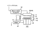
- FIG. 2 is a schematic configuration diagram showing an example of a processing apparatus.
- a case where Ta is used as the first metal and Mn is used as the second metal will be described as an example.
- the processing system 10 mainly has a plurality of, for example, four processing apparatuses 12A, 12B, 12C, and 12D, and a common transfer chamber 14 having a substantially hexagonal shape.
- the common transfer chamber 14 is further connected to first and second load lock chambers 16A and 16B having a load lock function, and an elongated introduction-side transfer chamber 18 is further connected thereto.
- the first processing apparatus for example, the processing apparatus 12A
- the third processing apparatus for example, the processing apparatus 12C is configured as a third processing apparatus 12C that forms a second thin film containing a second metal such as Mn on the semiconductor wafer W
- the fourth processing apparatus for example, the processing apparatus 12D is configured as a fourth processing apparatus 12D that deposits, for example, a copper film as a metal that is a material of the embedded metal on the semiconductor wafer W.
- the fourth processing apparatus 12D may not be provided here, and the processing in the fourth processing apparatus may be performed in another processing apparatus provided in addition to the processing system 10.
- the fourth processing apparatus 12D includes a CVD method, an ALD method, a PVD (sputtering) method, a supercritical CO2 method, an electroless plating method, an electrolytic plating method, a CVD-Cu seed + electrolytic plating method, and a sputtered Cu seed + electrolysis.
- a film forming apparatus such as a plating method is used.
- the processing apparatuses 12A to 12D are joined to four sides of the substantially hexagonal common transfer chamber 14, and the first and second load lock chambers 16A and 16B are joined to the other two sides. Each is joined.
- the introduction-side transfer chamber 18 is commonly connected to the first and second load lock chambers 16A and 16B.
- the common transfer chamber 14 and the four processing devices 12A to 12D and the common transfer chamber 14 and the first and second load lock chambers 16A and 16B can be opened and closed in an airtight manner.
- a gate valve G is joined to form a cluster tool, and can communicate with the common transfer chamber 14 as necessary.
- the common transfer chamber 14 is evacuated.
- gate valves G that can be opened and closed in an airtight manner are interposed.
- the first and second load lock chambers 16A and 16B are repeatedly evacuated and returned to atmospheric pressure as the wafer is carried in and out.
- a transfer mechanism comprising an articulated arm that can be bent and extended at a position accessible to the two load lock chambers 16A and 16B and the four processing devices 12A to 12D.
- 20 has two picks 20A and 20B that can be bent and stretched independently in opposite directions, for example, so that two wafers can be handled at a time.
- the introduction-side transfer chamber 18 is formed by a horizontally long box, and one or a plurality of, in the illustrated example, three carry-in portions for introducing a semiconductor wafer as an object to be processed are formed on one side of the horizontally long.
- An opening is provided, and an opening / closing door 22 that can be opened and closed is provided at each carry-in entrance.
- An introduction port 24 is provided in correspondence with each carry-in port, and one cassette container 26 can be placed on each of the introduction ports 24.
- a plurality of, for example, 25 wafers W can be placed and accommodated in multiple stages at an equal pitch.
- the cassette container 26 is sealed, for example, and filled with an atmosphere of an inert gas such as N 2 soot gas.
- an introduction-side transfer mechanism 28 for transferring the wafer W along its longitudinal direction is provided.
- the introduction-side transport mechanism 28 has two picks 28A and 28B that can be bent and stretched and swiveled, and can handle two wafers W at a time.
- This introduction side conveyance mechanism 28 is supported in the introduction side conveyance chamber 18 so as to be slidable on a guide rail 30 provided so as to extend along the length direction thereof.
- an orienter 32 for aligning the wafer is provided at one end of the introduction-side transfer chamber 18.
- the orienter 32 has a turntable 32A that is rotated by a drive motor, and rotates with the wafer W mounted thereon.
- An optical sensor 32B for detecting the peripheral edge of the wafer W is provided on the outer periphery of the turntable 32A, whereby the positioning notch of the wafer W, for example, the position direction of the notch or the orientation flat or the position of the center of the wafer W is provided. The amount of deviation can be detected.
- the third processing apparatus 12C has a processing container 40 that can be evacuated.
- the processing container 40 is set such that the upper space has a large diameter and the lower space has a small diameter.
- a mounting table 42 is provided upright from the bottom, and the semiconductor wafer W can be mounted on the upper surface thereof.
- a heating means 44 made of a resistance heater is provided to heat the wafer W.
- an exhaust system 46 is connected to the bottom side of the processing container 40 so that the atmosphere in the processing container 40 can be evacuated while controlling the pressure.
- the side wall of the processing container 40 is connected to the common transfer chamber 14 via the gate valve G.
- the processing container 40 is provided with a gas introduction means 48 for introducing a necessary gas.
- the gas introducing means 48 includes a shower head 50 provided on the container ceiling portion so as to face the mounting table 42, and can inject gas toward the processing space S below the shower head 50. ing.
- the shower head 50 is connected to a source gas supply system 52 for supplying a source gas necessary for the film forming process here, so that the source gas can be supplied while controlling the flow rate.
- an organic metal material containing Mn is used as a raw material, and specifically, (EtCp) 2 Mn is used.
- This raw material is heated to a temperature for obtaining a vapor pressure sufficient for supply, and is in a liquid state if the heating temperature exceeds the melting point, and is vaporized by being bubbled by a bubbling gas such as Ar, Supplied with this bubbling gas.
- the bubbling gas is not limited to Ar, and other rare gases such as He, or H 2 soot gas or N 2 soot gas can also be used.
- MnCp2 Mn (C5H5) 2
- the processing system 10 as described above has a system control unit 34 composed of, for example, a computer in order to control the operation of the entire system.
- a program necessary for controlling the operation of the entire processing system is stored in a storage medium 36 such as a flexible disk, a CD (Compact Disc), a hard disk, or a flash memory.
- a storage medium 36 such as a flexible disk, a CD (Compact Disc), a hard disk, or a flash memory.
- the start, stop and flow control of each gas control of process temperature (wafer temperature), process pressure (pressure in the processing container of each processing apparatus), A wafer transfer operation or the like is performed.
- FIGS. 3 (A) to 3 (E) are flowcharts showing the steps of the method of the present invention
- FIG. 3 (A) shows a first embodiment of the method of the present invention
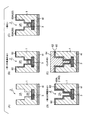
- 4 (A) to 4 (E) are diagrams showing an example of a thin film deposition state in each step of the first embodiment of the method of the present invention.
- an unprocessed semiconductor wafer W is taken into the introduction-side transfer chamber 18 from the cassette container 26 installed in the introduction port 24 by the introduction-side transfer mechanism 28, and the acquired wafer W is introduced into the introduction-side transfer chamber 18. Is transferred to an orienter 32 provided at one end of the head, and positioning is performed here.
- the surface of the insulating layer 1 such as an interlayer insulating film formed on the wafer W has a trench or a hole.
- a recess 2 is formed, and a lower wiring layer 3 made of copper or the like is exposed as a metal layer at the bottom of the recess 2.
- the recess 2 is composed of a groove (trench) 2A having an elongated cross section and a hole 2B formed in a part of the bottom of the groove 2A.
- the hole 2B becomes a contact hole or a through hole.
- the wiring layer 3 is exposed as a metal layer at the bottom of the hole 2B, and is electrically connected to a lower wiring layer and an element such as a transistor.
- the insulating layer 1 serving as a base film is made of a low-k film, for example, SiOC, which is a low dielectric constant material having a relative dielectric constant lower than 4.1.
- the wafer W that has been positioned as described above is transferred again by the introduction-side transfer mechanism 28 and carried into one of the first or second load lock chambers 16A and 16B. After the load lock chamber is evacuated, the wafer W in the load lock chamber is taken into the common transfer chamber 14 using the transfer mechanism 20 in the common transfer chamber 14 that has been evacuated in advance.
- an unprocessed wafer taken into the common transfer chamber 14 is first loaded into the first processing apparatus 12A, where Then, a first thin film forming step (S1) is performed on the wafer W to form a first thin film made of a Ta metal film by sputtering, for example.
- the wafer W on which the formation of the first thin film has been completed is then carried into the second processing apparatus 12B, where the first thin film formed on the surface of the wafer W is oxidized to form an oxide film, An oxidation step (S2) for forming TaOx is performed.
- the wafer W on which the formation of the oxide film has been completed is then carried into the third processing apparatus 12C, where a second metal containing a second metal having a barrier property against the embedded metal in the recess is formed on the surface of the wafer W.
- a second thin film forming step (S3) for forming the second thin film is performed.
- a MnOx film is formed as the second thin film.
- a barrier layer for the Cu film is formed with the layer structure of the first thin film and the second thin film.
- the wafer W on which the second thin film forming step has been completed is then carried into the fourth processing apparatus 12D, where, for example, a copper film is deposited on the surface of the wafer W as a buried metal, and the inside of the recess 2 is formed.
- An embedding process (S4) for embedding is performed as a third film forming process. And if the said embedding process is completed, the process in this processing system 10 will be completed.
- the processed wafer W is accommodated in the processed wafer cassette container 26 of the introduction port 24 via one of the load lock chambers 16A or 16B and the introduction-side transfer chamber 18. Note that the inside of the common transfer chamber 14 is decompressed in an atmosphere of a rare gas such as Ar or He or an inert gas such as dry N 2 soot.
- the first processing apparatus 12A is formed as a sputtering apparatus, and Ta metal is used as a metal target.
- the first thin film forming step S1 the first thin film 60 is very thinly formed on the surface of the wafer W as shown in FIG. 4A by sputtering as shown in FIG. 4B. Thereby, the 1st thin film 60 is formed in the whole surface including the whole inner surface of the recessed part 2.
- FIG. This first thin film 60 is made of a Ta metal film as described above. If this film thickness is too thick, the amount of copper embedded in the recesses 2 in the subsequent process is reduced, causing an increase in wiring resistance and contact resistance. In order to prevent this, the film thickness of the first thin film 60 is preferably set to 2 nm or less.
- the sputtering method is used to form the first thin film 60.
- the present invention is not limited to this, and the CVD method or ALD (Atomic Layer Deposition) in which the source gas and the reducing gas are alternately flowed repeatedly is used. ) Method can also be used.
- the second processing apparatus 12B is formed as an annealing apparatus, for example, and an oxidation process is performed.
- the oxidation step S2 the Ta metal film as the first thin film 60 is oxidized to form an oxide film 60A, that is, a TaOx film, as shown in FIG.
- the wafer W may be heated and oxidized while supplying a rare gas such as Ar gas or an inert gas such as N 2 soot gas without supplying the oxidizing gas, or the wafer W may be simply oxidized without supplying any gas. You may oxidize by heating and annealing. In this case, moisture and oxygen components contained in the underlying insulating layer 1 react with the Ta metal film to form TaOx as the oxide film 60A. In this case, the Ta metal film in contact with the lower wiring layer 3 made of copper or the like exposed at the bottom of the recess 2 in the state shown in FIG.
- a rare gas such as Ar gas or an inert gas such as N 2 soot gas
- the MnOx film is formed in the subsequent second thin film forming step because the Ta metal film in contact with the wiring layer 3 is formed. It becomes the part other than. That is, a laminated structure made of MnOx / Ta is formed on the upper surface of the insulating film 1 and on the side walls of the trench (trench) 2A and the hole 2B, while only Ta is formed at the bottom of the hole 2B. It can be expected that the wiring resistance (via resistance) is reduced.
- the wafer W is transferred to the outside of the processing system in the state shown in FIG. 4B, that is, in the state where the Ta metal film as the first thin film 60 is formed.
- the Ta metal film may be oxidized with an oxygen component or a water vapor component in the atmosphere.
- water may be physically adsorbed on the surface of the oxide film 60A containing the first metal formed through the above-described oxidation step S2.
- water may be separately supplied into the chamber, the moisture released from the insulating film 1 by heating, or the water vapor component in the atmosphere may be used.
- the third processing apparatus 12C is formed as shown in FIG.
- a second thin film 62 containing Mn as the second metal, that is, MnOx is formed on the oxide film 60A as shown in FIG. 4D.
- the wafer W mounted on the mounting table 42 is heated within a range of, for example, 100 to 400 ° C., for example, about 200 ° C., and the raw material gas supply system 52 uses bubbling gas.
- the raw material is vaporized to generate a raw material gas of Mn, and this raw material gas is supplied from the shower head 50 to the processing space S of the processing container 40.
- the process pressure is in the range of 100 to 105 Pa, for example, about 133 Pa
- the Mn source gas is about 0.1 to 10 sccm
- the carrier gas is about 10 to 500 sccm.
- the raw material gas accompanied with the bubbling gas is supplied into the processing container 40.
- Mn source gas or metal Mn is deposited on the TaOx film as the oxide film 60A by CVD, the Mn source gas or metal Mn is immediately adsorbed to the oxygen component of the underlying TaOx film or / and the physical adsorption of the surface.
- a MnOx film is formed as the second thin film 62 by reacting with water.
- the oxide film 60A is reduced, it returns to the Ta metal film 60 (first thin film).
- the surface of the insulating film 1 has a hydrophobic tendency, the adhesion probability of Mn source gas and water having a function of decomposing the Mn source gas is remarkably lowered. Formation tends to be inhibited.
- the TaOx film is first formed on the insulating film 1, the hydrophobicity of the substrate surface is covered with the TaOx film and tends to be hydrophilic, so that the Mn source gas adheres very much to the surface.
- the raw material gas adhering to the surface is decomposed or oxidized to temporarily deposit Mn of the metal film, but this metal Mn is immediately oxidized, resulting in MnOx. A film will be formed immediately.
- the TaOx film as the oxide film 60A is formed as a base, so that the MnOx film is very easily attached or deposited.
- a film can be formed.
- the metal Mn deposited on the surface of the wafer W by removing oxygen from the underlying oxide film, so that the first metal, for example, a metal oxide containing Cu (
- the first metal for example, a metal oxide containing Cu
- the second metal for example, a metal oxide containing Mn (MnOx).
- a barrier layer having a two-layer structure composed of the first thin film 60 and the second thin film 62 is formed.
- the metal Mn since the second metal deposited on the surface of the wafer W, for example, the metal Mn, needs to be oxidized by taking oxygen from the physical adsorption water on the surface of the underlying oxide film, Each metal is selected so that the standard free energy of formation of a metal oxide such as Mn-containing metal oxide (MnOx) is equal to or smaller than the standard free energy of formation of the physically adsorbed water (H 2 O). In this way, a barrier layer having a two-layer structure composed of the first thin film 60 and the second thin film 62 is formed.
- Mn-containing metal oxide Mn-containing metal oxide
- the embedding step S4 is performed as shown in FIG. Thereby, the embedded metal 64 is formed on the entire wafer surface at the same time as the recess 2 is completely embedded.
- Cu Cu film
- the embedded metal 64 may be formed by any of CVD, ALD, PVD (sputtering), supercritical CO 2 plating, electroless plating, and electrolytic plating.
- CVD chemical vapor deposition
- ALD atomic layer deposition
- PVD vapor deposition
- supercritical CO 2 plating electroless plating
- electrolytic plating electrolytic plating
- electrolytic plating method a Cu seed film is deposited by, for example, a sputtering method in the fourth processing apparatus 12D, and the processing apparatus provided outside the processing system 10 is applied. This embedding process may be performed.
- the film forming process is completed, and thereafter, the excess embedded metal 64 and the like on the wafer surface are removed by the CMP process.
- a second thin film containing, for example, manganese (Mn) as a second metal, such as a manganese oxide (MnOx) film can be easily formed on the surface of an insulating layer made of a so-called Low-k film having a low relative dielectric constant. Can be formed.
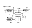
- FIG. 5 is a schematic configuration diagram showing a modification of the third processing apparatus as described above.
- the third processing apparatus 12C-1 is configured such that the oxidizing gas supply system 70 is simply connected to the shower head 50 with respect to the third processing apparatus 12C described above with reference to FIG. Has been. 5, the same components as those shown in FIG. 2 are denoted by the same reference numerals.
- O2 soot gas is supplied as an oxidizing gas from the oxidizing gas supply system 70 when the oxidizing process is performed in the processing apparatus 12C-1, and Mn source gas is supplied from the source gas supply system 52 when the second thin film forming process is performed.
- a second embodiment of the method of the present invention will be described.
- a first thin film forming step S1 for forming a Ta film and an oxidizing step S2 for oxidizing the Ta film to form a TaOx film
- the present invention is not limited to this, and a TaOx film is formed as an oxide film forming process in one step (S1-1) as in the second embodiment shown in FIG. 3B. You may do it.
- sputtering may be performed using a TaOx target as a target in the sputtering apparatus, and as described above, the TaOx film can be formed in one step.
- the device configuration can be greatly simplified.
- the embedding step S4 is performed after the second thin film forming step S3.
- the present invention is not limited to this.
- the embedding step S4 may be performed after the oxidation step S2, and then the second thin film forming step S3 may be performed.
- Mn diffuses in Cu, and the MnOx film can be self-formed at the Cu / Ta interface. That is, when the source gas is supplied onto the Cu film, which is the third film, this source gas decomposes on the Cu surface and the generated Mn element diffuses in the Cu and the MnOx film (first 2 thin film) can be formed.
- a fourth embodiment of the method of the present invention will be described.
- a first thin film forming step S1 for forming a Ta film and an oxidizing step S2 for oxidizing the Ta film to form a TaOx film
- the present invention is not limited to this, and a TaOx film is formed as an oxide film forming process in one step (S1-1) as in the fourth embodiment shown in FIG. 3D. You may do it.
- impurities such as carbon derived from CVD in the second thin film forming step S3 do not exist at the Cu / Ta interface, improvement in adhesion can be expected.
- Mn diffuses in Cu and a MnOx film is self-formed at the Cu / Ta interface, so that a reliable barrier layer is formed. However, until such a barrier layer is formed, the oxide film 60A becomes a temporary barrier layer, and Cu is prevented from diffusing to the insulating film 1 side.
- Mn diffuses in Cu, and Mn is Cu / When it reaches the Ta interface, it reacts with moisture around the Ta, and a MnOx film is formed at the Cu / Ta interface.
- an annealing step S5 (shown by a dotted line in FIG. 3) may be added after the embedding step S4.
- an annealing step S5 (indicated by a dotted line in FIG. 3) may be added after the second thin film forming step S3.
- the process temperature is, for example, 300 to 500 ° C.
- the annealing process is performed for 0.5 to 10 hours in an inert gas atmosphere such as Ar or N2.
- the SiOC film is used as the Low-k film for forming the insulating layer 1
- the insulating layer includes the SiOC film, the SiCOH film, and the SiCN film.
- One or more films selected from the group consisting of: a silica film, a methylsilsesquioxane film, a polyarylene film, a SiOF film, and a fluorocarbon film can be used.
- SiLK registered trademark
- the first metal may be Mg, Al, Ca, Ti, V, Cr. , Mn, Fe, Co, Ni, Cu, Zn, Ga, Ge, Sr, Zr, Nb, Mo, Ru, Rh, Pd, Ag, Cd, In, Sn, Sb, Ba, Hf, Ta, W, Os
- One or more metals selected from the group consisting of Ir, Pt, and Au can be used.
- Mn is used as the second metal
- the present invention is not limited thereto, and examples of the second metal include Mg, Al, Ca, Ti, V, and Cr. , Mn, Fe, Co, Ni, Cu, Zn, Ga, Ge, Sr, Zr, Nb, Mo, Ru, Rh, Pd, Ag, Cd, In, Sn, Sb, Ba, Hf, Ta, W, Os
- metals selected from the group consisting of Ir, Pt, and Au can be used.
- the standard free energy of formation of the metal oxide containing the first metal is greater than the standard free energy of formation of the metal oxide containing the second metal.
- second metals are selected.
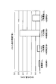
- FIG. 6 is a graph showing the evaluation results when the method of the present invention is carried out.
- two types of cases where Ta is used as the first metal and Cu is used are performed, and MnOx film is formed using Mn as the second metal.
- As oxidation treatment simple exposure to the atmosphere is performed.
- Comparative Example 1 a MnOx film forming process is performed on a film that has not been subjected to any of the above processes (previous process).
- Comparative Example 2 a MnOx film was formed on a Cu film that was not exposed to the atmosphere.
- the Ta film and the Cu film were each formed with a thickness of 7 nm.
- black diamond which is a SiOC film, was used. Further, when forming the MnOx film, the process temperature was set to 200 ° C.
- the film thickness of the MnOx film is about 0.04 nm and the MnOx film is almost deposited. I did not.
- the thickness of the MnOx film was about 0.3 nm and 2.4 nm, respectively, and it was found that both showed good results. In particular, it has been found that a very large number of MnOx films can be deposited when Cu is used as the first metal.
- Mn is used as the second metal, TaOx cannot be reduced even if CuOx can be reduced by Mn because of the magnitude relationship of the standard free energy of formation.
- the MnOx film having a film thickness of 0.3 nm obtained by the present evaluation result using Ta as the first metal is composed of physically adsorbed water adhering to the Ta or TaOx surface when exposed to the atmosphere, and a source gas of Mn. Is considered to be formed by reaction.
- the 2.4 nm-thickness MnOx film obtained by the present evaluation results using Cu as the first metal is composed of physically adsorbed water adhering to the Cu or CuOx surface when exposed to the atmosphere, and a source gas of Mn. In addition to MnOx formed by reaction, it is considered that it is MnOx formed by reducing CuOx.
- the semiconductor wafer is described as an example of the object to be processed.
- this semiconductor wafer includes a silicon substrate and a compound semiconductor substrate such as GaAs, SiC, and GaN, and is further limited to these substrates.
- the present invention can be applied to a glass substrate, a ceramic substrate, or the like used for a liquid crystal display device.
Landscapes
- Chemical & Material Sciences (AREA)
- Engineering & Computer Science (AREA)
- Organic Chemistry (AREA)
- Chemical Kinetics & Catalysis (AREA)
- Materials Engineering (AREA)
- Mechanical Engineering (AREA)
- Metallurgy (AREA)
- General Chemical & Material Sciences (AREA)
- Inorganic Chemistry (AREA)
- Internal Circuitry In Semiconductor Integrated Circuit Devices (AREA)
- Electrodes Of Semiconductors (AREA)
- Chemical Vapour Deposition (AREA)
- Physical Vapour Deposition (AREA)
- Formation Of Insulating Films (AREA)
- Physics & Mathematics (AREA)
- Plasma & Fusion (AREA)
Abstract
Description
まず、本発明の成膜方法を実施するための処理システムについて説明する。図1は本発明の処理システムを示す概略構成図、図2は処理装置の一例を示す概略構成図である。ここでは、第1の金属としてTaを用い、第2の金属としてMnを用いる場合を例にとって説明する。
MnCp2[=Mn(C5H5)2]、
Mn(MeCp)2[=Mn(CH3C5H4)2]、
Mn(Me5Cp)2[=Mn((CH3)5C5H4)2]、
Mn(EtCp)2[=Mn(C2H5C5H4)2]、
Mn(i-PrCp)2[=Mn(C3H7C5H4)2]、
Mn(t-BuCp)2[=Mn(C4H9C5H4)2]、
MeCpMn(CO)3[=(CH3C5H4)Mn(CO)3]、
CpMn(CO)3[=(C5H5)Mn(CO)3]、
MeMn(CO)5[=(CH3)Mn(CO)5]、
Mn2(CO)10 、
Mn(DPM)2[=Mn(C11H19O2)2]、
Mn(DPM)3[=Mn(C11H19O2)3]、
Mn(DMPD)(EtCp)[=Mn(C7H11C2H5C5H4)]、
Mn(acac)2[=Mn(C5H7O2)2]、
Mn(acac)3[=Mn(C5H7O2)3]、
Mn(hfac)2[=Mn(C5HF6O2)3]、
Mn(iPr-AMD)2[=Mn(C3H7NC(CH3)NC3H7)2]、
Mn(tBu-AMD)2[=Mn(C4H9NC(CH3)NC4H9)2]、
Mn(AMD)2[=Mn(C3H7NC(C4H9)NC3H7)2]
よりなる群から選択される1以上の材料を用いることができる。このようにして、原料ガスを供給することにより、ウエハW上に第2の金属であるMnを含む第2の薄膜、具体的にはMnOxを形成するようになっている。
次に、本発明方法の第2実施例について説明する。先に説明した第1実施例では、図3(A)に示すように、Ta膜を形成する第1の薄膜形成工程S1と、このTa膜を酸化してTaOx膜を形成する酸化工程S2とを別々の工程で行うようにしたが、これに限定されず、図3(B)に示す第2実施例のように1つのステップ(S1-1)において酸化膜形成工程としてTaOx膜を形成するようにしてもよい。このようにTaOx膜を1つのステップで形成するには、スパッタ装置においてターゲットとしてTaOxターゲットを用いてスパッタリングを行なえばよく、これにより上述したように1つのステップでTaOx膜を形成することができる。この場合には、装置構成を大幅に簡略化することができる。
次に、本発明方法の第3実施例について説明する。先に説明した第1実施例では、図3(A)に示すように、第2の薄膜形成工程S3の後、埋め込み工程S4を行うようにしていたが、これに限定されず、図3(C)に示す第3実施例のように酸化工程S2を行った後に埋め込み工程S4を行い、この後に第2の薄膜形成工程S3を実施するようにしてもよい。このように、成膜工程S3と埋め込み工程S4の順序を逆にすることにより、Cu中をMnが拡散し、Cu/Ta界面 においてMnOx膜が自己形成することができる。すなわち、第3の膜である Cu膜上に原料ガスが供給されると、この原料ガスはCu表面で分解すると共に生じたMn元素はCu中を拡散してCu/Ta界面でMnOx膜(第2の薄膜)を形成することができる。
次に、本発明方法の第4実施例について説明する。先に説明した第3実施例では、図3(C)に示すように、Ta膜を形成する第1の薄膜形成工程S1と、このTa膜を酸化してTaOx膜を形成する酸化工程S2とを別々の工程で行うようにしたが、これに限定されず、図3(D)に示す第4実施例のように1つのステップ(S1-1)において酸化膜形成工程としてTaOx膜を形成するようにしてもよい。これら第3、第4の実施例の場合には、第2の薄膜形成工程S3におけるCVD由来のカーボン等の不純物がCu/Ta界面には存在しないことに なるため、密着性の改善が期待できる。このような本発明方法の第3、第4実施例においては、Cu中をMnが拡散し、Cu/Ta界面においてMnOx膜が自 己形成することによって確実なバリア層が形成されることになるが、このようなバリア層が形成されるまでの間は、上記酸化膜60Aが仮のバリア層となり、Cuが絶縁膜1側に拡散することを防ぐことになる。
次に、本発明方法の第5実施例について説明する。先に説明した第3実施例では、図3(C)に示すように、Ta膜を形成する第1の薄膜形成工程S1の後に、このTa膜を酸化してTaOx膜を形成する酸化工程S2を行うようにしたが、これに限定されず、図3(E)に示す第5実施例のように酸化工程S2を省略するようにしてもよい。この場合にはTaが金属のままであるので、このTaを電極としてCu電解メッキを行い易いという利点がある。電解メッキ液中の水分もしくは、絶縁膜1に含まれていた水分はTaの周囲に滞在する。そして、電解メッキ後に行われる第2の薄膜形成工程S3を実施することで、もしくは第2の薄膜形成工程S3の後にアニール工程を実施することで、MnはCu中を拡散し、MnがCu/Ta界面に到達するとTa周囲の水分と反応して、Cu/Ta界面にMnOx膜が形成される。
次に、先に説明した本発明方法を実施したので、その評価結果について説明する。図6は本発明方法を実施した時の評価結果を示すグラフである。ここでは第1の金属としてTaを用いた場合とCuを用いた場合の2種類について行っており、第2の金属としてMnを用いてMnOx膜を形成している。また酸化処理としては、単なる大気暴露を行っている。また比較例1として、上記各処理(前工程)を何ら行っていないものに対してMnOx膜の成膜処理を行っている。更に比較例2として大気暴露を行っていないCu膜に対してもMnOx膜の成膜処理を行った。尚、上記Ta膜及びCu膜はそれぞれ7nmの厚さで形成した。また絶縁層1としては、SiOC膜であるブラックダイヤモンド(登録商標)を用いた。また、MnOx膜の成膜に際しては、プロセス温度は200℃に設定した。
Claims (22)
- 絶縁層が表面に形成された被処理体に対して成膜処理を施す成膜方法において、
第1の金属よりなる第1の薄膜を形成する第1の薄膜形成工程と、
前記第1の薄膜を酸化して酸化膜を形成する酸化工程と、
前記酸化膜上に第2の金属を含む第2の薄膜を形成する第2の薄膜形成工程と、
を有することを特徴とする成膜方法。 - 絶縁層が表面に形成された被処理体に対して成膜処理を施す成膜方法において、
第1の金属を含む酸化膜を形成する酸化膜形成工程と、
前記酸化膜上に第2の金属を含む第2の薄膜を形成する第2の薄膜形成工程と、
を有することを特徴とする成膜方法。 - 前記第2の薄膜上にCuを含む第3の膜を形成する第3の膜形成工程を有することを特徴とする請求項1又は2記載の成膜方法。
- 絶縁層が表面に形成された被処理体に対して成膜処理を施す成膜方法において、
第1の金属よりなる第1の薄膜を形成する第1の薄膜形成工程と、
前記第1の薄膜を酸化して酸化膜を形成する酸化工程と、
前記酸化膜上にCuを含む第3の膜を形成する第3の膜形成工程と、
前記第3の膜上に第2の金属を含む原料ガスを供給して前記酸化膜と前記第3の膜との界面に第2の薄膜を形成する第2の薄膜形成工程と、
を有することを特徴とする成膜方法。 - 絶縁層が表面に形成された被処理体に対して成膜処理を施す成膜方法において、
第1の金属を含む酸化膜を形成する酸化膜形成工程と、
前記酸化膜上にCuを含む第3の膜を形成する第3の膜形成工程と、
前記第3の膜上に第2の金属を含む原料ガスを供給して前記酸化膜と前記第3の膜との界面に第2の薄膜を形成する第2の薄膜形成工程と、
を有することを特徴とする成膜方法。 - 絶縁層が表面に形成された被処理体に対して成膜処理を施す成膜方法において、
第1の金属よりなる第1の薄膜を形成する第1の薄膜形成工程と、
前記第1の薄膜上にCuを含む第3の膜を形成する第3の膜形成工程と、
前記第3の膜上に第2の金属を含む原料ガスを供給して前記酸化膜と前記第3の膜との界面に第2の薄膜を形成する第2の薄膜形成工程と、
を有することを特徴とする成膜方法。 - Cuを含む前記第3の膜形成後、熱処理をおこなう第4の処理工程を有することを特徴とする請求項3乃至6のいずれか一項に記載の成膜方法。
- 前記酸化工程と前記第2の薄膜形成工程とは同一の処理装置内で連続的に行われることを特徴とする請求項1記載の成膜方法。
- 前記絶縁層は、SiOC膜とSiCOH膜とSiCN膜とシリカ膜とメチルシルセスキオキサン膜とポリアリレン膜とSiOF膜とフロロカーボン膜とよりなる群から選択される1つ以上の膜よりなることを特徴とする請求項1乃至8のいずれか一項に記載の成膜方法。
- 前記絶縁層は、ポーラス構造を有することを特徴とする請求項9に記載の成膜方法。
- 前記第1の金属を含む酸化膜の表面に、水を物理吸着させる工程を有することを特徴とする請求項1乃至10のいずれか一項に記載の成膜方法。
- 前記第1の金属を含む金属酸化物の標準生成自由エネルギーは、前記第2の金属を含む金属酸化物の標準生成自由エネルギー以上の大きさであることを特徴とする請求項1乃至11のいずれか一項に記載の成膜方法。
- 前記第1の金属は、Mg、Al、Ca、Ti、V、Cr、Mn、Fe、Co、Ni、Cu、Zn、Ga、Ge、Sr、Zr、Nb、Mo、Ru、Rh、Pd、Ag、Cd、In、Sn、Sb、Ba、Hf、Ta、W、Os、Ir、Pt、Auよりなる群から選択される1以上の金属であることを特徴とする請求項12記載の成膜方法。
- 前記第2の金属は、Mg、Al、Ca、Ti、V、Cr、Mn、Fe、Co、Ni、Cu、Zn、Ga、Ge、Sr、Zr、Nb、Mo、Ru、Rh、Pd、Ag、Cd、In、Sn、Sb、Ba、Hf、Ta、W、Os、Ir、Pt、Auよりなる群から選択される1以上の金属であることを特徴とする請求項12又は13に記載の成膜方法。
- 前記第2の金属はマンガン(Mn)よりなり、該マンガンを含む有機金属材料は、
MnCp2[=Mn(C5H5)2]、
Mn(MeCp)2[=Mn(CH3C5H4)2]、
Mn(Me5Cp)2[=Mn((CH3)5C5H4)2]、
Mn(EtCp)2[=Mn(C2H5C5H4)2]、
Mn(i-PrCp)2[=Mn(C3H7C5H4)2]、
Mn(t-BuCp)2[=Mn(C4H9C5H4)2]、
MeCpMn(CO)3[=(CH3C5H4)Mn(CO)3]、
CpMn(CO)3[=(C5H5)Mn(CO)3]、
MeMn(CO)5[=(CH3)Mn(CO)5]、
Mn2(CO)10 、
Mn(DPM)2[=Mn(C11H19O2)2]、
Mn(DPM)3[=Mn(C11H19O2)3]、
Mn(DMPD)(EtCp)[=Mn(C7H11C2H5C5H4)]、
Mn(acac)2[=Mn(C5H7O2)2]、
Mn(acac)3[=Mn(C5H7O2)3]、
Mn(hfac)2[=Mn(C5HF6O2)3]、
Mn(iPr-AMD)2[=Mn(C3H7NC(CH3)NC3H7)2]、
Mn(tBu-AMD)2[=Mn(C4H9NC(CH3)NC4H9)2]、
Mn(AMD)2[=Mn(C3H7NC(C4H9)NC3H7)2]
よりなる群から選択される1以上の材料であることを特徴とする請求項1乃至14のいずれか一項に記載の成膜方法。 - 前記第1の薄膜と第2の薄膜は、スパッタ法、CVD(Chemical VaporDeposition)法及びALD(AtomicLayer Deposition)法の内のいずれか1の方法で形成されることを特徴とする請求項1乃至15のいずれか一項に記載の成膜方法。
- 前記第3の薄膜は、CVD法、ALD法、PVD(スパッタ)法、超臨界CO2法、無電解メッキ法、電解メッキ法、CVD-Cuシード+電解メッキ法及びスパッタCuシード+電解メッキ法の内のいずれか1の方法で形成されることを特徴とする請求項3乃至7及び9乃至16のいずれか一項に記載の成膜方法。
- 絶縁層が表面に形成された被処理体に対して成膜処理を施す処理システムにおいて、
前記被処理体の表面に第1の金属よりなる第1の薄膜を形成する処理装置と、
前記第1の薄膜を酸化して酸化膜を形成する処理装置と、
前記酸化膜上に第2の金属を含む第2の薄膜を形成する処理装置と、
前記各処理装置が連結された共通搬送室と、
前記共通搬送室内に設けられて、前記各処理装置内へ前記被処理体を搬送するための搬送機構と、
請求項1記載の成膜方法を実施するように処理システム全体を制御するシステム制御部と、
を備えたことを特徴とする処理システム。 - 絶縁層が表面に形成された被処理体に対して成膜処理を施す処理システムにおいて、
前記被処理体の表面に第1の金属を含む酸化膜を形成する処理装置と、
前記酸化膜上に第2の金属を含む第2の薄膜を形成する処理装置と、
前記各処理装置が連結された共通搬送室と、
前記共通搬送室内に設けられて、前記各処理装置内へ前記被処理体を搬送するための搬送機構と、
請求項2記載の成膜方法を実施するように処理システム全体を制御するシステム制御部と、
を備えたことを特徴とする処理システム。 - 絶縁層が表面に形成された被処理体に対して成膜処理を施す処理システムにおいて、
第1の金属よりなる第1の薄膜を形成する処理装置と、
前記第1の薄膜を酸化して酸化膜を形成する処理装置と、
前記酸化膜上にCuを含む第3の膜を形成する処理装置と、
前記第3の膜上に第2の金属を含む原料ガスを供給して前記酸化膜と前記第3の膜との界面に第2の薄膜を形成する処理装置と、
前記各処理装置が連結された共通搬送室と、
前記共通搬送室内に設けられて、前記各処理装置内へ前記被処理体を搬送するための搬送機構と、
請求項4記載の成膜方法を実施するように処理システム全体を制御するシステム制御部と、
を備えたことを特徴とする処理システム。 - 絶縁層が表面に形成された被処理体に対して成膜処理を施す処理システムにおいて、
第1の金属を含む酸化膜を形成する処理装置と、
前記酸化膜上にCuを含む第3の膜を形成する処理装置と、
前記第3の膜上に第2の金属を含む原料ガスを供給して前記酸化膜と前記第3の膜との界面に第2の薄膜を形成する処理装置と、
前記各処理装置が連結された共通搬送室と、
前記共通搬送室内に設けられて、前記各処理装置内へ前記被処理体を搬送するための搬送機構と、
請求項5記載の成膜方法を実施するように処理システム全体を制御するシステム制御部と、
を備えたことを特徴とする処理システム。 - 絶縁層が表面に形成された被処理体に対して成膜処理を施す処理システムにおいて、
第1の金属よりなる第1の薄膜を形成する処理装置と、
前記第1の薄膜上にCuを含む第3の膜を形成する処理装置と、
前記第3の膜上に第2の金属を含む原料ガスを供給して前記酸化膜と前記第3の膜との界面に第2の薄膜を形成する処理装置と、
前記各処理装置が連結された共通搬送室と、
前記共通搬送室内に設けられて、前記各処理装置内へ前記被処理体を搬送するための搬送機構と、
請求項6記載の成膜方法を実施するように処理システム全体を制御するシステム制御部と、
を備えたことを特徴とする処理システム。
Priority Applications (2)
| Application Number | Priority Date | Filing Date | Title |
|---|---|---|---|
| US13/807,079 US9266146B2 (en) | 2010-06-28 | 2011-06-24 | Film forming method and processing system |
| KR1020127034196A KR20130113351A (ko) | 2010-06-28 | 2011-06-24 | 성막 방법 및 처리 시스템 |
Applications Claiming Priority (2)
| Application Number | Priority Date | Filing Date | Title |
|---|---|---|---|
| JP2010146880A JP5429078B2 (ja) | 2010-06-28 | 2010-06-28 | 成膜方法及び処理システム |
| JP2010-146880 | 2010-06-28 |
Publications (1)
| Publication Number | Publication Date |
|---|---|
| WO2012002282A1 true WO2012002282A1 (ja) | 2012-01-05 |
Family
ID=45401999
Family Applications (1)
| Application Number | Title | Priority Date | Filing Date |
|---|---|---|---|
| PCT/JP2011/064572 Ceased WO2012002282A1 (ja) | 2010-06-28 | 2011-06-24 | 成膜方法及び処理システム |
Country Status (4)
| Country | Link |
|---|---|
| US (1) | US9266146B2 (ja) |
| JP (1) | JP5429078B2 (ja) |
| KR (1) | KR20130113351A (ja) |
| WO (1) | WO2012002282A1 (ja) |
Families Citing this family (12)
| Publication number | Priority date | Publication date | Assignee | Title |
|---|---|---|---|---|
| JP5507909B2 (ja) * | 2009-07-14 | 2014-05-28 | 東京エレクトロン株式会社 | 成膜方法 |
| JP5969306B2 (ja) * | 2012-08-08 | 2016-08-17 | 東京エレクトロン株式会社 | Cu配線の形成方法 |
| TWI627192B (zh) * | 2015-03-13 | 2018-06-21 | Murata Manufacturing Co., Ltd. | 原子層堆積抑制材料 |
| JP2017135237A (ja) * | 2016-01-27 | 2017-08-03 | 東京エレクトロン株式会社 | Cu配線の製造方法およびCu配線製造システム |
| KR102096952B1 (ko) * | 2016-05-26 | 2020-04-06 | 세메스 주식회사 | 기판 처리 장치 및 방법 |
| KR102616489B1 (ko) | 2016-10-11 | 2023-12-20 | 삼성전자주식회사 | 반도체 장치 제조 방법 |
| JP2018073949A (ja) * | 2016-10-27 | 2018-05-10 | 東京エレクトロン株式会社 | 金属配線層形成方法、金属配線層形成装置および記憶媒体 |
| KR102623543B1 (ko) * | 2018-05-18 | 2024-01-10 | 삼성전자주식회사 | 유전막을 가지는 집적회로 소자 및 그 제조 방법과 집적회로 소자 제조 장치 |
| KR102747527B1 (ko) * | 2018-06-30 | 2024-12-31 | 램 리써치 코포레이션 | 라이너 패시베이션 및 접착 개선을 위한 금속 라이너의 징케이팅 (zincating) 및 도핑 |
| EP3880865A2 (en) * | 2018-11-13 | 2021-09-22 | Corning Incorporated | 3d interposer with through glas vias-method of increasing adhesion between copper and class surfaces and articles therefrom |
| CN114908326B (zh) * | 2022-05-06 | 2024-06-21 | 北京北方华创微电子装备有限公司 | 半导体工艺设备及形成叠层薄膜结构的方法 |
| CN117524922B (zh) * | 2023-10-25 | 2024-06-11 | 江苏首芯半导体科技有限公司 | 薄膜沉积机台及半导体制程方法 |
Citations (4)
| Publication number | Priority date | Publication date | Assignee | Title |
|---|---|---|---|---|
| JPH10189730A (ja) * | 1996-11-11 | 1998-07-21 | Toshiba Corp | 半導体装置及びその製造方法 |
| JP2008187072A (ja) * | 2007-01-31 | 2008-08-14 | Fujitsu Ltd | 半導体装置の製造方法及び半導体装置 |
| JP2009206472A (ja) * | 2008-01-28 | 2009-09-10 | Tokyo Electron Ltd | 半導体装置の製造方法、半導体装置、電子機器、半導体製造装置及び記憶媒体 |
| JP4415100B1 (ja) * | 2008-12-19 | 2010-02-17 | 国立大学法人東北大学 | 銅配線、半導体装置および銅配線形成方法 |
Family Cites Families (5)
| Publication number | Priority date | Publication date | Assignee | Title |
|---|---|---|---|---|
| JP3495033B1 (ja) | 2002-09-19 | 2004-02-09 | 東京エレクトロン株式会社 | 無電解メッキ装置、および無電解メッキ方法 |
| JP4478038B2 (ja) | 2004-02-27 | 2010-06-09 | 株式会社半導体理工学研究センター | 半導体装置及びその製造方法 |
| JP2007059660A (ja) * | 2005-08-25 | 2007-03-08 | Sony Corp | 半導体装置の製造方法および半導体装置 |
| JP2008013848A (ja) | 2006-06-08 | 2008-01-24 | Tokyo Electron Ltd | 成膜装置及び成膜方法 |
| US20110266676A1 (en) * | 2010-05-03 | 2011-11-03 | Toshiba America Electronic Components, Inc. | Method for forming interconnection line and semiconductor structure |
-
2010
- 2010-06-28 JP JP2010146880A patent/JP5429078B2/ja not_active Expired - Fee Related
-
2011
- 2011-06-24 KR KR1020127034196A patent/KR20130113351A/ko not_active Withdrawn
- 2011-06-24 US US13/807,079 patent/US9266146B2/en not_active Expired - Fee Related
- 2011-06-24 WO PCT/JP2011/064572 patent/WO2012002282A1/ja not_active Ceased
Patent Citations (4)
| Publication number | Priority date | Publication date | Assignee | Title |
|---|---|---|---|---|
| JPH10189730A (ja) * | 1996-11-11 | 1998-07-21 | Toshiba Corp | 半導体装置及びその製造方法 |
| JP2008187072A (ja) * | 2007-01-31 | 2008-08-14 | Fujitsu Ltd | 半導体装置の製造方法及び半導体装置 |
| JP2009206472A (ja) * | 2008-01-28 | 2009-09-10 | Tokyo Electron Ltd | 半導体装置の製造方法、半導体装置、電子機器、半導体製造装置及び記憶媒体 |
| JP4415100B1 (ja) * | 2008-12-19 | 2010-02-17 | 国立大学法人東北大学 | 銅配線、半導体装置および銅配線形成方法 |
Also Published As
| Publication number | Publication date |
|---|---|
| KR20130113351A (ko) | 2013-10-15 |
| JP2012009788A (ja) | 2012-01-12 |
| JP5429078B2 (ja) | 2014-02-26 |
| US20130136859A1 (en) | 2013-05-30 |
| US9266146B2 (en) | 2016-02-23 |
Similar Documents
| Publication | Publication Date | Title |
|---|---|---|
| JP5429078B2 (ja) | 成膜方法及び処理システム | |
| US8008184B2 (en) | Semiconductor device manufacturing method, semiconductor manufacturing apparatus and storage medium | |
| KR101214704B1 (ko) | 성막 방법 및 처리 시스템 | |
| JP5487748B2 (ja) | バリヤ層、成膜方法及び処理システム | |
| US9136132B2 (en) | Manganese metal film forming method, processing system, electronic device manufacturing method and electronic device | |
| TWI431693B (zh) | A semiconductor manufacturing apparatus, a manufacturing method of a semiconductor device, and a memory medium | |
| JP6030439B2 (ja) | マンガン含有膜の形成方法、処理システム、および電子デバイスの製造方法 | |
| CN101897016A (zh) | 半导体装置的制造方法、半导体装置、电子机器、半导体制造装置及存储介质 | |
| CN101911266A (zh) | 半导体装置的制造方法、半导体制造装置及存储介质 | |
| US20140084466A1 (en) | Manganese silicate film forming method, processing system, semiconductor device manufacturing method and semiconductor device | |
| KR100396891B1 (ko) | 반도체 소자의 금속 배선 형성 방법 | |
| JP2014236192A (ja) | 酸化マンガン膜の形成方法 | |
| JP2008028058A (ja) | 半導体装置の製造方法、半導体装置の製造装置、半導体装置及び記憶媒体 | |
| WO2013132749A1 (ja) | 半導体装置、半導体装置の製造方法、半導体製造装置 | |
| KR20190037126A (ko) | 선택 성막 방법 및 반도체 장치의 제조 방법 | |
| WO2008010371A1 (fr) | Procédé de fabrication de dispositif semi-conducteur, appareil de fabrication de dispositif semi-conducteur, programme informatique et support de stockage | |
| TWI663277B (zh) | 釕膜之成膜方法及成膜裝置,以及半導體裝置之製造方法 | |
| US9240379B2 (en) | Semiconductor device manufacturing method for suppresing wiring material from being diffused into insulating film, storage medium and semiconductor device | |
| CN101689490B (zh) | 成膜方法和处理系统 |
Legal Events
| Date | Code | Title | Description |
|---|---|---|---|
| 121 | Ep: the epo has been informed by wipo that ep was designated in this application |
Ref document number: 11800747 Country of ref document: EP Kind code of ref document: A1 |
|
| ENP | Entry into the national phase |
Ref document number: 20127034196 Country of ref document: KR Kind code of ref document: A |
|
| NENP | Non-entry into the national phase |
Ref country code: DE |
|
| WWE | Wipo information: entry into national phase |
Ref document number: 13807079 Country of ref document: US |
|
| 122 | Ep: pct application non-entry in european phase |
Ref document number: 11800747 Country of ref document: EP Kind code of ref document: A1 |