WO2011158534A1 - 炭化珪素半導体装置の製造方法 - Google Patents
炭化珪素半導体装置の製造方法 Download PDFInfo
- Publication number
- WO2011158534A1 WO2011158534A1 PCT/JP2011/054333 JP2011054333W WO2011158534A1 WO 2011158534 A1 WO2011158534 A1 WO 2011158534A1 JP 2011054333 W JP2011054333 W JP 2011054333W WO 2011158534 A1 WO2011158534 A1 WO 2011158534A1
- Authority
- WO
- WIPO (PCT)
- Prior art keywords
- film
- oxide film
- semiconductor device
- gas
- cleaning
- Prior art date
Links
- 239000004065 semiconductor Substances 0.000 title claims abstract description 93
- 238000004519 manufacturing process Methods 0.000 title claims abstract description 59
- HBMJWWWQQXIZIP-UHFFFAOYSA-N silicon carbide Chemical compound [Si+]#[C-] HBMJWWWQQXIZIP-UHFFFAOYSA-N 0.000 title claims description 125
- 229910010271 silicon carbide Inorganic materials 0.000 title claims description 125
- 238000004140 cleaning Methods 0.000 claims abstract description 70
- 239000012535 impurity Substances 0.000 claims abstract description 55
- 230000001590 oxidative effect Effects 0.000 claims abstract description 20
- 238000000034 method Methods 0.000 claims description 40
- XUIMIQQOPSSXEZ-UHFFFAOYSA-N Silicon Chemical compound [Si] XUIMIQQOPSSXEZ-UHFFFAOYSA-N 0.000 claims description 11
- 229910052710 silicon Inorganic materials 0.000 claims description 11
- 239000010703 silicon Substances 0.000 claims description 11
- 239000007789 gas Substances 0.000 description 63
- 235000012431 wafers Nutrition 0.000 description 61
- 238000005530 etching Methods 0.000 description 50
- 239000012298 atmosphere Substances 0.000 description 38
- 230000003647 oxidation Effects 0.000 description 24
- 238000007254 oxidation reaction Methods 0.000 description 24
- 239000007791 liquid phase Substances 0.000 description 23
- 239000000758 substrate Substances 0.000 description 21
- UFHFLCQGNIYNRP-UHFFFAOYSA-N Hydrogen Chemical compound [H][H] UFHFLCQGNIYNRP-UHFFFAOYSA-N 0.000 description 19
- 230000015572 biosynthetic process Effects 0.000 description 19
- 238000010438 heat treatment Methods 0.000 description 18
- 238000000137 annealing Methods 0.000 description 15
- VEXZGXHMUGYJMC-UHFFFAOYSA-N Hydrochloric acid Chemical compound Cl VEXZGXHMUGYJMC-UHFFFAOYSA-N 0.000 description 12
- QVGXLLKOCUKJST-UHFFFAOYSA-N atomic oxygen Chemical compound [O] QVGXLLKOCUKJST-UHFFFAOYSA-N 0.000 description 12
- 239000001301 oxygen Substances 0.000 description 12
- 229910052760 oxygen Inorganic materials 0.000 description 12
- IXCSERBJSXMMFS-UHFFFAOYSA-N hydrogen chloride Substances Cl.Cl IXCSERBJSXMMFS-UHFFFAOYSA-N 0.000 description 11
- 229910000041 hydrogen chloride Inorganic materials 0.000 description 11
- 239000011261 inert gas Substances 0.000 description 11
- IJGRMHOSHXDMSA-UHFFFAOYSA-N Atomic nitrogen Chemical compound N#N IJGRMHOSHXDMSA-UHFFFAOYSA-N 0.000 description 9
- 238000005468 ion implantation Methods 0.000 description 9
- 239000002245 particle Substances 0.000 description 9
- 239000000243 solution Substances 0.000 description 8
- 238000000624 total reflection X-ray fluorescence spectroscopy Methods 0.000 description 8
- 150000002500 ions Chemical class 0.000 description 7
- 239000011259 mixed solution Substances 0.000 description 7
- 238000005121 nitriding Methods 0.000 description 7
- 238000005498 polishing Methods 0.000 description 7
- 239000000126 substance Substances 0.000 description 7
- 230000032258 transport Effects 0.000 description 7
- XKRFYHLGVUSROY-UHFFFAOYSA-N Argon Chemical compound [Ar] XKRFYHLGVUSROY-UHFFFAOYSA-N 0.000 description 6
- PXHVJJICTQNCMI-UHFFFAOYSA-N Nickel Chemical compound [Ni] PXHVJJICTQNCMI-UHFFFAOYSA-N 0.000 description 6
- 230000004913 activation Effects 0.000 description 6
- 238000005229 chemical vapour deposition Methods 0.000 description 6
- 238000001312 dry etching Methods 0.000 description 6
- XLYOFNOQVPJJNP-UHFFFAOYSA-N water Chemical compound O XLYOFNOQVPJJNP-UHFFFAOYSA-N 0.000 description 6
- 239000004020 conductor Substances 0.000 description 5
- 229930195733 hydrocarbon Natural products 0.000 description 5
- 150000002430 hydrocarbons Chemical class 0.000 description 5
- 238000001228 spectrum Methods 0.000 description 5
- 239000004215 Carbon black (E152) Substances 0.000 description 4
- KRHYYFGTRYWZRS-UHFFFAOYSA-N Fluorane Chemical compound F KRHYYFGTRYWZRS-UHFFFAOYSA-N 0.000 description 4
- YCKRFDGAMUMZLT-UHFFFAOYSA-N Fluorine atom Chemical compound [F] YCKRFDGAMUMZLT-UHFFFAOYSA-N 0.000 description 4
- MHAJPDPJQMAIIY-UHFFFAOYSA-N Hydrogen peroxide Chemical compound OO MHAJPDPJQMAIIY-UHFFFAOYSA-N 0.000 description 4
- MWUXSHHQAYIFBG-UHFFFAOYSA-N Nitric oxide Chemical compound O=[N] MWUXSHHQAYIFBG-UHFFFAOYSA-N 0.000 description 4
- CBENFWSGALASAD-UHFFFAOYSA-N Ozone Chemical compound [O-][O+]=O CBENFWSGALASAD-UHFFFAOYSA-N 0.000 description 4
- QAOWNCQODCNURD-UHFFFAOYSA-N Sulfuric acid Chemical compound OS(O)(=O)=O QAOWNCQODCNURD-UHFFFAOYSA-N 0.000 description 4
- 230000000903 blocking effect Effects 0.000 description 4
- 210000000746 body region Anatomy 0.000 description 4
- 230000015556 catabolic process Effects 0.000 description 4
- 238000006243 chemical reaction Methods 0.000 description 4
- 239000000460 chlorine Substances 0.000 description 4
- 229910052731 fluorine Inorganic materials 0.000 description 4
- 239000011737 fluorine Substances 0.000 description 4
- 229910052757 nitrogen Inorganic materials 0.000 description 4
- LIVNPJMFVYWSIS-UHFFFAOYSA-N silicon monoxide Chemical group [Si-]#[O+] LIVNPJMFVYWSIS-UHFFFAOYSA-N 0.000 description 4
- 238000000859 sublimation Methods 0.000 description 4
- 230000008022 sublimation Effects 0.000 description 4
- 238000005979 thermal decomposition reaction Methods 0.000 description 4
- 238000005406 washing Methods 0.000 description 4
- 239000003513 alkali Substances 0.000 description 3
- 229910052786 argon Inorganic materials 0.000 description 3
- 239000002585 base Substances 0.000 description 3
- 150000001875 compounds Chemical class 0.000 description 3
- 239000013078 crystal Substances 0.000 description 3
- 239000002019 doping agent Substances 0.000 description 3
- 230000000694 effects Effects 0.000 description 3
- 230000005669 field effect Effects 0.000 description 3
- 229910001385 heavy metal Inorganic materials 0.000 description 3
- 229910000040 hydrogen fluoride Inorganic materials 0.000 description 3
- 238000002513 implantation Methods 0.000 description 3
- 238000012545 processing Methods 0.000 description 3
- 238000007740 vapor deposition Methods 0.000 description 3
- 238000001947 vapour-phase growth Methods 0.000 description 3
- XPDWGBQVDMORPB-UHFFFAOYSA-N Fluoroform Chemical compound FC(F)F XPDWGBQVDMORPB-UHFFFAOYSA-N 0.000 description 2
- ATUOYWHBWRKTHZ-UHFFFAOYSA-N Propane Chemical compound CCC ATUOYWHBWRKTHZ-UHFFFAOYSA-N 0.000 description 2
- VYPSYNLAJGMNEJ-UHFFFAOYSA-N Silicium dioxide Chemical compound O=[Si]=O VYPSYNLAJGMNEJ-UHFFFAOYSA-N 0.000 description 2
- 239000011575 calcium Substances 0.000 description 2
- 238000010586 diagram Methods 0.000 description 2
- 230000005684 electric field Effects 0.000 description 2
- 230000005284 excitation Effects 0.000 description 2
- 239000001257 hydrogen Substances 0.000 description 2
- 229910052739 hydrogen Inorganic materials 0.000 description 2
- 229910052759 nickel Inorganic materials 0.000 description 2
- 239000012071 phase Substances 0.000 description 2
- 238000001039 wet etching Methods 0.000 description 2
- 238000009279 wet oxidation reaction Methods 0.000 description 2
- BLIQUJLAJXRXSG-UHFFFAOYSA-N 1-benzyl-3-(trifluoromethyl)pyrrolidin-1-ium-3-carboxylate Chemical compound C1C(C(=O)O)(C(F)(F)F)CCN1CC1=CC=CC=C1 BLIQUJLAJXRXSG-UHFFFAOYSA-N 0.000 description 1
- DDFHBQSCUXNBSA-UHFFFAOYSA-N 5-(5-carboxythiophen-2-yl)thiophene-2-carboxylic acid Chemical compound S1C(C(=O)O)=CC=C1C1=CC=C(C(O)=O)S1 DDFHBQSCUXNBSA-UHFFFAOYSA-N 0.000 description 1
- VHUUQVKOLVNVRT-UHFFFAOYSA-N Ammonium hydroxide Chemical compound [NH4+].[OH-] VHUUQVKOLVNVRT-UHFFFAOYSA-N 0.000 description 1
- OYPRJOBELJOOCE-UHFFFAOYSA-N Calcium Chemical compound [Ca] OYPRJOBELJOOCE-UHFFFAOYSA-N 0.000 description 1
- OKTJSMMVPCPJKN-UHFFFAOYSA-N Carbon Chemical compound [C] OKTJSMMVPCPJKN-UHFFFAOYSA-N 0.000 description 1
- ZAMOUSCENKQFHK-UHFFFAOYSA-N Chlorine atom Chemical compound [Cl] ZAMOUSCENKQFHK-UHFFFAOYSA-N 0.000 description 1
- MYMOFIZGZYHOMD-UHFFFAOYSA-N Dioxygen Chemical compound O=O MYMOFIZGZYHOMD-UHFFFAOYSA-N 0.000 description 1
- XEEYBQQBJWHFJM-UHFFFAOYSA-N Iron Chemical compound [Fe] XEEYBQQBJWHFJM-UHFFFAOYSA-N 0.000 description 1
- 229910017855 NH 4 F Inorganic materials 0.000 description 1
- OAICVXFJPJFONN-UHFFFAOYSA-N Phosphorus Chemical compound [P] OAICVXFJPJFONN-UHFFFAOYSA-N 0.000 description 1
- 229910004298 SiO 2 Inorganic materials 0.000 description 1
- 239000002253 acid Substances 0.000 description 1
- 239000000853 adhesive Substances 0.000 description 1
- 230000001070 adhesive effect Effects 0.000 description 1
- 150000001335 aliphatic alkanes Chemical class 0.000 description 1
- 150000001336 alkenes Chemical class 0.000 description 1
- 238000005275 alloying Methods 0.000 description 1
- HSFWRNGVRCDJHI-UHFFFAOYSA-N alpha-acetylene Natural products C#C HSFWRNGVRCDJHI-UHFFFAOYSA-N 0.000 description 1
- 229910052782 aluminium Inorganic materials 0.000 description 1
- XAGFODPZIPBFFR-UHFFFAOYSA-N aluminium Chemical compound [Al] XAGFODPZIPBFFR-UHFFFAOYSA-N 0.000 description 1
- 235000011114 ammonium hydroxide Nutrition 0.000 description 1
- 239000012300 argon atmosphere Substances 0.000 description 1
- 238000007664 blowing Methods 0.000 description 1
- 229910052791 calcium Inorganic materials 0.000 description 1
- 238000004364 calculation method Methods 0.000 description 1
- 229910052799 carbon Inorganic materials 0.000 description 1
- 239000003795 chemical substances by application Substances 0.000 description 1
- 229910052801 chlorine Inorganic materials 0.000 description 1
- 230000003749 cleanliness Effects 0.000 description 1
- 239000008119 colloidal silica Substances 0.000 description 1
- 238000005520 cutting process Methods 0.000 description 1
- 238000000354 decomposition reaction Methods 0.000 description 1
- 238000006731 degradation reaction Methods 0.000 description 1
- 230000006866 deterioration Effects 0.000 description 1
- 238000009792 diffusion process Methods 0.000 description 1
- 229910001873 dinitrogen Inorganic materials 0.000 description 1
- 229910001882 dioxygen Inorganic materials 0.000 description 1
- 238000007599 discharging Methods 0.000 description 1
- 238000001035 drying Methods 0.000 description 1
- 125000002534 ethynyl group Chemical group [H]C#C* 0.000 description 1
- 230000002349 favourable effect Effects 0.000 description 1
- 239000010408 film Substances 0.000 description 1
- -1 for example Chemical compound 0.000 description 1
- 230000005283 ground state Effects 0.000 description 1
- 239000001307 helium Substances 0.000 description 1
- 229910052734 helium Inorganic materials 0.000 description 1
- SWQJXJOGLNCZEY-UHFFFAOYSA-N helium atom Chemical compound [He] SWQJXJOGLNCZEY-UHFFFAOYSA-N 0.000 description 1
- 238000010348 incorporation Methods 0.000 description 1
- 229910052743 krypton Inorganic materials 0.000 description 1
- DNNSSWSSYDEUBZ-UHFFFAOYSA-N krypton atom Chemical compound [Kr] DNNSSWSSYDEUBZ-UHFFFAOYSA-N 0.000 description 1
- 230000007774 longterm Effects 0.000 description 1
- 238000005259 measurement Methods 0.000 description 1
- 239000008155 medical solution Substances 0.000 description 1
- 239000012528 membrane Substances 0.000 description 1
- 229910052751 metal Inorganic materials 0.000 description 1
- 239000002184 metal Substances 0.000 description 1
- 229910044991 metal oxide Inorganic materials 0.000 description 1
- 150000004706 metal oxides Chemical class 0.000 description 1
- 238000002156 mixing Methods 0.000 description 1
- 238000012986 modification Methods 0.000 description 1
- 230000004048 modification Effects 0.000 description 1
- 239000002052 molecular layer Substances 0.000 description 1
- QKCGXXHCELUCKW-UHFFFAOYSA-N n-[4-[4-(dinaphthalen-2-ylamino)phenyl]phenyl]-n-naphthalen-2-ylnaphthalen-2-amine Chemical compound C1=CC=CC2=CC(N(C=3C=CC(=CC=3)C=3C=CC(=CC=3)N(C=3C=C4C=CC=CC4=CC=3)C=3C=C4C=CC=CC4=CC=3)C3=CC4=CC=CC=C4C=C3)=CC=C21 QKCGXXHCELUCKW-UHFFFAOYSA-N 0.000 description 1
- 229910052754 neon Inorganic materials 0.000 description 1
- GKAOGPIIYCISHV-UHFFFAOYSA-N neon atom Chemical compound [Ne] GKAOGPIIYCISHV-UHFFFAOYSA-N 0.000 description 1
- 229910052698 phosphorus Inorganic materials 0.000 description 1
- 239000011574 phosphorus Substances 0.000 description 1
- 238000000206 photolithography Methods 0.000 description 1
- 230000001737 promoting effect Effects 0.000 description 1
- 239000001294 propane Substances 0.000 description 1
- 229910052704 radon Inorganic materials 0.000 description 1
- SYUHGPGVQRZVTB-UHFFFAOYSA-N radon atom Chemical compound [Rn] SYUHGPGVQRZVTB-UHFFFAOYSA-N 0.000 description 1
- 230000036632 reaction speed Effects 0.000 description 1
- 230000035484 reaction time Effects 0.000 description 1
- 229910052814 silicon oxide Inorganic materials 0.000 description 1
- 238000005092 sublimation method Methods 0.000 description 1
- SFZCNBIFKDRMGX-UHFFFAOYSA-N sulfur hexafluoride Chemical compound FS(F)(F)(F)(F)F SFZCNBIFKDRMGX-UHFFFAOYSA-N 0.000 description 1
- 229960000909 sulfur hexafluoride Drugs 0.000 description 1
- 230000001629 suppression Effects 0.000 description 1
- 230000003746 surface roughness Effects 0.000 description 1
- TXEYQDLBPFQVAA-UHFFFAOYSA-N tetrafluoromethane Chemical compound FC(F)(F)F TXEYQDLBPFQVAA-UHFFFAOYSA-N 0.000 description 1
- JOHWNGGYGAVMGU-UHFFFAOYSA-N trifluorochlorine Chemical compound FCl(F)F JOHWNGGYGAVMGU-UHFFFAOYSA-N 0.000 description 1
- WFKWXMTUELFFGS-UHFFFAOYSA-N tungsten Chemical compound [W] WFKWXMTUELFFGS-UHFFFAOYSA-N 0.000 description 1
- 229910052721 tungsten Inorganic materials 0.000 description 1
- 239000010937 tungsten Substances 0.000 description 1
- 229910052724 xenon Inorganic materials 0.000 description 1
- FHNFHKCVQCLJFQ-UHFFFAOYSA-N xenon atom Chemical compound [Xe] FHNFHKCVQCLJFQ-UHFFFAOYSA-N 0.000 description 1
Images


Classifications
-
- H—ELECTRICITY
- H01—ELECTRIC ELEMENTS
- H01L—SEMICONDUCTOR DEVICES NOT COVERED BY CLASS H10
- H01L21/00—Processes or apparatus adapted for the manufacture or treatment of semiconductor or solid state devices or of parts thereof
- H01L21/02—Manufacture or treatment of semiconductor devices or of parts thereof
- H01L21/02041—Cleaning
- H01L21/02057—Cleaning during device manufacture
-
- H—ELECTRICITY
- H01—ELECTRIC ELEMENTS
- H01L—SEMICONDUCTOR DEVICES NOT COVERED BY CLASS H10
- H01L21/00—Processes or apparatus adapted for the manufacture or treatment of semiconductor or solid state devices or of parts thereof
- H01L21/02—Manufacture or treatment of semiconductor devices or of parts thereof
- H01L21/04—Manufacture or treatment of semiconductor devices or of parts thereof the devices having potential barriers, e.g. a PN junction, depletion layer or carrier concentration layer
- H01L21/0445—Manufacture or treatment of semiconductor devices or of parts thereof the devices having potential barriers, e.g. a PN junction, depletion layer or carrier concentration layer the devices having semiconductor bodies comprising crystalline silicon carbide
- H01L21/048—Making electrodes
- H01L21/049—Conductor-insulator-semiconductor electrodes, e.g. MIS contacts
-
- H—ELECTRICITY
- H01—ELECTRIC ELEMENTS
- H01L—SEMICONDUCTOR DEVICES NOT COVERED BY CLASS H10
- H01L29/00—Semiconductor devices specially adapted for rectifying, amplifying, oscillating or switching and having potential barriers; Capacitors or resistors having potential barriers, e.g. a PN-junction depletion layer or carrier concentration layer; Details of semiconductor bodies or of electrodes thereof ; Multistep manufacturing processes therefor
- H01L29/02—Semiconductor bodies ; Multistep manufacturing processes therefor
- H01L29/12—Semiconductor bodies ; Multistep manufacturing processes therefor characterised by the materials of which they are formed
- H01L29/16—Semiconductor bodies ; Multistep manufacturing processes therefor characterised by the materials of which they are formed including, apart from doping materials or other impurities, only elements of Group IV of the Periodic Table
- H01L29/1608—Silicon carbide
-
- H—ELECTRICITY
- H01—ELECTRIC ELEMENTS
- H01L—SEMICONDUCTOR DEVICES NOT COVERED BY CLASS H10
- H01L21/00—Processes or apparatus adapted for the manufacture or treatment of semiconductor or solid state devices or of parts thereof
- H01L21/02—Manufacture or treatment of semiconductor devices or of parts thereof
- H01L21/02104—Forming layers
- H01L21/02107—Forming insulating materials on a substrate
- H01L21/02225—Forming insulating materials on a substrate characterised by the process for the formation of the insulating layer
- H01L21/02227—Forming insulating materials on a substrate characterised by the process for the formation of the insulating layer formation by a process other than a deposition process
- H01L21/0223—Forming insulating materials on a substrate characterised by the process for the formation of the insulating layer formation by a process other than a deposition process formation by oxidation, e.g. oxidation of the substrate
- H01L21/02233—Forming insulating materials on a substrate characterised by the process for the formation of the insulating layer formation by a process other than a deposition process formation by oxidation, e.g. oxidation of the substrate of the semiconductor substrate or a semiconductor layer
- H01L21/02236—Forming insulating materials on a substrate characterised by the process for the formation of the insulating layer formation by a process other than a deposition process formation by oxidation, e.g. oxidation of the substrate of the semiconductor substrate or a semiconductor layer group IV semiconductor
-
- H—ELECTRICITY
- H01—ELECTRIC ELEMENTS
- H01L—SEMICONDUCTOR DEVICES NOT COVERED BY CLASS H10
- H01L29/00—Semiconductor devices specially adapted for rectifying, amplifying, oscillating or switching and having potential barriers; Capacitors or resistors having potential barriers, e.g. a PN-junction depletion layer or carrier concentration layer; Details of semiconductor bodies or of electrodes thereof ; Multistep manufacturing processes therefor
- H01L29/66—Types of semiconductor device ; Multistep manufacturing processes therefor
- H01L29/66007—Multistep manufacturing processes
- H01L29/66053—Multistep manufacturing processes of devices having a semiconductor body comprising crystalline silicon carbide
- H01L29/66068—Multistep manufacturing processes of devices having a semiconductor body comprising crystalline silicon carbide the devices being controllable only by the electric current supplied or the electric potential applied, to an electrode which does not carry the current to be rectified, amplified or switched, e.g. three-terminal devices
-
- H—ELECTRICITY
- H01—ELECTRIC ELEMENTS
- H01L—SEMICONDUCTOR DEVICES NOT COVERED BY CLASS H10
- H01L29/00—Semiconductor devices specially adapted for rectifying, amplifying, oscillating or switching and having potential barriers; Capacitors or resistors having potential barriers, e.g. a PN-junction depletion layer or carrier concentration layer; Details of semiconductor bodies or of electrodes thereof ; Multistep manufacturing processes therefor
- H01L29/66—Types of semiconductor device ; Multistep manufacturing processes therefor
- H01L29/68—Types of semiconductor device ; Multistep manufacturing processes therefor controllable by only the electric current supplied, or only the electric potential applied, to an electrode which does not carry the current to be rectified, amplified or switched
- H01L29/76—Unipolar devices, e.g. field effect transistors
- H01L29/772—Field effect transistors
- H01L29/78—Field effect transistors with field effect produced by an insulated gate
- H01L29/7801—DMOS transistors, i.e. MISFETs with a channel accommodating body or base region adjoining a drain drift region
- H01L29/7802—Vertical DMOS transistors, i.e. VDMOS transistors
Definitions
- the present invention relates to a method for manufacturing a silicon carbide (SiC) semiconductor device, and more particularly to a method for manufacturing a SiC semiconductor device having an oxide film.
- SiC silicon carbide
- SiC has a large band gap, and a maximum dielectric breakdown electric field and thermal conductivity are larger than those of silicon (Si), while carrier mobility is as large as that of silicon, and an electron saturation drift velocity and breakdown voltage are also large. . Therefore, it is expected to be applied to a semiconductor device that requires high efficiency, high voltage, and large capacity.
- a method for manufacturing such a SiC semiconductor device for example, a technique disclosed in Japanese Patent Laid-Open No. 2008-294204 (Patent Document 1) can be cited.
- Patent Document 1 in a method of manufacturing a MOSFET (Metal Oxide Semiconductor Field Effect Transistor) as a SiC semiconductor device, surface roughness generated by an ion implantation process or activation heat treatment before forming a gate oxide film is removed.
- thermal oxidation at about 1000 ° C. is disclosed.
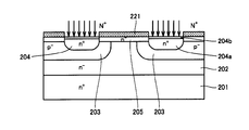
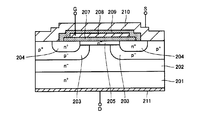
- FIG. 13 and 14 are cross-sectional views showing each manufacturing process of the MOSFET of Patent Document 1.
- FIG. 13 As shown in FIG. 13, n ⁇ epi layer 202 is epitaxially grown on SiC substrate 201. Ions are implanted into the n ⁇ epi layer 202 to form a p ⁇ base region 203.
- An n ⁇ channel layer 205 is epitaxially grown on the n ⁇ epi layer 202 including the p ⁇ base region 203. Thereafter, ion implantation is performed using the LTO film 221 as a mask to form an n + source region 204.
- the time of thermal oxidation for forming the gate oxide film 207 is performed in a later step (see FIG. 14), the area 204b for oxidizing, without oxidizing n + Compared with the region 204a to be left as the source region 204, the n-type impurity concentration is made lower. Thereafter, activation heat treatment is performed.
- the LTO film 221 is removed, a gate oxide film 207 is formed on the surface of the epitaxial layer, and a gate electrode 208 is formed thereon. Further, an insulating film 209 is formed, and a source electrode 210 and a drain electrode 211 are formed.
- Patent Document 1 a p ⁇ base region 203, an n + source region 204 and an n ⁇ channel layer 205 are formed on the surface of the epitaxial layer. If the surface of this epitaxial layer is oxidized to form a gate oxide film, regions of different types and different concentrations of impurities (dopants) are oxidized at once. In this case, the oxidation rate varies depending on the type and concentration of the impurity formed, and the film quality of the gate oxide film may vary. Patent Document 1 describes that suppression of accelerated oxidation in the n + source region 204 is considered, but the region other than the n + source region 204 (n ⁇ channel layer 205) is considered. The formed gate oxide film 207 and the gate oxide film 207 on the n + source region 204 region may have variations in film quality because the ground state is different. When the film quality of the gate oxide film 207 varies, the performance of the MOSFET deteriorates.
- an object of the present invention is to provide a method of manufacturing a SiC semiconductor device capable of improving performance.
- the manufacturing method of the SiC semiconductor device of the present invention includes the following steps.
- An SiC semiconductor including a first surface into which an impurity (dopant) is implanted at least partially is prepared.
- the second surface is formed by cleaning the first surface of the SiC semiconductor.
- a film containing silicon (Si) is formed on the second surface. By oxidizing the film containing Si, an oxide film constituting the SiC semiconductor device is formed.
- the film containing Si since the film containing Si is formed on the second surface formed by cleaning the first surface of the SiC semiconductor, the film containing Si can be cleaned. At the same time, the influence of the second surface on the film quality of the film containing Si can be reduced. For this reason, uniformity of the film quality of the film containing Si can be improved.
- a film containing Si with improved film quality is oxidized, variation in the oxidation rate in the depth direction can be reduced at each position of the film containing Si.
- variations in the quality of an oxide film formed by oxidizing a film containing Si with improved film quality can be reduced. Therefore, since the quality of the oxide film constituting the SiC semiconductor device can be improved, the performance of the SiC semiconductor device can be improved.
- the film containing Si is a SiC film.
- the film containing Si since the crystal of the film containing Si is the same as the crystal of the underlying SiC semiconductor, the film containing Si can be easily formed.
- the Si-containing film is preferably a Si film.
- the step of forming the film containing Si is determined when the thickness of the oxide film constituting the SiC semiconductor device is determined and when all the films containing Si are oxidized. And a step of controlling the thickness of the Si-containing film so as to be the thickness of the oxide film.
- an oxide film having a desired thickness can be formed by controlling the thickness of the film containing Si. Further, by oxidizing so that the film containing Si becomes an oxide film, an oxide film with a reduced content of impurities implanted into the first surface can be formed.
- an oxide film constituting the SiC semiconductor device is formed by oxidizing a film containing Si, so that an SiC semiconductor device capable of improving performance can be manufactured.
- FIG. 10 is a cross-sectional view showing each manufacturing process of a MOSFET of Patent Document 1.
- FIG. 10 is a cross-sectional view showing each manufacturing process of a MOSFET of Patent Document 1.
- FIG. 1 is a schematic diagram of a SiC semiconductor device manufacturing apparatus 10 according to an embodiment of the present invention. Referring to FIG. 1, a SiC semiconductor device manufacturing apparatus 10 according to an embodiment of the present invention will be described.
- the SiC semiconductor device manufacturing apparatus 10 includes a cleaning unit 11, a first forming unit 12, a second forming unit 13, a first connecting unit 14, and a second connecting unit. 15.
- the cleaning unit 11 and the first forming unit 12 are connected by a first connection unit 14.
- the insides of the cleaning unit 11, the first forming unit 12, and the first connecting unit 14 are shielded from the atmosphere, and the insides can communicate with each other.
- the first forming part 12 and the second forming part 13 are connected by a second connecting part 15.
- the insides of the first forming part 12, the second forming part 13, and the second connecting part 15 are shielded from the atmosphere, and the insides can communicate with each other.
- Cleaning unit 11 forms the second surface by cleaning the first surface in which impurities are implanted into at least a part of the SiC semiconductor.
- an H etching apparatus for dry etching hereinafter, also referred to as “H etching”
- H 2 gas containing hydrogen gas
- the H etching apparatus for example, a high frequency heating furnace or the like can be used.
- the cleaning unit 11 is not particularly limited to the H etching apparatus, and an apparatus for cleaning by forming an oxide film on the first surface of the SiC semiconductor and removing the oxide film may be used.
- the apparatus for forming the oxide film and the apparatus for removing the oxide film may be the same or different.
- a connection portion that is shielded from the atmosphere and that connects the SiC semiconductors so as to be transportable is further disposed. .
- the first forming unit 12 forms a film containing Si on the second surface.
- a CVD (Chemical Vapor Deposition) apparatus is used for the first forming unit 12.
- 2nd formation part 13 forms the oxide film which constitutes a SiC semiconductor device by oxidizing the film containing Si.
- a dry oxidation (thermal oxidation) apparatus, a wet oxidation apparatus heated in an oxygen atmosphere containing water vapor, or the like can be used as the second formation unit 13, and a dry oxidation apparatus is preferably used.
- the first connection unit 14 connects the cleaning unit 11 and the first forming unit 12 so that the SiC semiconductor can be transported.
- a region (internal space) in which the epitaxial wafer 100 is transported in the first connection portion 14 can be shielded from the atmosphere.
- the second connecting portion 15 connects the first forming portion 12 and the second forming portion 13 so as to be able to transport a SiC semiconductor in which a film containing Si is formed.
- a region (internal space) in which the epitaxial wafer 100 is transported in the second connection portion 15 can be shut off from the atmosphere.
- the interruption of the atmosphere means an atmosphere in which the atmosphere is not mixed, for example, an atmosphere made of at least one kind of gas such as nitrogen gas, hydrogen gas and inert gas, or a vacuum.
- the atmosphere from which the air is blocked is, for example, nitrogen (N), hydrogen (H), helium (He), neon (Ne), argon (Ar), krypton (Kr), xenon (Xe), radon ( Rn), or an atmosphere filled with a gas composed of a combination of these, or a vacuum.
- the first connection part 14 connects the inside of the cleaning part 11 and the inside of the first forming part 12.
- the first connection unit 14 has a space for transporting the SiC semiconductor unloaded from the cleaning unit 11 to the first forming unit 12. That is, the 1st connection part 14 is installed in order to convey the SiC semiconductor from the washing
- the second connecting portion 15 connects the inside of the first forming portion 12 and the inside of the second forming portion 13.
- Second connecting portion 15 has a space for transporting the SiC semiconductor unloaded from first forming portion 12 to second forming portion 13. That is, the 2nd connection part 15 is installed in order to convey to the 2nd formation part 13 from the 1st formation part 12 so that a SiC semiconductor may not be open
- the first and second connecting portions 14 and 15 have such a size that the SiC semiconductor can be transported inside. Moreover, the 1st and 2nd connection parts 14 and 15 may have a magnitude
- 1st connection part 14 is a load lock room which connects the exit of cleaning part 11 and the entrance of the 1st formation part 12, for example.
- the second connecting portion 15 is a load lock chamber that connects, for example, the outlet of the first forming portion 12 and the inlet of the second forming portion 13.
- the manufacturing apparatus 10 may further include a first transport unit that is disposed inside the first connection unit 14 and transports the SiC semiconductor from the cleaning unit 11 to the first formation unit 12. Good.
- the manufacturing apparatus 10 further includes a second transport unit that is disposed inside the second connection unit 15 and transports the SiC semiconductor from the first formation unit 12 to the second formation unit 13. Also good.
- the first transport unit and the second transport unit may be the same or different.
- the manufacturing apparatus 10 may further include a first blocking unit that is disposed in the first connecting unit 14 and that blocks the inside of the cleaning unit 11 and the inside of the first forming unit 12. Good.
- the manufacturing apparatus 10 further includes a second blocking unit that is disposed in the second connecting unit 15 and that blocks the inside of the first forming unit 12 and the inside of the second forming unit 13. May be.
- the first and second blocking portions for example, a valve or a door that can block each communicating portion can be used, and a plurality of the first and second blocking portions may be provided.
- the manufacturing apparatus 10 may further include a vacuum pump for discharging the internal atmospheric gas and a replacement gas cylinder for replacing the internal atmospheric gas.
- the vacuum pump and the replacement gas cylinder may be connected to each of the cleaning unit 11, the first forming unit 12, the second forming unit 13, the first connecting unit 14, and the second connecting unit 15. Or may be connected to one.
- the manufacturing apparatus 10 may include various elements other than the above, illustration and description of these elements are omitted for convenience of explanation.
- the 1st connection part 14 connects only between the washing
- the shape which connects only between 13 was shown, it is not limited to this in particular.
- the first and second connection portions 14 and 15 for example, a chamber in which the atmosphere is shut off is used, and the cleaning portion 11, the first formation portion 12, and the second formation portion 13 are disposed in the chamber. Good.
- FIG. 2 is a flowchart showing a method for manufacturing the SiC semiconductor device according to the embodiment of the present invention.
- 3 to 8 are cross-sectional views schematically showing each manufacturing process of the SiC semiconductor device according to the embodiment of the present invention.
- FIG. 9 is a cross sectional view schematically showing a SiC semiconductor device manufactured in the embodiment of the present invention. In the present embodiment, a method of manufacturing MOSFET 101 shown in FIG. 9 as an SiC semiconductor device using SiC semiconductor device manufacturing apparatus 10 shown in FIG. 1 will be described.
- SiC substrate 2 is prepared (step S1).
- SiC substrate 2 is not particularly limited, but can be prepared, for example, by the following method.
- a SiC ingot grown by a vapor phase growth method such as a sublimation method or a CVD method, a liquid phase growth method, or the like is prepared. Thereafter, a SiC substrate having a surface is cut out from the SiC ingot.
- the cutting method is not particularly limited, and the SiC substrate is cut from the SiC ingot by slicing or the like.
- the surface of the cut SiC substrate is polished.
- the surface to be polished may be only the front surface, or the back surface opposite to the front surface may be further polished.
- the polishing method is not particularly limited, but CMP (Chemical Mechanical Polishing), for example, can be employed to flatten the surface and reduce damage such as scratches.
- CMP Chemical Mechanical Polishing
- colloidal silica is used as an abrasive, and an adhesive, wax, or the like is used as a fixing agent.
- other polishing such as an electric field polishing method, a chemical polishing method, and a mechanical polishing method may be further performed. Polishing may be omitted.
- the cleaning method is not particularly limited. For example, after the oxide film is formed by thermal oxidation or the like, cleaning by removing the oxide film by thermal decomposition or thermal etching can be employed. The cleaning of the SiC substrate may be omitted.
- the SiC substrate 2 shown in FIG. 3 can be prepared.
- SiC substrate 2 for example, a substrate having an n-type conductivity and a resistance of 0.02 ⁇ cm is used.
- an epitaxial layer is formed on the SiC substrate 2 by a vapor phase growth method, a liquid phase growth method, or the like (step S2).
- the epitaxial layer is formed as follows.
- the buffer layer 121 is formed on the SiC substrate 2.
- Buffer layer 121 is an epitaxial layer made of, for example, n-type SiC and having a thickness of 0.5 ⁇ m, for example.
- the concentration of the n-type conductive impurity in the buffer layer 121 is, for example, 5 ⁇ 10 17 cm ⁇ 3 .
- the drift layer 122 is formed on the buffer layer 121.
- drift layer 122 a layer made of SiC of n-type conductivity is formed by vapor phase growth, liquid phase growth, or the like.
- the thickness of drift layer 122 is, for example, 10 ⁇ m.
- the concentration of the n-type conductive impurity in drift layer 122 is, for example, 5 ⁇ 10 15 cm ⁇ 3 .
- p body region 123, n + source region 124, and p + region 125 shown in FIG. 4 are formed as follows. First, a body region 123 is formed by selectively injecting a p-type impurity into part of the drift layer 122. Thereafter, a source region 124 is formed by selectively injecting n-type conductive impurities into a predetermined region, and p-type by selectively injecting p-type conductive impurities with a p-type conductivity into the predetermined region. A + region 125 is formed. Note that the selective implantation of conductive impurities is performed using a mask made of an oxide film, for example, and is removed after the implantation.
- each implantation profile takes into account the thickness removed by cleaning in step S4 described later. That is, the ion implantation is controlled so that the impurity diffusion region is in a desired arrangement when the first surface of the epitaxial layer is removed in the cleaning step S4.
- an activation annealing process may be performed.
- annealing is performed in an argon atmosphere at a heating temperature of 1700 ° C. for 30 minutes.
- the epitaxial wafer 100 provided with 120 can be prepared.
- first surface 120a of epitaxial layer 120 has regions in which at least one of the kind and concentration of impurities is different.
- the first surface 120a of the epitaxial wafer 100 is cleaned to form the second surface 120b (step S4).
- the cleaning method is not particularly limited, and for example, a method of dry etching (H etching) using a gas containing hydrogen gas, a method of forming an oxide film and removing this oxide film, and the like can be adopted. It is preferable to employ H etching.
- the first surface 120a of the epitaxial layer 120 is dry-etched with hydrogen gas, and impurities, particles, and the like attached to the first surface 120a are removed together with the first surface 120a.
- the clean second surface 120b shown in FIG. 5 can be formed by removing the first surface 120a.
- H etching is preferably performed in a temperature range of 1300 ° C. or higher and 1650 ° C. or lower.
- the etching rate can be increased, and by performing the etching at a temperature of 1650 ° C. or lower, it is possible to suppress an excessive increase in the etching rate, so that the etching amount can be easily controlled. . Therefore, by adjusting the temperature condition of the H etching to 1300 ° C. or more and 1650 ° C. or less, it is possible to control the etching rate to a suitable etching rate. Therefore, the first surface 120a can be H-etched with high accuracy.
- the quality of the MOSET 101 see FIG.
- Such temperature setting is performed, for example, by heating the epitaxial wafer 100 disposed in the H etching apparatus to 1300 ° C. or higher and 1650 ° C. or lower and etching gas (hereinafter referred to as “etching gas”) of 1300 ° C. or higher and 1650 ° C. or lower.
- etching gas etching gas
- the flow rate of hydrogen gas during H etching is not particularly limited, but is preferably about several hundred slm (standard liter per minute).
- the pressure during H etching is preferably about several tens hPa to several hundreds hPa. In this case, H etching can be performed at a preferable rate.
- the etching gas only hydrogen gas may be used, or a mixed gas of hydrogen gas and another gas may be used.
- a mixed gas in which hydrogen chloride (HCl) gas is mixed with hydrogen gas By using such a mixed gas, the etching rate can be increased. If the content of hydrogen chloride gas in the mixed gas is too high, the etching rate becomes too high and it becomes difficult to control the etching. Therefore, the content of hydrogen chloride gas in the mixed gas is preferably 10% or less.
- the hydrogen chloride gas content (hydrogen chloride gas / (hydrogen chloride gas + hydrogen gas) ⁇ 100) in the mixed gas composed of hydrogen chloride gas and hydrogen gas is more preferably 10% or less.
- the mixed gas which mixed hydrocarbon gas with hydrogen gas.
- etching can be performed while improving the surface morphology of the epitaxial wafer 100, and the second surface 120b having a good surface state can be formed.
- the hydrocarbon lower hydrocarbons such as alkanes and alkenes can be used.
- acetylene (C 2 H 2 ) and propane (C 3 H 8 ) can be used.
- Such hydrocarbon gas is preferably mixed at 1000 ppm or less in order to effectively exhibit the effect of suppressing the generation of Si droplets.
- a mixed gas obtained by mixing hydrogen gas, hydrogen chloride gas, and hydrocarbon gas may be used as the etching gas.
- Step S4 In the case of performing the H etching, by using the manufacturing apparatus 10 shown in FIG. 1, after the step of forming the second surface 120b (step S4), without using a liquid phase for cleaning, Si described later is used. Step S5 for forming the film 128 containing can be performed. Thereby, adhesion of impurities (particularly heavy metal ions and alkali ions) resulting from cleaning using the liquid phase can be suppressed.
- the cleaning using the liquid phase means that the epitaxial wafer as the SiC semiconductor is cleaned in the liquid phase, and may include an unintended gas phase component.
- the method for oxidizing the first surface 120a is not particularly limited.
- a solution containing O, thermal oxidation in an atmosphere containing O gas, O plasma, or the like can be used.
- the solution containing O means a solution containing oxygen (O), for example, ozone water.
- O oxygen
- ozone water having a concentration of, for example, 30 ppm or more. In this case, the decomposition of ozone can be suppressed, and the reaction speed between the first surface 120a of the epitaxial wafer 100 and ozone can be increased, so that an oxide film can be easily formed on the first surface 120a.
- O gas means a gas containing oxygen, and thermal oxidation in an atmosphere containing O gas is performed in a dry atmosphere at a temperature of 700 ° C. or higher, considering that SiC is a stable compound. Is preferred.
- the dry atmosphere means that an oxide film is formed in the gas phase, and may include an unintended liquid phase component.
- O plasma means plasma generated from a gas containing oxygen, and can be generated, for example, by supplying oxygen gas (O 2 ) to a plasma generator.
- Oxide film is formed by O plasma means that an oxide film is formed by plasma using a gas containing oxygen. In other words, it means that an oxide film is formed by processing with plasma generated from a gas containing oxygen.
- the method for removing the oxide film formed on the first surface 120a is not particularly limited, and for example, wet etching, dry etching, thermal decomposition, F plasma, or the like can be used.
- the oxide film is removed using a solution such as HF or NH 4 F (ammonium fluoride).
- the oxide film In dry etching, it is preferable to remove the oxide film using at least one of hydrogen gas and hydrogen chloride gas at a temperature of 1000 ° C. or higher and lower than the sublimation temperature of SiC. Hydrogen gas and hydrogen chloride gas at 1000 ° C. or higher have a high effect of reducing the oxide film.
- the oxide film is SiO x
- hydrogen gas decomposes SiO x into H 2 O and SiH y
- hydrogen chloride gas decomposes SiO x into H 2 O and SiCl z .
- Deterioration of the epitaxial wafer 100 can be suppressed by setting the temperature to a sublimation temperature of SiC or lower.
- dry etching is preferably performed under reduced pressure from the viewpoint of promoting the reaction.
- the thermal decomposition is preferably performed by thermally decomposing the oxide film at a temperature not lower than 1200 ° C. and not higher than the sublimation temperature of SiC in an atmosphere not containing oxygen.
- the oxide film formed on the first surface 120a of the epitaxial wafer 100 is heated in an atmosphere containing no oxygen at 1200 ° C. or higher, the oxide film can be easily pyrolyzed.
- Degradation of the epitaxial wafer 100 can be suppressed by setting the temperature to a sublimation temperature of SiC or lower.
- F plasma means plasma generated from a gas containing fluorine (F), for example, carbon tetrafluoride gas (CF 4 ), trifluoromethane gas (CHF 3 ), Freon gas (C 2 F 6 ), six Sulfur fluoride gas (SF 6 ), nitrogen trifluoride gas (NF 3 ), xenon difluoride gas (XeF 2 ), fluorine gas (F 2 ), and chlorine trifluoride gas (ClF 3 ) alone or It can generate
- “Removing the oxide film by F plasma” means removing the oxide film by plasma using a gas containing fluorine. In other words, it means that the oxide film is removed by processing with plasma generated from a gas containing fluorine.
- the etching depth in the case of cleaning by H etching (etching in the direction from the first surface 120a to the SiC substrate 2).
- Amount) and the thickness of the oxide film formed in the cleaning by forming and removing the oxide film is, for example, not less than one molecular layer and not more than 10 nm. .
- the etching depth in the case of cleaning by H-etching, and the oxide film (sacrificial oxide film) in the case of cleaning by formation (sacrificial oxide film formation step) and removal (sacrificial oxide film removal step) of the oxide film The thickness of is, for example, larger than 10 nm and not larger than 500 nm. Accordingly, impurities, particles, and the like attached to the first surface 120a can be removed, and a rough region can be removed, so that the second surface 120b having excellent surface characteristics can be formed.
- the epitaxial wafer 100 on which the second surface 120 b is formed by the cleaning unit 11 is transferred to the first forming unit 12.
- the epitaxial wafer 100 is transferred in the first connection portion 14 which is an atmosphere in which the air is blocked.
- the epitaxial wafer 100 is placed in an atmosphere in which air is blocked.
- a film 128 containing Si is formed on the second surface 120b after the cleaning of the epitaxial wafer 100 (step S5). Since the second surface 120b is cleaned, the cleanliness of the film 128 formed thereon can be improved. In addition, since the film 128 is formed over the second surface 120b, the influence of the type and concentration of impurities formed on the second surface 120b can be reduced, so that the film 128 with improved quality uniformity is formed. be able to.
- the method for forming the Si-containing film 128 on the second surface 120b is not particularly limited.
- a known epitaxial growth method can be used, and a CVD method is preferably used.
- the CVD method since the film 128 is stacked on the second surface 120b, the influence of the doped state such as the type and concentration of impurities on the second surface 120b of the underlying epitaxial wafer 100 can be further reduced. .
- a Si film or a SiC film as the film 128.
- the Si film is composed mainly of Si, for example, and the remainder is made of inevitable impurities.
- the SiC film is composed mainly of SiC, for example, and the remainder is made of inevitable impurities.
- a Si film is formed as the film 128, it is possible to suppress the presence of C in the interface between the epitaxial wafer 100 and the gate oxide film 126 and in the gate oxide film 126. Therefore, the quality of the MOSFET 101 to be manufactured (FIG. 9) Can be further enhanced.
- the film 128 is SiC
- the crystal of the underlying epitaxial layer 120 and the formed film 128 are the same (that is, the lattice constants of the epitaxial layer 120 and the film 128 are the same), so the film 128 is easily formed. can do.
- the thickness of the gate oxide film 126 (see FIG. 7) formed in step S6 described later is determined, and when the film 128 is entirely oxidized (without oxidizing the epitaxial layer 120 under the film 128), It is preferable to control the thickness of the film 128 so that the determined thickness of the gate oxide film 126 is obtained. That is, it is preferable to determine the thickness of the film 128 to be formed in accordance with the thickness of the gate oxide film 126 formed by oxidizing the film 128. This can be realized by controlling the thickness of the film 128 by calculation or the like in consideration of an increase in film thickness due to oxygen incorporation when the film 128 is oxidized to become the gate oxide film 126.
- the thickness of the film 128 is about 0.44 times the thickness of the gate oxide film 126 (see FIG. 7) to be formed. That is, in this step S5, a Si film having a thickness of about 0.44 times the thickness of the gate oxide film 126 formed in step S6 is formed as the film 128.
- the thickness of the gate oxide film 126 can be set to the designed thickness even if the film 128 is oxidized to become a gate oxide film and the film thickness is increased by incorporating oxygen. It can be.
- the epitaxial wafer 100 on which the film 128 containing Si is formed in the first forming unit 12 is transferred to the second forming unit 13.
- the epitaxial wafer 100 is transferred in the second connection portion 15 which is an atmosphere in which the atmosphere is blocked.
- the epitaxial wafer 100 is placed in an atmosphere in which the atmosphere is blocked. Thereby, impurities contained in the atmosphere can be prevented from adhering to the film 128.
- a gate oxide film 126 as an oxide film constituting the SiC semiconductor device is formed (step S6).
- the gate oxide film 126 is silicon oxide (SiO x ).
- the method for oxidizing the film 128 is not particularly limited, but is preferably performed in an atmosphere containing oxygen, such as dry oxidation or wet oxidation, and is preferably dry oxidation.
- the dry oxidation conditions are, for example, a heating temperature of 1200 ° C. and a heating time of 30 minutes.
- Such oxidation can be performed by, for example, putting the film into the oxidation furnace after step S5 for forming the film 128 and adjusting the heating temperature and the heating time.
- step S6 it is preferable to form the gate oxide film 126 by oxidizing all the film 128 formed in step S5. Thereby, the remaining film 128 can be reduced.
- step S6 it is more preferable to form the gate oxide film 126 by oxidizing only the film 128 formed in step S5 (without oxidizing the epitaxial wafer 100).
- the gate oxide film 126 can be formed so as not to include impurities of the epitaxial wafer 100 ion-implanted in step S3, the quality of the gate oxide film 126 can be improved. Further, the influence on the ion implantation profile of the epitaxial layer 120 can be reduced.
- the gate oxide film 126 is annealed (step S7).
- this step S7 for example, at least one of nitriding treatment and inert gas annealing treatment can be performed on the gate oxide film 126.
- nitriding treatment heat treatment is performed in an atmosphere containing nitrogen.
- annealing can be performed for 120 minutes at a heating temperature of 1200 ° C. in a nitrogen monoxide (NO) atmosphere or an oxygen dinitride (N 2 O) atmosphere.
- NO nitrogen monoxide
- N 2 O oxygen dinitride
- inert gas annealing treatment heat treatment is performed in an atmosphere containing an inert gas.
- annealing can be performed in an inert gas atmosphere such as argon (Ar) at a heating temperature of 1100 ° C. for 60 minutes.
- nitriding treatment and inert gas annealing treatment When the above nitriding treatment and inert gas annealing treatment are performed, high channel mobility reproducibility can be improved in the MOSFET 101. Note that only one of the nitriding treatment and the inert gas annealing treatment may be performed, and step S7 may be omitted. When performing nitriding and inert gas annealing, it is preferable to perform inert gas annealing after nitriding.
- step S7 surface cleaning such as organic cleaning, acid cleaning, RCA cleaning, and the like may be further performed.
- an electrode is formed on the epitaxial wafer on which the gate oxide film 126 is formed (step S8).
- the source electrode 111 shown in FIG. 8 is formed as follows. Specifically, a resist film having a pattern is formed on the gate oxide film 126 by using a photolithography method. Using this resist film as a mask, portions of gate oxide film 126 located on n + source region 124 and p + region 125 are removed by etching. Thereby, an opening is formed in the gate oxide film 126. For example, a conductive film is formed by vapor deposition so as to be in contact with each of n + source region 124 and p + region 125 in this opening. Next, by removing the resist film, the portion of the conductor film located on the resist film is removed (lifted off).
- the conductor film may be a metal film, and is made of nickel (Ni), for example. As a result of this lift-off, the source electrode 111 is formed.
- the heat processing for alloying is performed here.
- heat treatment is performed for 2 minutes at a heating temperature of 950 ° C. in an atmosphere of argon (Ar) gas that is an inert gas.
- an upper source electrode 127 is formed on the source electrode 111 by, for example, vapor deposition.
- drain electrode 112 is formed on the back surface of SiC substrate 2 by, for example, vapor deposition.
- the gate electrode 110 is formed as follows, for example. A resist film having an opening pattern located in a region on the gate oxide film 126 is formed in advance, and a conductor film constituting a gate electrode is formed so as to cover the entire surface of the resist film. Then, by removing the resist film, the conductor film other than the portion of the conductor film to be the gate electrode is removed (lifted off). As a result, the gate electrode 110 can be formed on the gate oxide film 126 as shown in FIG.
- step S3 you may carry out by adding the wet washing process using a chemical
- the chemical solution include SPM containing sulfuric acid and hydrogen peroxide solution.
- epitaxial wafer 100 is prepared as an SiC semiconductor including first surface 120a into which impurities are implanted at least partially.
- a process steps S1 to S3
- a process step S4 of forming the second surface 120b by cleaning the first surface 120a of the epitaxial wafer 100, and a film containing Si on the second surface 120b.
- a step of forming 128 step S5
- a step of forming the gate oxide film 126 as an oxide film constituting the MOSFET 101 as the SiC semiconductor device by oxidizing the film 128 containing Si step S7. ing.
- second surface 120b has different doping concentrations and different types of dopant regions. Even if it has, the influence of the 2nd surface 120b can be reduced about the film quality of the film
- the manufacturing method of the present embodiment includes a region that is easily oxidized and a region that is not easily oxidized. The difference can be reduced. Therefore, the quality of the gate oxide film 126 can be improved.
- the film 128 containing Si is formed on the second surface 120b formed by cleaning the first surface 120a of the epitaxial wafer 100, the cleaning of the film 128 can be improved. Therefore, the cleaning of the gate oxide film 126 formed on the film 128 can be enhanced. Specifically, impurities, particles, etc. existing at the interface between the epitaxial wafer 100 and the gate oxide film 126 can be reduced. Further, impurities, particles and the like existing in the gate oxide film 126 can be reduced, and the film quality of the gate oxide film 126 can be improved. Therefore, the breakdown voltage when the reverse voltage is applied to the MOSFET 102 having the gate oxide film 126 can be improved, and the stability and long-term reliability of the operation when the forward voltage is applied can be improved.
- a uniform Si-containing film 128 is formed on the clean second surface 120b, and the film 128 is oxidized, so that a uniform and clean gate oxide film 126 can be formed.
- MOSFET 101 that can improve the above can be manufactured.
- dry etching is preferably performed using a gas containing hydrogen gas in step S4 for cleaning.
- the first surface 120a can be removed by H-etching the first surface 120a of the epitaxial wafer 100.
- the second surface 120b can be formed with higher cleaning.
- SiC is a stable compound, so that damage to the epitaxial wafer 100 is small. For this reason, the 2nd surface 120b with favorable surface characteristics can be formed. Therefore, a SiC semiconductor device with improved quality can be manufactured.
- step S4 H etching is performed, and after the step of forming second surface 120b (step S4), the liquid phase The step of forming the film 128 (step S5) is performed without cleaning using.
- the present inventor has not only insufficiently cleaned the epitaxial wafer 100 when the epitaxial wafer 100 is cleaned using the liquid phase, but also causes impurities due to the liquid phase to adhere. I found out. For this reason, after forming the second surface 120b, by forming the film 128 without cleaning using the liquid phase, impurities such as alkali ions and heavy metal ions caused by the cleaning using the liquid phase are formed. Adhesion can be prevented.
- Higher quality MOSFET 101 can be manufactured by reducing alkali ions, heavy metal ions, and the like.
- the cleaning time of about 15 hours is required, but the cleaning using the liquid phase is not included.
- the first surface 120a of the epitaxial wafer 100 can be cleaned in about 4 hours. Therefore, in the method of manufacturing the SiC semiconductor device according to the present embodiment, cleaning using a liquid phase, sacrificial oxidation, and sacrificing are performed between the cleaning by H etching (step S2) and the formation of the film 128 (step S5). By not removing the oxide film, the manufacturing time of the SiC semiconductor device can be shortened.
- step S5 the step of forming the Si-containing film 128 (step S5) is performed after the step of forming the second surface 120b (step S4) without cleaning using the liquid phase” is used. It means that cleaning using a liquid phase is not included between step S4 and step S5, and between step S4 and step S5 may be performed intermittently (time may elapse). . Moreover, you may perform step S4 and step S5 continuously.
- a MOSFET manufacturing method has been described as an example of the SiC semiconductor device, but the present invention cleans the SiC epitaxial wafer including the first surface 120a in which impurities are implanted at least partially, SiC having a structure obtained by oxidizing the film 128 containing Si formed on the second surface 120b obtained by cleaning the first surface 120a (comprising an oxide film remaining as a SiC semiconductor device)
- the present invention can be applied to a semiconductor device manufacturing method.
- the present invention relates to a SiC semiconductor device having an insulated gate field effect portion such as a MOSFET or IGBT (Insulated Gate Bipolar Transistor), or an oxidation of a JFET (Junction Field-Effect Transistor).
- the present invention can be applied to all SiC semiconductor devices having a film.
- FIG. 10 is a cross-sectional view schematically showing an epitaxial wafer used in Samples 1 to 3 in the example.
- Example 1 Specifically, first, a 4H—SiC substrate was prepared as the SiC substrate 2 (step S1). Next, an n-type SiC layer 131 having a thickness of 10 ⁇ m and an impurity concentration of 1 ⁇ 10 16 cm ⁇ 3 was grown by CVD as a layer constituting the epitaxial layer 120 (step S2).
- p body region 123 having a conductive impurity concentration of 2 ⁇ 10 16 cm ⁇ 3 is formed using aluminum (Al) as a p-type impurity, and phosphorus (P) is further added to n
- An n + source region 124 having a conductive impurity concentration of 1 ⁇ 10 19 cm ⁇ 3 was formed as a type impurity.
- a p + region 125 having a conductive impurity concentration of 1 ⁇ 10 19 cm ⁇ 3 was formed using Al as a p-type impurity (step S3). Note that the mask was removed after each ion implantation.
- activation annealing treatment was performed.
- Ar gas Ar 2
- the heating temperature was 1700 to 1800 ° C. and the heating time was 30 minutes.
- an epitaxial wafer 130 having a first surface 130a in which impurities were implanted at least partially was prepared.
- the first surface 130a of the prepared epitaxial wafer 100 was removed by H etching (step S4).
- the epitaxial wafer 130 was accommodated in a reaction furnace, and the first surface 130a was H-etched while heating the epitaxial wafer 130 on a mounting table controlled at 1300 ° C. or higher and 1650 ° C. or lower.
- the H etching conditions were such that the flow rate of hydrogen gas introduced into the reaction furnace was 50 to 200 slm, the furnace pressure was 20 to 150 hPa, and the reaction time was 1 hour.
- Sample 2 was basically the same as Sample 1, but differed in that the H etching in Step S2 was not performed. That is, in Sample 2, the cleaning process was not performed on the epitaxial wafer 130 prepared in Steps S1 to S3.
- the sample 3 was basically the same as the sample 1 except that the first surface 130a of the epitaxial wafer 130 was cleaned in step S2 using a liquid phase instead of H etching.
- a liquid phase a mixed solution 1 in which sulfuric acid: hydrogen peroxide solution was mixed at a volume ratio of 5: 1; a mixed solution 2 in which ammonia water: hydrogen peroxide solution: pure water was mixed at a volume ratio of 1: 1: 5;
- a mixed solution 3 in which hydrogen (HCl): hydrogen peroxide (H 2 O 2 ): pure water was mixed at a volume ratio of 1: 1: 6 and a 10% hydrogen fluoride (HF) solution were used.
- the prepared epitaxial wafer 130 was immersed in the mixed solution 1 for 0.5 hour, then immersed in the mixed solution 2 for 10 minutes, immersed in the HF solution for 10 minutes, and immersed in the mixed solution 3 for 10 minutes. Then, it was immersed in the mixed solution 2 for 10 minutes and immersed in the HF solution for 10 minutes to perform chemical cleaning.
- the epitaxial wafer 130 after the chemical cleaning was dried by blowing with Ar gas or N 2 gas using an Ar gun or N 2 gun.
- TXRF total reflection X-ray fluorescence analysis
- Impurities were measured on the surfaces of the epitaxial wafers 130 of Samples 1 to 3 by TXRF. Impurities were reduced in the surface of the epitaxial wafer 130 after the H etching in the sample 1 as compared with the surface of the sample 2 in which the H etching was not performed. Therefore, a SiC semiconductor device with improved quality can be manufactured by forming a film containing Si on the epitaxial wafer 130 after H etching and oxidizing the film to form an oxide film constituting the SiC semiconductor device. I understand.
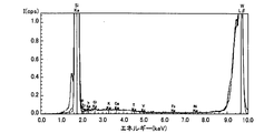
- FIG. 11 is a spectrum showing a result of measuring the surface of the epitaxial wafer 130 of the sample 2 by TXRF
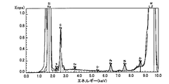
- FIG. 12 is a spectrum showing a result of measuring the surface of the epitaxial wafer 130 after the cleaning of the sample 3 by TXRF.
- the horizontal axis indicates the energy intensity
- the vertical axis indicates the spectrum intensity. The larger the peak height, the more detected the intensity.
- “Cl, Ka” described in FIG. 11 indicates that a Cl—K ⁇ ray has been detected, and other descriptions are the same.
- the peak in the vicinity of the energy intensity of 9.67 eV is a peak of the WL line that is an excitation ray source.
- the epitaxial wafer 130 after the H etching in the sample 1 is not cleaned using a liquid phase, but a film containing Si is formed, and this film is oxidized to form an oxide film. It has been found that manufacturing a semiconductor device provided as can improve the quality and manufacture a SiC semiconductor device.
- SiC substrate 10 manufacturing equipment, 11 cleaning section, 12 first forming section, 13 second forming section, 14 first connecting section, 15 second connecting section, 100, 130 epitaxial wafer, 120a, 130a first 1 surface, 120b second surface, 101 MOSFET, 110 gate electrode, 111, 127 source electrode, 112 drain electrode, 120 epitaxial layer, 121 buffer layer, 122 drift layer, 123 body region, 124 source region, 125 p + Region, 126 gate oxide film, 128 film, 131 SiC layer.
Landscapes
- Engineering & Computer Science (AREA)
- Microelectronics & Electronic Packaging (AREA)
- Power Engineering (AREA)
- Physics & Mathematics (AREA)
- Condensed Matter Physics & Semiconductors (AREA)
- General Physics & Mathematics (AREA)
- Computer Hardware Design (AREA)
- Manufacturing & Machinery (AREA)
- Chemical & Material Sciences (AREA)
- Crystallography & Structural Chemistry (AREA)
- Ceramic Engineering (AREA)
- Electrodes Of Semiconductors (AREA)
- Recrystallisation Techniques (AREA)
- Formation Of Insulating Films (AREA)
- Drying Of Semiconductors (AREA)
- Cleaning Or Drying Semiconductors (AREA)
Abstract
Description
これにより、SiC半導体層と酸化膜との界面および酸化膜中に炭素(C)が存在することを抑制できるので、製造するSiC半導体装置の性能をより向上することができる。
具体的には、まず、SiC基板2として、4H-SiC基板を準備した(ステップS1)。次に、エピタキシャル層120を構成する層として、10μmの厚みを有し、1×1016cm-3の不純物濃度を有するn型SiC層131をCVD法により成長した(ステップS2)。
試料2は、基本的には試料1と同様であったが、ステップS2のHエッチングを行なわなかった点において異なっていた。すなわち、試料2では、ステップS1~3で準備したエピタキシャルウエハ130に対しては、洗浄処理を行なわなかった。
試料3は基本的には試料1と同様であったが、ステップS2において、Hエッチングのかわりに液相を用いてエピタキシャルウエハ130の第1の表面130aを洗浄した点において異なっていた。液相として、硫酸:過酸化水素水を5:1の体積比で混合した混合溶液1と、アンモニア水:過酸化水素水:純水を1:1:5の体積した混合溶液2と、塩化水素(HCl):過酸化水素(H2O2):純水を1:1:6の体積比で混合した混合溶液3と、10%のフッ化水素(HF)溶液とを用いた。すなわち、試料3では、準備したエピタキシャルウエハ130を混合溶液1に0.5時間浸漬した後、混合溶液2に10分間浸漬し、HF溶液に10分時間浸漬し、混合溶液3に10分間浸漬し、混合溶液2に10分間浸漬し、HF溶液に10分間浸漬して、薬液洗浄を行なった。なお、薬液洗浄後のエピタキシャルウエハ130は、ArガンまたはN2ガンを用いて、ArガスまたはN2ガスでブローすることよって乾燥させた。
試料1~3のエピタキシャルウエハ130の表面を、TXRF(全反射蛍光X線分析法)に供した。なお、TXRFにおいて、励起源としてW(タングステン)-Lβ線を用いた。
Claims (4)
- 炭化珪素半導体装置(101)を製造する方法であって、
少なくとも一部に不純物が注入された第1の表面(120a)を含む炭化珪素半導体(100)を準備する工程と、
前記炭化珪素半導体(100)の前記第1の表面(120a)を洗浄することにより、第2の表面(120b)を形成する工程と、
前記第2の表面(120b)上に珪素を含む膜(128)を形成する工程と、
前記珪素を含む膜(128)を酸化することにより、前記炭化珪素半導体装置(101)を構成する酸化膜(126)を形成する工程とを備えた、炭化珪素半導体装置(101)の製造方法。 - 前記珪素を含む膜(128)が炭化珪素膜である、請求項1に記載の炭化珪素半導体装置(101)の製造方法。
- 前記珪素を含む膜(128)が珪素膜である、請求項1に記載の炭化珪素半導体装置(101)の製造方法。
- 前記珪素を含む膜(128)を形成する工程は、
前記炭化珪素半導体装置(101)を構成する前記酸化膜(126)の厚みを決定する工程と、
前記珪素を含む膜(128)をすべて酸化したときに、決定した前記酸化膜(126)の厚みになるように、前記珪素を含む膜(128)の厚みを制御する工程とを含む、請求項1に記載の炭化珪素半導体装置(101)の製造方法。
Priority Applications (5)
| Application Number | Priority Date | Filing Date | Title |
|---|---|---|---|
| EP11795442.0A EP2584595B1 (en) | 2010-06-16 | 2011-02-25 | Silicon carbide semiconductor device manufacturing method |
| KR1020127011250A KR20130083821A (ko) | 2010-06-16 | 2011-02-25 | 탄화규소 반도체 장치의 제조 방법 |
| CN2011800045863A CN102934210A (zh) | 2010-06-16 | 2011-02-25 | 用于制造碳化硅半导体器件的方法 |
| US13/502,991 US8642476B2 (en) | 2010-06-16 | 2011-02-25 | Method for manufacturing silicon carbide semiconductor device |
| CA2781167A CA2781167A1 (en) | 2010-06-16 | 2011-02-25 | Method for manufacturing silicon carbide semiconductor device |
Applications Claiming Priority (2)
| Application Number | Priority Date | Filing Date | Title |
|---|---|---|---|
| JP2010136872A JP2012004275A (ja) | 2010-06-16 | 2010-06-16 | 炭化珪素半導体装置の製造方法 |
| JP2010-136872 | 2010-06-16 |
Publications (1)
| Publication Number | Publication Date |
|---|---|
| WO2011158534A1 true WO2011158534A1 (ja) | 2011-12-22 |
Family
ID=45347946
Family Applications (1)
| Application Number | Title | Priority Date | Filing Date |
|---|---|---|---|
| PCT/JP2011/054333 WO2011158534A1 (ja) | 2010-06-16 | 2011-02-25 | 炭化珪素半導体装置の製造方法 |
Country Status (8)
| Country | Link |
|---|---|
| US (1) | US8642476B2 (ja) |
| EP (2) | EP2835819A3 (ja) |
| JP (1) | JP2012004275A (ja) |
| KR (1) | KR20130083821A (ja) |
| CN (1) | CN102934210A (ja) |
| CA (1) | CA2781167A1 (ja) |
| TW (1) | TW201203385A (ja) |
| WO (1) | WO2011158534A1 (ja) |
Families Citing this family (7)
| Publication number | Priority date | Publication date | Assignee | Title |
|---|---|---|---|---|
| US9040393B2 (en) * | 2010-01-14 | 2015-05-26 | Taiwan Semiconductor Manufacturing Company, Ltd. | Method of forming semiconductor structure |
| US9165768B2 (en) * | 2011-12-16 | 2015-10-20 | Lg Innotek Co., Ltd. | Method for deposition of silicon carbide and silicon carbide epitaxial wafer |
| JP6418794B2 (ja) * | 2014-06-09 | 2018-11-07 | 東京エレクトロン株式会社 | 改質処理方法及び半導体装置の製造方法 |
| JP2016127177A (ja) * | 2015-01-06 | 2016-07-11 | 住友電気工業株式会社 | 炭化珪素基板、炭化珪素半導体装置および炭化珪素基板の製造方法 |
| WO2017006594A1 (ja) * | 2015-07-08 | 2017-01-12 | 住友電気工業株式会社 | 炭化珪素半導体基板および炭化珪素半導体装置の製造方法 |
| US20180233574A1 (en) * | 2017-02-10 | 2018-08-16 | Purdue Research Foundation | Silicon carbide power transistor apparatus and method of producing same |
| CN115295407B (zh) * | 2022-09-29 | 2023-07-07 | 浙江大学杭州国际科创中心 | 一种SiC功率器件的栅氧结构制备方法和栅氧结构 |
Citations (7)
| Publication number | Priority date | Publication date | Assignee | Title |
|---|---|---|---|---|
| JPH0766192A (ja) * | 1992-06-05 | 1995-03-10 | Cree Res Inc | 炭化ケイ素表面に高品質パッシベーション層を形成する方法及びパッシベーション領域を有する炭化ケイ素基材のデバイス構造 |
| JPH0851110A (ja) * | 1994-08-05 | 1996-02-20 | Matsushita Electric Ind Co Ltd | 絶縁膜の形成方法 |
| JP2000353670A (ja) * | 1999-06-10 | 2000-12-19 | Nec Corp | 半導体装置の製造方法 |
| JP2002270837A (ja) * | 2001-03-12 | 2002-09-20 | Denso Corp | 炭化珪素半導体装置及びその製造方法 |
| JP2006128479A (ja) * | 2004-10-29 | 2006-05-18 | Shikusuon:Kk | 絶縁膜の形成方法および炭化珪素半導体装置 |
| JP2006351744A (ja) * | 2005-06-15 | 2006-12-28 | Fuji Electric Holdings Co Ltd | 炭化珪素半導体装置の製造方法 |
| JP2008294204A (ja) | 2007-05-24 | 2008-12-04 | Denso Corp | 炭化珪素半導体装置の製造方法 |
Family Cites Families (21)
| Publication number | Priority date | Publication date | Assignee | Title |
|---|---|---|---|---|
| US5272107A (en) | 1983-09-24 | 1993-12-21 | Sharp Kabushiki Kaisha | Manufacture of silicon carbide (SiC) metal oxide semiconductor (MOS) device |
| JPS6066866A (ja) * | 1983-09-24 | 1985-04-17 | Sharp Corp | 炭化珪素mos構造の製造方法 |
| JP3396553B2 (ja) | 1994-02-04 | 2003-04-14 | 三菱電機株式会社 | 半導体装置の製造方法及び半導体装置 |
| EP1531491A2 (en) * | 1996-04-18 | 2005-05-18 | Matsushita Electric Industrial Co., Ltd. | SiC device and method for manufacturing the same |
| JP3981426B2 (ja) * | 1996-07-12 | 2007-09-26 | シャープ株式会社 | ゲート絶縁膜形成方法 |
| JPH10125904A (ja) * | 1996-10-17 | 1998-05-15 | Denso Corp | 炭化珪素半導体装置 |
| US5840610A (en) * | 1997-01-16 | 1998-11-24 | Advanced Micro Devices, Inc. | Enhanced oxynitride gate dielectrics using NF3 gas |
| JP3085272B2 (ja) | 1997-12-19 | 2000-09-04 | 富士電機株式会社 | 炭化けい素半導体装置の熱酸化膜形成方法 |
| JP3534056B2 (ja) * | 2000-08-31 | 2004-06-07 | 日産自動車株式会社 | 炭化珪素半導体装置の製造方法 |
| JP2003086792A (ja) * | 2001-09-10 | 2003-03-20 | National Institute Of Advanced Industrial & Technology | 半導体装置の作製法 |
| JP2004349449A (ja) * | 2003-05-22 | 2004-12-09 | Matsushita Electric Ind Co Ltd | 半導体装置の製造方法 |
| TWI313060B (en) * | 2003-07-28 | 2009-08-01 | Japan Science & Tech Agency | Feild effect transisitor and fabricating method thereof |
| JP3761546B2 (ja) * | 2003-08-19 | 2006-03-29 | 株式会社Neomax | SiC単結晶基板の製造方法 |
| US7312128B2 (en) * | 2004-12-01 | 2007-12-25 | Applied Materials, Inc. | Selective epitaxy process with alternating gas supply |
| JP2007053227A (ja) * | 2005-08-18 | 2007-03-01 | Matsushita Electric Ind Co Ltd | 半導体素子およびその製造方法 |
| JP2008098200A (ja) * | 2006-10-05 | 2008-04-24 | Kiyoyoshi Mizuno | 成膜体およびその製造方法 |
| JPWO2008056698A1 (ja) * | 2006-11-10 | 2010-02-25 | 住友電気工業株式会社 | 炭化珪素半導体装置およびその製造方法 |
| JP5014839B2 (ja) * | 2007-03-06 | 2012-08-29 | 三菱電機株式会社 | 炭化珪素半導体装置の製造方法 |
| US20100025695A1 (en) * | 2007-04-20 | 2010-02-04 | Canon Anelva Corporation | Annealing method for semiconductor device with silicon carbide substrate and semiconductor device |
| JP2008288482A (ja) * | 2007-05-21 | 2008-11-27 | Panasonic Corp | 炭化珪素半導体素子及びその製造方法 |
| JP2012004269A (ja) | 2010-06-16 | 2012-01-05 | Sumitomo Electric Ind Ltd | 炭化珪素半導体装置の製造方法および炭化珪素半導体装置の製造装置 |
-
2010
- 2010-06-16 JP JP2010136872A patent/JP2012004275A/ja active Pending
-
2011
- 2011-02-25 CA CA2781167A patent/CA2781167A1/en not_active Abandoned
- 2011-02-25 EP EP14190629.7A patent/EP2835819A3/en not_active Withdrawn
- 2011-02-25 WO PCT/JP2011/054333 patent/WO2011158534A1/ja active Application Filing
- 2011-02-25 KR KR1020127011250A patent/KR20130083821A/ko not_active Application Discontinuation
- 2011-02-25 US US13/502,991 patent/US8642476B2/en not_active Expired - Fee Related
- 2011-02-25 CN CN2011800045863A patent/CN102934210A/zh active Pending
- 2011-02-25 EP EP11795442.0A patent/EP2584595B1/en not_active Not-in-force
- 2011-04-11 TW TW100112514A patent/TW201203385A/zh unknown
Patent Citations (7)
| Publication number | Priority date | Publication date | Assignee | Title |
|---|---|---|---|---|
| JPH0766192A (ja) * | 1992-06-05 | 1995-03-10 | Cree Res Inc | 炭化ケイ素表面に高品質パッシベーション層を形成する方法及びパッシベーション領域を有する炭化ケイ素基材のデバイス構造 |
| JPH0851110A (ja) * | 1994-08-05 | 1996-02-20 | Matsushita Electric Ind Co Ltd | 絶縁膜の形成方法 |
| JP2000353670A (ja) * | 1999-06-10 | 2000-12-19 | Nec Corp | 半導体装置の製造方法 |
| JP2002270837A (ja) * | 2001-03-12 | 2002-09-20 | Denso Corp | 炭化珪素半導体装置及びその製造方法 |
| JP2006128479A (ja) * | 2004-10-29 | 2006-05-18 | Shikusuon:Kk | 絶縁膜の形成方法および炭化珪素半導体装置 |
| JP2006351744A (ja) * | 2005-06-15 | 2006-12-28 | Fuji Electric Holdings Co Ltd | 炭化珪素半導体装置の製造方法 |
| JP2008294204A (ja) | 2007-05-24 | 2008-12-04 | Denso Corp | 炭化珪素半導体装置の製造方法 |
Non-Patent Citations (1)
| Title |
|---|
| See also references of EP2584595A4 * |
Also Published As
| Publication number | Publication date |
|---|---|
| JP2012004275A (ja) | 2012-01-05 |
| US8642476B2 (en) | 2014-02-04 |
| CN102934210A (zh) | 2013-02-13 |
| TW201203385A (en) | 2012-01-16 |
| US20120208302A1 (en) | 2012-08-16 |
| EP2835819A2 (en) | 2015-02-11 |
| EP2584595B1 (en) | 2016-05-04 |
| EP2835819A3 (en) | 2015-07-01 |
| EP2584595A1 (en) | 2013-04-24 |
| EP2584595A4 (en) | 2014-08-06 |
| CA2781167A1 (en) | 2011-12-22 |
| KR20130083821A (ko) | 2013-07-23 |
Similar Documents
| Publication | Publication Date | Title |
|---|---|---|
| WO2011158528A1 (ja) | 炭化珪素半導体装置の製造方法および炭化珪素半導体装置の製造装置 | |
| US20120178259A1 (en) | Method of cleaning silicon carbide semiconductor and apparatus for cleaning silicon carbide semiconductor | |
| US20130045592A1 (en) | Method for manufacturing silicon carbide semiconductor device and device for manufacturing silicon carbide semiconductor device | |
| US9184276B2 (en) | Method and apparatus for manufacturing silicon carbide semiconductor device | |
| WO2011158534A1 (ja) | 炭化珪素半導体装置の製造方法 | |
| US7411274B2 (en) | Silicon semiconductor substrate and its manufacturing method | |
| US20110309376A1 (en) | Method of cleaning silicon carbide semiconductor, silicon carbide semiconductor, and silicon carbide semiconductor device | |
| WO2011158558A1 (ja) | 炭化珪素半導体の洗浄方法および炭化珪素半導体の洗浄装置 | |
| JP5172426B2 (ja) | Iii−v族化合物半導体の結晶成長方法 | |
| JP6834932B2 (ja) | 貼り合わせウェーハ用の支持基板の製造方法および貼り合わせウェーハの製造方法 | |
| CN116246956A (zh) | 用于氮化物半导体器件的钝化层制备方法及器件制备方法 |
Legal Events
| Date | Code | Title | Description |
|---|---|---|---|
| WWE | Wipo information: entry into national phase |
Ref document number: 201180004586.3 Country of ref document: CN |
|
| 121 | Ep: the epo has been informed by wipo that ep was designated in this application |
Ref document number: 11795442 Country of ref document: EP Kind code of ref document: A1 |
|
| WWE | Wipo information: entry into national phase |
Ref document number: 13502991 Country of ref document: US |
|
| ENP | Entry into the national phase |
Ref document number: 20127011250 Country of ref document: KR Kind code of ref document: A |
|
| ENP | Entry into the national phase |
Ref document number: 2781167 Country of ref document: CA |
|
| WWE | Wipo information: entry into national phase |
Ref document number: 2011795442 Country of ref document: EP |
|
| NENP | Non-entry into the national phase |
Ref country code: DE |