WO2011139129A2 - 방향족 아민을 포함하는 트리페닐렌계 화합물 및 이를 포함하는 유기 전계 발광 소자 - Google Patents
방향족 아민을 포함하는 트리페닐렌계 화합물 및 이를 포함하는 유기 전계 발광 소자 Download PDFInfo
- Publication number
- WO2011139129A2 WO2011139129A2 PCT/KR2011/003416 KR2011003416W WO2011139129A2 WO 2011139129 A2 WO2011139129 A2 WO 2011139129A2 KR 2011003416 W KR2011003416 W KR 2011003416W WO 2011139129 A2 WO2011139129 A2 WO 2011139129A2
- Authority
- WO
- WIPO (PCT)
- Prior art keywords
- compound
- formula
- mmol
- organic
- aryl
- Prior art date
- Legal status (The legal status is an assumption and is not a legal conclusion. Google has not performed a legal analysis and makes no representation as to the accuracy of the status listed.)
- Ceased
Links
- MOTIGHAZCMBVCR-UHFFFAOYSA-N C(C1)C(c2nc(-[n]3c(cccc4)c4c4c3cccc4)cc(-[n]3c(cccc4)c4c4c3cccc4)n2)=Cc(c(cccc2)c2c2c3)c1c2ccc3-[n]1c(cccc2)c2c2c1cccc2 Chemical compound C(C1)C(c2nc(-[n]3c(cccc4)c4c4c3cccc4)cc(-[n]3c(cccc4)c4c4c3cccc4)n2)=Cc(c(cccc2)c2c2c3)c1c2ccc3-[n]1c(cccc2)c2c2c1cccc2 MOTIGHAZCMBVCR-UHFFFAOYSA-N 0.000 description 1
- NATWIKLQIWVOCJ-UHFFFAOYSA-N C(C1=CC=C(c2cc3c(cccc4)c4c(cc(cc4)-c(cc5)cc6c5[s]c5ccccc65)c4c3cc2)NC1)c1c(cccc2)c2c(cccc2)c2c1 Chemical compound C(C1=CC=C(c2cc3c(cccc4)c4c(cc(cc4)-c(cc5)cc6c5[s]c5ccccc65)c4c3cc2)NC1)c1c(cccc2)c2c(cccc2)c2c1 NATWIKLQIWVOCJ-UHFFFAOYSA-N 0.000 description 1
- YVWHBCKNHXDEPR-UHFFFAOYSA-N C(C1c(cccc2)c2-c2ccccc2C1)c1ccc(C(CC2)=C(C3C=CC=CC33)C=C2c(nc2c4ccccc44)ccc2[n]4-c2ccccc2)c3c1 Chemical compound C(C1c(cccc2)c2-c2ccccc2C1)c1ccc(C(CC2)=C(C3C=CC=CC33)C=C2c(nc2c4ccccc44)ccc2[n]4-c2ccccc2)c3c1 YVWHBCKNHXDEPR-UHFFFAOYSA-N 0.000 description 1
- UPLXQKZTYHVIES-UHFFFAOYSA-N C(c1cc2c(cccc3)c3c(cc(cc3)-c(cc4c5c6ccnc5)ccc4[n]6-c4ccccc4)c3c2cc1)c1cc2ccccc2c2c1cccc2 Chemical compound C(c1cc2c(cccc3)c3c(cc(cc3)-c(cc4c5c6ccnc5)ccc4[n]6-c4ccccc4)c3c2cc1)c1cc2ccccc2c2c1cccc2 UPLXQKZTYHVIES-UHFFFAOYSA-N 0.000 description 1
- FLRAXNIYYZBSAQ-UHFFFAOYSA-N C1C=C(c(cccc2)c2N2C(CC3)=Cc4c3c(ccc(-c3cc(N(C5=CC=CCC55)c6c5cccc6)nc(-[n]5c(cccc6)c6c6c5cccc6)n3)c3)c3c3c4cccc3)C2=CC1 Chemical compound C1C=C(c(cccc2)c2N2C(CC3)=Cc4c3c(ccc(-c3cc(N(C5=CC=CCC55)c6c5cccc6)nc(-[n]5c(cccc6)c6c6c5cccc6)n3)c3)c3c3c4cccc3)C2=CC1 FLRAXNIYYZBSAQ-UHFFFAOYSA-N 0.000 description 1
- XAHMVAFMVDRSRD-UHFFFAOYSA-N C1C=CC=CC1N(c1ccccc1)c(cc1)cc(c2ccccc2c2c3)c1c2ccc3-c(cc1)ccc1N1c2ccccc2C2C=CC=CC12 Chemical compound C1C=CC=CC1N(c1ccccc1)c(cc1)cc(c2ccccc2c2c3)c1c2ccc3-c(cc1)ccc1N1c2ccccc2C2C=CC=CC12 XAHMVAFMVDRSRD-UHFFFAOYSA-N 0.000 description 1
- FHJDFSZZJQHNHW-UHFFFAOYSA-N C=C1C(c(cc2)cc3c2c(CCC(c2c4[s]c(cccc5)c5c4ccc2)=C2)c2c2ccccc32)=CC=C(Cc2cc3ccccc3c3ccccc23)C1 Chemical compound C=C1C(c(cc2)cc3c2c(CCC(c2c4[s]c(cccc5)c5c4ccc2)=C2)c2c2ccccc32)=CC=C(Cc2cc3ccccc3c3ccccc23)C1 FHJDFSZZJQHNHW-UHFFFAOYSA-N 0.000 description 1
- ZZCKSWBWLUAVLD-UHFFFAOYSA-N c(cc1)ccc1N(c1ccccc1)c1cc2c(cccc3)c3c(cc(cc3)-c4cccc(-[n]5c(cccc6)c6c6c5cccc6)c4)c3c2cc1 Chemical compound c(cc1)ccc1N(c1ccccc1)c1cc2c(cccc3)c3c(cc(cc3)-c4cccc(-[n]5c(cccc6)c6c6c5cccc6)c4)c3c2cc1 ZZCKSWBWLUAVLD-UHFFFAOYSA-N 0.000 description 1
Classifications
-
- C—CHEMISTRY; METALLURGY
- C09—DYES; PAINTS; POLISHES; NATURAL RESINS; ADHESIVES; COMPOSITIONS NOT OTHERWISE PROVIDED FOR; APPLICATIONS OF MATERIALS NOT OTHERWISE PROVIDED FOR
- C09K—MATERIALS FOR MISCELLANEOUS APPLICATIONS, NOT PROVIDED FOR ELSEWHERE
- C09K11/00—Luminescent materials, e.g. electroluminescent or chemiluminescent
- C09K11/06—Luminescent materials, e.g. electroluminescent or chemiluminescent containing organic luminescent materials
-
- H—ELECTRICITY
- H10—SEMICONDUCTOR DEVICES; ELECTRIC SOLID-STATE DEVICES NOT OTHERWISE PROVIDED FOR
- H10K—ORGANIC ELECTRIC SOLID-STATE DEVICES
- H10K85/00—Organic materials used in the body or electrodes of devices covered by this subclass
- H10K85/60—Organic compounds having low molecular weight
- H10K85/631—Amine compounds having at least two aryl rest on at least one amine-nitrogen atom, e.g. triphenylamine
- H10K85/633—Amine compounds having at least two aryl rest on at least one amine-nitrogen atom, e.g. triphenylamine comprising polycyclic condensed aromatic hydrocarbons as substituents on the nitrogen atom
-
- H—ELECTRICITY
- H05—ELECTRIC TECHNIQUES NOT OTHERWISE PROVIDED FOR
- H05B—ELECTRIC HEATING; ELECTRIC LIGHT SOURCES NOT OTHERWISE PROVIDED FOR; CIRCUIT ARRANGEMENTS FOR ELECTRIC LIGHT SOURCES, IN GENERAL
- H05B33/00—Electroluminescent light sources
- H05B33/10—Apparatus or processes specially adapted to the manufacture of electroluminescent light sources
-
- H—ELECTRICITY
- H05—ELECTRIC TECHNIQUES NOT OTHERWISE PROVIDED FOR
- H05B—ELECTRIC HEATING; ELECTRIC LIGHT SOURCES NOT OTHERWISE PROVIDED FOR; CIRCUIT ARRANGEMENTS FOR ELECTRIC LIGHT SOURCES, IN GENERAL
- H05B33/00—Electroluminescent light sources
- H05B33/12—Light sources with substantially two-dimensional [2D] radiating surfaces
- H05B33/14—Light sources with substantially two-dimensional [2D] radiating surfaces characterised by the chemical or physical composition or the arrangement of the electroluminescent material, or by the simultaneous addition of the electroluminescent material in or onto the light source
-
- H—ELECTRICITY
- H10—SEMICONDUCTOR DEVICES; ELECTRIC SOLID-STATE DEVICES NOT OTHERWISE PROVIDED FOR
- H10K—ORGANIC ELECTRIC SOLID-STATE DEVICES
- H10K50/00—Organic light-emitting devices
- H10K50/10—OLEDs or polymer light-emitting diodes [PLED]
- H10K50/14—Carrier transporting layers
- H10K50/15—Hole transporting layers
-
- H—ELECTRICITY
- H10—SEMICONDUCTOR DEVICES; ELECTRIC SOLID-STATE DEVICES NOT OTHERWISE PROVIDED FOR
- H10K—ORGANIC ELECTRIC SOLID-STATE DEVICES
- H10K85/00—Organic materials used in the body or electrodes of devices covered by this subclass
- H10K85/60—Organic compounds having low molecular weight
- H10K85/615—Polycyclic condensed aromatic hydrocarbons, e.g. anthracene
- H10K85/622—Polycyclic condensed aromatic hydrocarbons, e.g. anthracene containing four rings, e.g. pyrene
-
- H—ELECTRICITY
- H10—SEMICONDUCTOR DEVICES; ELECTRIC SOLID-STATE DEVICES NOT OTHERWISE PROVIDED FOR
- H10K—ORGANIC ELECTRIC SOLID-STATE DEVICES
- H10K85/00—Organic materials used in the body or electrodes of devices covered by this subclass
- H10K85/60—Organic compounds having low molecular weight
- H10K85/631—Amine compounds having at least two aryl rest on at least one amine-nitrogen atom, e.g. triphenylamine
-
- H—ELECTRICITY
- H10—SEMICONDUCTOR DEVICES; ELECTRIC SOLID-STATE DEVICES NOT OTHERWISE PROVIDED FOR
- H10K—ORGANIC ELECTRIC SOLID-STATE DEVICES
- H10K85/00—Organic materials used in the body or electrodes of devices covered by this subclass
- H10K85/60—Organic compounds having low molecular weight
- H10K85/649—Aromatic compounds comprising a hetero atom
- H10K85/657—Polycyclic condensed heteroaromatic hydrocarbons
- H10K85/6572—Polycyclic condensed heteroaromatic hydrocarbons comprising only nitrogen in the heteroaromatic polycondensed ring system, e.g. phenanthroline or carbazole
-
- C—CHEMISTRY; METALLURGY
- C09—DYES; PAINTS; POLISHES; NATURAL RESINS; ADHESIVES; COMPOSITIONS NOT OTHERWISE PROVIDED FOR; APPLICATIONS OF MATERIALS NOT OTHERWISE PROVIDED FOR
- C09K—MATERIALS FOR MISCELLANEOUS APPLICATIONS, NOT PROVIDED FOR ELSEWHERE
- C09K2211/00—Chemical nature of organic luminescent or tenebrescent compounds
- C09K2211/10—Non-macromolecular compounds
- C09K2211/1003—Carbocyclic compounds
- C09K2211/1007—Non-condensed systems
-
- C—CHEMISTRY; METALLURGY
- C09—DYES; PAINTS; POLISHES; NATURAL RESINS; ADHESIVES; COMPOSITIONS NOT OTHERWISE PROVIDED FOR; APPLICATIONS OF MATERIALS NOT OTHERWISE PROVIDED FOR
- C09K—MATERIALS FOR MISCELLANEOUS APPLICATIONS, NOT PROVIDED FOR ELSEWHERE
- C09K2211/00—Chemical nature of organic luminescent or tenebrescent compounds
- C09K2211/10—Non-macromolecular compounds
- C09K2211/1003—Carbocyclic compounds
- C09K2211/1011—Condensed systems
-
- C—CHEMISTRY; METALLURGY
- C09—DYES; PAINTS; POLISHES; NATURAL RESINS; ADHESIVES; COMPOSITIONS NOT OTHERWISE PROVIDED FOR; APPLICATIONS OF MATERIALS NOT OTHERWISE PROVIDED FOR
- C09K—MATERIALS FOR MISCELLANEOUS APPLICATIONS, NOT PROVIDED FOR ELSEWHERE
- C09K2211/00—Chemical nature of organic luminescent or tenebrescent compounds
- C09K2211/10—Non-macromolecular compounds
- C09K2211/1003—Carbocyclic compounds
- C09K2211/1014—Carbocyclic compounds bridged by heteroatoms, e.g. N, P, Si or B
-
- C—CHEMISTRY; METALLURGY
- C09—DYES; PAINTS; POLISHES; NATURAL RESINS; ADHESIVES; COMPOSITIONS NOT OTHERWISE PROVIDED FOR; APPLICATIONS OF MATERIALS NOT OTHERWISE PROVIDED FOR
- C09K—MATERIALS FOR MISCELLANEOUS APPLICATIONS, NOT PROVIDED FOR ELSEWHERE
- C09K2211/00—Chemical nature of organic luminescent or tenebrescent compounds
- C09K2211/10—Non-macromolecular compounds
- C09K2211/1018—Heterocyclic compounds
- C09K2211/1025—Heterocyclic compounds characterised by ligands
- C09K2211/1029—Heterocyclic compounds characterised by ligands containing one nitrogen atom as the heteroatom
-
- C—CHEMISTRY; METALLURGY
- C09—DYES; PAINTS; POLISHES; NATURAL RESINS; ADHESIVES; COMPOSITIONS NOT OTHERWISE PROVIDED FOR; APPLICATIONS OF MATERIALS NOT OTHERWISE PROVIDED FOR
- C09K—MATERIALS FOR MISCELLANEOUS APPLICATIONS, NOT PROVIDED FOR ELSEWHERE
- C09K2211/00—Chemical nature of organic luminescent or tenebrescent compounds
- C09K2211/10—Non-macromolecular compounds
- C09K2211/1018—Heterocyclic compounds
- C09K2211/1025—Heterocyclic compounds characterised by ligands
- C09K2211/1059—Heterocyclic compounds characterised by ligands containing three nitrogen atoms as heteroatoms
-
- C—CHEMISTRY; METALLURGY
- C09—DYES; PAINTS; POLISHES; NATURAL RESINS; ADHESIVES; COMPOSITIONS NOT OTHERWISE PROVIDED FOR; APPLICATIONS OF MATERIALS NOT OTHERWISE PROVIDED FOR
- C09K—MATERIALS FOR MISCELLANEOUS APPLICATIONS, NOT PROVIDED FOR ELSEWHERE
- C09K2211/00—Chemical nature of organic luminescent or tenebrescent compounds
- C09K2211/10—Non-macromolecular compounds
- C09K2211/1018—Heterocyclic compounds
- C09K2211/1025—Heterocyclic compounds characterised by ligands
- C09K2211/1088—Heterocyclic compounds characterised by ligands containing oxygen as the only heteroatom
-
- C—CHEMISTRY; METALLURGY
- C09—DYES; PAINTS; POLISHES; NATURAL RESINS; ADHESIVES; COMPOSITIONS NOT OTHERWISE PROVIDED FOR; APPLICATIONS OF MATERIALS NOT OTHERWISE PROVIDED FOR
- C09K—MATERIALS FOR MISCELLANEOUS APPLICATIONS, NOT PROVIDED FOR ELSEWHERE
- C09K2211/00—Chemical nature of organic luminescent or tenebrescent compounds
- C09K2211/10—Non-macromolecular compounds
- C09K2211/1018—Heterocyclic compounds
- C09K2211/1025—Heterocyclic compounds characterised by ligands
- C09K2211/1092—Heterocyclic compounds characterised by ligands containing sulfur as the only heteroatom
-
- H—ELECTRICITY
- H10—SEMICONDUCTOR DEVICES; ELECTRIC SOLID-STATE DEVICES NOT OTHERWISE PROVIDED FOR
- H10K—ORGANIC ELECTRIC SOLID-STATE DEVICES
- H10K2101/00—Properties of the organic materials covered by group H10K85/00
- H10K2101/10—Triplet emission
-
- H—ELECTRICITY
- H10—SEMICONDUCTOR DEVICES; ELECTRIC SOLID-STATE DEVICES NOT OTHERWISE PROVIDED FOR
- H10K—ORGANIC ELECTRIC SOLID-STATE DEVICES
- H10K2102/00—Constructional details relating to the organic devices covered by this subclass
-
- H—ELECTRICITY
- H10—SEMICONDUCTOR DEVICES; ELECTRIC SOLID-STATE DEVICES NOT OTHERWISE PROVIDED FOR
- H10K—ORGANIC ELECTRIC SOLID-STATE DEVICES
- H10K50/00—Organic light-emitting devices
- H10K50/10—OLEDs or polymer light-emitting diodes [PLED]
- H10K50/11—OLEDs or polymer light-emitting diodes [PLED] characterised by the electroluminescent [EL] layers
-
- H—ELECTRICITY
- H10—SEMICONDUCTOR DEVICES; ELECTRIC SOLID-STATE DEVICES NOT OTHERWISE PROVIDED FOR
- H10K—ORGANIC ELECTRIC SOLID-STATE DEVICES
- H10K85/00—Organic materials used in the body or electrodes of devices covered by this subclass
- H10K85/60—Organic compounds having low molecular weight
- H10K85/649—Aromatic compounds comprising a hetero atom
- H10K85/657—Polycyclic condensed heteroaromatic hydrocarbons
- H10K85/6574—Polycyclic condensed heteroaromatic hydrocarbons comprising only oxygen in the heteroaromatic polycondensed ring system, e.g. cumarine dyes
-
- H—ELECTRICITY
- H10—SEMICONDUCTOR DEVICES; ELECTRIC SOLID-STATE DEVICES NOT OTHERWISE PROVIDED FOR
- H10K—ORGANIC ELECTRIC SOLID-STATE DEVICES
- H10K85/00—Organic materials used in the body or electrodes of devices covered by this subclass
- H10K85/60—Organic compounds having low molecular weight
- H10K85/649—Aromatic compounds comprising a hetero atom
- H10K85/657—Polycyclic condensed heteroaromatic hydrocarbons
- H10K85/6576—Polycyclic condensed heteroaromatic hydrocarbons comprising only sulfur in the heteroaromatic polycondensed ring system, e.g. benzothiophene
Definitions
- the present invention includes a novel triphenylene compound having excellent electron transport ability, hole injection and / or transport ability, and / or luminous ability, and the triphenylene compound in at least one organic layer, thereby providing luminous efficiency, brightness, thermal stability, driving voltage,
- the present invention relates to an organic electroluminescent device having improved characteristics such as lifetime.
- organic light emitting phenomenon refers to a phenomenon in which light appears when electric energy is applied to an organic material.
- a voltage is applied between the two electrodes, and holes are injected into the organic layer and electrons are injected into the cathode.
- excitons are formed, and when the excitons fall back to the ground, they shine.
- Such organic EL devices include an indium tin oxide (ITO) substrate, an anode, a hole injection layer that selectively receives holes from an anode, a hole transport layer that selectively transfers holes, a light emitting layer where holes and electrons recombine to emit light, and optionally an electron It consists of an electron transporting layer for transferring the electrons, optionally an electron injection layer for receiving electrons from the cathode and the cathode.
- ITO indium tin oxide
- the hole and the electrons in the device are balanced to improve the luminous efficiency. Electrons injected from the electron injection layer and holes transferred from the hole injection layer recombine in the emission layer to form excitons, and fall from the singlet excited state to the ground state and are called fluorescence, and fall from the triplet excited state to the ground state. Luminescence is called phosphorescence. Theoretically, when the exciton is generated when the carrier is recombined in the emission layer, the ratio of singlet and triplet excitons is generated at a ratio of 1: 3, and when phosphorescence is used, the internal quantum efficiency may be 100%.
- CBP carbazole compound
- a metal complex compound containing heavy atoms such as Ir and Pt
- T g glass transition temperature
- An object of the present invention is to include a triphenylene-based compound having excellent electron transporting ability, hole injection and / or transporting ability and / or light emitting ability (fluorescence or phosphorescence) in at least one organic layer, thereby providing luminous efficiency, brightness, thermal stability, driving It is to provide an organic EL device having improved characteristics such as voltage and lifetime.
- the present invention provides a compound represented by the following formula (1):
- A is a single bond, phenyl, naphthyl, substituted or unsubstituted heteroaryl having 6 to 10 nuclear atoms, wherein the substituent introduced into the hetero aryl is a halogen atom, an alkyl group having 1 to 3 carbon atoms, and 6 carbon atoms To 10 aryl groups;
- B is substituted or unsubstituted aryl between C6 and C10, substituted or unsubstituted heteroaryl having 6 to 10 nuclear atoms, wherein the substituent introduced into the aryl or heteroaryl is a halogen atom, an alkyl group having 1 to 3 carbon atoms And an aryl group having 6 to 10 carbon atoms;
- a and B may be the same as or different from each other independently,
- X is one of N, O, S,
- l, m are each independently 0 or 1, where X is O or S, then one of l and m is 0,
- n is an integer of 1 or 2
- Ar 1 to Ar 4 is substituted or unsubstituted C6 to C20 aryl, substituted or unsubstituted heteroaryl having 5 to 20 nuclear atoms, wherein the substituents introduced into aryl, heteroaryl are deuterium or halogen atoms, carbon atoms 1 It is selected from the group consisting of an alkyl group of ⁇ 3, an aryl group having 6 to 10 carbon atoms, each may be the same or different independently.
- Ar 1 and Ar 2 may be bonded to adjacent substituents and / or A to each other to form a condensed ring
- Ar 3 and Ar 4 may be bonded to adjacent substituents and / or B to each other to form a condensed ring.
- the condensed ring refers to forming a ring by combining a substituent with a substituent.
- the atom included in the hetero aryl may be a nitrogen atom, but is not limited thereto.
- the present invention the anode; cathode; And at least one organic layer interposed between the anode and the cathode, wherein at least one of the organic layers includes the compound of Formula 1 described above.
- the compound of Chemical Formula 1 according to the present invention is used as the material for the organic EL device can exhibit the power efficiency and luminous efficiency improvement through a high hole injection and transport ability compared to the conventional NPB used as a hole injection and transport material Can be.
- the triphenylene compound having a wide singlet energy level and a high triplet energy level has an effect on the aryl amine substituent which is an electron donating group (EDG) and the singlet and triplet energy levels of the compound. It is characterized by the introduction of less influent linkers (A, B).
- the singlet energy is regulated by introducing a functional group such as aryl amine, and the phenyl or naphthyl, having 6 to 10 nuclear atoms.
- a functional group such as aryl amine, and the phenyl or naphthyl, having 6 to 10 nuclear atoms.
- substituents and linkers can be effectively used as a hole injection layer and hole transport layer material of an organic EL device by effectively adjusting the energy level of triphenylene, maximizing the hole blocking ability and the hole injection / transport ability.
- substituents and linkers when used as a light emitting layer material of the phosphorescent organic EL device through the conversion of the linking group, it is possible to provide a compound exhibiting improved light emission characteristics.
- the fluorescent or phosphorescent organic EL device including the compound of the present invention can provide a full color display panel and the like which are greatly improved in light emission performance and lifetime.
- A, B, Ar 1 to Ar 4 and n are the same as defined in Chemical Formula 1.
- a or B when A or B is a hetero aryl having 6 to 10 nuclear atoms, it may be selected from a substituent group consisting of the following Chemical Formula 5.
- a plurality of Z introduced into the substituent group of the formula (5) are each independently and may be the same or different from each other, even if they are the same, at least one of the plurality of Z is a nitrogen atom, the remainder is a carbon atom.
- Ar 1 and Ar 2 may be bonded to adjacent substituents and / or A to form a condensed ring, and Ar 3 and Ar 4 may be bonded to adjacent substituents and / or B to be condensed. Can be formed.
- the compound represented by Formula 1 of the present invention may be synthesized according to a general synthetic method ( Chem. Rev. , 60 : 313 (1960); J. Chem. SOC . 4482 (1955); Chem. Rev. 95: 2457 (1995)). Detailed synthesis procedures for the compounds of the present invention will be described in detail in the synthesis examples described below.
- Another aspect of the present invention relates to an organic electroluminescent device comprising the compound represented by Formula 1 according to the present invention.
- the present invention is an anode (anode); Cathode; And at least one organic layer interposed between the anode and the cathode, wherein at least one of the at least one organic layer includes a compound represented by Chemical Formula 1.
- the compound of Formula 1 may be included alone or in plurality.
- the organic layer including the compound represented by Formula 1 of the present invention may be any one or more of a hole injection layer, a hole transport layer, an electron transport layer and a light emitting layer.
- the compound represented by Formula 1 may be included in the organic EL device as a hole injection layer and a hole transport layer material, in which case the organic EL device may maximize the hole blocking ability and the hole injection / transport ability.
- the compound represented by Chemical Formula 1 may be used as a light emitting layer material of the organic EL device, thereby providing improved efficiency.
- the light emitting layer may include a phosphorescent dopant material or a fluorescent dopant material.
- the compound represented by Formula 1 of the present invention may be included in the organic EL device as a blue, green, and / or red phosphorescent host, a fluorescent host, a hole transport material, a hole injection material, and / or an electron transport material. .
- the compound represented by Formula 1 according to the present invention has a high glass transition temperature of 150 °C or more. Therefore, when the compound is used as the organic layer of the organic EL device, since the crystallization is minimized in the organic EL device, the driving voltage of the device can be lowered, and the luminous efficiency, luminance, thermal stability, and lifetime characteristics can be improved.
- a substrate, an anode, a hole injection layer, a hole transport layer, a light emitting layer, an electron transport layer and a cathode may be sequentially stacked.
- at least one of the light emitting layer, the hole injection layer, the hole transport layer, and the electron transport layer may include a compound represented by Chemical Formula 1.
- An electron injection layer may be positioned on the electron transport layer.
- the organic EL device according to the present invention may not only have a structure in which an anode, at least one organic layer, and a cathode are sequentially stacked, but an insulating layer or an adhesive layer may be inserted at the interface between the electrode and the organic layer.
- the organic layer including the compound of Formula 1 may be formed by vacuum deposition or solution coating.
- the solution application include spin coating, dip coating, doctor blading, inkjet printing or thermal transfer method, but is not limited thereto.
- the organic EL device of the present invention forms an organic layer and an electrode using materials and methods known in the art, except that at least one layer of the organic layer in the device includes the compound represented by Formula 1 of the present invention. Can be prepared.
- a silicon wafer, quartz, glass plate, metal plate, plastic film or sheet may be used as the substrate.
- the anode material may be a metal such as vanadium, chromium, copper, zinc, gold or an alloy thereof; Metal oxides such as zinc oxide, indium oxide, indium tin oxide (ITO), indium zinc oxide (IZO); Combinations of oxides with metals such as ZnO: Al or SnO 2 : Sb; Conductive polymers such as polythiophene, poly (3-methylthiophene), poly [3,4- (ethylene-1,2-dioxy) thiophene] (PEDT), polypyrrole and polyaniline; Or carbon black, but is not limited thereto.
- Metal oxides such as zinc oxide, indium oxide, indium tin oxide (ITO), indium zinc oxide (IZO); Combinations of oxides with metals such as ZnO: Al or SnO 2 : Sb
- Conductive polymers such as polythiophene, poly (3-methylthiophene), poly [3,4- (ethylene-1,2-dioxy) thiophene] (PEDT),
- Cathode materials include metals such as magnesium, calcium, sodium, potassium, titanium, indium, yttrium, lithium, gadolinium, aluminum, silver, tin or lead or alloys thereof; Multilayer structure materials such as LiF / Al or LiO 2 / Al, and the like, but are not limited thereto.
- the hole injection layer, the hole transport layer, the electron transport layer and the electron injection layer is not particularly limited, and conventional materials known in the art may be used.
- a glass substrate coated with ITO (Indium tin oxide) 1500 thin film was washed by distilled water ultrasonic. After washing the distilled water, ultrasonic cleaning with a solvent such as isopropyl alcohol, acetone, methanol, etc., dried, transferred to a UV OZONE cleaner (Power sonic 405, Hwasin Tech), and then cleaned the substrate using UV for 5 minutes. The substrate was transferred to a vacuum depositor.
- ITO Indium tin oxide
- An organic EL device was manufactured in the order of / LiF (1 nm) / Al (200 nm).
- DS-H522 and DS-501 used in device fabrication are manufactured by Doosan Corporation BG, and the structures of m-MTDATA, TCTA, CBP, Ir (ppy) 3 , and BCP are as follows.
- An organic EL device was manufactured in the same manner as in Example 1, except that NPB was used as a light emitting host material instead of the compound prepared in Synthesis Example, when forming the hole transport layer.
- An organic EL device was manufactured in the same manner as in Example 1, except that CBP was used as a light emitting host material, instead of the compound prepared in Synthesis Example, to form an emission layer.
- the compound of Chemical Formula 1 according to the present invention is used as the material for the organic EL device can exhibit the power efficiency and luminous efficiency improvement through a high hole injection and transport ability compared to the conventional NPB used as a hole injection and transport material Can be.
Landscapes
- Chemical & Material Sciences (AREA)
- Engineering & Computer Science (AREA)
- Physics & Mathematics (AREA)
- Materials Engineering (AREA)
- Spectroscopy & Molecular Physics (AREA)
- Optics & Photonics (AREA)
- Manufacturing & Machinery (AREA)
- Organic Chemistry (AREA)
- Electroluminescent Light Sources (AREA)
- Organic Low-Molecular-Weight Compounds And Preparation Thereof (AREA)
Abstract
본 발명은 트리페닐렌계 화합물 및 이를 포함하는 유기 전계 발광 소자에 관한 것으로서, 보다 구체적으로 아릴아민 치환기와 연결기 도입에 의해 정공 주입 및/또는 수송능, 전자 수송능 및/또는 발광능이 개선된 신규 트리페닐렌계 화합물을 형광 또는 인광 발광성 유기 전계 발광 소자의 재료로 사용함으로써, 소자의 발광 효율, 휘도, 구동 전압, 수명 등의 제반특성이 향상된 유기 전계 발광 소자를 제공할 수 있다.
Description
본 발명은 전자 수송능, 정공 주입 및/또는 수송능, 및/또는 발광능이 우수한 신규 트리페닐렌계 화합물 및 상기 트리페닐렌계 화합물을 하나 이상의 유기층에 포함함으로써 발광효율, 휘도, 열적 안정성, 구동 전압, 수명 등의 특성이 향상된 유기 전계 발광 소자에 관한 것이다.
일반적으로 유기 발광 현상이란 유기 물질에 전기에너지를 가했을 때 빛이 나타나는 현상을 말한다. 즉, 양극(anode)과 음극(cathode) 사이에 유기층을 위치시켰을 때 두 전극 사이에 전압을 걸어주게 되면 양극에서는 정공이, 음극에서는 전자가 유기층에 주입되게 된다. 주입된 정공과 전자가 만났을 때 엑시톤(exciton)이 형성되고, 이 엑시톤이 다시 바닥상태로 떨어질 때 빛이 나게 된다.
1950년대 Bernanose의 유기 박막 발광 관측을 시점으로 1965년 안트라센 단결정을 이용한 청색 전기발광으로 이어진 유기 전계 발광 (electroluminescent, EL) 소자(이하, 간단히 '유기 EL 소자'로 칭함)에 대한 연구는 1987년 탕(Tang)에 의하여 정공층과 발광층의 기능층으로 나눈 적층구조의 유기 EL 소자가 제시되었다. 이후 고효율, 고수명의 유기 EL 소자를 만들기 위하여, 소자 내 각각의 특징적인 유기물 층을 도입하는 형태로 발전하여 왔으며, 이에 사용되는 특화된 물질의 개발로 이어졌다.
이러한 유기 EL 소자는 ITO (Indium tin oxide) 기판, 양극, 선택적으로 양극으로부터 정공을 받아들이는 정공 주입층, 선택적으로 정공을 전달하는 정공 수송층, 정공과 전자가 재결합하여 빛을 내는 발광층, 선택적으로 전자를 전달하는 전자 수송층, 선택적으로 음극으로부터 전자를 받아들이는 전자 주입층 및 음극으로 이루어져 있다. 상기와 같이 유기 EL 소자를 다층으로 제작하는 이유는 정공과 전자의 이동속도가 상이하기 때문인데, 적절한 정공 주입층, 정공 수송층, 전자 수송층 및 전자 주입층을 만들어 주면 정공과 전자가 효과적으로 전달될 수 있으며, 소자 내 정공과 전자의 균형이 이루어져 발광 효율을 높일 수 있다. 전자 주입층에서 주입된 전자와 정공 주입층에서 전달된 정공은 발광층에서 재결합하여 엑시톤을 형성하게 되며 일중항 여기 상태에서 기저 상태로 떨어지며 발광하는 것을 형광이라고 하고, 삼중항 여기 상태에서 기저 상태로 떨어지는 발광을 인광이라고 한다. 이론적으로 캐리어가 발광층에서 재결합하여 엑시톤이 발생될 때 일중항과 삼중항 여기자의 비율이 1:3의 비율로 발생되게 되며, 인광을 이용할 경우 내부 양자 효율이 100%에 이를 수 있다.
한편, 일반적으로 인광 호스트 재료로는 CBP (4,4-dicarbazolybiphenyl) 등의 카바졸계 화합물 등이 사용되며, 인광 도판트 재료로는 Ir, Pt 등의 중원자 (heavy atoms)가 포함된 금속 착체 화합물이 널리 사용되고 있다. 그러나 현재 사용되는 인광 호스트 재료인 CBP의 경우 유리전이온도(Tg)가 110℃ 정도로 낮으며, 소자 내의 결정화가 쉽게 일어나 유기 EL 소자의 수명이 150시간 정도로 매우 짧다는 문제점이 있다.
본 발명의 목적은 우수한 전자 수송능, 정공 주입 및/또는 수송능 및/또는 발광능 (형광 또는 인광)을 가진 트리페닐렌계 화합물을 하나 이상의 유기층에 포함함으로써, 발광효율, 휘도, 열적 안정성, 구동 전압, 수명 등의 제반 특성이 향상된 유기 EL 소자를 제공하는 것이다.
상기 목적을 달성하기 위하여, 본 발명은 하기 화학식 1로 표시되는 화합물을제공한다:
화학식 1 
상기 식에서, A는 단일결합, 페닐, 나프틸, 치환 또는 비치환된 핵원자수 6 내지 10의 헤테로 아릴이며, 이때 상기 헤테로 아릴에 도입되는 치환기는 할로겐 원자, 탄소수 1~3의 알킬기 및 탄소수 6 내지 10의 아릴기로 구성된 군으로부터 선택되며;
B는 치환 또는 비치환된 C6 내지 C10 사이의 아릴, 치환 또는 비치환된 핵원자수 6 내지 10의 헤테로 아릴이며, 이때 상기 아릴 또는 헤테로 아릴에 도입되는 치환기는 할로겐 원자, 탄소수 1~3의 알킬기 및 탄소수 6 내지 10의 아릴기로 구성된 군으로부터 선택되며;
이때 A 와 B는 각각 독립적으로 동일하거나 상이할 수 있으며,
X 는 N, O, S 중 하나이며,
l, m 은 각각 독립적으로 0 또는 1이며, 이때 X가 O 또는 S인 경우 l과 m 중 하나는 0이며,
n은 1 또는 2 의 정수이며,
Ar1 내지 Ar4는 치환 또는 비치환된 C6 내지 C20의 아릴, 치환 또는 비치환된 핵원자수 5 내지 20의 헤테로 아릴이며, 이때 아릴, 헤테로 아릴에 도입되는 치환기는 중수소 또는 할로겐 원자, 탄소수 1~3의 알킬기, 탄소수 6 내지 10의 아릴기로 구성된 군으로부터 선택되며, 이들은 각각 독립적으로 동일하거나 상이할 수 있다.
여기서, Ar1 및 Ar2 는 인접하는 치환기 및/또는 A와 서로 결합하여 축합환을 형성할 수 있으며, Ar3 및 Ar4는 인접하는 치환기 및/또는 B와 서로 결합하여 축합환을 형성할 수 있다.
이때 축합환은 치환기와 치환기가 결합하여 고리를 형성하는 것을 지칭한다.
상기 헤테로 아릴에 포함되는 원자는 질소원자일 수 있으나, 이에 제한되는 것은 아니다.
또한, 본 발명은, 양극; 음극; 및 상기 양극과 음극 사이에 개재(介在)된 하나 이상의 유기층을 포함하는 유기 EL 소자로서, 상기 유기층 중 적어도 하나는 상술된 화학식 1의 화합물을 포함하는 것을 특징으로 하는 유기 EL 소자를 제공한다.
본 발명에 따른 상기 화학식 1의 화합물은 유기 EL 소자용 재료로 사용되어 종래에 정공 주입 및 수송 물질로 사용되던 사용되는 NPB 에 비해 높은 정공 주입 및 수송 능력을 통하여 전력 효율 개선 및 발광 효율 향상을 발휘할 수 있다.
또한, 인광 호스트 재료로 사용되던 4,4-dicarbazolybiphenyl (CBP)에 비해 저전력, 고효율, 고휘도 및 향상된 내구성과 수명을 확보할 수 있다.
본 발명에서는 넓은 일중항 에너지 준위와 높은 삼중항 에너지 준위를 갖는 트리페닐렌 화합물에, 전자 주게 치환기 (electron donating group, EDG)인 아릴 아민 치환기와 해당 화합물의 일중항 및 삼중항 에너지 준위에 영향을 덜 미치는 연결기 (linker, A, B)를 도입하는 것을 특징으로 한다.
즉, 기존의 넓은 일중항 에너지 준위와 높은 삼중항 에너지 준위를 가지는 트리페닐렌 화합물에, 아릴 아민과 같은 작용기를 도입하여 일중항 에너지를 조절하고, 페닐 또는 나프틸, 핵원자수 6 내지 10의 헤테로 아릴(환)과 같은 작은 분자량의 방향족 연결기에 meta 결합을 통하여 비슷한 에너지 준위를 갖는 작용기를 도입함으로써, 조절된 일중항 에너지 준위와 삼중항 에너지 준위를 유지할 수 있다.
이때, 작용기가 방향족 연결기에 para 또는 ortho 위치로 치환될 경우 컨쥬게이션 효과의 증대와 파이전자 교류 효과 등에 의하여, 분자의 일중항 에너지와 삼중항 에너지에 직접적인 영향을 가지게 되지만 meta- 결합을 통하여 이를 최소화할 수 있다.
전술한 치환기와 연결기들은 트리페닐렌의 에너지 준위를 효과적으로 조절하고, 정공 저지 능력 및 정공 주입/수송 능력을 극대화시켜 유기 EL 소자의 정공주입층, 정공 수송층 재료로 유용하게 응용될 수 있다. 또한 연결기의 변환을 통하여 인광 발광성 유기 EL 소자의 발광층 재료로써 사용하였을 경우, 향상된 발광 특성을 나타내는 화합물을 제공할 수 있다.
아울러 A, B로 표현되는 연결기 도입에 의해 분자량이 증대됨으로써, 유리상 전이온도 (Tg) 향상으로 내구성 및 수명 향상을 발휘할 수 있다.
나아가, 도입되는 연결기 (linker) A 또는 B가 메타 (meta-) 위치로 치환되는 경우 트리페닐렌 화합물의 높은 삼중항 에너지 준위가 유지됨으로써, 인광 발광성 유기 EL 소자용 발광층 재료로도 향상된 효율을 나타낼 수 있다. 따라서 본 발명의 화합물을 포함하는 형광 또는 인광 발광성 유기 EL 소자는 발광성능 및 수명 면에서 크게 향상된 풀 칼라 디스플레이 패널 등을 제공할 수 있다.
본 발명의 화학식 1로 표현되는 화합물은, 각각 하기 화학식 2 내지 4로 보다 구체화하여 표현될 수 있다.
화학식 2 
화학식 3 
화학식 4 
상기 화학식 2 내지 4에서,
A, B, Ar1 내지 Ar4 및 n은 각각 화학식 1에서 정의된 바와 같다.
이때 A 또는 B 가 핵원자수 6 내지 10의 헤테로 아릴일 경우, 하기 화학식 5로 구성된 치환기 군으로부터 선택될 수 있다.
화학식 5 
상기 식에서, 화학식 5의 치환기 군에 도입되는 복수 개의 Z 는 각각 독립적이며, 동일하게 표기되더라도 동일하거나 서로 상이할 수 있으며, 복수 개의 Z 중 적어도 1개 이상은 질소원자이며, 나머지는 탄소원자이다.
또한 상기 화학식 1에서, Ar1 및 Ar2 는 인접하는 치환기 및/또는 A와 서로 결합하여 축합환을 형성할 수 있으며, Ar3 및 Ar4는 인접하는 치환기 및/또는 B와 서로 결합하여 축합환을 형성할 수 있다.
하기 화학식들은 본 발명의 화학식 1로 표시되는 화합물의 대표적인 예들이나, 본 발명의 화학식 1로 표시되는 화합물이 하기 예시된 것들에 한정되는 것은 아니다.


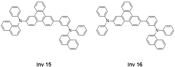


본 발명의 화학식 1로 표시되는 화합물은 일반적인 합성방법에 따라 합성될 수 있다 (Chem. Rev., 60:313 (1960); J. Chem. SOC. 4482 (1955); Chem. Rev. 95: 2457 (1995) 참조). 본 발명의 화합물에 대한 상세한 합성 과정은 후술하는 합성예에서 구체적으로 기술하도록 한다.
본 발명의 다른 측면은 상기한 본 발명에 따른 화학식 1로 표시되는 화합물을 포함하는 유기 전계 발광 소자에 관한 것이다.
구체적으로, 본 발명은 양극(anode); 음극(cathode); 및 상기 양극과 음극 사이에 개재(介在)된 1층 이상의 유기층을 포함하는 유기 EL 소자로서, 상기 1층 이상의 유기층 중 적어도 하나는 상기 화학식 1로 표시되는 화합물을 포함하는 것을 특징으로 한다.
상기 화학식 1의 화합물은 단독 또는 복수로 포함될 수 있다.
본 발명의 화학식 1로 표기되는 화합물을 포함하는 유기층은 정공주입층, 정공수송층, 전자수송층 및 발광층 중 어느 하나 이상일 수 있다. 바람직하게는, 상기 화학식 1로 표시되는 화합물은 정공 주입층, 정공 수송층 재료로서 유기 EL 소자에 포함될 수 있고, 이 경우 유기 EL 소자는 정공 저지 능력 및 정공 주입/수송 능력을 극대화할 수 있다. 또한 상기 화학식 1로 표시되는 화합물은 유기 EL 소자의 발광층 재료로 사용됨으로써, 향상된 효율을 제공할 수 있다.
본 발명에서 발광층은 인광 도판트 재료 또는 형광 도판트 재료를 포함할 수 있다. 바람직하게는, 본 발명의 화학식 1로 표기되는 화합물은 청색, 녹색, 및/또는 적색의 인광 호스트, 형광 호스트, 정공수송 물질, 정공주입 물질 및/또는 전자수송물질로서 유기 EL 소자에 포함될 수 있다.
또한 본 발명에 따른 화학식 1로 표시되는 화합물은 150℃ 이상의 높은 유리 전이 온도를 가지고 있다. 따라서 상기 화합물을 유기 EL 소자의 유기층으로 사용할 경우, 유기 EL 소자 내에서 결정화가 최소화되기 때문에 소자의 구동전압을 낮출 수 있고, 발광효율, 휘도, 열적 안정성 및 수명 특성을 개선할 수 있다.
본 발명에 따른 유기 EL 소자 구조의 비제한적인 예를 들면, 기판, 양극, 정공 주입층, 정공 수송층, 발광층, 전자 수송층 및 음극이 순차적으로 적층된 것일 수 있다. 이때 상기 발광층, 정공주입층, 정공수송층 및 전자수송층 중 하나 이상은 상기 화학식 1로 표시되는 화합물을 포함할 수 있다. 상기 전자 수송층 위에는 전자 주입층이 위치할 수도 있다.
또한, 본 발명에 따른 유기 EL 소자는 전술한 바와 같이 양극, 1층 이상의 유기층 및 음극이 순차적으로 적층된 구조뿐만 아니라, 전극과 유기층 계면에 절연층 또는 접착층이 삽입될 수도 있다.
본 발명의 유기 EL 소자에 있어서, 상기 화학식 1의 화합물을 포함하는 상기 유기층은 진공 증착이나 용액 도포에 의하여 형성될 수 있다. 상기 용액 도포의 예로는 스핀 코팅, 딥코팅, 닥터 블레이딩, 잉크젯 프린팅 또는 열 전사법 등이 있으나, 이들에만 한정되지 않는다.
본 발명의 유기 EL 소자는, 소자 내 유기층 중 1층 이상을 본 발명의 화학식 1로 표시되는 화합물을 포함하는 것을 제외하고는, 당 기술 분야에 알려져 있는 재료 및 방법을 이용하여 유기층 및 전극을 형성하여 제조될 수 있다.
예컨대, 기판으로는 실리콘 웨이퍼, 석영, 유리판, 금속판, 플라스틱 필름이나 시트 등이 사용될 수 있다.
양극 물질로는 바나듐, 크롬, 구리, 아연, 금과 같은 금속 또는 이들의 합금; 아연산화물, 인듐산화물, 인듐 주석 산화물 (ITO), 인듐 아연 산화물 (IZO)과 같은 금속 산화물; ZnO:Al 또는 SnO2:Sb와 같은 금속과 산화물의 조합물; 폴리티오펜, 폴리(3-메틸티오펜), 폴리[3,4-(에틸렌-1,2-디옥시)티오펜] (PEDT), 폴리피롤 및 폴리아닐린과 같은 전도성 고분자; 또는 카본블랙 등이 있으나, 이들에만 한정되는 것은 아니다.
음극 물질로는 마그네슘, 칼슘, 나트륨, 칼륨, 타이타늄, 인듐, 이트륨, 리튬, 가돌리늄, 알루미늄, 은, 주석 또는 납과 같은 금속 또는 이들의 합금; LiF/Al 또는 LiO2/Al과 같은 다층 구조 물질 등이 있으나, 이들에만 한정되는 것은 아니다.
상기 정공 주입층, 정공 수송층, 전자 수송층 및 전자 주입층은 특별히 한정되는 것은 아니며, 당 업계에 알려진 통상의 물질이 사용될 수 있다.
이하 본 발명을 실시예를 통하여 상세히 설명하면 다음과 같다. 단, 하기 실시예는 본 발명을 예시하는 것일 뿐 본 발명이 하기 실시예에 의해 한정되는 것은 아니다.
<준비예 1> triphenylene-2,7-diyl bis(trifluoromethanesulfonate)의 합성
<
단계 1> 화합물 1 (3,3'-dimethoxy-o-terphenyl)의 합성
[반응식 1]

1,2-dibromobenzene (50g, 214 mmol), 3-methoxyphenylboronic acid (65.1g, 428 mmol) 및 Pd(PPh3)4 (4.95g, 4.28 mmol)을 플라스크에 넣고 질소 분위기 하에 톨루엔 1.4 L 에 용해시킨 후 소듐 카보네이트 (118.2g, 856 mmol)을 녹인 수용액 1.2L을 첨가하여 12시간 동안 환류 교반하였다. 반응이 종결된 후 디클로로메탄 200 ml로 3회 추출 후 추출액을 과량의 마그네슘 설페이트 (Magnesium sulphate)로 건조, 여과하고 여액을 감압 농축하였다. 조산물을 실리카겔 컬럼 크로마토그래피 [n-Hexane: Dichloromethane = 4 : 1 (v:v)]로 정제하여 백색 고체의 화합물 15 (43.5 g, 수율 70 %)을 수득하였다.
GC-Mass (이론치: 290.13 g/mol, 측정치: 290 g/mol)
<단계 2> 화합물 2 (2,7-dimethoxytriphenylene)의 합성
[반응식 2]

상기 <단계 1>에서 얻어진 화합물1 (40g, 137 mmol)을 플라스크에 넣고 질소 분위기 하에, 디클로로메탄 1 L 에 용해시킨 다음 Iron (III) chloride (44.4 g, 274 mmol)을 넣고 상온에서 12시간 동안 교반하였다. 이후 2 당량의 iron(III) choloride를 추가로 첨가한 뒤 1시간 더 교반하고, 메틸알콜과 물을 1:1의 비율로 1L를 첨가하였다. 반응이 종결된 후, 유기층을 분리하여 과량의 마그네슘 설페이트로 건조 및 여과하고 여액을 감압 농축하였다. 조산물을 실리카겔 컬럼 크로마토그래피 [n-Hexane: Dichloromethane = 2 : 3 (v:v)]로 분리하여 31.6g 의 생성물을 얻고 이를 아세토니트릴 600 ml에 재결정하여 옅은 노란색 고체의 화합물2 (28g, 수율 70 %)을 수득하였다.
GC-Mass (이론치: 288.12 g/mol, 측정치: 288 g/mol),
<단계 3> 화합물3 (2,7-dihydroxytriphenylene)의 합성
[반응식 3]

상기 <단계 2>에서 얻어진 화합물2 (25g, 86 mmol) 및 피리딘 하이드로클로라이드 (pyridine hydrochloride) (100g, 86 mmol)을 플라스크에 넣고 질소 분위기 하에서 220℃에서 90분간 환류 교반하였다. 반응이 종결된 후, 조산물을 과량의 물로 세척하여 화합물3 (20g, 수율 88 %)을 수득하였다.
GC-Mass (이론치: 260.08 g/mol, 측정치: 260 g/mol),
<단계 4> 화합물4 (triphenylene-2,7-diyl bis(trifluoromethanesulfonate))의 합성
[반응식 4]

상기 <단계 3>에서 얻어진 화합물3 (20 g, 77 mmol)을 플라스크에 넣고 질소 분위기 하에서 pyridine 385 ml에 용해하여 0℃에서 교반하였다. 여기에 trifluoromethanesylfonyl anhydride (43.5 g, 154 mmol)를 천천히 한 방울씩 적가한 후 상온에서 12시간 동안 교반하였다. 반응이 종결된 후, 반응물을 감압 농축한 뒤 얻어진 고체를 플라스크에 넣고 메틸알콜 500 ml를 첨가하여 1시간 동안 교반 및 여과하여 백색 고체의 혼합물을 35g 얻었다. 조산물을 헥산/디클로로메탄으로 재결정하여 백색 고체의 화합물 4(28g, 수율: 68 %)을 수득하였다.
GC-Mass (이론치: 523.98 g/mol, 측정치: 524 g/mol),
1H-NMR (THF-d8, 500MHz) .(ppm) 7.72 ~ 7.75(m, 2H), 7.78 ~ 7.80(m, 2H), 8.77 ~ 8.79(m, 4H), 8.92 ~ 8.94(m, 2H)
[합성예 1] : 화합물 Inv 1의 제조
하기 반응식 5의 반응 경로를 거쳐 화합물 Inv 1을 합성하였다.
[반응식 5]

1) 단계 1 : 중간체 5의 합성
상기 <준비예 1>에서 얻어진 화합물 4 (10 g, 19 mmol), N-(4-(4,4,5,5-tetramethyl-1,3,2-dioxaborolan-2-yl)phenyl)-N-phenylbenzenamine (6.34 g, 17.1 mmol) 및 Pd(PPh3)4 (0.65 g, 0.57 mmol)을 플라스크에 넣고 질소 분위기 하에 톨루엔 100 mL에 용해시킨 후 포타슘 카보네이트 (Potassium carbonate) (5.25 g, 38 mmol)을 녹인 수용액 20 mL를 첨가하여 12시간 동안 환류 교반하였다. 물 50 ml를 첨가하여 반응을 종결 시킨 후, 디클로로메탄 30 ml로 3회 추출 후 추출액을 과량의 마그네슘 설페이트로 건조, 여과하고 여액을 감압 농축하였다. 조산물을 실리카겔 컬럼 크로마토그래피 [n-Hexane: Dichloromethane = 7 : 3 (v:v)]로 정제하여 백색 고체의 화합물 5 (8.2 g, 수율 70 %)을 수득하였다.
GC-Mass (이론치: 619.14 g/mol, 측정치: 619 g/mol)
2) 단계 2 : Inv 1 의 합성
상기 <단계 1>에서 얻은 화합물 5 (8 g, 12mmol), 디페닐아민 (2.6 g, 15 mmol) 및 Pd(OAc)2 (0.08 g, 0.36 mmol), BINAP(0.45 g, 0.72 mmol)과 포타슘 카보네이트 (3.31g, 24mmol)을 플라스크에 넣고 질소 분위기 하에서 톨루엔 80 mL 에 용해시킨 후 12시간 동안 환류 교반하였다. 반응이 종결된 뒤 물 50ml를 첨가하고, 디클로로메탄 30 ml로 3회 추출 후 추출액을 과량의 마그네슘 설페이트로 건조, 여과하고 여액을 감압 농축하였다. 조산물을 실리카겔 컬럼 크로마토그래피 [n-Hexane: Dichloromethane = 3 : 1 (v:v)]로 정제하여 백색 고체의 화합물 Inv 1 (5.2 g, 수율 68 %)을 수득하였다.
GC-Mass (이론치: 638.27 g/mol, 측정치: 638 g/mol),
1H-NMR (THF-d8, 500MHz) .(ppm) 6.46 ~ 6.52(m, 10H), 6.98 ~ 7.08(m, 13H), 7.32(s, 1H), 7.46(m, 2H), 7.82 ~ 7.88(m, 2H), 8.12 ~ 8.18 (m, 2H), 8.68(m, 1H), 8.93(m, 1H), 9.15(s, 1H)
[합성예 2] : 화합물 Inv 3 의 제조
하기 반응식 6의 반응 경로를 거쳐 화합물 Inv 3을 합성하였다.
[반응식 6]

1) 단계 1 : 중간체 6의 합성
상기 <준비예 1>에서 얻어진 화합물 4 (10 g, 19 mmol), N-(3-(4,4,5,5-tetramethyl-1,3,2-dioxaborolan-2-yl)phenyl)-N-phenylbenzenamine (6.34 g, 17.1 mmol) 및 Pd(PPh3)4 (0.65 g, 0.57 mmol)을 플라스크에 넣고 질소 분위기 하에 톨루엔 100 mL에 용해시킨 후 포타슘 카보네이트 (5.25 g, 38 mmol)을 녹인 수용액 20 mL를 첨가하여 12시간 동안 환류 교반하였다. 물 50 ml를 첨가하여 반응을 종결 시킨 후, 디클로로메탄 30 ml로 3회 추출 후 추출액을 과량의 마그네슘 설페이트로 건조, 여과하고 여액을 감압 농축하였다. 조산물을 실리카겔 컬럼 크로마토그래피 [n-Hexane: Dichloromethane = 7 : 3 (v:v)]로 정제하여 백색 고체의 화합물 6 (8.6 g, 수율 73 %)을 수득하였다.
GC-Mass (이론치: 619.14 g/mol, 측정치: 619 g/mol)
2) 단계 2 : Inv 3 의 합성
상기 <단계 1>에서 얻은 화합물 5 (8 g, 12mmol), 디페닐 아민 (2.6 g, 15 mmol) 및 Pd(OAc)2 (0.08 g, 0.36 mmol), BINAP (0.45 g, 0.72 mmol)과 포타슘 카보네이트 ( 3.31g, 24mmol)을 플라스크에 넣고 질소 분위기 하에 톨루엔 80 mL에 용해시킨 후 12시간 동안 환류 교반하였다. 반응이 종결된 후 물 50ml 를 첨가하고, 디클로로메탄 30 ml로 3회 추출 후 추출액을 과량의 마그네슘 설페이트로 건조, 여과하고 여액을 감압 농축하였다. 조산물을 실리카겔 컬럼 크로마토그래피 [n-Hexane: Dichloromethane = 3 : 1 (v:v)]로 정제하여 백색 고체의 화합물 Inv 3 (5.5 g, 수율 72 %)을 수득하였다.
GC-Mass (이론치: 638.27 g/mol, 측정치: 638 g/mol),
1H-NMR (THF-d8, 500MHz) .(ppm) 6.42 ~ 6.46(m, 9H), 6.68(m, 1H), 6.84(s, 1H), 6.98 ~ 7.08(m, 14H), 7.32(s, 1H), 7.82 ~ 7.88(m, 2H), 8.12 ~ 8.18 (m, 2H), 8.68(m, 1H), 8.93(m, 1H), 9.15(s, 1H)
[합성예 3] : 화합물 Inv 6 의 제조
하기 반응식 7의 반응 경로를 거쳐 화합물 Inv 6을 합성하였다.
[반응식 7]

1) 단계 1 : 중간체 7의 합성
상기 <준비예 1>에서 얻어진 화합물 4 (10 g, 19 mmol), N-(3-(4,4,5,5-tetramethyl-1,3,2-dioxaborolan-2-yl)phenyl)-N-bis(diphenyl)benzenamine (8.9 g, 17.1 mmol) 및 Pd(PPh3)4 (0.65 g, 0.57 mmol)을 플라스크에 넣고 질소 분위기 하에 톨루엔 100 mL에 용해시킨 후 포타슘 카보네이트 (5.25 g, 38 mmol)을 녹인 수용액 20 mL를 첨가하여 12시간 동안 환류 교반하였다. 물 50 ml를 첨가하여 반응을 종결 시킨 후, 디클로로메탄 30 ml로 3회 추출 후 추출액을 과량의 마그네슘 설페이트로 건조, 여과하고 여액을 감압 농축하였다. 조산물을 실리카겔 컬럼 크로마토그래피 [n-Hexane: Dichloromethane = 7 : 3 (v:v)]로 정제하여 백색 고체의 화합물 7 (8.2 g, 수율 56 %)을 수득하였다.
GC-Mass (이론치: 771.21 g/mol, 측정치: 771 g/mol)
2) 단계 2 : Inv 6 의 합성
상기 <단계 1>에서 얻은 화합물 6 (6.1 g, 8mmol), Bis(diphenyl)amine (3.1 g, 9.6mmol) 및 Pd(OAc)2 (0.05 g, 0.24 mmol), BINAP (0.3 g, 0.48 mmol)과 포타슘 카보네이트 (3.31 g, 24 mmol)을 플라스크에 넣고 질소 분위기 하에 톨루엔 60 mL에 용해시킨 후 12시간 동안 환류 교반하였다. 반응이 종결된 뒤 물 30 ml를 첨가 후, 디클로로메탄 20 ml로 3회 추출 후 추출액을 과량의 마그네슘 설페이트로 건조, 여과하고 여액을 감압 농축하였다. 조산물을 실리카겔 컬럼 크로마토그래피 [n-Hexane: Dichloromethane = 3 : 1 (v:v)]로 정제하여 백색 고체의 화합물 Inv 6 (4.9 g, 수율 65 %)을 수득하였다.
*GC-Mass (이론치: 942.40 g/mol, 측정치: 942 g/mol),
1H-NMR (THF-d8, 500MHz) .(ppm) 6.52(m, 10H), 7.08(m, 1H), 7.32(s, 1H), 7.46 ~ 7.48(m, 22H), 7.75(m, 8H), 7.82 ~ 7.88(m, 2H), 8.12 ~ 8.18(m, 2H), 8.68(m, 1H), 8.93(m, 1H), 9.15(s, 1H)
[합성예 4] : 화합물 Inv 30 의 제조
하기 반응식 8의 반응 경로를 거쳐 화합물 Inv 30을 합성 하였다.
[반응식 8]

1) 단계 1 : Inv 30의 합성
상기 <준비예 1>에서 얻어진 화합물 4 (10 g, 19 mmol), N-(3-(4,4,5,5-tetramethyl-1,3,2-dioxaborolan-2-yl)phenyl)-N-phenylbenzenamine (15.5 g, 41.8 mmol) 및 Pd(PPh3)4 (0.65 g, 0.57 mmol)을 플라스크에 넣고 질소 분위기 하에 톨루엔 100 mL 에 용해시킨 후 소듐 카보네이트 (6 g, 57 mmol)을 녹인 수용액 20 mL를 첨가하여 12시간 동안 환류 교반하였다. 물 50 ml를 첨가하여 반응을 종결시킨 후, 디클로로메탄 50 ml로 3회 추출 후 추출액을 과량의 마그네슘 설페이트로 건조, 여과하고 여액을 감압 농축하였다. 조산물을 실리카겔 컬럼 크로마토그래피 [n-Hexane: Dichloromethane = 4 : 1 (v:v)]로 정제하여 백색 고체의 화합물 7 (11.12 g, 수율 82 %)을 수득하였다.
GC-Mass (이론치: 714.30 g/mol, 측정치: 714 g/mol)
1H-NMR (THF-d8, 500MHz) .(ppm) 6.46(m, 8H), 6.68(m, 2H), 6.84(m, 2H), 6.98 ~ 7.07(m, 14H), 7.85(m, 2H), 8.07(m, 2H), 8.52 ~ 8.58(m, 4H), 8.74(m, 2H)
[합성예 5] : 화합물 Inv 33 의 제조
하기 반응식 9의 반응 경로를 거쳐 화합물 Inv 33을 합성하였다.
[반응식 9]

1) 단계 1 : 중간체 8의 합성
1,3,5-Tribromobenzene (37 g, 120 mmol), 디페닐아민 (18.3 g, 108 mmol) 및 Pd(OAc)2 (0.8 g, 3.6 mmol), BINAP (4.47 g, 7.2 mmol), Potassium carbonate (33.2 g, 240 mmol)를 플라스크에 넣고 질소 분위기 하에 톨루엔 1L에 용해시킨 후 12시간 동안 환류 교반하였다. 12시간 후 물 500ml를 넣어 반응을 종결한 후, 디클로로메탄 300 ml로 3회 추출 후 추출액을 과량의 마그네슘 설페이트로 건조, 여과하고 여액을 감압 농축하였다. 조산물을 실리카겔 컬럼 크로마토그래피 [n-Hexane: Dichloromethane = 4 : 1 (v:v)]로 정제하여 백색 고체의 화합물 8 (36.7 g, 수율 65 %)을 수득하였다.
GC-Mass (이론치: 490.10 g/mol, 측정치: 490 g/mol)
2) 단계 2 : 중간체 9 의 합성
상기 <단계 1>에서 얻은 화합물 8 (24.5g, 50 mmol), Bis(pinacolate)diboron (25.4 g, 100 mmol) 및 Pd(dppf)2Cl2 (1.7 g, 1.5 mmol), 포타슘 아세테이트 (14.5 g, 150 mmol)를 플라스크에 넣고 질소 분위기 하에 톨루엔 350 mL에 용해시킨 후 12시간 동안 환류 교반하였다. 물 200 ml를 첨가하여 반응을 종결한 뒤, 디클로로메탄 100 ml로 3회 추출 후 추출액을 과량의 마그네슘 설페이트로 건조, 여과하고 여액을 감압 농축하였다. 조산물을 실리카겔 컬럼 크로마토그래피 [n-Hexane: Dichloromethane = 3 : 1 (v:v)]로 정제하여 백색 고체의 화합물 Inv 6 (19.9 g, 수율 74 %)을 수득하였다.
GC-Mass (이론치: 538.28 g/mol, 측정치: 538 g/mol),
3) 단계 3 : 중간체 10 의 합성
상기 <단계 2>에서 얻은 화합물 9 (10g, 18mmol)와 상기 <준비예 1>에서 얻은 화합물 4 (10g, 19mmol) 및 Pd(PPh3)4 (0.65 g, 0.57 mmol)를 플라스크에 넣고 질소 분위기 하에 톨루엔 80 mL에 용해시킨 후 포타슘 카보네이트 (5 g, 36 mmol)을 녹인 수용액 20 mL를 첨가하여 12시간 동안 환류 교반하였다. 반응이 종결된 뒤 디클로로메탄 20 ml로 3회 추출하고, 추출액을 과량의 Magnesium sulphate로 건조, 여과하고 여액을 감압 농축하였다. 조산물을 실리카겔 컬럼 크로마토그래피 [n-Hexane: Dichloromethane = 3 : 1 (v:v)]로 정제하여 백색 고체의 화합물 10 (6.13 g, 수율 65 %)을 수득하였다.
GC-Mass (이론치: 786.22 g/mol, 측정치: 786 g/mol),
4) 단계 4 : Inv 33의 합성
상기 <단계 3>에서 얻은 화합물 10 (6g, 7.6 mmol), 디페닐아민 (1.5 g, 9.2mmol) 및 Pd(Oac)2 (0.05g, 0.22mmol), BINAP (0.273g, 0.44mmol)과 포타슘 카보네이트 (3.15g, 22.8mmol)을 플라스크에 넣고 질소 분위기 하에 톨루엔 50 mL에 용해시킨 후 12시간 동안 환류 교반하였다. 물 30 ml를 첨가하여 반응을 종결한 뒤, 디클로로메탄 20 ml로 3회 추출 후 추출액을 과량의 마그네슘 설페이트로 건조, 여과하고 여액을 감압 농축하였다. 조산물을 실리카겔 컬럼 크로마토그래피 [n-Hexane: Dichloromethane = 3 : 1 (v:v)]로 정제하여 백색 고체의 화합물 Inv 33 (4.5 g, 수율 75 %)을 수득하였다.
GC-Mass (이론치: 805.35 g/mol, 측정치: 805 g/mol),
1H-NMR (THF-d8, 500MHz) .(ppm) 5.62(m, 1H), 6.04(s, 2H), 6.46(m, 12H), 6.98 ~ 7.08(m, 19H), 7.32(s, 1H), 7.82 ~ 7.88(m, 2H), 8.04(m, 1H), 8.12 ~ 8.18(m, 2H), 8.68(m, 1H), 8.93(m, 1H), 9.15(s, 1H)
[합성예 6] : 화합물 Inv 44 의 제조
하기 반응식 10의 반응 경로를 거쳐 화합물 Inv 61을 합성하였다.
[반응식 10]

1) 단계 1 : 중간체 11의 합성
상기 <준비예 1>에서 얻어진 화합물 4 (10 g, 19 mmol)와 8-(4,4,5,5-tetramethyl-1,3,2-dioxaborolan-2-yl)-5-phenyl-5H-pyrido[4,3-b]indole (6.3g, 17.1 mmol) 및 Pd(PPh3)4 (0.416 g, 0.38 mmol)을 플라스크에 넣고 질소 분위기 하에 톨루엔 80 mL에 용해시킨 후 포타슘 카보네이트 (4.9 g, 38 mmol)을 녹인 수용액 20 mL를 첨가하여 12시간 동안 환류 교반하였다. 반응이 종결된 후 물 30 ml 첨가한 후 디클로로메탄 30 ml로 3회 추출하고, 추출액을 과량의 마그네슘 설페이트로 건조, 여과하고 여액을 감압 농축하였다. 조산물을 실리카겔 컬럼 크로마토그래피 [n-Hexane: Dichloromethane = 4 : 1 (v:v)]로 정제하여 백색 고체의 화합물 11 (5.19 g, 수율 70 %)을 수득하였다.
GC-Mass (이론치: 618.12 g/mol, 측정치: 618 g/mol)
2) 단계 2 : Inv 44 의 합성
상기 <단계 1>에서 얻은 화합물 11 (5 g, 8 mmol), 9H-carbazole (1.6 g, 9.6 mmol) 및 Pd(Oac)2 (0.053 g, 0.24 mmol), BINAP (0.298 g, 0.48 mmol)과 포타슘 카보네이트 (3.3 g, 24 mmol)을 플라스크에 넣고 질소 분위기 하에 톨루엔 60 mL에 용해시킨 후 12시간 동안 환류 교반하였다. 물 30 ml를 첨가하여 반응을 종결한 뒤, 디클로로메탄 30 ml로 3회 추출 후 추출액을 과량의 마그네슘 설페이트로 건조, 여과하고 여액을 감압 농축하였다. 조산물을 실리카겔 컬럼 크로마토그래피 [n-Hexane: Dichloromethane = 2 : 1 (v:v)]로 정제하여 백색 고체의 화합물 Inv 44 ( 3.9 g, 수율 77 %)을 수득하였다.
GC-Mass (이론치: 635.24 g/mol, 측정치: 635 g/mol),
1H-NMR (THF-d8, 500MHz) .(ppm) 7.08 ~ 7.20(m, 4H), 7.30 ~ 7.40(m, 10H), 7.77 ~ 7.88(m, 4H), 8.04 ~ 8.19(m, 5H), 8.55 ~ 8.59(m, 2H), 8.90 ~ 8,93(m, 2H), 9.15(s, 1H), 9.34(s, 1H)
[합성예 7] : 화합물 Inv 61 의 제조
하기 반응식 11의 반응 경로를 거쳐 화합물 Inv 61을 합성하였다.
[반응식 11]

1) 단계 1 : 중간체 12의 합성
상기 <준비예 1>에서 얻어진 화합물 4 (10 g, 19 mmol)와 dibenzofuran-1-boronic acid (3.62 g, 17.1 mmol) 및 Pd(PPh3)4 (0.416 g, 0.38 mmol)을 플라스크에 넣고 질소 분위기 하에 Toluene 80 mL 에 용해시킨 후 Potassium carbonate (4.9 g, 38 mmol) 을 녹인 수용액 20 mL 를 첨가하여 12시간 동안 환류 교반하였다. 반응이 종결된 후 물 40 ml 첨가하고 디클로로메탄 30 ml로 3회 추출하고, 추출액을 과량의 마그네슘 설페이트로 건조, 여과하고 여액을 감압 농축하였다. 조산물을 실리카겔 컬럼 크로마토그래피 [n-Hexane: Dichloromethane = 2 : 1 (v:v)]로 정제하여 백색 고체의 화합물 12 (3.25 g, 수율 50 %)을 수득하였다.
GC-Mass (이론치: 542.08 g/mol, 측정치: 542 g/mol)
2) 단계 2 : Inv 61 의 합성
상기 <단계 1>에서 얻은 화합물 12 (3 g, 5.5 mmol), 디페닐아민 (1.12 g, 6.6 mmol) 및 Pd(Oac)2 (0.037g, 0.17 mmol), BINAP (0.225 g, 0.34mmol)과 포타슘 카보네이트 (2.27 g, 16.5mmol)을 플라스크에 넣고 질소 분위기 하에 톨루엔 50 mL에 용해시킨 후 12시간 동안 환류 교반하였다. 반응이 종결된 뒤 실리카겔 필터 후 걸러진 여액을 감압 농축하였다. 조산물을 실리카겔 컬럼 크로마토그래피 [n-Hexane: Dichloromethane = 2 : 1 (v:v)]로 정제하여 백색 고체의 화합물 Inv 61 (3.85 g, 수율 80 %)을 수득하였다.
GC-Mass (이론치: 561.21 g/mol, 측정치: 561 g/mol),
1H-NMR (THF-d8, 500MHz) .(ppm) 6.46(m, 4H), 6.98 ~ 7.08(m, 7H), 7.19(m, 1H), 7.31 ~ 7.39(m, 3H), 7.54(m, 1H), 7.82 ~ 8.04(m, 6H), 8.12 ~ 8.18(m, 2H), 8.68(m, 1H), 8.93(m, 1H), 9.15(s, 1H)
[합성예 8] : 화합물 Inv 63 의 제조
하기 반응식 12의 반응 경로를 거쳐 화합물 Inv 63을 합성하였다.
[반응식 12]

1) 단계 1 : 중간체 13의 합성
상기 <준비예 1>에서 얻어진 화합물 4 (10 g, 19 mmol)와 dibenzothiophene-4-boronic acid (3.89 g, 17.1 mmol) 및 Pd(PPh3)4 (0.416 g, 0.38 mmol)을 플라스크에 넣고 질소 분위기 하에 톨루엔 80 mL 에 용해시킨 후 포타슘 카보네이트 (4.9 g, 38 mmol) 을 녹인 수용액 20 mL를 첨가하여 12시간 동안 환류 교반하였다. 반응이 종결된 후 물 40 ml 첨가 후 디클로로메탄 30 ml로 3회 추출 하고, 추출액을 과량의 마그네슘 설페이트로 건조, 여과하고 여액을 감압 농축하였다. 조산물을 실리카겔 컬럼 크로마토그래피 [n-Hexane: Dichloromethane = 2 : 1 (v:v)]로 정제하여 백색 고체의 화합물 13 (5.2 g, 수율 78 %)을 수득하였다.
GC-Mass (이론치: 558.06 g/mol, 측정치: 558 g/mol)
2) 단계 2 : Inv 63 의 합성
상기 <단계 1>에서 얻은 화합물 13 (3.06g, 5.5 mmol), 디페닐 아민 (1.12 g, 6.6 mmol) 및 Pd(Oac)2 (0.037g, 0.17 mmol), BINAP (0.225 g, 0.34mmol)과 포타슘 카보네이트 (2.27 g, 16.5mmol)을 플라스크에 넣고 질소 분위기 하에 톨루엔 50 mL에 용해시킨 후 12시간 동안 환류 교반하였다. 반응이 종결된 뒤, 실리카겔 필터 후 걸러진 여액을 감압 농축하였다. 조산물을 실리카겔 컬럼 크로마토그래피 [n-Hexane: Dichloromethane = 2 : 1 (v:v)]로 정제하여 백색 고체의 화합물 Inv 63 (2.6 g, 수율 85 %)을 수득하였다.
GC-Mass (이론치: 577.19 g/mol, 측정치: 577 g/mol),
1H-NMR (THF-d8, 500MHz) .(ppm) 6.46(m, 4H), 6.98 ~ 7.08(m, 7H), 7.32 ~ 7.39(m, 2H), 7.49 ~ 7.56(m, 3H), 7.82 ~ 7.88(m, 3H), 8.04(m, 1H), 8.12 ~ 8.20(m, 3H), 8.41 ~ 8.45(m, 2H), 8.68(m, 1H), 8.93(m, 1H), 9.15(s, 1H)
<실시예 1 ~14> 유기 EL 소자의 제조
ITO (Indium tin oxide)가 1500 두께로 박막 코팅된 유리 기판을 증류수 초음파로 세척하였다. 증류수 세척이 끝나면 이소프로필 알코올, 아세톤, 메탄올 등의 용제로 초음파 세척을 하고 건조시킨 후, UV OZONE 세정기 (Power sonic 405, 화신테크)로 이송시킨 다음 UV를 이용하여 상기 기판을 5 분간 세정한 후 진공 층착기로 기판을 이송하였다.
상기와 같이 준비된 ITO 투명 전극 위에 전공 수송층 재료로써, m-MTDATA(60nm)/합성예 1~5에서 합성된 각각의 화합물 (80nm)/DS-H522 + 5% DS-501(300nm)/BCP(10nm)/Alq3(30 nm)/LiF(1nm)/Al(200nm) 순서로 유기 EL 소자를 제조하였다. 또한 인광 호스트 성능 측정을 위해서, m-MTDATA(60nm)/TCTA/합성예 6~8에서 합성된 각각의 화합물 + 10% Ir(ppy)3 (300nm)/BCP(10nm)/Alq3(30 nm)/LiF(1nm)/Al(200nm) 순으로 유기 EL 소자를 제조하였다.
소자 제작에 사용된 DS-H522 와 DS-501 은 ㈜ 두산 전자 BG 제품이며, m-MTDATA, TCTA, CBP, Ir(ppy)3, 및 BCP의 구조는 아래와 같다.


<비교예 1> 유기 EL 소자의 제조
정공 수송층 형성시 합성예에서 제조된 화합물 대신 상기 NPB를 발광호스트 물질로 사용한 것을 제외하고는, 상기 실시예 1과 동일한 방법으로 유기 EL 소자를 제조하였다.
<비교예 2> 유기 EL 소자의 제조
발광층 형성시 합성예에서 제조된 화합물 대신 상기 CBP를 발광호스트 물질로 사용한 것을 제외하고는, 상기 실시예 1과 동일한 방법으로 유기 EL 소자를 제조하였다.
<실험예 1> 유기 전계 발광소자의 성능 평가
실시예 1~8 및 비교예 1~2에서 제조된 각 유기 EL 소자에 대하여 구동전압, 전류효율, 발광 피크에서의 휘도를 각각 측정하고, 그 결과를 하기 표 1에 나타내었다.
표 1
| 소자 | HTL | 전압(V) | 휘도(cd/m2) | EL peak(nm) | 전류효율(cd/A) |
| 비교예 1 | NPB | 5.2 | 1816 | 521 | 18.1 |
| 실시예 1 | Inv 1 | 4.7 | 2363 | 522 | 23.6 |
| 실시예 2 | Inv 3 | 4.9 | 2273 | 519 | 22.7 |
| 실시예 3 | Inv 6 | 4.8 | 2205 | 522 | 22.1 |
| 실시예 4 | Inv 30 | 5.1 | 2120 | 521 | 21.2 |
| 실시예 5 | Inv 33 | 5.2 | 2015 | 521 | 20.2 |
상기 표 1의 결과로부터 알 수 있는 바와 같이, 본 발명에 따른 트리페닐렌계화합물을 녹색 유기 EL 소자의 정공 수송층으로 사용하는 실시예 1~5의 경우 종래 NPB를 사용한 청색 유기 EL 소자(비교예 1)와 대비하여 볼 때, 효율 및 전압 면에서 향상된 성능을 나타내었다. 또한 유리 전이 온도 (Tg) 값의 향상을 통하여 수명의 개선 효과 또한 기대해 볼 수 있다.
표 2
| 소자 | HOST | 전압(V) | 휘도(cd/m2) | EL peak(nm) | 전류효율(cd/A) |
| 비교예 2 | CBP | 6.93 | 445 | 516 | 38.2 |
| 실시예 6 | Inv 44 | 6.12 | 430 | 518 | 39.5 |
| 실시예 7 | Inv 61 | 6.82 | 455 | 520 | 40.4 |
| 실시예 8 | Inv 63 | 6.45 | 479 | 520 | 44.6 |
마찬가지로, 본 발명에 따른 화합물을 인광 발광성 녹색 유기 EL 소자의 발광층으로 사용하는 실시예 6~8의 경우, 종래의 CBP를 사용한 녹색 유기 EL 소자(비교예 2)와 대비하여 발광 효율 및 구동 전압 면에서 향상된 성능을 나타내는 것을 확인할 수 있다 (표 2 참조).
이상을 통해 본 발명의 바람직한 실시예에 대하여 설명하였지만, 본 발명은 이에 한정되는 것이 아니고 특허청구범위와 발명의 상세한 설명의 범위 안에서 여러 가지로 변형하여 실시하는 것이 가능하고 이 또한 본 발명의 범위에 속하는 것은 당연하다.
본 발명에 따른 상기 화학식 1의 화합물은 유기 EL 소자용 재료로 사용되어 종래에 정공 주입 및 수송 물질로 사용되던 사용되는 NPB 에 비해 높은 정공 주입 및 수송 능력을 통하여 전력 효율 개선 및 발광 효율 향상을 발휘할 수 있다.
또한, 인광 호스트 재료로 사용되던 4,4-dicarbazolybiphenyl (CBP)에 비해 저전력, 고효율, 고휘도 및 향상된 내구성과 수명을 확보할 수 있다.
Claims (7)
- 하기 화학식 1로 표시되는 화합물:[화학식 1]
 상기 식에서,A는 단일결합, 페닐, 나프틸, 치환 또는 비치환된 핵원자수 6 내지 10의 헤테로 아릴이며, 이때 상기 헤테로 아릴에 도입되는 치환기는 할로겐 원자, 탄소수 1~3의 알킬기 및 탄소수 6 내지 10의 아릴기로 구성된 군으로부터 선택되며;B는 치환 또는 비치환된 C6 내지 C10 사이의 아릴, 치환 또는 비치환된 핵원자수 6 내지 10의 헤테로 아릴이며, 이때 상기 아릴 또는 헤테로 아릴에 도입되는 치환기는 할로겐 원자, 탄소수 1~3의 알킬기 및 탄소수 6 내지 10의 아릴기로 구성된 군으로부터 선택되며;이때 A 와 B는 각각 독립적으로 동일하거나 상이할 수 있으며,X 는 N, O, S 중 하나이며,l, m 은 각각 독립적으로 0 또는 1이며, 이때 X가 O 또는 S인 경우 l과 m 중 하나는 0이며,n은 1 또는 2 의 정수이며,Ar1 내지 Ar4는 치환 또는 비치환된 C6 내지 C20의 아릴, 치환 또는 비치환된 핵원자수 5 내지 20의 헤테로 아릴이며, 이때 아릴, 헤테로 아릴에 도입되는 치환기는 중수소 또는 할로겐 원자, 탄소수 1~3의 알킬기, 탄소수 6 내지 10의 아릴기로 구성된 군으로부터 선택되며, 이들은 각각 독립적으로 동일하거나 상이할 수 있다.
 - 제 1 항에 있어서, 상기 화학식 1로 표시되는 화합물은 하기 화학식 2 내지 4로 표시되는 것이 특징인 화합물:[화학식 2]
 [화학식 3]
 [화학식 4]
 상기 화학식 2 내지 4에서,A, B, n, Ar1 내지 Ar4는 각각 제1항에 정의된 바와 같다.
 - 제 1 항에 있어서, 상기 화학식 1 중 A 또는 B가 핵원자수 6 내지 10의 헤테로 아릴인 경우 하기 화학식 5로 표기되는 치환기 군으로부터 선택되는 것을 특징으로 하는 화합물:[화학식 5]
 상기 화학식 5의 치환기 군에 도입되는 복수 개의 Z 는 각각 독립적이며, 동일하게 표기되더라도 동일하거나 서로 상이할 수 있으며, 복수 개의 Z 중 적어도 1개 이상은 질소원자이며, 나머지는 탄소원자이다.
 - 제 1 항에 있어서, 상기 화학식 1 중 Ar1과 Ar2는 A 또는 인접하는 치환기와 서로 결합하여 축합환을 형성할 수 있으며,Ar3와 Ar4는 B 또는 인접하는 치환기와 결합하여 축합환을 형성할 수 있는 것을 특징으로 하는 화합물.
- 양극; 음극; 및 상기 양극과 음극 사이에 개재(介在)된 1층 이상의 유기층을 포함하는 유기 전계발광 소자로서,상기 유기층 중 적어도 하나는 제 1 항 내지 제 4 항 중 어느 한 항에 기재된 화합물을 포함하는 것을 특징으로 하는 유기 전계발광 소자.
- 제 5 항에 있어서, 상기 유기층은 발광층, 전자수송층, 정공 주입층 및 정공 수송층으로 구성된 군으로부터 선택되는 것을 특징으로 하는 유기 전계발광 소자.
- 제 5 항에 있어서, 상기 화합물은 발광층, 전자수송층, 정공 주입층 또는 정공 수송층 물질인 것을 특징으로 하는 유기 전계발광 소자.
Applications Claiming Priority (2)
| Application Number | Priority Date | Filing Date | Title |
|---|---|---|---|
| KR1020100042665A KR101218029B1 (ko) | 2010-05-06 | 2010-05-06 | 방향족 아민을 포함하는 트리페닐렌계 화합물 및 이를 포함하는 유기 전계 발광 소자 |
| KR10-2010-0042665 | 2010-05-06 |
Publications (2)
| Publication Number | Publication Date |
|---|---|
| WO2011139129A2 true WO2011139129A2 (ko) | 2011-11-10 |
| WO2011139129A3 WO2011139129A3 (ko) | 2012-04-19 |
Family
ID=44904254
Family Applications (1)
| Application Number | Title | Priority Date | Filing Date |
|---|---|---|---|
| PCT/KR2011/003416 Ceased WO2011139129A2 (ko) | 2010-05-06 | 2011-05-06 | 방향족 아민을 포함하는 트리페닐렌계 화합물 및 이를 포함하는 유기 전계 발광 소자 |
Country Status (2)
| Country | Link |
|---|---|
| KR (1) | KR101218029B1 (ko) |
| WO (1) | WO2011139129A2 (ko) |
Cited By (10)
| Publication number | Priority date | Publication date | Assignee | Title |
|---|---|---|---|---|
| WO2012176674A1 (ja) * | 2011-06-23 | 2012-12-27 | 東レ株式会社 | 発光素子 |
| JP2014001327A (ja) * | 2012-06-20 | 2014-01-09 | Sumitomo Chemical Co Ltd | 高分子化合物およびそれを用いた発光素子 |
| JP2014509306A (ja) * | 2010-12-29 | 2014-04-17 | エルジー・ケム・リミテッド | 新規な化合物およびこれを用いた有機発光素子 |
| US20150034924A1 (en) * | 2011-10-24 | 2015-02-05 | Hodogaya Chemical Co., Ltd. | Novel triphenylene derivatives and organic electroluminescent devices using said derivatives |
| EP2924753A1 (en) * | 2014-03-25 | 2015-09-30 | Novaled GmbH | Polychromatic light emitting devices and versatile hole transporting matrix for them |
| CN105073718A (zh) * | 2013-05-16 | 2015-11-18 | 第一毛织株式会社 | 有机化合物、有机光电元件及显示元件 |
| US20160028014A1 (en) * | 2014-07-22 | 2016-01-28 | Samsung Display Co., Ltd. | Organic light-emitting device |
| JP2016526029A (ja) * | 2013-05-16 | 2016-09-01 | チェイル インダストリーズ インコーポレイテッド | 有機化合物、有機光電子素子および表示装置 |
| WO2017069258A1 (ja) * | 2015-10-21 | 2017-04-27 | 出光興産株式会社 | 新規化合物、有機エレクトロルミネッセンス素子用材料、有機エレクトロルミネッセンス素子及び電子機器 |
| CN113214174A (zh) * | 2014-05-27 | 2021-08-06 | 环球展览公司 | 有机电致发光材料及其用途 |
Families Citing this family (4)
| Publication number | Priority date | Publication date | Assignee | Title |
|---|---|---|---|---|
| KR20140135525A (ko) | 2013-05-16 | 2014-11-26 | 제일모직주식회사 | 유기 광전자 소자용 발광 재료, 유기 광전자 소자 및 표시 장치 |
| KR101433822B1 (ko) * | 2013-06-17 | 2014-08-27 | 삼성디스플레이 주식회사 | 유기 발광 장치 |
| KR101627761B1 (ko) | 2013-07-10 | 2016-06-07 | 제일모직 주식회사 | 유기 화합물, 유기 광전자 소자 및 표시 장치 |
| KR102227046B1 (ko) * | 2018-06-14 | 2021-03-12 | 주식회사 엘지화학 | 화합물 및 이를 포함하는 유기 발광 소자 |
Family Cites Families (4)
| Publication number | Priority date | Publication date | Assignee | Title |
|---|---|---|---|---|
| JP2006143845A (ja) * | 2004-11-18 | 2006-06-08 | Konica Minolta Holdings Inc | 有機エレクトロルミネッセンス素子用材料、有機エレクトロルミネッセンス素子、照明装置及び表示装置 |
| KR100753454B1 (ko) * | 2006-02-03 | 2007-08-31 | 주식회사 이엘엠 | 고성능 유기 발광 재료 및 유기 발광 다이오드 |
| JP5669580B2 (ja) * | 2007-09-20 | 2015-02-12 | ビーエーエスエフ ソシエタス・ヨーロピアBasf Se | エレクトロルミネセンスデバイス |
| JP5353069B2 (ja) * | 2008-06-04 | 2013-11-27 | 三菱化学株式会社 | トリフェニレン系化合物、トリフェニレン系化合物を含有する有機電界発光素子及び有機elディスプレイ |
-
2010
- 2010-05-06 KR KR1020100042665A patent/KR101218029B1/ko active Active
-
2011
- 2011-05-06 WO PCT/KR2011/003416 patent/WO2011139129A2/ko not_active Ceased
Cited By (16)
| Publication number | Priority date | Publication date | Assignee | Title |
|---|---|---|---|---|
| JP2014509306A (ja) * | 2010-12-29 | 2014-04-17 | エルジー・ケム・リミテッド | 新規な化合物およびこれを用いた有機発光素子 |
| US8946695B2 (en) | 2010-12-29 | 2015-02-03 | Lg Chem, Ltd. | Compound, and organic light-emitting device using same |
| WO2012176674A1 (ja) * | 2011-06-23 | 2012-12-27 | 東レ株式会社 | 発光素子 |
| US20150034924A1 (en) * | 2011-10-24 | 2015-02-05 | Hodogaya Chemical Co., Ltd. | Novel triphenylene derivatives and organic electroluminescent devices using said derivatives |
| JP2014001327A (ja) * | 2012-06-20 | 2014-01-09 | Sumitomo Chemical Co Ltd | 高分子化合物およびそれを用いた発光素子 |
| US9735369B2 (en) | 2013-05-16 | 2017-08-15 | Cheil Industries, Inc. | Luminescent material for organic optoelectric device and organic optoelectric device and display device |
| CN105073718A (zh) * | 2013-05-16 | 2015-11-18 | 第一毛织株式会社 | 有机化合物、有机光电元件及显示元件 |
| JP2016526029A (ja) * | 2013-05-16 | 2016-09-01 | チェイル インダストリーズ インコーポレイテッド | 有機化合物、有機光電子素子および表示装置 |
| CN105073718B (zh) * | 2013-05-16 | 2018-03-09 | 第一毛织株式会社 | 有机化合物、有机光电元件及显示元件 |
| WO2015144633A1 (en) * | 2014-03-25 | 2015-10-01 | Novaled Gmbh | Polychromatic light emitting devices and versatile hole transporting matrix for them |
| CN106414394A (zh) * | 2014-03-25 | 2017-02-15 | 诺瓦尔德股份有限公司 | 多色发光器件及其通用空穴传输基质 |
| EP2924753A1 (en) * | 2014-03-25 | 2015-09-30 | Novaled GmbH | Polychromatic light emitting devices and versatile hole transporting matrix for them |
| CN106414394B (zh) * | 2014-03-25 | 2018-11-23 | 诺瓦尔德股份有限公司 | 多色发光器件及其通用空穴传输基质 |
| CN113214174A (zh) * | 2014-05-27 | 2021-08-06 | 环球展览公司 | 有机电致发光材料及其用途 |
| US20160028014A1 (en) * | 2014-07-22 | 2016-01-28 | Samsung Display Co., Ltd. | Organic light-emitting device |
| WO2017069258A1 (ja) * | 2015-10-21 | 2017-04-27 | 出光興産株式会社 | 新規化合物、有機エレクトロルミネッセンス素子用材料、有機エレクトロルミネッセンス素子及び電子機器 |
Also Published As
| Publication number | Publication date |
|---|---|
| KR20110123172A (ko) | 2011-11-14 |
| KR101218029B1 (ko) | 2013-01-02 |
| WO2011139129A3 (ko) | 2012-04-19 |
Similar Documents
| Publication | Publication Date | Title |
|---|---|---|
| WO2011139129A2 (ko) | 방향족 아민을 포함하는 트리페닐렌계 화합물 및 이를 포함하는 유기 전계 발광 소자 | |
| WO2020027389A1 (ko) | 유기발광 화합물 및 이를 포함하는 유기발광소자 | |
| WO2014010823A1 (ko) | 헤테로환 화합물 및 이를 포함하는 유기 전자 소자 | |
| WO2013009079A1 (ko) | 트리페닐렌계 화합물 및 이를 이용한 유기 전계 발광 소자 | |
| WO2011139125A2 (ko) | 페난스로카바졸 화합물 및 이를 이용한 유기 전계 발광 소자 | |
| WO2013002509A2 (ko) | 새로운 화합물 및 이를 이용한 유기 발광 소자 | |
| WO2011149240A2 (ko) | 바이폴라 트리페닐렌계 화합물 및 이를 포함하는 유기 전계 발광 소자 | |
| WO2012099376A2 (ko) | 신규한 화합물 및 이를 포함하는 유기 발광 소자 | |
| WO2011081431A2 (ko) | 유기발광 화합물 및 이를 포함한 유기 전계 발광 소자 | |
| WO2011059271A2 (ko) | 신규한 축합고리 화합물 및 이를 이용한 유기전자소자 | |
| WO2020040514A1 (ko) | 유기 발광 소자 | |
| WO2019164301A1 (ko) | 화합물 및 이를 포함하는 유기 발광 소자 | |
| WO2020111733A1 (ko) | 유기 발광 소자 | |
| WO2019045405A1 (ko) | 헤테로고리 화합물 및 이를 이용한 유기 발광 소자 | |
| WO2014098455A1 (ko) | 신규 유기 화합물 및 이를 포함하는 유기 전계 발광 소자 | |
| WO2017061779A1 (ko) | 아민 화합물 및 이를 포함하는 유기 발광 소자 | |
| WO2017061832A1 (ko) | 신규 화합물 및 이를 포함하는 유기 발광 소자 | |
| WO2019013526A1 (ko) | 신규한 화합물 및 이를 포함하는 유기 발광 소자 | |
| WO2020009492A9 (ko) | 다환 화합물 및 이를 포함하는 유기 발광 소자 | |
| WO2010058946A2 (ko) | 신규한 크라이센 유도체 및 이를 이용한 유기 전기 소자 | |
| WO2014123391A1 (ko) | 헤테로환 화합물 및 이를 이용한 유기 발광 소자 | |
| WO2020111586A1 (ko) | 신규한 화합물 및 이를 이용한 유기 발광 소자 | |
| WO2019160315A1 (ko) | 헤테로고리 화합물 및 이를 포함하는 유기 발광 소자 | |
| WO2011081449A2 (ko) | 트리페닐렌계 화합물 및 이를 포함하는 유기 전계 발광 소자 | |
| WO2024112021A1 (ko) | 신규한 화합물 및 이를 포함한 유기 발광 소자 |
Legal Events
| Date | Code | Title | Description |
|---|---|---|---|
| 121 | Ep: the epo has been informed by wipo that ep was designated in this application |
Ref document number: 11777610 Country of ref document: EP Kind code of ref document: A2 |
|
| NENP | Non-entry into the national phase |
Ref country code: DE |
|
| 32PN | Ep: public notification in the ep bulletin as address of the adressee cannot be established |
Free format text: NOTING OF LOSS OF RIGHTS PURSUANT TO RULE 112(1) EPC (EPO FORM 1205A DATED 18.02.2013) |
|
| 122 | Ep: pct application non-entry in european phase |
Ref document number: 11777610 Country of ref document: EP Kind code of ref document: A2 |