WO2011126135A1 - Ledモジュール - Google Patents
Ledモジュール Download PDFInfo
- Publication number
- WO2011126135A1 WO2011126135A1 PCT/JP2011/059014 JP2011059014W WO2011126135A1 WO 2011126135 A1 WO2011126135 A1 WO 2011126135A1 JP 2011059014 W JP2011059014 W JP 2011059014W WO 2011126135 A1 WO2011126135 A1 WO 2011126135A1
- Authority
- WO
- WIPO (PCT)
- Prior art keywords
- led
- led module
- pad
- module according
- pads
- Prior art date
- Legal status (The legal status is an assumption and is not a legal conclusion. Google has not performed a legal analysis and makes no representation as to the accuracy of the status listed.)
- Ceased
Links
Images










Classifications
-
- H—ELECTRICITY
- H10—SEMICONDUCTOR DEVICES; ELECTRIC SOLID-STATE DEVICES NOT OTHERWISE PROVIDED FOR
- H10H—INORGANIC LIGHT-EMITTING SEMICONDUCTOR DEVICES HAVING POTENTIAL BARRIERS
- H10H20/00—Individual inorganic light-emitting semiconductor devices having potential barriers, e.g. light-emitting diodes [LED]
- H10H20/80—Constructional details
- H10H20/85—Packages
- H10H20/855—Optical field-shaping means, e.g. lenses
- H10H20/856—Reflecting means
-
- H—ELECTRICITY
- H10—SEMICONDUCTOR DEVICES; ELECTRIC SOLID-STATE DEVICES NOT OTHERWISE PROVIDED FOR
- H10H—INORGANIC LIGHT-EMITTING SEMICONDUCTOR DEVICES HAVING POTENTIAL BARRIERS
- H10H20/00—Individual inorganic light-emitting semiconductor devices having potential barriers, e.g. light-emitting diodes [LED]
- H10H20/80—Constructional details
- H10H20/85—Packages
- H10H20/857—Interconnections, e.g. lead-frames, bond wires or solder balls
-
- H—ELECTRICITY
- H10—SEMICONDUCTOR DEVICES; ELECTRIC SOLID-STATE DEVICES NOT OTHERWISE PROVIDED FOR
- H10W—GENERIC PACKAGES, INTERCONNECTIONS, CONNECTORS OR OTHER CONSTRUCTIONAL DETAILS OF DEVICES COVERED BY CLASS H10
- H10W90/00—Package configurations
-
- H—ELECTRICITY
- H10—SEMICONDUCTOR DEVICES; ELECTRIC SOLID-STATE DEVICES NOT OTHERWISE PROVIDED FOR
- H10H—INORGANIC LIGHT-EMITTING SEMICONDUCTOR DEVICES HAVING POTENTIAL BARRIERS
- H10H20/00—Individual inorganic light-emitting semiconductor devices having potential barriers, e.g. light-emitting diodes [LED]
- H10H20/80—Constructional details
- H10H20/85—Packages
- H10H20/8506—Containers
-
- H—ELECTRICITY
- H10—SEMICONDUCTOR DEVICES; ELECTRIC SOLID-STATE DEVICES NOT OTHERWISE PROVIDED FOR
- H10W—GENERIC PACKAGES, INTERCONNECTIONS, CONNECTORS OR OTHER CONSTRUCTIONAL DETAILS OF DEVICES COVERED BY CLASS H10
- H10W72/00—Interconnections or connectors in packages
- H10W72/071—Connecting or disconnecting
- H10W72/075—Connecting or disconnecting of bond wires
- H10W72/07551—Connecting or disconnecting of bond wires characterised by changes in properties of the bond wires during the connecting
- H10W72/07554—Connecting or disconnecting of bond wires characterised by changes in properties of the bond wires during the connecting changes in dispositions
-
- H—ELECTRICITY
- H10—SEMICONDUCTOR DEVICES; ELECTRIC SOLID-STATE DEVICES NOT OTHERWISE PROVIDED FOR
- H10W—GENERIC PACKAGES, INTERCONNECTIONS, CONNECTORS OR OTHER CONSTRUCTIONAL DETAILS OF DEVICES COVERED BY CLASS H10
- H10W72/00—Interconnections or connectors in packages
- H10W72/50—Bond wires
- H10W72/531—Shapes of wire connectors
- H10W72/536—Shapes of wire connectors the connected ends being ball-shaped
-
- H—ELECTRICITY
- H10—SEMICONDUCTOR DEVICES; ELECTRIC SOLID-STATE DEVICES NOT OTHERWISE PROVIDED FOR
- H10W—GENERIC PACKAGES, INTERCONNECTIONS, CONNECTORS OR OTHER CONSTRUCTIONAL DETAILS OF DEVICES COVERED BY CLASS H10
- H10W72/00—Interconnections or connectors in packages
- H10W72/50—Bond wires
- H10W72/531—Shapes of wire connectors
- H10W72/5363—Shapes of wire connectors the connected ends being wedge-shaped
-
- H—ELECTRICITY
- H10—SEMICONDUCTOR DEVICES; ELECTRIC SOLID-STATE DEVICES NOT OTHERWISE PROVIDED FOR
- H10W—GENERIC PACKAGES, INTERCONNECTIONS, CONNECTORS OR OTHER CONSTRUCTIONAL DETAILS OF DEVICES COVERED BY CLASS H10
- H10W72/00—Interconnections or connectors in packages
- H10W72/50—Bond wires
- H10W72/541—Dispositions of bond wires
- H10W72/547—Dispositions of multiple bond wires
-
- H—ELECTRICITY
- H10—SEMICONDUCTOR DEVICES; ELECTRIC SOLID-STATE DEVICES NOT OTHERWISE PROVIDED FOR
- H10W—GENERIC PACKAGES, INTERCONNECTIONS, CONNECTORS OR OTHER CONSTRUCTIONAL DETAILS OF DEVICES COVERED BY CLASS H10
- H10W72/00—Interconnections or connectors in packages
- H10W72/50—Bond wires
- H10W72/541—Dispositions of bond wires
- H10W72/547—Dispositions of multiple bond wires
- H10W72/5473—Dispositions of multiple bond wires multiple bond wires connected to a common bond pad
-
- H—ELECTRICITY
- H10—SEMICONDUCTOR DEVICES; ELECTRIC SOLID-STATE DEVICES NOT OTHERWISE PROVIDED FOR
- H10W—GENERIC PACKAGES, INTERCONNECTIONS, CONNECTORS OR OTHER CONSTRUCTIONAL DETAILS OF DEVICES COVERED BY CLASS H10
- H10W72/00—Interconnections or connectors in packages
- H10W72/851—Dispositions of multiple connectors or interconnections
- H10W72/874—On different surfaces
- H10W72/884—Die-attach connectors and bond wires
-
- H—ELECTRICITY
- H10—SEMICONDUCTOR DEVICES; ELECTRIC SOLID-STATE DEVICES NOT OTHERWISE PROVIDED FOR
- H10W—GENERIC PACKAGES, INTERCONNECTIONS, CONNECTORS OR OTHER CONSTRUCTIONAL DETAILS OF DEVICES COVERED BY CLASS H10
- H10W90/00—Package configurations
- H10W90/701—Package configurations characterised by the relative positions of pads or connectors relative to package parts
- H10W90/731—Package configurations characterised by the relative positions of pads or connectors relative to package parts of die-attach connectors
- H10W90/734—Package configurations characterised by the relative positions of pads or connectors relative to package parts of die-attach connectors between a chip and a stacked insulating package substrate, interposer or RDL
-
- H—ELECTRICITY
- H10—SEMICONDUCTOR DEVICES; ELECTRIC SOLID-STATE DEVICES NOT OTHERWISE PROVIDED FOR
- H10W—GENERIC PACKAGES, INTERCONNECTIONS, CONNECTORS OR OTHER CONSTRUCTIONAL DETAILS OF DEVICES COVERED BY CLASS H10
- H10W90/00—Package configurations
- H10W90/701—Package configurations characterised by the relative positions of pads or connectors relative to package parts
- H10W90/751—Package configurations characterised by the relative positions of pads or connectors relative to package parts of bond wires
- H10W90/754—Package configurations characterised by the relative positions of pads or connectors relative to package parts of bond wires between a chip and a stacked insulating package substrate, interposer or RDL
Definitions
- the present invention relates to an LED module including an LED chip as a light source.
- FIG. 19 shows an example of a conventional LED module (for example, Patent Document 1).
- the LED module X shown in the figure includes a case 91, a submount substrate 92, a wiring pattern 93, an LED chip 94, and a light transmitting part 95.
- Case 91 is made of resin, for example.
- the submount substrate 92 is made of Si, for example.
- the wiring pattern 93 is formed on the submount substrate 92, and its surface is made of, for example, Au or Ag.
- the LED chip 94 is a light source of the LED module X that emits light of a predetermined wavelength.
- the LED chip 94 is mounted on the submount substrate 92 by eutectic bonding to the wiring pattern 93.
- the light transmitting part 95 is made of, for example, a silicone resin that can transmit light from the LED chip 94 and covers the LED chip 94.
- the present invention has been conceived under the circumstances described above, and an object of the present invention is to provide an LED module capable of suppressing a decrease in light amount due to secular change.
- An LED module provided by the first aspect of the present invention includes a case having an LED unit including one or more LED chips, a main body made of ceramics, and one or more pads for mounting the LED unit.
- the pad has an outer edge located inside the outer edge of the LED unit in plan view.
- the surface of the pad is made of Ag or Au.
- the main body is white.
- the LED module provided by any one of the first to third aspects of the present invention comprises one or more wires having one end bonded to the LED unit.
- the case further includes one or more bonding pads, to which the other end of the wire is bonded, and located outside the pad in plan view.
- the main body is formed with a reflector surrounding the LED unit.
- the reflector is formed with a recess that accommodates at least a part of the bonding pad in plan view.
- the case in the LED module provided by any one of the first to fifth aspects of the present invention, includes one or more mountings provided on the side opposite to the pad. It further has an electrode and a through conductor portion that penetrates the main body and connects any of the pads and any of the mounting electrodes.
- the LED unit consists only of the LED chip.
- the LED unit further includes a submount substrate on which the LED chip is mounted. To do.
- the plurality of pads arranged in a plurality of rows and mounted on the plurality of pads.
- the LED unit and the pad are eutectic bonded.
- a resin that covers the LED unit and transmits light from the LED unit includes a light-transmitting portion made of a material and a fluorescent material that emits light having a wavelength different from that of the light from the LED unit when excited by the light from the LED unit.
- FIG. 2 is a cross-sectional view taken along the line II-II in FIG.
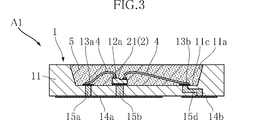
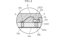
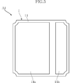
- FIG. 3 is a sectional view taken along line III-III in FIG. 1. It is a principal part expanded sectional view which shows the LED module based on 1st Embodiment of this invention. It is a bottom view which shows the LED module based on 1st Embodiment of this invention. It is a top view which shows the LED module based on 2nd Embodiment of this invention.
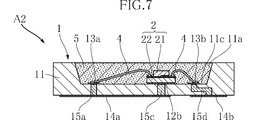
- FIG. 7 is a cross-sectional view taken along line VII-VII in FIG. 6.
- FIG. 7 is a sectional view taken along line VIII-VIII in FIG. 6.
- FIG. 15 is a sectional view taken along line XV-XV in FIG. 14. It is sectional drawing which follows the XVI-XVI line
- the LED module A1 of the present embodiment includes a case 1, a plurality of LED units 2, a Zener diode 3, a wire 4, and a light transmitting portion 5 (omitted in FIG. 1).
- the LED module A1 is a high-power LED module with relatively high brightness, and has a planar view size of about 5 mm square and a thickness of about 0.9 mm.
- Case 1 includes a main body 11, a plurality of pads 12a and 12b, a plurality of bonding pads 13a and 13b, a pad 16, a pair of mounting electrodes 14a and 14b, and a plurality of through conductor portions 15a, 15b, 15c, and 15d.
- Case 1 is made of white ceramics such as alumina, for example.
- a reflector 11a and a bottom surface 11c are formed in the main body 11.
- the reflector 11a reflects light that has traveled in the left-right direction in FIG. 2 from the plurality of LED chips 21 so as to be directed upward in the drawing.
- four recesses 11b are formed in the reflector 11a.
- the four recesses 11b have a substantially triangular cross-sectional shape in plan view and reach the bottom surface 11c.
- the bottom surface 11c has a substantially circular shape, and is connected to the lower end edge of the reflector 11a.
- the plurality of pads 12a and 12b are formed on the bottom surface 11c, and in the present embodiment, three pads 12a and three pads 12b are arranged in two rows.
- 12a and 12b have a rectangular shape, and are formed of plating layers laminated in the order of, for example, Ag / Ni / Au or Ag / Ni / Ag, or W / Ni / Ag or W / Ni / Au from the bottom surface 11c side.
- the surface layer is made of Ag
- the thickness of the Ag layer is about 2.5 ⁇ m.
- the thickness of the Au layer is about 0.1 ⁇ m.
- the plurality of bonding pads 13a and 13b are formed on the bottom surface 11c, and in this embodiment, three bonding pads 13a and three bonding pads 13b are arranged in two rows.
- the bonding pads 13a and 13b are rectangular and have the same plating structure as the pads 12a and 12b.
- the bonding pads 13a and 13b located at the four corners of the bonding pads 13a and 13b are configured such that about 1/3 of the respective portions are accommodated in the four recesses 11b.
- the pad 16 is disposed relatively near the edge of the bottom surface 11 c and has a plating structure similar to that of the pad 12 and the bonding pad 13.
- the pair of mounting electrodes 14 a and 14 b are formed on the surface of the main body 11 opposite to the side on which the reflector 11 a and the bottom surface 11 c are formed.
- the mounting electrode 14a is significantly larger than the mounting electrode 14b, and overlaps the plurality of LED chips 21 in plan view.
- the plurality of through conductor portions 15a, 15b, 15c, and 15d penetrate the main body 11, and are made of, for example, Ag or W.
- the three through conductor portions 15a connect the three bonding pads 13a and the mounting electrodes 14a.
- the three through conductor portions 15b connect the three pads 12a and the mounting electrode 14a.
- the three through conductor portions 15c connect the three pads 12b and the mounting electrode 14a.
- One through conductor portion 15c connects the pad 16 and the mounting electrode 14a.
- the three through conductor portions 15d connect the three bonding pads 13b and the mounting electrodes 14b, and are formed in a crank shape.
- the case 1 having such a structure can be formed by firing a laminate in which ceramic material and Ag material or W material are appropriately laminated in order, and plating the resultant.
- the plurality of LED units 2 are light sources of the LED module A1, and are composed of a plurality of LED chips 21 in this embodiment.
- Each LED chip 21 has, for example, an n-type semiconductor layer made of a GaN-based semiconductor, a p-type semiconductor layer, and an active layer sandwiched between them, and emits blue light.
- Each LED chip 21 is eutectic bonded to the pads 12a and 12b.
- the planar view dimensions of each LED chip 21 are larger than the planar view dimensions of the pads 12a and 12b. That is, as shown in FIG. 4, the outer edge 121a in the plan view of the pad 12a is located slightly inside the outer edge 2a of the LED unit 2 (LED chip 21). The same applies to the outer edge of the pad 12b.
- the LED chip 21 is configured as a so-called 2-wire type LED chip.
- the Zener diode 3 is for preventing an excessive reverse voltage from being applied to the plurality of LED chips 21, and has a function of allowing a reverse current to pass only when an excessive reverse voltage exceeding a certain voltage is applied. Fulfill. Zener diode 3 is bonded to pad 16 via, for example, Ag paste.
- the plurality of wires 4 are made of, for example, Au, one end of which is bonded to the bonding pads 13a and 13b, and the other end is bonded to the LED chip 21 or the Zener diode 3.
- the translucent part 5 is filled in a region surrounded by the reflector 11a and the bottom surface 11c, and covers the plurality of LED chips 21, the Zener diode 3, and the plurality of wires 4.
- the translucent part 5 is made of a material in which a phosphor substance is mixed in a transparent silicone resin, for example.
- the phosphor material emits yellow light when excited by, for example, blue light from the LED chip 21. When the yellow light and the blue light from the LED chip 21 are mixed, white light is emitted from the LED module A1.
- a phosphor material that emits red light when excited by blue light and a phosphor material that emits green light may be used.
- the pads 12a and 12b are hidden by the LED chip 21. For this reason, even if the pads 12a and 12b become dark black due to aging with use, the light from the LED chip 21 toward the bottom surface 11c is not absorbed by the pads 12a and 12b but is reflected by the bottom surface 11c. . Therefore, it is possible to suppress a decrease in the amount of light due to aging of the LED module A1, and it is possible to increase the brightness of the LED module A1.
- the bonding pads 13 a and 13 b are not completely hidden by the LED chip 21 or the wire 4, the bonding pads 13 a and 13 b are arranged outside the LED chip 21 and separated from the LED chip 21. Thereby, it can suppress that the light from LED chip 21 is absorbed by bonding pad 13a, 13b.
- the reflector 11a can be made relatively close to the LED chip 21. This is suitable for increasing the brightness of the LED module A1. Further, the main body 11 made of ceramics can transmit light from the LED chip 21 to some extent. Making the reflector 11a relatively closer to the LED chip 21 contributes to increasing the portion outside the reflector 11a without changing the external dimensions of the main body 11. Thereby, it can avoid that the light from LED chip 21 permeate
- the through conductor portions 15b and 15c do not perform an electrical function, but perform a function of transmitting heat generated from the LED chip 21 from the pads 12a and 12b to the mounting electrode 14a. Thereby, the heat dissipation of the LED chip 21 can be enhanced, and the input current to the LED chip 21 can be increased. This is advantageous for increasing the brightness of the LED module A1.
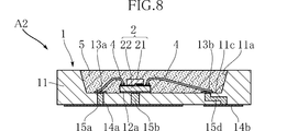
- the LED module A2 of the present embodiment is different from the above-described embodiment in the configuration of the LED unit 2.
- the LED unit 2 includes an LED chip 21 and a submount substrate 22.
- the submount substrate 22 is made of, for example, Si, and the LED chip 21 is mounted thereon.
- a wiring pattern is formed on the submount substrate 22. This wiring pattern has a portion that is electrically connected to an electrode (not shown) of the LED chip 21 and extends to a region that is not covered by the LED 21. In the present embodiment, the wire 4 is bonded to this wiring pattern.
- the submount substrate 22 is bonded to the pads 12a and 12b by Ag paste 17, for example. This bonding may be performed by eutectic bonding.
- the plan view dimensions of the pads 12a and 12b are smaller than the plan view dimensions of the submount substrate 22.
- the outer edge 121a of the pad 12a in plan view is the LED unit 2 (submount substrate 22). ) Is located slightly inside the outer edge 2a. The same applies to the outer edge of the pad 12b.
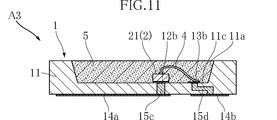
- the LED module A3 of the present embodiment is different from any of the above-described embodiments in the configuration of the LED unit 2.
- the LED unit 2 includes only the LED chip 21 and is configured as a so-called one-wire type LED unit. Further, the bonding pads 13a and the through conductor portions 15a provided in the case 1 in the LED modules A1 and A2 are not provided in connection with the LED unit 2 being a one-wire type.
- electrodes are formed on the upper and lower surfaces of the LED chip 21.
- a wire 4 is bonded to the electrode formed on the upper surface.
- the electrodes formed on the lower surface are bonded to the pads 12a and 12b by eutectic bonding, for example.
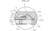
- the planar view dimensions of the pads 12a and 12b are smaller than the planar view dimensions of the LED chip 21, and the outer edge 121b in the plan view of the pad 12b is formed on the LED unit 2 (LED chip 21) as shown in FIG. It is located slightly inside the outer edge 2a.
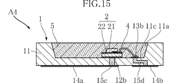
- the LED module A4 of the present embodiment is different from the above-described embodiment in the configuration of the LED unit 2.
- the LED unit 2 includes an LED chip 21 and a submount substrate 22 and is configured as a so-called one-wire type LED unit.
- the submount substrate 22 is made of, for example, Si, and the LED chip 21 is mounted thereon.
- a wiring pattern is formed on the submount substrate 22 via an insulating film. This wiring pattern has a portion that is electrically connected to an electrode (not shown) of the LED chip 21 and extends to a region that is not covered by the LED 21. In the present embodiment, the wire 4 is bonded to this wiring pattern.
- the submount substrate 22 is made a conductive body by, for example, a doping process.
- the other electrode (not shown) of the LED chip 21 is in contact with the submount substrate 22 and is conductive.
- the submount substrate 22 is bonded to the pads 12a and 12b by Ag paste 17, for example. This bonding may be performed by eutectic bonding.
- the plan view dimensions of the pads 12a and 12b are smaller than the plan view dimensions of the submount substrate 22.
- the outer edge 121b in the plan view of the pad 12b is an LED. It is located slightly inside the outer edge 2a of the unit 2 (submount substrate 22).
- FIG. 18 shows an LED module based on the fifth embodiment of the present invention.
- the LED module A5 of this embodiment has the same configuration as the LED module A1 described above except that the configurations of the through conductor portions 15a, 15b, 15c, and 15d are different.
- the penetration conductor part 15b is not illustrated, it is the structure similar to the penetration conductor part 15c.
- the through conductor portion 15c is provided at a position retracted from the LED unit 2 (LED chip 21) in plan view.
- the pad 12b and the through conductor portion 15c are electrically connected by a plating layer extending from the pad 12b.
- the through conductor portions 15a and 15d are provided at positions retracted from the bonded portion of the wire in plan view.
- the LED module according to the present invention is not limited to the embodiment described above.
- the specific configuration of each part of the LED module according to the present invention can be changed in various ways.
- the plurality of LED chips 21 may emit light having different wavelengths.
- the shape of the bottom surface 11c is not limited to a circle.
- the translucent part 5 may be formed only with a transparent material.
Landscapes
- Led Device Packages (AREA)
Abstract
Description
Claims (11)
- 1以上のLEDチップを具備するLEDユニットと、
セラミックスからなる本体、および上記LEDユニットを搭載するための1以上のパッド、を有するケースと、を備えており、
上記パッドは、平面視においてその外縁が上記LEDユニットの外縁よりも内側に位置する、LEDモジュール。 - 上記パッドの表面は、AgまたはAuからなる、請求項1に記載のLEDモジュール。
- 上記本体は、白色である、請求項1に記載のLEDモジュール。
- 上記LEDユニットにボンディングされた一端を有する1以上のワイヤを備えており、
上記ケースは、上記ワイヤの他端がボンディングされ、かつ上記パッドよりも平面視において外側に位置する、1以上のボンディングパッドをさらに有する、請求項1に記載のLEDモジュール。 - 上記本体には、上記LEDユニットを囲むリフレクタが形成されており、
上記リフレクタには、平面視において上記ボンディングパッドの少なくとも一部を収容する凹部が形成されている、請求項1に記載のLEDモジュール。 - 上記ケースは、上記パッドとは反対側に設けられた1以上の実装電極と、上記本体を貫通し、かつ上記パッドのいずれかと上記実装電極のいずれかとを接続する貫通導体部と、をさらに有する、請求項1に記載のLEDモジュール。
- 上記LEDユニットは、上記LEDチップのみからなる、請求項1に記載の、LEDモジュール。
- 上記LEDユニットは、上記LEDチップが搭載されたサブマウント基板をさらに具備する、請求項1に記載の、LEDモジュール。
- 複数列に配置された複数の上記パッドと、
複数の上記パッドに搭載された複数の上記LEDユニットと、を備える、請求項1に記載のLEDモジュール。 - 上記LEDユニットと上記パッドとは、共晶接合されている、請求項1に記載のLEDモジュール。
- 上記LEDユニットを覆い、かつ、上記LEDユニットからの光を透過する樹脂材料と、上記LEDユニットからの光によって励起されることにより上記LEDユニットからの光とは異なる波長の光を発する蛍光材料と、からなる透光部をさらに備える、請求項1に記載のLEDモジュール。
Priority Applications (5)
| Application Number | Priority Date | Filing Date | Title |
|---|---|---|---|
| CN201180018197.6A CN102834942B (zh) | 2010-04-09 | 2011-04-11 | Led模块 |
| US13/638,248 US9722157B2 (en) | 2010-04-09 | 2011-04-11 | LED module |
| JP2012509720A JP5939977B2 (ja) | 2010-04-09 | 2011-04-11 | Ledモジュール |
| US15/634,602 US20170294567A1 (en) | 2010-04-09 | 2017-06-27 | Led module |
| US16/556,896 US11605765B2 (en) | 2010-04-09 | 2019-08-30 | LED module |
Applications Claiming Priority (2)
| Application Number | Priority Date | Filing Date | Title |
|---|---|---|---|
| JP2010-090712 | 2010-04-09 | ||
| JP2010090712 | 2010-04-09 |
Related Child Applications (2)
| Application Number | Title | Priority Date | Filing Date |
|---|---|---|---|
| US13/638,248 A-371-Of-International US9722157B2 (en) | 2010-04-09 | 2011-04-11 | LED module |
| US15/634,602 Continuation US20170294567A1 (en) | 2010-04-09 | 2017-06-27 | Led module |
Publications (1)
| Publication Number | Publication Date |
|---|---|
| WO2011126135A1 true WO2011126135A1 (ja) | 2011-10-13 |
Family
ID=44763070
Family Applications (1)
| Application Number | Title | Priority Date | Filing Date |
|---|---|---|---|
| PCT/JP2011/059014 Ceased WO2011126135A1 (ja) | 2010-04-09 | 2011-04-11 | Ledモジュール |
Country Status (4)
| Country | Link |
|---|---|
| US (3) | US9722157B2 (ja) |
| JP (1) | JP5939977B2 (ja) |
| CN (2) | CN105720180B (ja) |
| WO (1) | WO2011126135A1 (ja) |
Cited By (1)
| Publication number | Priority date | Publication date | Assignee | Title |
|---|---|---|---|---|
| JP2018032748A (ja) * | 2016-08-24 | 2018-03-01 | パナソニックIpマネジメント株式会社 | 発光装置、照明装置及び発光装置の製造方法 |
Families Citing this family (4)
| Publication number | Priority date | Publication date | Assignee | Title |
|---|---|---|---|---|
| JP6034175B2 (ja) * | 2012-01-10 | 2016-11-30 | ローム株式会社 | Ledモジュール |
| JP5963001B2 (ja) * | 2013-03-28 | 2016-08-03 | 東芝ライテック株式会社 | 照明装置 |
| TWI767246B (zh) | 2014-12-30 | 2022-06-11 | 荷蘭商露明控股公司 | 具有用於氣體或液體冷卻之集成特徵之發光二極體封裝 |
| US20190237629A1 (en) * | 2018-01-26 | 2019-08-01 | Lumileds Llc | Optically transparent adhesion layer to connect noble metals to oxides |
Citations (6)
| Publication number | Priority date | Publication date | Assignee | Title |
|---|---|---|---|---|
| JP2003264267A (ja) * | 2002-03-08 | 2003-09-19 | Rohm Co Ltd | 半導体チップを使用した半導体装置 |
| JP2006286944A (ja) * | 2005-03-31 | 2006-10-19 | Dowa Mining Co Ltd | サブマウント及びその製造方法 |
| JP2006324392A (ja) * | 2005-05-18 | 2006-11-30 | Kyocera Corp | 発光素子搭載用基板,発光素子収納用パッケージ,発光装置および照明装置 |
| JP2007258420A (ja) * | 2006-03-23 | 2007-10-04 | Rohm Co Ltd | Led発光装置およびその製造方法 |
| JP2008047834A (ja) * | 2006-08-21 | 2008-02-28 | Hamamatsu Photonics Kk | 半導体装置および半導体装置製造方法 |
| JP2008270327A (ja) * | 2007-04-17 | 2008-11-06 | Matsushita Electric Ind Co Ltd | 静電気対策部品およびこれを用いた発光ダイオードモジュール |
Family Cites Families (34)
| Publication number | Priority date | Publication date | Assignee | Title |
|---|---|---|---|---|
| JPH07199829A (ja) | 1993-12-28 | 1995-08-04 | Harrison Denki Kk | 発光ユニットおよび表示装置ならびに照明装置 |
| US6294407B1 (en) * | 1998-05-06 | 2001-09-25 | Virtual Integration, Inc. | Microelectronic packages including thin film decal and dielectric adhesive layer having conductive vias therein, and methods of fabricating the same |
| US6667541B1 (en) * | 1998-10-21 | 2003-12-23 | Matsushita Electric Industrial Co., Ltd. | Terminal land frame and method for manufacturing the same |
| US7242033B2 (en) | 2002-03-08 | 2007-07-10 | Rohm Co., Ltd. | Semiconductor device using LED chip |
| US7244965B2 (en) * | 2002-09-04 | 2007-07-17 | Cree Inc, | Power surface mount light emitting die package |
| CN102290409B (zh) * | 2003-04-01 | 2014-01-15 | 夏普株式会社 | 发光装置 |
| JP2005167174A (ja) * | 2003-11-14 | 2005-06-23 | Harison Toshiba Lighting Corp | 発光素子の外囲器 |
| KR100586944B1 (ko) * | 2003-12-26 | 2006-06-07 | 삼성전기주식회사 | 고출력 발광다이오드 패키지 및 제조방법 |
| JP2005252219A (ja) * | 2004-02-06 | 2005-09-15 | Toyoda Gosei Co Ltd | 発光装置及び封止部材 |
| JP5094118B2 (ja) * | 2004-08-03 | 2012-12-12 | 株式会社トクヤマ | 発光素子収納用パッケージおよび発光素子収納用パッケージの製造方法 |
| JP4659421B2 (ja) * | 2004-09-30 | 2011-03-30 | 株式会社トクヤマ | 発光素子収納用パッケージの製造方法 |
| US7473933B2 (en) * | 2004-10-29 | 2009-01-06 | Ledengin, Inc. (Cayman) | High power LED package with universal bonding pads and interconnect arrangement |
| JP4601404B2 (ja) | 2004-11-26 | 2010-12-22 | 京セラ株式会社 | 発光装置および照明装置 |
| KR100587017B1 (ko) * | 2005-02-23 | 2006-06-08 | 삼성전기주식회사 | 발광 다이오드 패키지 및 그 제조 방법 |
| JP2006237141A (ja) | 2005-02-23 | 2006-09-07 | Stanley Electric Co Ltd | サブマウント型led |
| JP2006261569A (ja) * | 2005-03-18 | 2006-09-28 | Dowa Mining Co Ltd | サブマウントおよびその製造方法 |
| TWI514522B (zh) | 2005-03-18 | 2015-12-21 | 同和電子科技有限公司 | 副載置片及其製造方法 |
| JP2006324317A (ja) * | 2005-05-17 | 2006-11-30 | Kyoritsu Elex Co Ltd | 発光ダイオード及び発光ダイオード用パッケージ |
| KR101241650B1 (ko) * | 2005-10-19 | 2013-03-08 | 엘지이노텍 주식회사 | 엘이디 패키지 |
| US7399658B2 (en) * | 2005-10-21 | 2008-07-15 | Stats Chippac Ltd. | Pre-molded leadframe and method therefor |
| US8310060B1 (en) * | 2006-04-28 | 2012-11-13 | Utac Thai Limited | Lead frame land grid array |
| TWI321857B (en) * | 2006-07-21 | 2010-03-11 | Epistar Corp | A light emitting device |
| JP5205724B2 (ja) | 2006-08-04 | 2013-06-05 | 日亜化学工業株式会社 | 発光装置 |
| US20100224890A1 (en) * | 2006-09-18 | 2010-09-09 | Cree, Inc. | Light emitting diode chip with electrical insulation element |
| WO2008038708A1 (en) * | 2006-09-29 | 2008-04-03 | Rohm Co., Ltd. | Semiconductor light emitting device |
| US20080225449A1 (en) | 2007-03-13 | 2008-09-18 | Tatsuya Inoue | Electrostatic discharge protection component, and electronic component module using the same |
| JP2008251936A (ja) * | 2007-03-30 | 2008-10-16 | Rohm Co Ltd | 半導体発光装置 |
| US8421093B2 (en) * | 2007-07-13 | 2013-04-16 | Rohm Co., Ltd. | LED module and LED dot matrix display |
| TWI528508B (zh) * | 2008-10-13 | 2016-04-01 | 榮創能源科技股份有限公司 | 高功率發光二極體陶瓷封裝之製造方法 |
| JP5363789B2 (ja) * | 2008-11-18 | 2013-12-11 | スタンレー電気株式会社 | 光半導体装置 |
| KR101018153B1 (ko) * | 2008-11-27 | 2011-02-28 | 삼성엘이디 주식회사 | Led 패키지 |
| KR101018191B1 (ko) * | 2008-11-27 | 2011-02-28 | 삼성엘이디 주식회사 | 세라믹 패키지 및 이를 구비하는 헤드램프 모듈 |
| JP5585013B2 (ja) * | 2009-07-14 | 2014-09-10 | 日亜化学工業株式会社 | 発光装置 |
| JP5640632B2 (ja) * | 2010-03-12 | 2014-12-17 | 旭硝子株式会社 | 発光装置 |
-
2011
- 2011-04-11 US US13/638,248 patent/US9722157B2/en active Active
- 2011-04-11 WO PCT/JP2011/059014 patent/WO2011126135A1/ja not_active Ceased
- 2011-04-11 CN CN201610143740.XA patent/CN105720180B/zh active Active
- 2011-04-11 CN CN201180018197.6A patent/CN102834942B/zh active Active
- 2011-04-11 JP JP2012509720A patent/JP5939977B2/ja active Active
-
2017
- 2017-06-27 US US15/634,602 patent/US20170294567A1/en not_active Abandoned
-
2019
- 2019-08-30 US US16/556,896 patent/US11605765B2/en active Active
Patent Citations (6)
| Publication number | Priority date | Publication date | Assignee | Title |
|---|---|---|---|---|
| JP2003264267A (ja) * | 2002-03-08 | 2003-09-19 | Rohm Co Ltd | 半導体チップを使用した半導体装置 |
| JP2006286944A (ja) * | 2005-03-31 | 2006-10-19 | Dowa Mining Co Ltd | サブマウント及びその製造方法 |
| JP2006324392A (ja) * | 2005-05-18 | 2006-11-30 | Kyocera Corp | 発光素子搭載用基板,発光素子収納用パッケージ,発光装置および照明装置 |
| JP2007258420A (ja) * | 2006-03-23 | 2007-10-04 | Rohm Co Ltd | Led発光装置およびその製造方法 |
| JP2008047834A (ja) * | 2006-08-21 | 2008-02-28 | Hamamatsu Photonics Kk | 半導体装置および半導体装置製造方法 |
| JP2008270327A (ja) * | 2007-04-17 | 2008-11-06 | Matsushita Electric Ind Co Ltd | 静電気対策部品およびこれを用いた発光ダイオードモジュール |
Cited By (1)
| Publication number | Priority date | Publication date | Assignee | Title |
|---|---|---|---|---|
| JP2018032748A (ja) * | 2016-08-24 | 2018-03-01 | パナソニックIpマネジメント株式会社 | 発光装置、照明装置及び発光装置の製造方法 |
Also Published As
| Publication number | Publication date |
|---|---|
| US20130020605A1 (en) | 2013-01-24 |
| CN105720180B (zh) | 2018-05-29 |
| US20190386190A1 (en) | 2019-12-19 |
| JP5939977B2 (ja) | 2016-06-29 |
| US20170294567A1 (en) | 2017-10-12 |
| CN102834942A (zh) | 2012-12-19 |
| US9722157B2 (en) | 2017-08-01 |
| US11605765B2 (en) | 2023-03-14 |
| CN102834942B (zh) | 2016-04-13 |
| CN105720180A (zh) | 2016-06-29 |
| JPWO2011126135A1 (ja) | 2013-07-11 |
Similar Documents
| Publication | Publication Date | Title |
|---|---|---|
| JP5768435B2 (ja) | 発光装置 | |
| TWI636589B (zh) | 發光二極體模組及其製作方法 | |
| JP4881358B2 (ja) | 発光装置 | |
| EP2673812B1 (en) | Light emitting device having wavelength converting layer | |
| JP6131048B2 (ja) | Ledモジュール | |
| JP5133120B2 (ja) | 発光装置 | |
| US11605765B2 (en) | LED module | |
| JP2010245481A (ja) | 発光装置 | |
| JP2008244165A (ja) | 照明装置 | |
| JP2013140823A (ja) | 発光装置 | |
| WO2013150882A1 (ja) | Led発光装置 | |
| JP2008251664A (ja) | 照明装置 | |
| JPWO2014050650A1 (ja) | 発光装置 | |
| JP2005340494A (ja) | 発光ダイオードランプ | |
| KR102397909B1 (ko) | 기판 및 이를 포함하는 광원 모듈 | |
| JP2008078401A (ja) | 照明装置 | |
| JP5809440B2 (ja) | Ledモジュール | |
| TWI420713B (zh) | 發光二極體封裝結構及其製造方法 | |
| JP2022181403A (ja) | 発光装置 | |
| CN205920987U (zh) | 发光二极管封装件 | |
| KR20110131429A (ko) | 발광소자 및 이의 제조방법 | |
| KR101806790B1 (ko) | 반도체 발광소자 | |
| KR101806789B1 (ko) | 반도체 발광소자 | |
| JP5320374B2 (ja) | 発光装置の製造方法 | |
| KR101772551B1 (ko) | 반도체 발광 구조물 및 이의 제조방법 |
Legal Events
| Date | Code | Title | Description |
|---|---|---|---|
| WWE | Wipo information: entry into national phase |
Ref document number: 201180018197.6 Country of ref document: CN |
|
| 121 | Ep: the epo has been informed by wipo that ep was designated in this application |
Ref document number: 11766035 Country of ref document: EP Kind code of ref document: A1 |
|
| WWE | Wipo information: entry into national phase |
Ref document number: 13638248 Country of ref document: US |
|
| WWE | Wipo information: entry into national phase |
Ref document number: 2012509720 Country of ref document: JP |
|
| NENP | Non-entry into the national phase |
Ref country code: DE |
|
| 122 | Ep: pct application non-entry in european phase |
Ref document number: 11766035 Country of ref document: EP Kind code of ref document: A1 |