WO2011125527A1 - 光電変換素子、その製造方法、光センサ、及び撮像素子 - Google Patents
光電変換素子、その製造方法、光センサ、及び撮像素子 Download PDFInfo
- Publication number
- WO2011125527A1 WO2011125527A1 PCT/JP2011/057251 JP2011057251W WO2011125527A1 WO 2011125527 A1 WO2011125527 A1 WO 2011125527A1 JP 2011057251 W JP2011057251 W JP 2011057251W WO 2011125527 A1 WO2011125527 A1 WO 2011125527A1
- Authority
- WO
- WIPO (PCT)
- Prior art keywords
- photoelectric conversion
- layer
- group
- conversion element
- ring
- Prior art date
- Legal status (The legal status is an assumption and is not a legal conclusion. Google has not performed a legal analysis and makes no representation as to the accuracy of the status listed.)
- Ceased
Links
Images

Classifications
-
- H—ELECTRICITY
- H10—SEMICONDUCTOR DEVICES; ELECTRIC SOLID-STATE DEVICES NOT OTHERWISE PROVIDED FOR
- H10F—INORGANIC SEMICONDUCTOR DEVICES SENSITIVE TO INFRARED RADIATION, LIGHT, ELECTROMAGNETIC RADIATION OF SHORTER WAVELENGTH OR CORPUSCULAR RADIATION
- H10F39/00—Integrated devices, or assemblies of multiple devices, comprising at least one element covered by group H10F30/00, e.g. radiation detectors comprising photodiode arrays
- H10F39/10—Integrated devices
- H10F39/12—Image sensors
-
- H—ELECTRICITY
- H10—SEMICONDUCTOR DEVICES; ELECTRIC SOLID-STATE DEVICES NOT OTHERWISE PROVIDED FOR
- H10F—INORGANIC SEMICONDUCTOR DEVICES SENSITIVE TO INFRARED RADIATION, LIGHT, ELECTROMAGNETIC RADIATION OF SHORTER WAVELENGTH OR CORPUSCULAR RADIATION
- H10F39/00—Integrated devices, or assemblies of multiple devices, comprising at least one element covered by group H10F30/00, e.g. radiation detectors comprising photodiode arrays
- H10F39/10—Integrated devices
- H10F39/12—Image sensors
- H10F39/18—Complementary metal-oxide-semiconductor [CMOS] image sensors; Photodiode array image sensors
-
- B—PERFORMING OPERATIONS; TRANSPORTING
- B82—NANOTECHNOLOGY
- B82Y—SPECIFIC USES OR APPLICATIONS OF NANOSTRUCTURES; MEASUREMENT OR ANALYSIS OF NANOSTRUCTURES; MANUFACTURE OR TREATMENT OF NANOSTRUCTURES
- B82Y10/00—Nanotechnology for information processing, storage or transmission, e.g. quantum computing or single electron logic
-
- H—ELECTRICITY
- H10—SEMICONDUCTOR DEVICES; ELECTRIC SOLID-STATE DEVICES NOT OTHERWISE PROVIDED FOR
- H10F—INORGANIC SEMICONDUCTOR DEVICES SENSITIVE TO INFRARED RADIATION, LIGHT, ELECTROMAGNETIC RADIATION OF SHORTER WAVELENGTH OR CORPUSCULAR RADIATION
- H10F30/00—Individual radiation-sensitive semiconductor devices in which radiation controls the flow of current through the devices, e.g. photodetectors
- H10F30/20—Individual radiation-sensitive semiconductor devices in which radiation controls the flow of current through the devices, e.g. photodetectors the devices having potential barriers, e.g. phototransistors
- H10F30/21—Individual radiation-sensitive semiconductor devices in which radiation controls the flow of current through the devices, e.g. photodetectors the devices having potential barriers, e.g. phototransistors the devices being sensitive to infrared, visible or ultraviolet radiation
- H10F30/22—Individual radiation-sensitive semiconductor devices in which radiation controls the flow of current through the devices, e.g. photodetectors the devices having potential barriers, e.g. phototransistors the devices being sensitive to infrared, visible or ultraviolet radiation the devices having only one potential barrier, e.g. photodiodes
-
- H—ELECTRICITY
- H10—SEMICONDUCTOR DEVICES; ELECTRIC SOLID-STATE DEVICES NOT OTHERWISE PROVIDED FOR
- H10K—ORGANIC ELECTRIC SOLID-STATE DEVICES
- H10K39/00—Integrated devices, or assemblies of multiple devices, comprising at least one organic radiation-sensitive element covered by group H10K30/00
- H10K39/30—Devices controlled by radiation
- H10K39/32—Organic image sensors
-
- H—ELECTRICITY
- H10—SEMICONDUCTOR DEVICES; ELECTRIC SOLID-STATE DEVICES NOT OTHERWISE PROVIDED FOR
- H10K—ORGANIC ELECTRIC SOLID-STATE DEVICES
- H10K85/00—Organic materials used in the body or electrodes of devices covered by this subclass
- H10K85/60—Organic compounds having low molecular weight
- H10K85/615—Polycyclic condensed aromatic hydrocarbons, e.g. anthracene
- H10K85/621—Aromatic anhydride or imide compounds, e.g. perylene tetra-carboxylic dianhydride or perylene tetracarboxylic di-imide
-
- H—ELECTRICITY
- H10—SEMICONDUCTOR DEVICES; ELECTRIC SOLID-STATE DEVICES NOT OTHERWISE PROVIDED FOR
- H10K—ORGANIC ELECTRIC SOLID-STATE DEVICES
- H10K85/00—Organic materials used in the body or electrodes of devices covered by this subclass
- H10K85/60—Organic compounds having low molecular weight
- H10K85/631—Amine compounds having at least two aryl rest on at least one amine-nitrogen atom, e.g. triphenylamine
- H10K85/633—Amine compounds having at least two aryl rest on at least one amine-nitrogen atom, e.g. triphenylamine comprising polycyclic condensed aromatic hydrocarbons as substituents on the nitrogen atom
-
- H—ELECTRICITY
- H10—SEMICONDUCTOR DEVICES; ELECTRIC SOLID-STATE DEVICES NOT OTHERWISE PROVIDED FOR
- H10K—ORGANIC ELECTRIC SOLID-STATE DEVICES
- H10K2102/00—Constructional details relating to the organic devices covered by this subclass
- H10K2102/10—Transparent electrodes, e.g. using graphene
- H10K2102/101—Transparent electrodes, e.g. using graphene comprising transparent conductive oxides [TCO]
- H10K2102/103—Transparent electrodes, e.g. using graphene comprising transparent conductive oxides [TCO] comprising indium oxides, e.g. ITO
-
- H—ELECTRICITY
- H10—SEMICONDUCTOR DEVICES; ELECTRIC SOLID-STATE DEVICES NOT OTHERWISE PROVIDED FOR
- H10K—ORGANIC ELECTRIC SOLID-STATE DEVICES
- H10K30/00—Organic devices sensitive to infrared radiation, light, electromagnetic radiation of shorter wavelength or corpuscular radiation
- H10K30/30—Organic devices sensitive to infrared radiation, light, electromagnetic radiation of shorter wavelength or corpuscular radiation comprising bulk heterojunctions, e.g. interpenetrating networks of donor and acceptor material domains
-
- H—ELECTRICITY
- H10—SEMICONDUCTOR DEVICES; ELECTRIC SOLID-STATE DEVICES NOT OTHERWISE PROVIDED FOR
- H10K—ORGANIC ELECTRIC SOLID-STATE DEVICES
- H10K85/00—Organic materials used in the body or electrodes of devices covered by this subclass
- H10K85/20—Carbon compounds, e.g. carbon nanotubes or fullerenes
- H10K85/211—Fullerenes, e.g. C60
-
- Y—GENERAL TAGGING OF NEW TECHNOLOGICAL DEVELOPMENTS; GENERAL TAGGING OF CROSS-SECTIONAL TECHNOLOGIES SPANNING OVER SEVERAL SECTIONS OF THE IPC; TECHNICAL SUBJECTS COVERED BY FORMER USPC CROSS-REFERENCE ART COLLECTIONS [XRACs] AND DIGESTS
- Y02—TECHNOLOGIES OR APPLICATIONS FOR MITIGATION OR ADAPTATION AGAINST CLIMATE CHANGE
- Y02E—REDUCTION OF GREENHOUSE GAS [GHG] EMISSIONS, RELATED TO ENERGY GENERATION, TRANSMISSION OR DISTRIBUTION
- Y02E10/00—Energy generation through renewable energy sources
- Y02E10/50—Photovoltaic [PV] energy
- Y02E10/549—Organic PV cells
-
- Y—GENERAL TAGGING OF NEW TECHNOLOGICAL DEVELOPMENTS; GENERAL TAGGING OF CROSS-SECTIONAL TECHNOLOGIES SPANNING OVER SEVERAL SECTIONS OF THE IPC; TECHNICAL SUBJECTS COVERED BY FORMER USPC CROSS-REFERENCE ART COLLECTIONS [XRACs] AND DIGESTS
- Y02—TECHNOLOGIES OR APPLICATIONS FOR MITIGATION OR ADAPTATION AGAINST CLIMATE CHANGE
- Y02P—CLIMATE CHANGE MITIGATION TECHNOLOGIES IN THE PRODUCTION OR PROCESSING OF GOODS
- Y02P70/00—Climate change mitigation technologies in the production process for final industrial or consumer products
- Y02P70/50—Manufacturing or production processes characterised by the final manufactured product
Definitions
- the present invention relates to a photoelectric conversion element, a manufacturing method thereof, an optical sensor, and an imaging element.
- the photoelectric conversion element is an element that generates a charge in a photoelectric conversion layer in accordance with light incident from the transparent electrode side having light transparency among a pair of electrodes, and reads the generated charge as a signal charge from the electrode.
- an imaging element, an optical sensor, a solar cell, and the like have been known so far.
- Patent Document 1 contains a photoelectric conversion element in which a photoelectric conversion layer composed of a p-type semiconductor and an n-type semiconductor is sandwiched between a pair of electrodes for the purpose of improving photoelectric conversion efficiency, and fullerene or a fullerene derivative is contained in the photoelectric conversion layer.
- An image sensor containing the above is disclosed.
- Patent Documents 2 and 3 disclose a photovoltaic cell in which two types of fullerenes are mixed in a photoelectric conversion layer. Further, in order to improve thermal stability, a photoelectric conversion layer is made of a substituted fullerene and an unsubstituted fullerene. It is also described that the composition is mixed.
- Patent Documents 2 and 3 one of the two fullerenes is a fullerene having a substituent, and there is no description that two or more unsubstituted fullerenes are used. Further, in the photovoltaic cell, unlike the image sensor, there is no need to improve color reproducibility. Actually, in Patent Documents 2 and 3, there is no description regarding long-wavelength end control of absorption in the infrared region, and there is no specific description or suggestion about applicability to a photoelectric conversion layer for an image sensor.
- the present invention has been made in view of the above circumstances, and an object thereof is to provide a photoelectric conversion element capable of controlling the absorbance in a red region having a wavelength of 600 nm or more and a method for manufacturing the photoelectric conversion element. Another object of the present invention is to provide an optical sensor using the photoelectric conversion element and an imaging element with improved color reproducibility.
- a photoelectric conversion element including a pair of electrodes and a photoelectric conversion layer disposed between the pair of electrodes, wherein the photoelectric conversion layer includes a p-type semiconductor compound and two or more different unsubstituted fullerenes. .
- the photoelectric conversion device according to the one of two or more unsubstituted fullerenes are C 60 [2].
- the photoelectric conversion device according to the one yet another of two or more unsubstituted fullerenes are C 70 [3].
- the photoelectric conversion device according to the two kinds of non-substituted fullerene is C 60 and C 70 [5].
- the p-type semiconductor compound has an absorption spectrum peak wavelength in a chloroform solution of 600 nm or less, and a maximum molar extinction coefficient of 30000 M ⁇ 1 cm ⁇ 1 or more in the visible region of wavelengths from 400 nm to 700 nm [1].
- the photoelectric conversion device according to any one of [7] to [7].
- the photoelectric conversion element according to [12], wherein the dry film-forming method is a vacuum deposition method.
- the manufacturing method of a photoelectric conversion element including the process of forming a photoelectric converting layer.
- An optical sensor comprising the photoelectric conversion element according to any one of [13].
- a photoelectric conversion element in which the absorbance in the red region is changed and the long wavelength end of absorption is controlled can be obtained.
- an imaging element with improved color reproducibility can be obtained.
- 1 is a schematic cross-sectional view illustrating a schematic configuration of a photoelectric conversion element for explaining an embodiment of the present invention.
- 1 is a schematic cross-sectional view showing a schematic configuration of an image sensor for explaining an embodiment of the present invention.
- the photoelectric conversion element of the present invention is a photoelectric conversion element including a pair of electrodes and a photoelectric conversion layer disposed between the pair of electrodes, wherein the photoelectric conversion layer is different from the p-type semiconductor compound in two or more types.
- the absorbance in the red region having a wavelength of 600 nm or more preferably 600 nm or more and 750 nm or less
- the long wavelength end of absorption can be controlled. For this reason, the spectral characteristic of the red region optimal for the image sensor can be obtained, and the color reproducibility of the image sensor can be improved by using the photoelectric conversion element of the present invention.
- the absorbance in the red region of the photoelectric conversion layer can be controlled by changing the mixing ratio of two or more different unsubstituted fullerenes.
- As the absorbance in the red region it is preferable to improve the absorbance at a wavelength of 600 nm or more and 650 nm or less as much as possible and maintain the absorbance at a wavelength of 680 nm or more as small as possible. This eliminates the need to correct the red region by using an infrared light cut filter or signal processing, and finely adjusts the absorbance of the red region by changing the mixing ratio of two or more different unsubstituted fullerenes. Can be freely changed.
- the absorbance in the red region is preferably A (650) / A (680)> 1.62, where A ( ⁇ ) is the absorbance at the wavelength ⁇ nm, and A (650) / A (680)> More preferably 1.70. Further, A (630) / A (680)> 2.58 is preferable, and A (630) / A (680)> 2.71 is more preferable.
- the absorbance in the red region satisfies the above relationship, the long wavelength end of absorption is preferably controlled, and spectral characteristics suitable for application to an image sensor can be obtained. Therefore, it is preferable for improving the color reproducibility of the image sensor.
- FIG. 1 is a schematic cross-sectional view showing a schematic configuration of a photoelectric conversion element for explaining an embodiment of the present invention.
- a photoelectric conversion element 10 shown in FIG. 1 includes a substrate 1, an electrode 2 formed on the substrate 1, an electron blocking layer 3 formed on the electrode 2, and a photoelectric conversion layer formed on the electron blocking layer 3. 4, an electrode 5 formed on the photoelectric conversion layer 4, and a sealing layer 6 formed on the electrode 5.
- a light receiving layer is formed by the electron blocking layer 3 and the photoelectric conversion layer 4.
- the light receiving layer may be a layer including at least the photoelectric conversion layer 4 and may be a layer including a layer other than the electron blocking layer 3 (for example, a hole blocking layer).
- the substrate 1 is a silicon substrate, a glass substrate, or the like.
- the electrode 2 is an electrode for collecting holes out of the charges generated in the photoelectric conversion layer 4.
- the electrode 2 is made of a conductive material such as ITO (indium tin oxide).
- the photoelectric conversion layer 4 receives light and generates a charge corresponding to the amount of light, and includes a photoelectric conversion material.
- the photoelectric conversion layer 4 is a layer including at least a mixed layer obtained by mixing a p-type organic semiconductor (p-type semiconductor compound) and two or more different unsubstituted fullerenes as an n-type organic semiconductor.
- the mixed layer refers to a layer in which a plurality of materials are mixed or dispersed.
- the mixed layer is a layer formed by co-evaporating a plurality of materials. Alternatively, it may be a layer formed by mixing a plurality of materials in a solvent and applying them.
- the electron blocking layer 3 included in the light receiving layer is a layer for suppressing the injection of electrons from the electrode 2 to the photoelectric conversion layer 4 and preventing the electrons generated in the photoelectric conversion layer 4 from flowing to the electrode 2 side. It is.
- the electron blocking layer 3 includes an organic material, an inorganic material, or both.
- the electrode 5 is an electrode that collects electrons out of charges generated in the photoelectric conversion layer 4.
- the electrode 5 uses a conductive material (for example, ITO) that is sufficiently transparent to light having a wavelength with which the photoelectric conversion layer 4 has sensitivity in order to make light incident on the photoelectric conversion layer 4.
- ITO conductive material
- the sealing layer 6 is a layer for preventing factors that degrade organic materials such as water and oxygen from entering the photoelectric conversion layer 4 containing the organic material.
- the sealing layer 6 is formed to cover the electrode 2, the electron blocking layer 3, the photoelectric conversion layer 4, and the electrode 5.
- the electrode 5 is used as a light incident side electrode.
- the electrode 5 When light enters from above the electrode 5, the light passes through the electrode 5 and enters the photoelectric conversion layer 4. A charge is generated. Of the generated charges, holes move to the electrode 2. By converting the holes moved to the electrode 2 into a voltage signal corresponding to the amount of the holes and reading out the light, the light can be converted into a voltage signal and extracted.
- the electron blocking layer 3 may be composed of a plurality of layers. By doing in this way, an interface is formed between each layer which comprises the electron blocking layer 3, and a discontinuity arises in the intermediate level which exists in each layer. As a result, it becomes difficult for the charge to move through the intermediate level, and the electron blocking effect can be enhanced.
- the layers constituting the electron blocking layer 3 are made of the same material, the intermediate levels existing in the layers may be exactly the same. Therefore, in order to further enhance the electron blocking effect, the materials constituting the layers are different. It is preferable to make it.
- a bias voltage may be applied so as to collect electrons at the electrode 2 and collect holes at the electrode 5.
- a hole blocking layer may be provided instead of the electron blocking layer 3.
- the hole blocking layer suppresses injection of holes from the electrode 2 into the photoelectric conversion layer 4, and an organic material for inhibiting holes generated in the photoelectric conversion layer 4 from flowing to the electrode 2 side. It may be a layer composed of By making the hole blocking layer into a plurality of layers, the hole blocking effect can be enhanced.
- the electrons or holes collected by the electrode 5 may be converted into a voltage signal corresponding to the amount and taken out to the outside.
- an electron blocking layer or a hole blocking layer may be provided between the electrode 5 and the photoelectric conversion layer 4. In either case, the portion sandwiched between the electrode 2 and the electrode 5 becomes the light receiving layer.
- an electrode 2 is formed by depositing ITO on the substrate 1 by sputtering, for example.
- an electron blocking material is formed on the electrode 2 by vapor deposition, for example, to form the electron blocking layer 3.
- the photoelectric conversion layer 4 is formed on the electron blocking layer 3.
- the photoelectric conversion layer 4 can be formed by, for example, a vacuum evaporation method. Specifically, the photoelectric conversion layer 4 can be formed by co-evaporating a p-type organic semiconductor and two or more different unsubstituted fullerenes by vacuum heating deposition.
- an electrode 5 is formed on the photoelectric conversion layer 4 by, for example, depositing ITO by sputtering.
- a silicon oxide film is formed on the electrode 5 and the substrate 1 by, for example, vapor deposition to form the sealing layer 6.
- the photoelectric conversion element 10 can be used for an optical sensor or an imaging element.
- the photoelectric conversion element of the present invention in which the absorbance in the red region is controlled, an image sensor having excellent color reproducibility can be obtained.
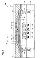
- FIG. 2 is a schematic cross-sectional view showing a schematic configuration of an image sensor for explaining an embodiment of the present invention.
- This imaging device is used by being mounted on an imaging device such as a digital camera or a digital video camera, an imaging module such as an electronic endoscope or a mobile phone, or the like.
- This imaging element has a plurality of photoelectric conversion elements configured as shown in FIG. 1 and a circuit board on which a readout circuit for reading a signal corresponding to the charge generated in the photoelectric conversion layer of each photoelectric conversion element is formed.
- a plurality of photoelectric conversion elements are arranged one-dimensionally or two-dimensionally on the same surface above the circuit board.
- a substrate 101 includes a substrate 101, an insulating layer 102, a connection electrode 103, a pixel electrode 104, a connection portion 105, a connection portion 106, a light receiving layer 107, a counter electrode 108, and a buffer layer. 109, a sealing layer 110, a color filter (CF) 111, a partition 112, a light shielding layer 113, a protective layer 114, a counter electrode voltage supply unit 115, and a readout circuit 116.
- CF color filter
- the pixel electrode 104 has the same function as the electrode 2 of the photoelectric conversion element 10 shown in FIG.
- the counter electrode 108 has the same function as the electrode 5 of the photoelectric conversion element 10 shown in FIG.
- the light receiving layer 107 has the same configuration as the layer provided between the electrode 2 and the electrode 5 of the photoelectric conversion element 10 shown in FIG.
- the sealing layer 110 has the same function as the sealing layer 6 of the photoelectric conversion element 10 illustrated in FIG.
- the pixel electrode 104, a part of the counter electrode 108 facing the pixel electrode 104, a light receiving layer 107 sandwiched between the electrodes, and a part of the buffer layer 109 and the sealing layer 110 facing the pixel electrode 104 are photoelectric conversion elements. Is configured.
- the substrate 101 is a glass substrate or a semiconductor substrate such as Si.
- An insulating layer 102 is formed on the substrate 101.
- a plurality of pixel electrodes 104 and a plurality of connection electrodes 103 are formed on the surface of the insulating layer 102.
- the light receiving layer 107 is a layer common to all the photoelectric conversion elements provided on the plurality of pixel electrodes 104 so as to cover them.
- the counter electrode 108 is one electrode provided on the light receiving layer 107 and common to all the photoelectric conversion elements.
- the counter electrode 108 is formed up to the connection electrode 103 disposed outside the light receiving layer 107 and is electrically connected to the connection electrode 103.
- connection part 106 is embedded in the insulating layer 102 and is a plug or the like for electrically connecting the connection electrode 103 and the counter electrode voltage supply part 115.
- the counter electrode voltage supply unit 115 is formed on the substrate 101 and applies a predetermined voltage to the counter electrode 108 via the connection unit 106 and the connection electrode 103.
- the power supply voltage is boosted by a booster circuit such as a charge pump to supply the predetermined voltage.
- the readout circuit 116 is provided on the substrate 101 corresponding to each of the plurality of pixel electrodes 104, and reads out a signal corresponding to the charge collected by the corresponding pixel electrode 104.
- the reading circuit 116 is configured by, for example, a CCD, a CMOS circuit, a TFT circuit, or the like, and is shielded from light by a light shielding layer (not shown) disposed in the insulating layer 102.
- the readout circuit 116 is electrically connected to the corresponding pixel electrode 104 via the connection unit 105.
- the buffer layer 109 is formed on the counter electrode 108 so as to cover the counter electrode 108.
- the sealing layer 110 is formed on the buffer layer 109 so as to cover the buffer layer 109.
- the color filter 111 is formed at a position facing each pixel electrode 104 on the sealing layer 110.
- the partition wall 112 is provided between the color filters 111 and is for improving the light transmission efficiency of the color filter 111.
- the light shielding layer 113 is formed in a region other than the region where the color filter 111 and the partition 112 are provided on the sealing layer 110, and prevents light from entering the light receiving layer 107 formed outside the effective pixel region.
- the protective layer 114 is formed on the color filter 111, the partition 112, and the light shielding layer 113, and protects the entire image sensor 100.
- the imaging device 100 when light is incident, the light is incident on the light receiving layer 107, and charges are generated here. Holes in the generated charges are collected by the pixel electrode 104, and a voltage signal corresponding to the amount is output to the outside of the image sensor 100 by the readout circuit 116.
- the manufacturing method of the image sensor 100 is as follows.
- connection portions 105 and 106, the plurality of connection electrodes 103, the plurality of pixel electrodes 104, and the insulating layer 102 are formed on the circuit substrate on which the counter electrode voltage supply portion 115 and the readout circuit 116 are formed.
- the plurality of pixel electrodes 104 are arranged on the surface of the insulating layer 102 in a square lattice pattern, for example.
- the light receiving layer 107 is formed on the plurality of pixel electrodes 104 by, for example, a vacuum heating vapor deposition method.
- the counter electrode 108 is formed on the light receiving layer 107 under a vacuum, for example, by sputtering.
- the buffer layer 109 and the sealing layer 110 are sequentially formed on the counter electrode 108 by, for example, a vacuum heating deposition method.
- the protective layer 114 is formed, and the imaging element 100 is completed.
- the photoelectric conversion layer 4 contains a p-type semiconductor compound and two or more different unsubstituted fullerenes.
- the film thickness of the photoelectric conversion layer is not particularly limited, but is preferably 10 nm to 1000 nm, and more preferably 100 nm to 800 nm.
- the photoelectric conversion layer 4 can be formed by a dry film forming method or a wet film forming method.
- the dry film formation method is preferable in that a uniform film formation is easy and impurities are not easily mixed, and that film thickness control and lamination on different materials are easy.
- the dry film forming method include a vacuum vapor deposition method, a sputtering method, an ion plating method, a physical vapor deposition method such as an MBE method, or a CVD method such as plasma polymerization.
- a vacuum deposition method is preferred, and in the case of forming a film by the vacuum deposition method, the production conditions such as the degree of vacuum and the deposition temperature can be set according to conventional methods.
- the decomposition temperature is higher than the vapor deposition possible temperature because thermal decomposition during vapor deposition can be suppressed.
- the degree of vacuum at the time of formation is preferably 1 ⁇ 10 ⁇ 3 Pa or less in consideration of preventing deterioration of element characteristics when the photoelectric conversion layer is formed.
- X10 ⁇ 4 Pa or less is more preferable, and 1 ⁇ 10 ⁇ 4 Pa or less is particularly preferable.
- Examples of the unsubstituted fullerene constituting the photoelectric conversion layer 4 include Cn (n is an integer of 60 or more that geometrically forms a spherical compound), mixed fullerene, fullerene nanotube, and the like. Cn is preferable in terms of absorbance control in the red region. Examples of Cn include fullerene C 60 , fullerene C 70 , fullerene C 76 , fullerene C 78 , fullerene C 80 , fullerene C 82 , fullerene C 84 , fullerene C 90 , fullerene C 96 , fullerene C 240 , fullerene C 540 and the like. It is done. Preferred are fullerene C 60 , fullerene C 70 and fullerene C 76 , and more preferred are fullerene C 60 and fullerene C 70 .
- the photoelectric conversion layer 4 uses two or more kinds of different unsubstituted fullerenes, but at least one of them is Cn (n is an integer of 60 or more that geometrically forms a spherical compound in terms of absorbance control in the red region. ) Is preferable. And it more preferably at least one of a fullerene C 60, more preferably added to the fullerene C 60, is that one at least still another is a fullerene C 70. In addition, in terms of absorbance control in the red region, the number of unsubstituted fullerenes is preferably two, and the two types of unsubstituted fullerenes are preferably fullerene C 60 and fullerene C 70 .
- the content ratio of C 70 in the photoelectric conversion layer 4 is the sum of C 60 and C 70 in order to obtain a preferable photoelectric conversion efficiency by controlling the absorbance in the red region.
- it is preferably 1% by volume to 99% by volume, more preferably 20% by volume to 99% by volume, and still more preferably 40% by volume to 99% by volume.
- the photoelectric conversion layer 4 When the photoelectric conversion layer 4 contains the unsubstituted fullerene, the charges generated by the photoelectric conversion can be quickly transported to the electrode 2 or the electrode 5 via the fullerene molecule. When fullerene molecules are connected and an electron path is formed, the electron transport property is improved and the high-speed response of the photoelectric conversion element can be realized.
- the photoelectric conversion layer 4 preferably contains 50% by volume or more of the fullerene content ratio ⁇ fullerene (a total of two or more types) / p-type semiconductor compound ⁇ 100 (%) ⁇ . Moreover, it is preferable that the content rate of fullerene is contained in the photoelectric converting layer 4 by 85 volume% or less from the viewpoint of maintaining the junction interface and exciton dissociation efficiency of the p-type organic semiconductor.
- the photoelectric conversion layer 4 when a triarylamine compound described in Japanese Patent No. 4213832 is used as a p-type organic semiconductor mixed with an unsubstituted fullerene, a high SN ratio of the photoelectric conversion element can be expressed, preferable. If the ratio of fullerene in the photoelectric conversion layer 4 is too large, the amount of the triarylamine compound decreases and the amount of incident light absorbed decreases. Since this reduces photoelectric conversion efficiency, it is preferable that the said content rate of the fullerene contained in the photoelectric converting layer 4 is a composition of 85 volume% or less.
- the p-type organic semiconductor is a donor-type organic semiconductor (compound), which is mainly represented by a hole-transporting organic compound and refers to an organic compound having a property of easily donating electrons. More specifically, an organic compound having a smaller ionization potential when two organic materials are used in contact with each other. Therefore, any organic compound can be used as the donor organic compound as long as it is an electron-donating organic compound.
- the metal complex etc. which it has as can be used.
- the present invention is not limited thereto, and any organic compound having an ionization potential smaller than that of the organic compound used as the n-type organic semiconductor may be used as the donor organic semiconductor.
- Any organic dye may be used as the p-type organic semiconductor, but preferred are cyanine dye, styryl dye, hemicyanine dye, merocyanine dye (including zero methine merocyanine (simple merocyanine)), trinuclear merocyanine dye, 4 Nuclear merocyanine dye, rhodacyanine dye, complex cyanine dye, complex merocyanine dye, allopolar dye, oxonol dye, hemioxonol dye, squalium dye, croconium dye, azamethine dye, coumarin dye, arylidene dye, anthraquinone dye, triphenylmethane dye, azo Dye, azomethine dye, spiro compound, metallocene dye, fluorenone dye, fulgide dye, perylene dye, perinone dye, phenazine dye, phenothiazine dye, quinone Dye, diphenyl
- the p-type organic semiconductor has a peak wavelength of an absorption spectrum in a chloroform solution (concentration 1 ⁇ 10 ⁇ 5 mol / L) at 600 nm or less, and a maximum molar extinction coefficient of 30000 M ⁇ in the visible region from a wavelength of 400 nm to 700 nm. It is preferably 1 cm ⁇ 1 or more. This is because the higher the molar extinction coefficient, the better from the viewpoint of efficiently using light.
- the peak wavelength is more preferably 450 to 600 nm, still more preferably 480 to 600 nm.
- Maximum molar absorption coefficient is more preferably 35000M -1 cm -1 or more in the visible region, 40000M -1 cm -1 or more is more preferable.
- the p-type organic semiconductor is preferably a compound represented by the following general formula (1).
- L 2 and L 3 each represent a methine group.
- N represents an integer of 0 to 2.
- Ar 1 represents a divalent substituted arylene group or an unsubstituted arylene group.
- Ar 2 , Ar 3 independently represents a substituted aryl group, an unsubstituted aryl group, a substituted alkyl group, an unsubstituted alkyl group, a substituted heteroaryl group, or an unsubstituted heteroaryl group, L 1 is bonded to the following general formula (2) Represents a methine group or a group represented by (3).
- R 1 , R 2 to R 7 each independently represents a hydrogen atom or a substituent, and adjacent ones may be bonded to each other to form a ring.
- M is an integer of 1 to 3
- a plurality of R 1 may be the same or different when m is 2 or more * in General Formula (2) represents a bonding position bonded to L 1, and * in General Formula (3) is This represents the bonding position that binds to L 2 or Ar 1.
- the arylene group represented by Ar 1 is preferably an arylene group having 6 to 30 carbon atoms, and more preferably an arylene group having 6 to 18 carbon atoms.
- the arylene group may have a substituent, and is preferably an arylene group having 6 to 18 carbon atoms which may have an alkyl group having 1 to 4 carbon atoms. Examples include a phenylene group, a naphthylene group, a methylphenylene group, a dimethylphenylene group, and the like, and a phenylene group and a naphthylene group are preferable.
- the aryl groups represented by Ar 2 and Ar 3 are each independently preferably an aryl group having 6 to 30 carbon atoms, and more preferably an aryl group having 6 to 18 carbon atoms.
- the aryl group may have a substituent, preferably an alkyl group having 1 to 4 carbon atoms or an aryl group having 6 to 18 carbon atoms which may have an aryl group having 6 to 18 carbon atoms. is there.
- a phenyl group, a naphthyl group, a tolyl group, an anthryl group, a dimethylphenyl group, a biphenyl group etc. are mentioned, A phenyl group and a naphthyl group are preferable.
- the alkyl group represented by Ar 2 and Ar 3 is preferably an alkyl group having 1 to 6 carbon atoms, and more preferably an alkyl group having 1 to 4 carbon atoms. Examples thereof include a methyl group, an ethyl group, an n-propyl group, an isopropyl group, an n-butyl group, an isobutyl group, and a t-butyl group. A methyl group or an ethyl group is preferable, and a methyl group is more preferable.
- the heteroaryl groups represented by Ar 2 and Ar 3 are each independently preferably a heteroaryl group having 3 to 30 carbon atoms, more preferably a heteroaryl group having 3 to 18 carbon atoms.
- the heteroaryl group may have a substituent, preferably an alkyl group having 1 to 4 carbon atoms or an aryl group having 6 to 18 carbon atoms, and a heteroaryl having 3 to 18 carbon atoms It is a group.
- the heteroaryl group represented by Ar 2 or Ar 3 may have a condensed ring structure, such as a furan ring, a thiophene ring, a selenophene ring, a silole ring, a pyridine ring, a pyrazine ring, a pyrimidine ring, an oxazole ring, a thiazole ring, or a triazole.
- a condensed ring structure selected from a ring, an oxadiazole ring, and a thiadiazole ring (which may be the same) is preferable.
- a bithienothiophene ring is preferred.
- Ar 1 , Ar 2 , Ar 3 , R 1 , R 2 to R 7 may be adjacent to each other to form a ring.
- the ring is preferably a ring formed of a hetero atom, an alkylene group, an aromatic ring or the like.
- an aryl group for example, Ar 1 , Ar 2 , Ar 3 in the general formula (1)
- Ar 1 , Ar 2 , Ar 3 in the general formula (1) is linked via a single bond or a linking group, so that together with a nitrogen atom (N in the general formula (1))
- N nitrogen atom
- linking group examples include a hetero atom (for example, -0-, -S-, etc.), an alkylene group (for example, a methylene group, an ethylene group, etc.), and a group consisting of a combination thereof.
- a methylene group is preferred.
- the ring may further have a substituent, and examples of the substituent include an alkyl group (preferably an alkyl group having 1 to 4 carbon atoms, more preferably a methyl group). They may be connected to each other to further form a ring (for example, a benzene ring).
- R 3 and R 4 are preferably connected to each other to form a ring, and the ring is preferably a benzene ring.
- R 1 is 2 or more
- adjacent ones of the plurality of R 1 can be connected to each other to form a ring, and the ring is preferably a benzene ring.
- R 1 , Ar 2 , Ar 3 has a substituent
- the substituent represented by R 1 , R 2 to R 7 include a halogen atom, an alkyl group (a cycloalkyl group, a bicycloalkyl group, A tricycloalkyl group), a substituted alkyl group, an alkenyl group (including a cycloalkenyl group and a bicycloalkenyl group), an alkynyl group, an aryl group, a substituted aryl group, a heterocyclic group (may be referred to as a heterocyclic group), Cyano group, hydroxy group, nitro group, carboxy group, alkoxy group, aryloxy group, silyloxy group, heterocyclic oxy group, acyloxy group, carbamoyloxy group, alkoxycarbonyl group, aryloxycarbonyl group, amino group (including anilino group) ), Ammonio group, acylamino group
- R 1 , R 2 to R 7 are particularly preferably an alkyl group, a substituted alkyl group, an aryl group, a substituted aryl group, a heteroaryl group, a cyano group, a nitro group, or a halogen atom.
- R 1 is more preferably an alkyl group or an aryl group.
- R 6 and R 7 are more preferably a cyano group. Examples of the substituent of the substituted alkyl group or the substituted aryl group include the substituents listed above.
- An alkyl group preferably an alkyl group having 1 to 4 carbon atoms, more preferably a methyl group
- an aryl group carbon An aryl group of 6 to 18 and more preferably a phenyl group is preferable.
- the alkyl group represented by R 1 and R 2 to R 7 is preferably an alkyl group having 1 to 6 carbon atoms, and more preferably an alkyl group having 1 to 4 carbon atoms. Examples thereof include a methyl group, an ethyl group, an n-propyl group, an isopropyl group, an n-butyl group, an isobutyl group, and a t-butyl group.
- R 2 to R 7 are preferably a methyl group or an ethyl group, and more preferably a methyl group.
- R 1 is preferably a methyl group, an ethyl group or a t-butyl group, more preferably a methyl group or a t-butyl group.
- n is preferably 0 or 1.
- the aryl groups represented by R 1 and R 2 to R 7 are each independently preferably an aryl group having 6 to 30 carbon atoms, and more preferably an aryl group having 6 to 18 carbon atoms.
- the aryl group may have a substituent, preferably an alkyl group having 1 to 4 carbon atoms or an aryl group having 6 to 18 carbon atoms which may have an aryl group having 6 to 18 carbon atoms. is there.
- Examples include a phenyl group, a naphthyl group, an anthracenyl group, a pyrenyl group, a phenanthrenyl group, a methylphenyl group, a dimethylphenyl group, a biphenyl group, and the like, and a phenyl group, a naphthyl group, or an anthracenyl group is preferable.
- the heteroaryl groups represented by R 1 and R 2 to R 7 are each independently preferably a heteroaryl group having 3 to 30 carbon atoms, and more preferably a heteroaryl group having 3 to 18 carbon atoms.
- the heteroaryl group may have a substituent, preferably an alkyl group having 1 to 4 carbon atoms or an aryl group having 6 to 18 carbon atoms, and a heteroaryl having 3 to 18 carbon atoms It is a group.
- the heteroaryl group represented by R 1 , R 2 to R 7 is preferably a heteroaryl group comprising a 5-membered, 6-membered or 7-membered ring or a condensed ring thereof.
- hetero atom contained in the heteroaryl group examples include an oxygen atom, a sulfur atom, and a nitrogen atom.
- ring constituting the heteroaryl group include a furan ring, a thiophene ring, a pyrrole ring, a pyrroline ring, a pyrrolidine ring, an oxazole ring, an isoxazole ring, a thiazole ring, an isothiazole ring, an imidazole ring, an imidazoline ring, and an imidazolidine.
- benzofuran ring isobenzofuran ring, benzothiophene ring, indole ring, indoline ring, isoindole ring, benzoxazole ring, benzothiazole ring, indazole ring, benzimidazole ring, quinoline ring, isoquinoline ring, cinnoline ring, Phthalazine ring, quinazoline ring, quinoxaline ring, dibenzofuran ring, carbazole ring, xanthene ring, acridine ring, phenanthridine ring, phenanthroline ring, phenazine ring, phenoxazine ring, thianthrene ring, thienothiophene ring, indolizine ring, quinolidine ring, A quinuclidine ring, a naphthyridine ring, a pur
- M represents an integer of 1 to 3, preferably 1 or 2, and more preferably 1.
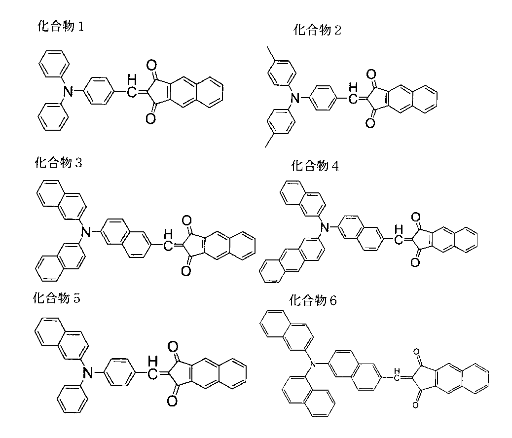
- the following compounds are particularly preferable.
- An electron-donating organic material can be used for the electron blocking layer 3.
- Porphyrin compounds triazole derivatives, oxazizazo Derivatives, imidazole derivatives, polyarylalkane derivatives, pyrazoline derivatives, pyrazolone derivatives, phenylenediamine derivatives, arylamine derivatives, fluorene derivatives, amino-substituted chalcone derivatives, oxazole derivatives, styrylanthracene derivatives, fluorenone derivatives, hydrazone derivatives, silazane derivatives, etc.
- polymers such as phenylene vinylene, fluorene, carbazole, indole, pyrene, pyrrole, picoline, thiophene, acetylene, diacetylene, and derivatives thereof can be used. Even if it is not, it is possible to use a compound having sufficient hole transportability.
- JP-A-2008-72090 the following compounds described in JP-A-2008-72090 are shown, but the present invention is not limited thereto.
- the following Ea represents the electron affinity of the material, and Ip represents the ionization potential of the material. “EB” in EB-1, 2,... Stands for “electronic blocking”.
- An inorganic material can be used as the electron blocking layer 3.
- an inorganic material has a dielectric constant larger than that of an organic material, when it is used for the electron blocking layer 3, a large voltage is applied to the photoelectric conversion layer 4, and the photoelectric conversion efficiency can be increased.
- Materials that can be used as the electron blocking layer 3 include calcium oxide, chromium oxide, chromium copper oxide, manganese oxide, cobalt oxide, nickel oxide, copper oxide, gallium copper oxide, strontium copper oxide, niobium oxide, molybdenum oxide, indium copper oxide, Examples include indium silver oxide and iridium oxide.
- the layer adjacent to the photoelectric conversion layer 4 among the plurality of layers is preferably a layer made of the same material as the p-type organic semiconductor contained in the photoelectric conversion layer 4.
- the same p-type organic semiconductor for the electron blocking layer 3 it is possible to suppress the formation of intermediate levels at the interface between the photoelectric conversion layer 4 and the adjacent layer, and to further suppress the dark current.
- the layer can be a layer made of an inorganic material, or in the case of a plurality of layers, one or more layers can be a layer made of an inorganic material. it can.
- An electron-accepting organic material can be used for the hole blocking layer.
- electron accepting materials include oxadiazole derivatives such as 1,3-bis (4-tert-butylphenyl-1,3,4-oxadiazolyl) phenylene (OXD-7), anthraquinodimethane derivatives, and diphenylquinone derivatives. , Bathocuproine, bathophenanthroline, and derivatives thereof, triazole compounds, tris (8-hydroxyquinolinato) aluminum complexes, bis (4-methyl-8-quinolinato) aluminum complexes, distyrylarylene derivatives, silole compounds, etc. Can do.
- Porphyrin compounds such as DCM (4-dicyanomethylene-2-methyl-6- (4- (dimethylaminostyryl))-4H pyran), and 4H pyran compounds can be used.
- Examples of the material of the electrode 2 include metals, metal oxides, metal nitrides, metal borides, organic conductive compounds, and mixtures thereof. Specific examples include tin oxide, zinc oxide, indium oxide, indium tin oxide (ITO), indium zinc oxide (IZO), indium tungsten oxide (IWO), conductive metal oxides such as titanium oxide, and metal nitrides such as TiN.
- ITO Indium Tin Oxide
- Pt platinum
- silver Ag
- Cr chromium
- Ni nickel
- Al aluminum
- ITO inorganic conductive compounds
- tin oxide antimony-doped tin oxide
- FTO fluorine-doped tin oxide
- ZO gallium-doped zinc oxide
- a step corresponding to the film thickness of the electrode 2 is steep at the end of the electrode 2, there are conspicuous irregularities on the surface of the electrode 2, or minute dust (particles) adhere to the electrode 2 Then, the layer on the electrode 2 becomes thinner than a desired film thickness or cracks are generated.
- the electrode 5 counter electrode 108 is formed on the layer in such a state, a pixel defect such as an increase in dark current or a short circuit occurs due to contact or electric field concentration between the electrode 2 and the electrode 5 in the defective portion. .
- the above-described defects may reduce the adhesion between the electrode 2 and the layer thereon and the heat resistance of the photoelectric conversion element 10.
- the surface roughness Ra of the electrode 2 is preferably 0.6 nm or less.
- Examples of the material of the electrode 5 include metals, metal oxides, metal nitrides, metal borides, organic conductive compounds, and mixtures thereof. Specific examples include tin oxide, zinc oxide, indium oxide, indium tin oxide (ITO), indium zinc oxide (IZO), indium tungsten oxide (IWO), conductive metal oxides such as titanium oxide, and metal nitrides such as TiN.
- ITO Indium Tin Oxide
- Pt platinum
- silver Ag
- Cr chromium
- Ni nickel
- Al aluminum
- ITO inorganic conductive compounds
- tin oxide antimony-doped tin oxide
- FTO fluorine-doped tin oxide
- ZO gallium-doped zinc oxide
- sealing layer 6 The following conditions are required for the sealing layer 6 (sealing layer 110).
- the penetration of factors that degrade the organic photoelectric conversion material, such as water molecules, is prevented, and deterioration of the photoelectric conversion layer 4 is prevented over a long period of storage / use.
- the sealing layer 6 can be composed of a thin film made of a single material. However, by providing a different function for each layer in a multi-layer structure, the stress of the entire sealing layer 6 is reduced, and dust is generated during the manufacturing process. Such effects as the suppression of defects such as cracks and pinholes caused by the above, and the optimization of material development can be expected.
- the sealing layer 6 is formed by laminating a “sealing auxiliary layer” that has a function that is difficult to achieve on the layer that serves the original purpose of preventing the penetration of deterioration factors such as water molecules.
- a two-layer structure can be formed. Although it is possible to have three or more layers, it is preferable that the number of layers is as small as possible in consideration of manufacturing costs.
- sealing layer 6 by atomic layer deposition
- the performance of the photoelectric conversion material is significantly deteriorated due to the presence of deterioration factors such as water molecules. Therefore, it is necessary to cover and seal the entire photoelectric conversion layer with ceramics such as dense metal oxide / metal nitride / metal nitride oxide that does not allow water molecules to permeate, diamond-like carbon (DLC), or the like.
- ceramics such as dense metal oxide / metal nitride / metal nitride oxide that does not allow water molecules to permeate, diamond-like carbon (DLC), or the like.
- DLC diamond-like carbon
- aluminum oxide, silicon oxide, silicon nitride, silicon nitride oxide, a laminated structure thereof, a laminated structure of them and an organic polymer, or the like is used as a sealing layer by various vacuum film forming techniques.
- the imaging element 100 having a pixel size of less than 2 ⁇ m, particularly about 1 ⁇ m if the distance between the color filter 111 and the photoelectric conversion layer, that is, the film thickness of the sealing layer 110 is large, incident light is diffracted / diverged in the sealing layer 110. As a result, color mixing occurs.
- the imaging element 100 having a pixel size of about 1 ⁇ m is preferably a sealing layer material / manufacturing method that does not deteriorate the element performance even when the film thickness of the entire sealing layer 110 is reduced.
- the atomic layer deposition (ALD) method is a kind of CVD method, and adsorption / reaction of organometallic compound molecules, metal halide molecules, and metal hydride molecules, which are thin film materials, onto the substrate surface and unreacted groups contained therein. Is a technique for forming a thin film by alternately repeating decomposition. When the thin film material reaches the substrate surface, it is in the above-mentioned low molecular state, so that the thin film can be grown in a very small space where the low molecule can enter.
- the step portion which was difficult with the conventional thin film forming method, is completely covered (the thickness of the thin film grown on the step portion is the same as the thickness of the thin film grown on the flat portion), that is, the step coverage is very high. Excellent. For this reason, steps due to structures on the substrate surface, minute defects on the substrate surface, particles adhering to the substrate surface, and the like can be completely covered, and such a step portion does not become an intrusion path for a deterioration factor of the photoelectric conversion material.
- the sealing layer 6 is formed by the atomic layer deposition method, the required sealing layer thickness can be effectively reduced as compared with the prior art.
- the sealing layer 6 is formed by the atomic layer deposition method
- a material corresponding to the ceramics preferable for the sealing layer 6 described above can be selected as appropriate.
- the photoelectric conversion layer of the present invention uses a photoelectric conversion material, it is limited to a material capable of growing a thin film at a relatively low temperature so that the photoelectric conversion material does not deteriorate.
- a dense aluminum oxide thin film can be formed at less than 200 ° C. at which the photoelectric conversion material does not deteriorate.
- an aluminum oxide thin film can be formed even at about 100 ° C.
- Silicon oxide and titanium oxide are also preferable because a dense thin film can be formed at less than 200 ° C., similarly to aluminum oxide, by appropriately selecting materials.
- the thin film formed by the atomic layer deposition method can achieve a high-quality thin film formation at a low temperature that is unmatched from the viewpoint of step coverage and denseness.
- the physical properties of the thin film material may be deteriorated by chemicals used in the photolithography process.
- an aluminum oxide thin film formed by atomic layer deposition is amorphous, the surface is eroded by an alkaline solution such as a developer or a stripping solution.
- a thin film having excellent chemical resistance must be formed on the aluminum oxide thin film formed by the atomic layer deposition method, that is, a sealing auxiliary layer serving as a functional layer for protecting the sealing layer 6 is provided. I need it.
- a thin film formed by a CVD method such as an atomic layer deposition method has many examples in which internal stress has a very large tensile stress, and a process in which intermittent heating and cooling are repeated like a semiconductor manufacturing process,
- the storage / use in a high-temperature / high-humidity atmosphere for a long time may cause deterioration of the thin film itself with cracks.
- a metal having excellent chemical resistance formed by a physical vapor deposition (PVD) method such as a sputtering method.
- PVD physical vapor deposition
- a configuration in which a sealing auxiliary layer including any one of ceramics such as oxide, metal nitride, and metal nitride oxide is provided is preferable.
- the first sealing layer is formed by the atomic layer deposition method, and is formed on the first sealing layer by the PVD method and is any one of metal oxide, metal nitride, and metal nitride oxide.
- One containing one is defined as a second sealing layer. If it carries out like this, it will become easy to improve the chemical resistance of the sealing layer 6 whole.
- ceramics formed by PVD methods such as sputtering often have a large compressive stress, and can cancel the tensile stress of the first sealing layer formed by atomic layer deposition. Therefore, not only the stress of the sealing layer 6 is alleviated and the reliability of the sealing layer 6 itself is increased, but the stress of the sealing layer 6 deteriorates or destroys the performance of the photoelectric conversion layer or the like. Occurrence can be remarkably suppressed.
- the first sealing layer preferably includes a second sealing layer formed by sputtering and containing any one of aluminum oxide, silicon oxide, silicon nitride, and silicon nitride oxide. .
- the first sealing layer preferably has a thickness of 0.05 ⁇ m or more and 0.5 ⁇ m or less.
- the first sealing layer preferably contains any of aluminum oxide, silicon oxide, and titanium oxide.
- Example 1 A solid-state imaging device including a photoelectric conversion device having a photoelectric conversion layer and an electron blocking layer between a pair of electrodes was produced as follows. That is, an amorphous ITO film is formed by sputtering on a silicon substrate on which a CMOS circuit is formed as a readout circuit, and one pixel is present on each CMOS photodiode (PD) by photolithography. Patterning was performed to form a pixel electrode (lower electrode). On top of this, the EB-3 was deposited by vacuum heating vapor deposition to form an electron blocking layer having a thickness of 100 nm.
- the compound 6 p-type semiconductor compound
- fullerene C 60 and fullerene C 70 were each formed by vacuum heating vapor deposition by three-source vapor deposition to form a 400 nm thick photoelectric conversion layer.
- the volume ratio of fullerene C 60 and fullerene C 70 in the photoelectric conversion layer was set to 3: 1.
- the volume ratio of the compound 6-fullerene of the photoelectric conversion layer (the sum of the fullerene C 60 and fullerene C 70) was 1: 2.
- amorphous ITO was formed into a film having a thickness of 10 nm by sputtering as an upper electrode to form a transparent electrode (upper electrode), thereby producing a solid-state imaging device.
- a silicon oxide film formed by heat evaporation was formed as a sealing layer, and an aluminum oxide film was further formed thereon by the ALD method.
- the absorption spectrum of Compound 6 in a chloroform solution was measured by UV-2550 manufactured by Shimadzu Corporation, and the peak wavelength was 539 nm. Further, the maximum molar extinction coefficient in the visible region from a wavelength of 400 nm to 700 nm was 50000 M ⁇ 1 cm ⁇ 1 .
- Example 2 In Example 1, a solid-state imaging device was produced in the same manner as in Example 1 except that the volume ratio of fullerene C 60 and fullerene C 70 in the photoelectric conversion layer was 1: 1.
- Example 3 In Example 1, the volume ratio of the fullerene C 60 and fullerene C 70 in the photoelectric conversion layer is 1: Other than changing as a 3, to prepare a solid-state imaging device in the same manner as in Example 1.
- Example 4 In Example 1, a solid-state imaging device was fabricated in the same manner as in Example 1 except that the volume ratio of fullerene C 60 and fullerene C 70 in the photoelectric conversion layer was 49: 2.
- Example 5 a solid-state imaging device was produced in the same manner as in Example 1 except that the volume ratio of fullerene C 60 and fullerene C 70 in the photoelectric conversion layer was 1:99.
- Example 6 In Example 1, a solid-state imaging device was produced in the same manner as in Example 1 except that the compound 6 in the photoelectric conversion layer was changed to the compound 7.
- Example 7 a solid-state imaging device was produced in the same manner as in Example 3 except that the compound 6 in the photoelectric conversion layer was changed to the compound 7.
- Example 8 In Example 1, fullerenes in the photoelectric conversion layer were formed in the same manner as in Example 1 except that the four-source deposition was performed so that the volume ratio of fullerene C 60 , fullerene C 70, and fullerene C 76 was 98: 4: 1. A solid-state image sensor was produced.
- Example 1 In Example 1, except that the volume ratio of fullerene C 60 and fullerene C 70 was 1: 0 in the photoelectric conversion layer (that is, only compound 6 and fullerene C 60 were co-deposited). In the same manner as in Example 1, a solid-state imaging device was produced.
- Example 2 In Example 1, except that the volume ratio of fullerene C 60 and fullerene C 70 was 0: 1 in the photoelectric conversion layer (that is, only compound 6 and fullerene C 70 were co-deposited). In the same manner as in Example 1, a solid-state imaging device was produced.
- the absorbance of each photoelectric conversion layer in each Example and Comparative Example was measured with U-3310 manufactured by Hitachi High-Technologies Corporation.
- the ratio of absorbance A ( ⁇ nm) in the red region (absorption long wavelength end region) is shown in Table 1 below.
- Table 1 below shows the external quantum efficiency (relative value when the comparative example 1 is set to 100) at a wavelength of 630 nm of each element. Note that an electric field of 2 ⁇ 10 5 V / cm was applied to each element during the external quantum efficiency measurement.
- Table 1 below shows the absorbance of each element at a wavelength of 680 nm (relative value when Comparative Example 1 is 100).
- Example 3 Moreover, in Example 1, production of fullerene C 60 in the photoelectric conversion layer and PCBM, which is a substituted fullerene, was attempted so that the volume ratio was 1: 1. However, the deposition rate of PCBM decreased during the deposition, and the target The film thickness could not be reached and the device could not be fabricated. As described above, when a substituted fullerene film is formed, it is difficult to keep the film formation rate constant due to the influence of decomposition or the like, and in the production of a photoelectric conversion film containing an unsubstituted fullerene and a substituted fullerene, the fullerene content ratio must be finely controlled. Is difficult and the absorbance in the red region cannot be controlled.
- PCBM (compound below)
- a photoelectric conversion element in which the absorbance in the red region is changed and the long wavelength end of absorption is controlled can be obtained.
- an imaging element with improved color reproducibility can be obtained.
Landscapes
- Engineering & Computer Science (AREA)
- Chemical & Material Sciences (AREA)
- Physics & Mathematics (AREA)
- Nanotechnology (AREA)
- Spectroscopy & Molecular Physics (AREA)
- Materials Engineering (AREA)
- Mathematical Physics (AREA)
- Theoretical Computer Science (AREA)
- Crystallography & Structural Chemistry (AREA)
- Light Receiving Elements (AREA)
- Solid State Image Pick-Up Elements (AREA)
- Electroluminescent Light Sources (AREA)
Abstract
Description
特許文献1には、光電変換効率の向上を目的に、p型半導体とn型半導体からなる光電変換層を一対の電極で挟んだ光電変換素子を含有し、該光電変換層にフラーレン又はフラーレン誘導体を含有する撮像素子を開示している。しかしながら、撮像素子の色再現性を向上させる上で、赤色領域(波長600nm以上)の吸光度を制御して吸収の長波長端を制御することが求められるが、特許文献1に記載の方法では長波長端を制御する光電変換素子を作製することは困難であった。
また、特許文献2及び3には、光電変換層に2種類のフラーレンを混合する光電池を開示されており、更に、熱安定性を向上させるために、光電変換層を置換フラーレンと非置換フラーレンを混合する構成とすることも記載されている。しかしながら、特許文献2及び3では、2種のフラーレンのうち一方は置換基を有するフラーレンであり、無置換のフラーレンを2種以上用いることは記載されていない。また、光電池では、撮像素子と異なり、色再現性の向上の必要性はない。実際に、特許文献2及び3には、赤外領域の吸収の長波長端制御に関する記載はなく、また、撮像素子用の光電変換層への適用可能性について具体的な記載も示唆もない。
[1]
一対の電極と、前記一対の電極間に配置された光電変換層とを含む光電変換素子であって、前記光電変換層がp型半導体化合物と二種類以上の異なる無置換フラーレンを含む光電変換素子。
[2]
前記二種類以上の無置換フラーレンの少なくとも一つがCn(nは幾何学的に球状化合物を形成する60以上の整数)である[1]に記載の光電変換素子。
[3]
前記二種類以上の無置換フラーレンの一つがC60である[2]に記載の光電変換素子。
[4]
前記二種類以上の無置換フラーレンの更にもう一つがC70である[3]に記載の光電変換素子。
[5]
前記無置換フラーレンが二種類である[1]~[4]のいずれか一項に記載の光電変換素子。
[6]
前記二種類の無置換フラーレンがC60とC70である[5]に記載の光電変換素子。
[7]
前記光電変換層におけるC70の含有比率が、前記C60とC70の合計に対して20体積%以上99体積%以下である[4]又は[6]に記載の光電変換素子。
[8]
前記p型半導体化合物が、クロロホルム溶液中での吸収スペクトルのピーク波長を600nm以下に有し、波長400nmから700nmまでの可視領域において最大モル吸光係数が30000M-1cm-1以上である[1]~[7]のいずれか一項に記載の光電変換素子。
[9]
波長λnmの吸光度をA(λ)としたときに、A(650)/A(680)>1.62である[1]~[8]のいずれか一項に記載の光電変換素子。
[10]
波長λnmの吸光度をA(λ)としたときに、A(630)/A(680)>2.58である[1]~[9]のいずれか一項に記載の光電変換素子。
[11]
前記光電変換層における前記p型半導体化合物と前記無置換フラーレンとの含有比率((前記二種類以上の無置換フラーレンの合計の含有量)/(前記p型半導体化合物の含有量)×100(%))が、50%(体積比率)以上である[1]~[10]のいずれか一項に記載の光電変換素子。
[12]
前記光電変換層が乾式成膜法により成膜されたものである[1]~[11]のいずれか一項に記載の光電変換素子。
[13]
前記乾式成膜法が真空蒸着法である[12]に記載の光電変換素子。
[14]
[1]~[13]のいずれか一項に記載の光電変換素子の製造方法であって、前記p型半導体化合物と前記二種類以上の異なる無置換フラーレンを真空加熱蒸着により共蒸着して前記光電変換層を形成する工程を含む、光電変換素子の製造方法。
[15]
[1]~[13]のいずれか一項に記載の光電変換素子を含む光センサ。
[16]
[1]~[13]のいずれか一項に記載の光電変換素子を含む撮像素子。
<光電変換素子>
本発明の光電変換素子は、一対の電極と、前記一対の電極間に配置された光電変換層とを含む光電変換素子であって、前記光電変換層がp型半導体化合物と二種類以上の異なる無置換フラーレンを含む。
光電変換層に二種類以上の無置換フラーレンを含有させることにより、波長600nm以上の赤色領域(好ましくは600nm以上750nm以下)の吸光度を変化させ、吸収の長波長端を制御することができる。このため、撮像素子に最適な赤色領域の分光特性を得ることができ、本発明の光電変換素子を用いることで撮像素子の色再現性を向上させることができる。
赤色領域の吸光度としては、波長600nm以上650nm以下の吸光度をできるだけ向上させ、波長680nm以上の吸光度をできるだけ小さいまま維持することが好ましい。これにより、赤外光カットフィルターや信号処理による赤色領域の補正を必要とせず、二種類以上の異なる無置換フラーレンの混合比を変えることで赤色領域の吸光度を微調整し、吸収の長波長端を自由に変化させることができる。
赤色領域の吸光度としては、波長λnmの吸光度をA(λ)としたときに、A(650)/A(680)>1.62であることが好ましく、A(650)/A(680)>1.70であることがより好ましい。また、A(630)/A(680)>2.58であることが好ましく、A(630)/A(680)>2.71であることがより好ましい。赤色領域の吸光度が上記関係を満足する場合、吸収の長波長端が好ましく制御されて撮像素子に適用するのに適した分光特性を得ることができる。そのため、撮像素子の色再現性の向上にとって好ましい。
赤色領域の吸光度を制御した本発明の光電変換素子を用いることで、色再現性に優れた撮像素子を得ることができる。
図2は、本発明の一実施形態を説明するための撮像素子の概略構成を示す断面模式図である。この撮像素子は、デジタルカメラ、デジタルビデオカメラ等の撮像装置、電子内視鏡、携帯電話機等の撮像モジュール等に搭載して用いられる。
光電変換層4はp型半導体化合物と二種類以上の異なる無置換フラーレンを含む。
光電変換層の膜厚は特に制限されないが、10nm~1000nmが好ましく、100nm~800nmがより好ましい。
Cnとしては、フラーレンC60、フラーレンC70、フラーレンC76、フラーレンC78、フラーレンC80、フラーレンC82、フラーレンC84、フラーレンC90、フラーレンC96、フラーレンC240、フラーレンC540などが挙げられる。好ましくは、フラーレンC60、フラーレンC70、フラーレンC76であり、より好ましくはフラーレンC60、フラーレンC70である。
ピーク波長は、450~600nmがより好ましく、480~600nmが更に好ましい。可視領域における最大モル吸光係数は35000M-1cm-1以上がより好ましく、40000M-1cm-1以上が更に好ましい。


該環は更に置換基を有していてもよく、該置換基としては、アルキル基(好ましくは炭素数1~4のアルキル基、より好ましくはメチル基)が挙げられ、複数の該置換基が互いに連結して更に環(例えば、ベンゼン環など)を形成してもよい。
また、R3及びR4が互いに連結して環を形成していることも好ましく、該環としてはベンゼン環が好ましい。
更にまた、R1については、複数ある場合(mが2以上)に該複数のR1のうち隣接するものは互いに連結して環を形成することができ、該環としてはベンゼン環が好ましい。
上記置換アルキル基や置換アリール基が有する置換基としては、上記で列挙した置換基が挙げられ、アルキル基(好ましくは炭素数1~4のアルキル基、より好ましくはメチル基)やアリール基(炭素数6~18のアリール基、より好ましくはフェニル基)が好ましい。
nは0又は1が好ましい。
縮合環としては、ベンゾフラン環、イソベンゾフラン環、ベンゾチオフェン環、インドール環、インドリン環、イソインドール環、ベンゾオキサゾール環、ベンゾチアゾール環、インダゾール環、ベンゾイミダゾール環、キノリン環、イソキノリン環、シンノリン環、フタラジン環、キナゾリン環、キノキサリン環、ジベンゾフラン環、カルバゾール環、キサンテン環、アクリジン環、フェナントリジン環、フェナントロリン環、フェナジン環、フェノキサジン環、チアントレン環、チエノチオフェン環、インドリジン環、キノリジン環、キヌクリジン環、ナフチリジン環、プリン環、プテリジン環等が挙げられる。


電子ブロッキング層3には、電子供与性有機材料を用いることができる。具体的には、低分子材料では、N,N’-ビス(3-メチルフェニル)-(1,1’-ビフェニル)-4,4’-ジアミン(TPD)や4,4’-ビス[N-(ナフチル)-N-フェニル-アミノ]ビフェニル(α-NPD)等の芳香族ジアミン化合物、オキサゾール、オキサジアゾール、トリアゾール、イミダゾール、イミダゾロン、スチルベン誘導体、ピラゾリン誘導体、テトラヒドロイミダゾール、ポリアリールアルカン、ブタジエン、4,4’,4”-トリス(N-(3-メチルフェニル)N-フェニルアミノ)トリフェニルアミン(m-MTDATA)、ポルフィン、テトラフェニルポルフィン銅、フタロシアニン、銅フタロシアニン、チタニウムフタロシアニンオキサイド等のポリフィリン化合物、トリアゾール誘導体、オキサジザゾール誘導体、イミダゾール誘導体、ポリアリールアルカン誘導体、ピラゾリン誘導体、ピラゾロン誘導体、フェニレンジアミン誘導体、アリールアミン誘導体、フルオレン誘導体、アミノ置換カルコン誘導体、オキサゾール誘導体、スチリルアントラセン誘導体、フルオレノン誘導体、ヒドラゾン誘導体、シラザン誘導体などを用いることができ、高分子材料では、フェニレンビニレン、フルオレン、カルバゾール、インドール、ピレン、ピロール、ピコリン、チオフェン、アセチレン、ジアセチレン等の重合体や、その誘導体を用いることができる。電子供与性化合物でなくとも、充分な正孔輸送性を有する化合物であれば用いることは可能である。

正孔ブロッキング層には、電子受容性有機材料を用いることができる。電子受容性材料としては、1,3-ビス(4-tert-ブチルフェニル-1,3,4-オキサジアゾリル)フェニレン(OXD-7)等のオキサジアゾール誘導体、アントラキノジメタン誘導体、ジフェニルキノン誘導体、バソクプロイン、バソフェナントロリン、及びこれらの誘導体、トリアゾール化合物、トリス(8-ヒドロキシキノリナート)アルミニウム錯体、ビス(4-メチル-8-キノリナート)アルミニウム錯体、ジスチリルアリーレン誘導体、シロール化合物などを用いることができる。また、電子受容性有機材料でなくとも、十分な電子輸送性を有する材料ならば使用することは可能である。ポルフィリン系化合物や、DCM(4-ジシアノメチレン-2-メチル-6-(4-(ジメチルアミノスチリル))-4Hピラン)等のスチリル系化合物、4Hピラン系化合物を用いることができる。
電極2(画素電極104)の材料としては、例えば、金属、金属酸化物、金属窒化物、金属硼化物、有機導電性化合物、これらの混合物等が挙げられる。具体例としては、酸化錫、酸化亜鉛、酸化インジウム、酸化インジウム錫(ITO)、酸化インジウム亜鉛(IZO)、酸化インジウムタングステン(IWO)、酸化チタン等の導電性金属酸化物、TiN等の金属窒化物、金(Au)、白金(Pt)、銀(Ag)、クロム(Cr)、ニッケル(Ni)、アルミニウム(Al)等の金属、更にこれらの金属と導電性金属酸化物との混合物又は積層物、ポリアニリン、ポリチオフェン、ポリピロール等の有機導電性化合物、これらとITOとの積層物、などが挙げられる。透明導電膜の材料として特に好ましいのは、ITO、IZO、酸化錫、アンチモンドープ酸化錫(ATO)、弗素ドープ酸化錫(FTO)、酸化亜鉛、アンチモンドープ酸化亜鉛(AZO)、ガリウムドープ酸化亜鉛(GZO)のいずれかの材料である。
電極5(対向電極108)の材料としては、例えば、金属、金属酸化物、金属窒化物、金属硼化物、有機導電性化合物、これらの混合物等が挙げられる。具体例としては、酸化錫、酸化亜鉛、酸化インジウム、酸化インジウム錫(ITO)、酸化インジウム亜鉛(IZO)、酸化インジウムタングステン(IWO)、酸化チタン等の導電性金属酸化物、TiN等の金属窒化物、金(Au)、白金(Pt)、銀(Ag)、クロム(Cr)、ニッケル(Ni)、アルミニウム(Al)等の金属、更にこれらの金属と導電性金属酸化物との混合物又は積層物、ポリアニリン、ポリチオフェン、ポリピロール等の有機導電性化合物、これらとITOとの積層物、などが挙げられる。透明導電膜の材料として特に好ましいのは、ITO、IZO、酸化錫、アンチモンドープ酸化錫(ATO)、弗素ドープ酸化錫(FTO)、酸化亜鉛、アンチモンドープ酸化亜鉛(AZO)、ガリウムドープ酸化亜鉛(GZO)のいずれかの材料である。
封止層6(封止層110)としては次の条件が求められる。
第一に、素子の各製造工程において溶液、プラズマなどに含まれる有機の光電変換材料を劣化させる因子の浸入を阻止して光電変換層を保護することが挙げられる。
第二に、素子の製造後に、水分子などの有機の光電変換材料を劣化させる因子の浸入を阻止して、長期間の保存/使用にわたって、光電変換層4の劣化を防止する。
第三に、封止層6を形成する際は既に形成された光電変換層を劣化させない。
第四に、入射光は封止層6を通じて光電変換層4に到達するので、光電変換層4で検知する波長の光に対して封止層6は透明でなくてはならない。
光電変換材料は水分子などの劣化因子の存在で顕著にその性能が劣化してしまう。そのために、水分子を浸透させない緻密な金属酸化物・金属窒化物・金属窒化酸化物などセラミクスやダイヤモンド状炭素(DLC)などで光電変換層全体を被覆して封止することが必要である。従来から、酸化アルミニウム、酸化珪素、窒化珪素、窒化酸化珪素やそれらの積層構成、それらと有機高分子の積層構成などを封止層として、各種真空成膜技術で形成されている。もっとも、これら従来の封止層は、基板表面の構造物、基板表面の微小欠陥、基板表面に付着したパーティクルなどによる段差において、薄膜の成長が困難なので(段差が影になるので)平坦部と比べて膜厚が顕著に薄くなる。このために段差部分が劣化因子の浸透する経路になってしまう。この段差を封止層で完全に被覆するには、平坦部において1μm以上の膜厚になるように成膜して、封止層全体を厚くすることが好ましい。
原子層堆積法により形成した薄膜は、段差被覆性、緻密性という観点からは比類なく良質な薄膜形成を低温で達成できる。もっとも、薄膜材料の物性が、フォトリソグラフィ工程で使用する薬品で劣化してしまうことがある。例えば、原子層堆積法で成膜した酸化アルミニウム薄膜は非晶質なので、現像液や剥離液のようなアルカリ溶液で表面が侵食されてしまう。この場合は、原子層堆積法で形成した酸化アルミニウム薄膜上に、耐薬品性に優れる薄膜を形成しなくてはならず、すなわち、封止層6を保護する機能層となる封止補助層が必要になる。
以下のとおり、一対の電極間に、光電変換層と電子ブロッキング層とを有する光電変換素子を含む固体撮像素子を作製した。
即ち、読み出し回路としてCMOS回路が形成されたシリコン基板上に、アモルファス性ITOをスパッタ法により成膜後、フォトリソグラフィーによりCMOSのフォトダイオード(PD)の上にそれぞれ1つずつ画素が存在するようにパターニングして画素電極(下部電極)とした。その上に、前記EB-3を真空加熱蒸着により成膜して厚み100nmの電子ブロッキング層を形成した。その上に、前記化合物6(p型半導体化合物)とフラーレンC60とフラーレンC70を三源蒸着にてそれぞれ真空加熱蒸着により成膜して、厚み400nmの光電変換層を形成した。光電変換層中のフラーレンC60とフラーレンC70との体積比率は3:1となるようにした。光電変換層中の化合物6とフラーレン(フラーレンC60及びフラーレンC70の合計)との体積比率は1:2であった。光電変換層上に、上部電極としてスパッタ法によりアモルファス性ITOを厚み10nmで成膜して透明電極(上部電極)とすることにより、固体撮像素子を作製した。上部電極上には、封止層として加熱蒸着による酸化シリコン膜を形成し、更にその上にALD法により酸化アルミニウム膜を形成した。
実施例1において、光電変換層中のフラーレンC60とフラーレンC70との体積比率が1:1となるようにした以外は、実施例1と同様にして固体撮像素子を作製した。
実施例1において、光電変換層中のフラーレンC60とフラーレンC70との体積比率が1:3となるようにした以外は、実施例1と同様にして固体撮像素子を作製した。
実施例1において、光電変換層中のフラーレンC60とフラーレンC70との体積比率が49:2となるようにした以外は、実施例1と同様にして固体撮像素子を作製した。
実施例1において、光電変換層中のフラーレンC60とフラーレンC70との体積比率が1:99となるようにした以外は、実施例1と同様にして固体撮像素子を作製した。
実施例1において、光電変換層中の化合物6が前記化合物7となるようにした以外は、実施例1と同様にして固体撮像素子を作製した。
実施例3において、光電変換層中の化合物6が前記化合物7となるようにした以外は、実施例3と同様にして固体撮像素子を作製した。
実施例1において、光電変換層中のフラーレンをフラーレンC60とフラーレンC70とフラーレンC76の体積比率が98:4:1となるように四源蒸着した以外は、実施例1と同様にして固体撮像素子を作製した。
実施例1において、光電変換層中をフラーレンC60とフラーレンC70との体積比率が1:0となるようにした(即ち、化合物6とフラーレンC60のみを共蒸着した)以外は、実施例1と同様にして固体撮像素子を作製した。
実施例1において、光電変換層中をフラーレンC60とフラーレンC70との体積比率が0:1となるようにした(即ち、化合物6とフラーレンC70のみを共蒸着した)以外は、実施例1と同様にして固体撮像素子を作製した。
また、各素子の波長630nmにおける外部量子効率(比較例1を100としたときの相対値)を下記表1に示す。なお、外部量子効率測定の際に各素子には2×10⁵V/cmの電場を印加した。また、各素子の波長680nmの吸光度(比較例1を100としたときの相対値)を下記表1に示す。

また、実施例1において、光電変換層中のフラーレンC60と置換フラーレンであるPCBMを体積比率が1:1となるように作製を試みたが、蒸着途中でPCBMの蒸着レートが低下し、目標膜厚に到達できず素子を作製できなかった。このように、置換フラーレンを成膜する場合、分解などの影響で成膜レートを一定にすることが難しく、無置換フラーレンと置換フラーレンを含む光電変換膜作成において、フラーレン含有比率を細かく制御することは困難であり、赤色領域の吸光度を制御することができない。
PCBM:(下記に化合物)

本出願は、2010年3月31日出願の日本特許出願(特願2010-084406)及び、2010年12月27日出願の日本特許出願(特願2010-291376)に基づくものであり、その内容はここに参照として取り込まれる。
2、5 電極
3 電子ブロッキング層
4 光電変換層
6 封止層
10 光電変換素子
Claims (16)
- 一対の電極と、前記一対の電極間に配置された光電変換層とを含む光電変換素子であって、前記光電変換層がp型半導体化合物と二種類以上の異なる無置換フラーレンを含む光電変換素子。
- 前記二種類以上の無置換フラーレンの少なくとも一つがCn(nは幾何学的に球状化合物を形成する60以上の整数)である請求項1に記載の光電変換素子。
- 前記二種類以上の無置換フラーレンの一つがC60である請求項2に記載に記載の光電変換素子。
- 前記二種類以上の無置換フラーレンの更にもう一つがC70である請求項3に記載の光電変換素子。
- 前記無置換フラーレンが二種類である請求項1~4のいずれか一項に記載に記載の光電変換素子。
- 前記二種類の無置換フラーレンがC60とC70である請求項5に記載の光電変換素子。
- 前記光電変換層におけるC70の含有比率が、前記C60とC70の合計に対して20体積%以上99体積%以下である請求項4又は6に記載の光電変換素子。
- 前記p型半導体化合物が、クロロホルム溶液中での吸収スペクトルのピーク波長を600nm以下に有し、波長400nmから700nmまでの可視領域において最大モル吸光係数が30000M-1cm-1以上である請求項1~7のいずれか一項に記載に記載の光電変換素子。
- 波長λnmの吸光度をA(λ)としたときに、A(650)/A(680)>1.62である請求項1~8のいずれか一項に記載に記載の光電変換素子。
- 波長λnmの吸光度をA(λ)としたときに、A(630)/A(680)>2.58である請求項1~9のいずれか一項に記載に記載の光電変換素子。
- 前記光電変換層における前記p型半導体化合物と前記無置換フラーレンとの含有比率((前記二種類以上の無置換フラーレンの合計の含有量)/(前記p型半導体化合物の含有量)×100(%))が、50%(体積比率)以上である請求項1~10のいずれか一項に記載に記載の光電変換素子。
- 前記光電変換層が乾式成膜法により成膜されたものである請求項1~11のいずれか一項に記載に記載の光電変換素子。
- 前記乾式成膜法が真空蒸着法である請求項12に記載に記載の光電変換素子。
- 請求項1~13のいずれか一項に記載の光電変換素子の製造方法であって、前記p型半導体化合物と前記二種類以上の異なる無置換フラーレンを真空加熱蒸着により共蒸着して前記光電変換層を形成する工程を含む、光電変換素子の製造方法。
- 請求項1~13のいずれか一項に記載の光電変換素子を含む光センサ。
- 請求項1~13のいずれか一項に記載の光電変換素子を含む撮像素子。
Priority Applications (2)
| Application Number | Priority Date | Filing Date | Title |
|---|---|---|---|
| US13/638,000 US8822808B2 (en) | 2010-03-31 | 2011-03-24 | Photoelectric conversion device, method for manufacturing the same, photo sensor and imaging device |
| KR1020127025587A KR20130038208A (ko) | 2010-03-31 | 2011-03-24 | 광전 변환 소자, 그 제조 방법, 광센서, 및 촬상 소자 |
Applications Claiming Priority (4)
| Application Number | Priority Date | Filing Date | Title |
|---|---|---|---|
| JP2010084406 | 2010-03-31 | ||
| JP2010-084406 | 2010-03-31 | ||
| JP2010291376A JP5288640B2 (ja) | 2010-03-31 | 2010-12-27 | 撮像素子及びその製造方法 |
| JP2010-291376 | 2010-12-27 |
Publications (1)
| Publication Number | Publication Date |
|---|---|
| WO2011125527A1 true WO2011125527A1 (ja) | 2011-10-13 |
Family
ID=44762481
Family Applications (1)
| Application Number | Title | Priority Date | Filing Date |
|---|---|---|---|
| PCT/JP2011/057251 Ceased WO2011125527A1 (ja) | 2010-03-31 | 2011-03-24 | 光電変換素子、その製造方法、光センサ、及び撮像素子 |
Country Status (4)
| Country | Link |
|---|---|
| US (1) | US8822808B2 (ja) |
| JP (1) | JP5288640B2 (ja) |
| KR (1) | KR20130038208A (ja) |
| WO (1) | WO2011125527A1 (ja) |
Cited By (3)
| Publication number | Priority date | Publication date | Assignee | Title |
|---|---|---|---|---|
| WO2013065665A1 (ja) * | 2011-10-31 | 2013-05-10 | 富士フイルム株式会社 | 撮像素子 |
| US10692913B2 (en) | 2015-06-25 | 2020-06-23 | Sony Corporation | Photoelectric conversion element, image pickup element, laminated image pickup element, and image pickup device |
| US12074178B2 (en) | 2018-12-28 | 2024-08-27 | Sony Semiconductor Solutions Corporation | Imaging device and electronic apparatus |
Families Citing this family (12)
| Publication number | Priority date | Publication date | Assignee | Title |
|---|---|---|---|---|
| JP5516153B2 (ja) * | 2010-07-05 | 2014-06-11 | コニカミノルタ株式会社 | 有機光電変換素子、それを用いた太陽電池及び光センサアレイ |
| TW201600574A (zh) * | 2014-06-30 | 2016-01-01 | Fujifilm Corp | 近紅外線吸收性組成物、近紅外線截止濾波器、近紅外線截止濾波器的製造方法、固體攝像元件、照相機模組 |
| US10978514B2 (en) * | 2015-10-06 | 2021-04-13 | Sony Semiconductor Solutions Corporation | Solid-state imaging device, and method of manufacturing solid-state imaging device |
| JP6750635B2 (ja) | 2016-01-08 | 2020-09-02 | 株式会社ニコン | 撮像素子および撮像装置 |
| WO2018147202A1 (ja) * | 2017-02-07 | 2018-08-16 | キヤノン株式会社 | 光電変換素子、及びこれを用いた光エリアセンサ、撮像素子、撮像装置 |
| JP7086573B2 (ja) * | 2017-11-17 | 2022-06-20 | キヤノン株式会社 | 光電変換素子、及びこれを用いた光エリアセンサ、撮像素子、撮像装置 |
| CN110301052B (zh) * | 2017-02-07 | 2023-12-12 | 佳能株式会社 | 光电转换元件、和使用其的光学区域传感器、图像拾取元件和图像拾取设备 |
| JP7039285B2 (ja) * | 2017-02-07 | 2022-03-22 | キヤノン株式会社 | 光電変換素子、及びこれを用いた光エリアセンサ、撮像素子、撮像装置 |
| WO2018207420A1 (ja) * | 2017-05-08 | 2018-11-15 | ソニー株式会社 | 有機光電変換素子 |
| CN108933182B (zh) * | 2017-05-24 | 2020-05-15 | 清华大学 | 光探测器 |
| JP7283148B2 (ja) * | 2019-03-14 | 2023-05-30 | 富士通株式会社 | 赤外線検出器、これを用いた撮像装置、及び赤外線検出器の製造方法 |
| KR102819931B1 (ko) | 2019-08-01 | 2025-06-11 | 삼성전자주식회사 | 센서 및 전자 장치 |
Citations (3)
| Publication number | Priority date | Publication date | Assignee | Title |
|---|---|---|---|---|
| WO2008081845A1 (ja) * | 2006-12-27 | 2008-07-10 | Frontier Carbon Corporation | フラーレン誘導体を原料とするフラーレン膜およびフラーレン重合体ならびにそれらの製造方法 |
| JP2008537846A (ja) * | 2005-03-21 | 2008-09-25 | コナルカ テクノロジーズ インコーポレイテッド | ポリマー光電池 |
| JP2009105336A (ja) * | 2007-10-25 | 2009-05-14 | Mitsubishi Chemicals Corp | 膜の製造方法、有機電子素子の製造方法及びナフタロシアニン膜 |
Family Cites Families (14)
| Publication number | Priority date | Publication date | Assignee | Title |
|---|---|---|---|---|
| JPH05335614A (ja) | 1992-06-03 | 1993-12-17 | Idemitsu Kosan Co Ltd | 光電変換素子 |
| US20060076048A1 (en) | 2000-04-27 | 2006-04-13 | Russell Gaudiana | Photo-sensing photovoltaic with positioning facility |
| US20050257827A1 (en) | 2000-04-27 | 2005-11-24 | Russell Gaudiana | Rotational photovoltaic cells, systems and methods |
| US9607301B2 (en) | 2000-04-27 | 2017-03-28 | Merck Patent Gmbh | Photovoltaic sensor facilities in a home environment |
| US20050268962A1 (en) | 2000-04-27 | 2005-12-08 | Russell Gaudiana | Flexible Photovoltaic cells, systems and methods |
| US20060005876A1 (en) | 2000-04-27 | 2006-01-12 | Russell Gaudiana | Mobile photovoltaic communication facilities |
| JP2004165474A (ja) | 2002-11-14 | 2004-06-10 | Matsushita Electric Ind Co Ltd | 光電変換素子及びその製造方法 |
| US7781673B2 (en) | 2005-07-14 | 2010-08-24 | Konarka Technologies, Inc. | Polymers with low band gaps and high charge mobility |
| KR20080044233A (ko) | 2005-08-22 | 2008-05-20 | 코나르카 테크놀로지, 인코포레이티드 | 일체형 광전지를 갖는 디스플레이 |
| JP4914597B2 (ja) | 2005-10-31 | 2012-04-11 | 富士フイルム株式会社 | 光電変換素子及び撮像素子、並びに、これらに電場を印加する方法 |
| JP2007335760A (ja) | 2006-06-16 | 2007-12-27 | Fujifilm Corp | 光電変換膜、並びに、該光電変換膜を含む太陽電池、光電変換素子、又は撮像素子 |
| EP2043952B1 (en) * | 2006-07-06 | 2014-10-29 | Solenne B.V. i.o. | Blends of fullerene derivatives and uses thereof in electronic devices |
| JP2009196965A (ja) | 2008-02-25 | 2009-09-03 | Frontier Carbon Corp | フラーレン誘導体組成物及びその製造方法 |
| JP5108806B2 (ja) * | 2008-03-07 | 2012-12-26 | 富士フイルム株式会社 | 光電変換素子及び撮像素子 |
-
2010
- 2010-12-27 JP JP2010291376A patent/JP5288640B2/ja active Active
-
2011
- 2011-03-24 KR KR1020127025587A patent/KR20130038208A/ko not_active Ceased
- 2011-03-24 US US13/638,000 patent/US8822808B2/en active Active
- 2011-03-24 WO PCT/JP2011/057251 patent/WO2011125527A1/ja not_active Ceased
Patent Citations (3)
| Publication number | Priority date | Publication date | Assignee | Title |
|---|---|---|---|---|
| JP2008537846A (ja) * | 2005-03-21 | 2008-09-25 | コナルカ テクノロジーズ インコーポレイテッド | ポリマー光電池 |
| WO2008081845A1 (ja) * | 2006-12-27 | 2008-07-10 | Frontier Carbon Corporation | フラーレン誘導体を原料とするフラーレン膜およびフラーレン重合体ならびにそれらの製造方法 |
| JP2009105336A (ja) * | 2007-10-25 | 2009-05-14 | Mitsubishi Chemicals Corp | 膜の製造方法、有機電子素子の製造方法及びナフタロシアニン膜 |
Cited By (6)
| Publication number | Priority date | Publication date | Assignee | Title |
|---|---|---|---|---|
| WO2013065665A1 (ja) * | 2011-10-31 | 2013-05-10 | 富士フイルム株式会社 | 撮像素子 |
| JP2013118363A (ja) * | 2011-10-31 | 2013-06-13 | Fujifilm Corp | 撮像素子 |
| US9142594B2 (en) | 2011-10-31 | 2015-09-22 | Fujifilm Corporation | Imaging device and method for manufacturing imaging device |
| KR101613027B1 (ko) | 2011-10-31 | 2016-04-15 | 후지필름 가부시키가이샤 | 촬상 소자 |
| US10692913B2 (en) | 2015-06-25 | 2020-06-23 | Sony Corporation | Photoelectric conversion element, image pickup element, laminated image pickup element, and image pickup device |
| US12074178B2 (en) | 2018-12-28 | 2024-08-27 | Sony Semiconductor Solutions Corporation | Imaging device and electronic apparatus |
Also Published As
| Publication number | Publication date |
|---|---|
| JP2011228630A (ja) | 2011-11-10 |
| US20130015547A1 (en) | 2013-01-17 |
| JP5288640B2 (ja) | 2013-09-11 |
| US8822808B2 (en) | 2014-09-02 |
| KR20130038208A (ko) | 2013-04-17 |
Similar Documents
| Publication | Publication Date | Title |
|---|---|---|
| JP5288640B2 (ja) | 撮像素子及びその製造方法 | |
| JP5323025B2 (ja) | 固体撮像素子 | |
| JP6046649B2 (ja) | 光電変換素子及びそれを用いた撮像素子 | |
| JP6059697B2 (ja) | 光電変換素子および撮像素子 | |
| JP5677921B2 (ja) | 光電変換素子の製造方法 | |
| JP6010514B2 (ja) | 光電変換素子および撮像素子 | |
| KR101719089B1 (ko) | 광전 변환 소자 및 그 사용 방법, 광 센서, 촬상 소자 | |
| WO2011125526A1 (ja) | 光電変換素子及び撮像素子 | |
| WO2011118578A1 (ja) | 光電変換素子及び撮像素子 | |
| JP5981399B2 (ja) | 成膜用有機材料及びそれを用いて得られた有機光電変換素子、撮像素子、受光層形成方法、有機光電変換素子の製造方法 | |
| WO2016017350A1 (ja) | 光電変換素子および撮像素子 | |
| JP5662893B2 (ja) | 光電変換素子用蒸着材料及び光電変換素子、センサ、撮像素子 | |
| WO2012043070A1 (ja) | 光電変換素子の製造方法、固体撮像素子、撮像装置 | |
| JP6077426B2 (ja) | 光電変換素子およびその使用方法、光センサ、撮像素子 | |
| JP5824436B2 (ja) | 光電変換素子及びそれを用いた撮像素子 | |
| JP5520647B2 (ja) | 有機光電変換素子の製造方法 | |
| JP2013012535A (ja) | 光電変換素子およびその使用方法、撮像素子、光センサ、光電変換膜 | |
| WO2013031471A1 (ja) | 光電変換素子の製造方法、および撮像素子の製造方法 | |
| JP5651507B2 (ja) | 有機光電変換素子の製造方法、有機光電変換素子、撮像素子、撮像装置 | |
| KR101846975B1 (ko) | 유기 광전 변환 소자의 제조 방법, 유기 광전 변환 소자, 촬상 소자, 및 촬상 장치 | |
| JP2013055248A (ja) | 光電変換素子の製造方法 |
Legal Events
| Date | Code | Title | Description |
|---|---|---|---|
| 121 | Ep: the epo has been informed by wipo that ep was designated in this application |
Ref document number: 11765428 Country of ref document: EP Kind code of ref document: A1 |
|
| ENP | Entry into the national phase |
Ref document number: 20127025587 Country of ref document: KR Kind code of ref document: A |
|
| WWE | Wipo information: entry into national phase |
Ref document number: 13638000 Country of ref document: US |
|
| NENP | Non-entry into the national phase |
Ref country code: DE |
|
| 122 | Ep: pct application non-entry in european phase |
Ref document number: 11765428 Country of ref document: EP Kind code of ref document: A1 |