WO2011118381A1 - 遅延制御装置 - Google Patents
遅延制御装置 Download PDFInfo
- Publication number
- WO2011118381A1 WO2011118381A1 PCT/JP2011/055386 JP2011055386W WO2011118381A1 WO 2011118381 A1 WO2011118381 A1 WO 2011118381A1 JP 2011055386 W JP2011055386 W JP 2011055386W WO 2011118381 A1 WO2011118381 A1 WO 2011118381A1
- Authority
- WO
- WIPO (PCT)
- Prior art keywords
- signal
- signal path
- switch
- gates
- input
- Prior art date
Links
Images


Classifications
-
- H—ELECTRICITY
- H03—ELECTRONIC CIRCUITRY
- H03K—PULSE TECHNIQUE
- H03K5/00—Manipulating of pulses not covered by one of the other main groups of this subclass
- H03K5/13—Arrangements having a single output and transforming input signals into pulses delivered at desired time intervals
-
- G—PHYSICS
- G01—MEASURING; TESTING
- G01S—RADIO DIRECTION-FINDING; RADIO NAVIGATION; DETERMINING DISTANCE OR VELOCITY BY USE OF RADIO WAVES; LOCATING OR PRESENCE-DETECTING BY USE OF THE REFLECTION OR RERADIATION OF RADIO WAVES; ANALOGOUS ARRANGEMENTS USING OTHER WAVES
- G01S13/00—Systems using the reflection or reradiation of radio waves, e.g. radar systems; Analogous systems using reflection or reradiation of waves whose nature or wavelength is irrelevant or unspecified
- G01S13/02—Systems using reflection of radio waves, e.g. primary radar systems; Analogous systems
- G01S13/0209—Systems with very large relative bandwidth, i.e. larger than 10 %, e.g. baseband, pulse, carrier-free, ultrawideband
-
- G—PHYSICS
- G01—MEASURING; TESTING
- G01S—RADIO DIRECTION-FINDING; RADIO NAVIGATION; DETERMINING DISTANCE OR VELOCITY BY USE OF RADIO WAVES; LOCATING OR PRESENCE-DETECTING BY USE OF THE REFLECTION OR RERADIATION OF RADIO WAVES; ANALOGOUS ARRANGEMENTS USING OTHER WAVES
- G01S13/00—Systems using the reflection or reradiation of radio waves, e.g. radar systems; Analogous systems using reflection or reradiation of waves whose nature or wavelength is irrelevant or unspecified
- G01S13/02—Systems using reflection of radio waves, e.g. primary radar systems; Analogous systems
- G01S13/06—Systems determining position data of a target
- G01S13/08—Systems for measuring distance only
- G01S13/10—Systems for measuring distance only using transmission of interrupted, pulse modulated waves
- G01S13/18—Systems for measuring distance only using transmission of interrupted, pulse modulated waves wherein range gates are used
-
- G—PHYSICS
- G01—MEASURING; TESTING
- G01S—RADIO DIRECTION-FINDING; RADIO NAVIGATION; DETERMINING DISTANCE OR VELOCITY BY USE OF RADIO WAVES; LOCATING OR PRESENCE-DETECTING BY USE OF THE REFLECTION OR RERADIATION OF RADIO WAVES; ANALOGOUS ARRANGEMENTS USING OTHER WAVES
- G01S7/00—Details of systems according to groups G01S13/00, G01S15/00, G01S17/00
- G01S7/02—Details of systems according to groups G01S13/00, G01S15/00, G01S17/00 of systems according to group G01S13/00
- G01S7/03—Details of HF subsystems specially adapted therefor, e.g. common to transmitter and receiver
- G01S7/032—Constructional details for solid-state radar subsystems
-
- G—PHYSICS
- G01—MEASURING; TESTING
- G01S—RADIO DIRECTION-FINDING; RADIO NAVIGATION; DETERMINING DISTANCE OR VELOCITY BY USE OF RADIO WAVES; LOCATING OR PRESENCE-DETECTING BY USE OF THE REFLECTION OR RERADIATION OF RADIO WAVES; ANALOGOUS ARRANGEMENTS USING OTHER WAVES
- G01S7/00—Details of systems according to groups G01S13/00, G01S15/00, G01S17/00
- G01S7/02—Details of systems according to groups G01S13/00, G01S15/00, G01S17/00 of systems according to group G01S13/00
- G01S7/28—Details of pulse systems
- G01S7/285—Receivers
- G01S7/292—Extracting wanted echo-signals
- G01S7/2921—Extracting wanted echo-signals based on data belonging to one radar period
-
- H—ELECTRICITY
- H03—ELECTRONIC CIRCUITRY
- H03K—PULSE TECHNIQUE
- H03K5/00—Manipulating of pulses not covered by one of the other main groups of this subclass
- H03K5/13—Arrangements having a single output and transforming input signals into pulses delivered at desired time intervals
- H03K5/133—Arrangements having a single output and transforming input signals into pulses delivered at desired time intervals using a chain of active delay devices
-
- H—ELECTRICITY
- H03—ELECTRONIC CIRCUITRY
- H03K—PULSE TECHNIQUE
- H03K5/00—Manipulating of pulses not covered by one of the other main groups of this subclass
- H03K2005/00013—Delay, i.e. output pulse is delayed after input pulse and pulse length of output pulse is dependent on pulse length of input pulse
- H03K2005/00019—Variable delay
- H03K2005/00058—Variable delay controlled by a digital setting
Definitions
- the present invention relates to a delay control device that controls a delay time between transmission and reception of pulse signals in, for example, a UWB (Ultra Wideband) radar in a minute time unit.
- a UWB Ultra Wideband
- an object within a predetermined distance range is detected by controlling a delay time from transmission of a pulsed transmission signal to detection of a reception signal.
- a predetermined distance which is a detection range
- a distance gate where an object is present is detected from the received signal strength of each of the plurality of distance gates.
- the delay circuit of Patent Document 1 includes an NMOS transistor TRn using a MOS transistor and a capacitor C connected in series with the NMOS transistor TRn, and delays an input signal by a predetermined time. Output.
- the NOT gates NOTin and NOTout are connected to the input side and the output side of the delay circuit 900, respectively.
- the NMOS transistor TRn has a drain terminal connected to the input / output signal side connecting the NOT gates NOTin and NOTout, a source terminal connected to the ground on the power supply side via the capacitor C, and a gate terminal connected to the power supply voltage (Vcc). Fixed and always set to on.
- the NMOS transistor TRn is used as the variable resistor R capable of controlling the gate-source voltage.
- the delay amount can be determined by the resistance value by the variable resistor R and the capacitance value by the capacitor C.
- variable delay circuit As another conventional delay circuit, the one described in Patent Document 2 is also known. As shown in FIG. 12, the variable delay circuit described in Patent Document 2 selects two paths A and B for sending a signal input to the input terminal 921 to the output terminal 922, and switching between the paths A and B by a select signal.
- a variable delay unit 924 having a unit, ring oscillators 925 and 929 having oscillation periods of x times and y times the delay time of at least a part of each of the paths A and B, and a first clock signal and a ring oscillator 925, respectively.
- the phase comparison circuits 927 and 931 that compare the phase of the output, the second clock signal and the output of the ring oscillator 929, and the oscillation period of the ring oscillators 925 and 929 are determined from the phase comparison results of the phase comparison circuits 927 and 931, respectively.
- the oscillation periods of the ring oscillators 925 and 929 are controlled to be equal to the period of the second clock signal, and the paths A and B are delayed.
- a delay time control circuit 928,932 for controlling between.
- the path A includes n variable delay elements Ta, and the path B includes m variable delay elements Tb.
- the ring oscillator 925 is configured by connecting x ′ variable delay elements Ta that are the same as those in the path A in series, inverting the output, and feeding back to the input side, and the delay time control circuit 928 is configured by the variable delay element in the path A.
- the delay time of Ta and each variable delay element Ta of the ring oscillator 925 is controlled simultaneously.
- the ring oscillator 929 has y ′ variable delay elements Tb identical to those in the path B (T1 ⁇ x ′ / n ⁇ T2 ⁇ y ′ where T1 is the period of the first clock signal and T2 is the period of the second clock signal.
- the delay time control circuit 932 has a delay of the variable delay element Tb of the path B and each variable delay element Tb of the ring oscillator 929. Control time simultaneously.
- the delay time of the first path A is T1 / y
- the delay time of the second path B is T2 / y
- the values of T1, T2, x, and y are set appropriately. By determining, any desired resolution can be selected.
- the delay circuit 900 described in Patent Document 1 and the variable delay circuit 920 described in Patent Document 2 are configured to give a delay time to one input signal.
- the transmission signal and the reception signal are configured by giving a delay time to at least one of the transmission signal and the reception signal. It is necessary to be able to control the relative delay time between.
- the present invention has been made in view of the above problems, and an object of the present invention is to provide a delay control device that can control the relative delay time between two signals and can be easily reduced in size.
- a first aspect of the delay control device is configured to input a first input pulse signal and a second input pulse signal, and to perform a first operation in which a relative delay time is close to a predetermined target value.
- a delay control device for outputting an output pulse signal and a second output pulse signal, a first input terminal for inputting the first input pulse signal; a second input terminal for inputting the second input pulse signal; A first output terminal that outputs the first output pulse signal; a second output terminal that outputs the second output pulse signal; a first signal path unit having two or more signal paths having different delay times; A second signal path section having two or more different signal paths, and one connection end composed of two or more terminals connecting one end of each of the two or more signal paths of the first signal path section and the other composed of one terminal.
- a first switch having a connection end and a front
- a second switch having one connection end composed of two or more terminals connecting one end of each of two or more signal paths of the second signal path section and the other connection end composed of one terminal; and the first output pulse. Selecting one terminal of the one connection end of the first switch so that a relative delay time between the signal and the second output pulse signal is close to the target value.
- a control unit that outputs the control signal to the first switch and the second switch, respectively, and the first signal path unit and the first switch are connected to the first input terminal and the first output terminal. Connected between and before A second signal path portion and the second switch is characterized in that it is connected between the second output terminal and said second input terminal.
- the relative delay time between two signals can be controlled with high accuracy.
- the signal path of the first signal path section and / or the second signal path section is provided with zero or one or more cascaded NOT gates on the signal path.
- the delay time is configured to be different between the signal paths.
- the control unit causes the first switch to switch the first signal according to whether the first input pulse signal is a non-inverted signal or an inverted signal, respectively.
- the second input pulse signal is a non-inverted signal and is connected to one of the signal paths passing through 0 or an even number of NOT gates in the path section or one of the signal paths passing through an odd number of NOT gates. Passes through one or odd number of NOT gates in the signal path through the second switch through zero or even number of NOT gates in the second signal path section, respectively, depending on whether it is an inverted signal or an inverted signal Connect to one of the signal paths.
- the two or more signal paths of the first signal path unit are configured such that each output side is connected to the one connection end of the first switch, and the input side is merged. Connected to a first input terminal, the other connection terminal of the first switch is connected to the first output terminal, and two or more signal paths of the second signal path unit are respectively connected to the second switch on the output side. The input side is connected to the second input end and connected to the second input end, and the other connection end of the second switch is connected to the second output end. .
- the other connection end of the first switch is connected to the first input end, and two or more signal paths of the first signal path section are respectively connected to the input side.
- the first switch is connected to the one connection end and the output side is joined and connected to the first output end
- the other connection end of the second switch is connected to the second input end
- the two or more signal paths of the second signal path section are characterized in that each input side is connected to the one connection end of the second switch and the output side is joined and connected to the second output end.
- two first switches and two second switches are provided, and each of the first switch and the second signal path unit is input to the input side and the output side of the first signal path unit.
- the other connection end of the first switch connected to the input side of the first signal path unit is connected to the first input end and the output of the first signal path unit
- the other connection end of the first switch connected to the side is connected to the first output end
- the other connection end of the second switch connected to the input side of the second signal path section is the The other connection end of the second switch connected to the second input end and connected to the output side of the second signal path section is connected to the second output end.
- the first input pulse signal is a non-inverted signal
- the first signal path unit is configured such that each of the two or more signal paths is different in 0 or even number of NOTs. It is configured to pass through the gate.
- the first input pulse signal is an inverted signal, and the first signal path section passes through an odd number of different NOT gates in each of the two or more signal paths. It is comprised so that it may do.
- the first input pulse signal is a non-inverted signal or an inverted signal
- the first signal path section passes through different 0 or even number of NOT gates, respectively.
- a second sub signal path section including two or more signal paths passing through different odd number of NOT gates, and the control section includes
- the second input pulse signal is a non-inverted signal
- the second signal path unit is configured such that each of the two or more signal paths is different in 0 or even number of NOTs. It is configured to pass through the gate.
- the second input pulse signal is an inverted signal, and the second signal path section passes through an odd number of different NOT gates in each of the two or more signal paths. It is comprised so that it may do.
- the second input pulse signal is a non-inverted signal or an inverted signal
- the second signal path section passes two or more different NOT gates or even number of NOT gates.
- a third sub-signal path section composed of a plurality of signal paths
- a fourth sub-signal path section composed of two or more signal paths that pass through different odd number of NOT gates.
- the first input pulse signal is a non-inverted signal
- the first signal path unit cascades N 1 (N 1 is an even number of 2 or more) NOT gates.
- N 1 is an even number of 2 or more) NOT gates.
- the first input pulse signal is an inverted signal
- the first signal path section is formed by cascading N 2 (N 2 is an odd number of 3 or more) NOT gates.
- N 2 is an odd number of 3 or more
- the first input pulse signal is a non-inverted signal or an inverted signal
- the second input pulse signal is a non-inverted signal
- the second signal path unit cascades N 3 (N 3 is an even number of 2 or more) NOT gates.
- N 3 is an even number of 2 or more) NOT gates.
- the second input pulse signal is an inverted signal
- the second signal path section is formed by cascading N 4 (N 4 is an odd number of 3 or more) NOT gates.
- N 4 is an odd number of 3 or more
- the second input pulse signal is a non-inverted signal or an inverted signal
- the first input pulse signal is a non-inverted signal or an inverted signal
- the first signal path unit includes a first main signal path in which a plurality of NOT gates are connected in cascade. And (1) branching from the middle of the first main signal path or passing through the entire first main signal path, so that the one of the first switches from the input side of the first main signal path A first sub-signal path section composed of a plurality of signal paths passing through an even number of different NOT gates up to the connection end; and a branch from the middle of the first main signal path or the entire first main signal path A second sub-signal path unit comprising a plurality of signal paths passing through different odd gates between the input side of the first main signal path and the one connection end of the first switch by passing through ,Also (2) The output side of the first main signal path from the one connection end of the first switch by joining from the middle of the first main signal path or passing through the entire first main signal path Until the first sub-signal path portion composed of
- a second sub signal path section comprising a plurality of signal paths passing through different odd number of NOT gates between the one connection end of the first switch and the output side of the first main signal path, And when the first input pulse signal is a non-inverted signal, the control unit outputs a control signal for selecting one signal path in the first sub-signal path section to the first switch. And the first input pulse Signal when the inverted signal, and outputs a control signal for selecting one of the signal paths in said second sub-signal path portion to said first switch.
- the second input pulse signal is a non-inverted signal or an inverted signal
- the second signal path unit includes a second main signal path in which a plurality of NOT gates are connected in cascade. And (1) branching from the middle of the second main signal path or passing through the entire second main signal path, so that the one of the second switches from the input side of the second main signal path A third sub-signal path portion composed of a plurality of signal paths passing through different even number of NOT gates up to the connection end; and a branch from the middle of the second main signal path or the entire second main signal path A fourth sub-signal path section comprising a plurality of signal paths passing through different odd gates between the input side of the second main signal path and the one connection end of the second switch by passing through ,Also (2) The output side of the second main signal path from the one connection end of the second switch by joining from the middle of the second main signal path or passing through the entire second main signal path Until the third sub-signal path portion consisting of
- a fourth sub-signal path portion comprising a plurality of signal paths passing through different odd number of NOT gates between the one connection end of the second switch and the output side of the second main signal path, And when the second input pulse signal is a non-inverted signal, the control unit outputs a control signal for selecting one signal path in the third sub-signal path section to the second switch. And the second input pulse Signal when the inverted signal, and outputs a control signal for selecting one of the signal paths in said fourth sub-signal path portion to said second switch.
- the first signal path unit, the second signal path unit, the first switch, the second switch, and the control unit are configured in a PLD (Programmable Logic Device). It is characterized by that.
- a delay control device according to a preferred embodiment of the present invention will be described in detail with reference to the drawings.
- Each component having the same function is denoted by the same reference numeral for simplification of illustration and description.
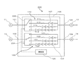
- FIG. 1 is a block diagram showing the configuration of the delay control device 100 of the present embodiment
- FIG. 2 is a diagram for changing the relative delay time between two signals from the outside using the delay control device 100 of the present embodiment. It is a block diagram which shows an example of the system comprised so that it was possible.
- the delay control apparatus 100 of this embodiment includes a first input terminal 101 and a second input terminal 102 for inputting an input pulse signal from the outside, and two inputs input from the first input terminal 101 and the second input terminal 102.
- a delay control circuit 105 that outputs a signal after delaying the signal by a predetermined delay time, a control unit 106 that outputs a control signal for controlling the delay time to the delay control circuit 105, and an output signal from the delay control circuit 105 Is provided with a first output terminal 103 and a second output terminal 104.
- the first input pulse signal 11 and the second input pulse signal 12 are input to the first input terminal 101 and the second input terminal 102, respectively, as input signals, and the first output terminal is used as an output signal.
- the first output pulse signal 13 and the second output pulse signal 14 are output from the 103 and the second output terminal 104, respectively.
- the first input pulse signal 11 and the second input pulse signal 12 can be pulse signals having a pulse width of 1 ns, for example.
- the relative delay time between the first output pulse signal 13 and the second output pulse signal 14 is calculated using an external arithmetic processing device (in FIG. 2, a personal computer). (PC)) It can be changed from 1. That is, the target value of the delay time is input from the arithmetic processing unit 1 to the control unit 106, and the control unit 106 controls the delay control circuit 105 so that the relative relationship between the first output pulse signal 13 and the second output pulse signal 14 is controlled.
- PC personal computer
- a value close to the target value preferably a value close to the third within the target value, more preferably a value close to the second, and more preferably a value closest to the target value (including values that match the target value) .
- the delay control circuit 105 corresponds to the two input pulse signals 11 and 12, the two signal path parts of the first signal path part 110 and the second signal path part 120, the first output side switch 131 and the second output. Two output side switches of the side switch 132 are provided.
- the first input pulse signal 11 is input from the first input terminal 101 to the first signal path unit 110, and further output from the first output terminal 103 via the first output side switch 131.
- the second input pulse signal 12 is input from the second input terminal 102 to the second signal path unit 120 and further output from the second output terminal 104 via the second output side switch 132.
- the first signal path unit 110 includes four signal paths 111 to 114 obtained by branching the path from the first input terminal 101 into four, and each output side is connected to the first output side switch 131. Different zero or even number of NOT gates 107 are cascade-connected to the signal paths 111 to 114.
- the second signal path unit 120 includes four signal paths 121 to 124 obtained by branching the path from the second input end 102 into four, and each output side is connected to the second output side switch 132. ing. Different zero or even number of NOT gates 107 are cascade-connected to the signal paths 121 to 124.
- the signal paths 111 to 114 and the signal paths 121 to 124 are each provided with 0 or an even number of NOT gates 107 in order to prevent the input pulse signal from being inverted.
- One NOT gate 107 inverts an input signal and outputs it after being delayed by a predetermined time. Therefore, in this embodiment, the input pulse signals 11 and 12 are configured to pass through 0 or an even number of NOT gates 107.
- NOT gates 107 are connected in cascade to signal paths 111 to 114, 0, 2, 4, and 6, respectively, and 0, 2, 4, and 6 are connected to signal paths 121 to 124, respectively. It is connected.
- the first output-side switch 131 selects any one of the terminals connected to the four signal paths 111 to 114 and connects it to the terminal connected to the first output terminal 103.
- the first input pulse signal 11 is output from the first input terminal 101 to the first output terminal 103 via any one of the signal paths 111 to 114.
- the second output switch 132 selects any one of the terminals connected to the four signal paths 121 to 124 and connects the selected terminal to the terminal connected to the second output terminal 104.
- the second input pulse signal 12 is output from the second input terminal 102 to the second output terminal 104 via any one of the signal paths 121 to 124.
- the NOT gate 107 cascaded inside the first signal path unit 110 and the second signal path unit 120 delays a signal passing therethrough by a predetermined delay time (gate delay) and outputs the delayed signal. Therefore, by changing the number of NOT gates 107 connected in cascade to each of the signal paths 111 to 114 and 121 to 124, the signal paths 111 to 114 and 121 to 124 can be configured to have different delay times. .
- the delay time given by the route selection from the signal paths 111 to 114 and 121 to 124 is influenced not only by the number of the NOT gates 107 but also by the wiring position where each signal path is formed. As a result, even between signal paths having the same number of NOT gates 107, the delay time differs because the wiring paths are different.
- the delay control apparatus 100 includes any one of the four signal paths 111 to 114 of the first signal path unit 110 and the four signal paths 121 to 124 of the second signal path unit 120, each having a different delay time. By combining any one of them, the relative delay time between two input pulse signals can be finely changed.
- the control unit 106 controls the first output side switch 131 and the second output side switch 132 to be appropriately switched when, for example, the target value of the delay time is input from the external arithmetic processing device 1.
- the control unit 106 appropriately switches the first output side switch 131 and the second output side switch 132, the signal path of the first signal path unit 110 through which the first input pulse signal 11 passes and the second input pulse signal 12 are changed.
- the signal path of the second signal path unit 120 that passes is selected.
- the delay time when the first input pulse signal 11 passes through the first signal path unit 110 and the delay time when the second input pulse signal 12 passes through the second signal path unit 120 change. Thereby, a value close to the target value can be selected as a relative delay time between the first output pulse signal 13 and the second output pulse signal 14.
- the target value of the delay time is set to the control unit 106 from the external processing unit 1.
- the delay time target value setting procedure or the like is determined in advance, the target value is set. It is also possible to program the setting procedure and have the control unit 106 have it in advance.
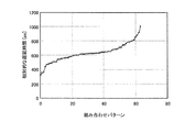
- An example of the relative delay time between the first output pulse signal 13 and the second output pulse signal 14 for each combination is shown in Table 1.
- FIG. 3 shows a plot of the results shown in Table 1 arranged in order from a combination with a short delay time.
- the delay control apparatus 100 selects two signal paths one by one from the first signal path unit 110 and the second signal path unit 120 having two or more signal paths.
- the relative delay time between two signals can be finely controlled.
- a value close to a predetermined target value can be selected as a relative delay time between the first output pulse signal 13 and the second output pulse signal 14.
- the delay control apparatus 100 of the present embodiment can be realized using, for example, a PLD (Programmable Logic Device).
- PLD Process-Demand Device
- the delay control device 100 can be reduced in size and cost can be reduced.
- the delay control device 100 of the present embodiment as shown in Table 1 and FIG. 3, the delay time can be controlled in ps order.
- the first signal path unit 110 and the second signal path unit 120 are each configured to have four signal paths.
- the present invention is not limited to this, and two or more signals each. What is necessary is just to comprise so that it may have a path
- the first signal path unit 110 and the second signal path unit 120 do not necessarily have the same number of signal paths. As the number of combinations of the signal path of the first signal path unit 110 and the signal path of the second signal path unit 120 increases, the relative delay time between the first output pulse signal 13 and the second output pulse signal 14 is increased. It becomes possible to select more finely.
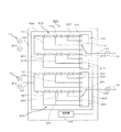
- FIG. 4 is a block diagram showing a configuration of the delay control apparatus 200 of the present embodiment.
- the delay control device 200 of the present embodiment replaces the first output side switch 131 and the second output side switch 132 included in the delay control device 100 of the first embodiment, and includes a first input side switch 233 and a second input side switch. 234.
- the first input pulse signal 11 is sent to the first output terminal via any one of the four signal paths 111 to 114 of the first signal path unit 110 selected by the first input side switch 233.
- the second input pulse signal 12 is sent to the second output terminal via one of the four signal paths 121 to 124 of the second signal path unit 120 selected by the second input side switch 234.
- 104 is output.
- 0, 2, 4, and 6 NOT gates 107 are cascade-connected to each of the signal paths 111 to 114, and similarly, 0 to each of the signal paths 121 to 124. Two, four, and six NOT gates 107 are connected in cascade.
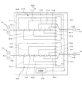
- FIG. 5 is a block diagram illustrating a configuration of the delay control apparatus 300 according to the present embodiment.
- the delay control device 300 of this embodiment includes a first output switch 131 and a second output switch 132 included in the delay control device 100 of the first embodiment, and a first input included in the delay control device 200 of the second embodiment. Both the side switch 233 and the second input side switch 234 are provided.
- the control unit 106 performs control so that the input signal switch 233 and the output switch 131 and the input switch 234 and the output switch 132 select the same signal path.
- the first input pulse signal 11 passes through any one of the four signal paths 111 to 114 of the first signal path unit 110 selected by the first input side switch 233. It is transmitted to the first output side switch 131. Also in the first output side switch 131, the same signal path as the signal path selected by the first input side switch 233 is selected, and the first input pulse signal 11 passes through the first output side switch 131 and outputs the first output. Output to the end 103.
- the second input pulse signal 12 also has one of the four signal paths 121 to 124 of the second signal path unit 120 selected by the second input side switch 234 and the second output side switch 132. Via the second output terminal 104.
- the delay control apparatus 300 also combines the selection by the first input side switch 233 and the first output side switch 131 with the selection by the second input side switch 234 and the second output side switch 132. It is possible to provide 16 different delay times. As a result, similar to the delay control device 100 of the first embodiment, a value close to the target value can be selected as the delay time. In addition, by implementing the delay control device 300 of the present embodiment using a PLD, it is possible to reduce the size and reduce the cost.
- FIG. 6 is a block diagram illustrating a configuration of the delay control device 400 of the present embodiment.
- a delay control circuit 405 having a different configuration is used instead of the delay control circuit 105 used in the first embodiment. That is, the first signal path unit 410, the second signal path unit 420, the first output side switch 431, and the second output side switch 432 included in the delay control circuit 405 of the present embodiment are the same as those used in the first embodiment.
- the configuration is different from the one signal path unit 110, the second signal path unit 120, the first output side switch 131, and the second output side switch 132.
- 0 or an even number of NOT gates 107 are cascade-connected to the signal paths 111 to 114 and the signal paths 121 to 124, respectively.
- the number of connections of the NOT gate 107 is limited to an even number, the number of signal paths in which the number of connections of the NOT gate 107 is different in each of the first signal path unit 110 and the second signal path unit 120 is limited. It was.
- four signal paths are provided in each of the first signal path unit 110 and the second signal path unit 120, and the number of combinations of selection of each signal path is 16.
- an odd number of NOT gates 107 can be connected to one signal path.
- an inverted input pulse signal is passed through a signal path that cascades an odd number of NOT gates 107.
- both the non-inverted signal and the inverted signal are used as the input pulse signal.
- the first signal path unit 410 used in the present embodiment is in addition to the first sub signal path unit including signal paths 111 to 114 in which NOT gates 107 are cascade-connected with an even number of 0, 2, 4, and 6.
- the second sub-signal path section is formed of signal paths 411 to 414 in which NOT gates 107 are connected in an odd number of one, three, five, and seven.
- the first signal path unit 410 has eight signal paths with different numbers of cascaded NOT gates 107.
- the second signal path section 420 also includes a third sub signal path section including signal paths 121 to 124 in which 0, 2, 4, and 6 NOT gates 107 are connected in cascade, and one NOT gate 107.
- a fourth sub-signal path section composed of three, five, and seven cascaded signal paths 421 to 424, and eight signal paths with different numbers of NOT gates 107.
- each of the first output side switch 431 and the second output side switch 432 has eight. Terminal.
- the control unit 106 since the non-inverted signal or the inverted signal is input to the first input terminal 101 and the second input terminal 102 as the first input pulse signal 11 and the second input pulse signal 12, the control unit 106 The control of the first output side switch 431 and the second output side switch 432 is changed depending on whether the input pulse signal is a non-inverted signal or an inverted signal. That is, when the first input pulse signal 11 is a non-inverted signal, the control unit 106 connects the first output-side switch 431 to any one of the signal paths 111 to 114 of the first sub signal path unit. When the first input pulse signal 11 is an inverted signal, the first output-side switch 431 is controlled to be connected to any one of the signal paths 411 to 414 of the second sub signal path unit.
- the control unit 106 connects the second output-side switch 432 to any one of the signal paths 121 to 124 of the third sub-signal path unit,
- the second output side switch 432 is connected to any one of the signal paths 421 to 424 of the fourth sub signal path section.
- FIG. 7 shows a plot of the results shown in Table 2 arranged in order from a combination with a short delay time.
- the delay control device 400 of this embodiment can realize the delay time more finely as shown in FIG. .
- a desired delay time can be realized with high accuracy, and distance measurement to an object can be performed with high accuracy.
- the delay control device 400 of the present embodiment more NOT gates 107 are used than in the first to third embodiments, but this can also be realized using a PLD.
- the PLD the delay control device 400 can be reduced in size and cost can be reduced.
- FIG. 8 is a block diagram showing the configuration of the delay control device 500 of this embodiment.
- the delay control device 500 according to the present embodiment replaces the first output side switch 431 and the second output side switch 432 included in the delay control device 400 according to the fourth embodiment, and includes a first input side switch 533 and a second input side switch. 534.
- the first input side switch 533 is one of the signal paths 111 to 114 of the first sub signal path section when the first input pulse signal 11 is a non-inverted signal among the eight signal paths of the first signal path section 410.
- any one is selected, and when the first input pulse signal 11 is an inverted signal, any one of the signal paths 411 to 414 of the second sub-signal path section is selected.
- the first input pulse signal 11 is output from the first input terminal 101 to the first output terminal 103 via the signal path selected by the first input side switch 533 in the first signal path unit 410.
- the second input-side switch 534 includes the signal paths 121 to 124 of the third sub-signal path section when the second input pulse signal 12 is a non-inverted signal among the eight signal paths of the second signal path section 420. Or any one of the signal paths 421 to 424 of the fourth sub-signal path section is selected when the second input pulse signal 12 is an inverted signal.
- the second input pulse signal 12 is output from the second input terminal 102 to the second output terminal 104 via the signal path selected by the second input side switch 534 in the second signal path unit 420.
- the first signal path unit 410 and the second signal path unit 420 have 8 signal paths each having 0 to 7 NOT gates 107, and are selected by the first input side switch 533.
- the delay control device 500 of this embodiment can provide 64 different delay times. As a result, similarly to the delay control device 400 of the fourth embodiment, the delay time can be realized more finely.
- the delay control device 500 of this embodiment using a PLD, it is possible to reduce the size and reduce the cost.
- FIG. 9 is a block diagram showing the configuration of the delay control device 600 of this embodiment.
- the delay control device 600 of the present embodiment includes a first output switch 431 and a second output switch 432 included in the delay control device 400 of the fourth embodiment, and a first input included in the delay control device 500 of the fifth embodiment. Both the side switch 533 and the second input side switch 534 are provided.
- the control unit 106 performs control so that the same path is selected by the input side switch and the output side switch.
- the first input pulse signal 11 is one of the eight signal paths 111 to 114 and 411 to 414 of the first signal path unit 410 selected by the first input side switch 533.
- the first output side switch 431 To the first output side switch 431. Also in the first output side switch 431, the same signal path as that selected by the first input side switch 533 is selected, and the first input pulse signal 11 passes through the first output side switch 431 and passes through the first output terminal. 103.
- the second input pulse signal 12 is selected from the eight signal paths 121 to 124 and 421 to 424 of the second signal path unit 420 by the second input side switch 534 and the second output side switch 432. Is output to the second output terminal 104 via one of them.
- the first signal path unit 410 and the second signal path unit 420 have eight signal paths each having 0 to 7 NOT gates 107, and the first input side switch 533 and the first signal path unit 533
- the delay control device 600 of this embodiment can provide 64 different delay times. Become.
- the delay time can be realized more finely.
- the delay control device 600 of the present embodiment using a PLD, it is possible to reduce the size and reduce the cost.
- the first signal path 110 and the second signal path section 120 have a plurality of signal paths in which 0 or even number of NOT gates are connected in cascade.
- the first signal path section 410 and the second signal path section 420 are each composed of a plurality of signal paths in which different 0 or even number of NOT gates are connected in cascade.
- a sub-signal path section (first and third sub-signal path sections) and a sub-signal path section (second and fourth sub-signal path sections) comprising a plurality of signal paths in which different odd number of NOT gates are connected in cascade.
- the present invention is not limited to this, and (C) a plurality of signal paths obtained by cascading 0 or even number of NOT gates in which either one of the first signal path section and the second signal path section is different.
- a sub-signal path section having only one of a plurality of signal paths in which different odd-numbered NOT gates are cascade-connected, and the other is a plurality of signal paths in which different 0 or even-numbered NOT gates are cascade-connected
- First or third sub-signal path section and a sub-signal path section (second or fourth sub-signal path section) composed of a plurality of signal paths in which different odd number of NOT gates are connected in cascade.
- one of the first signal path section and the second signal path section has one of the first or third sub signal path section and the second or fourth sub signal path section;
- First signal path and second signal path The other is also applicable to a case of having a first or third sub-signal path portion and the other of the second or fourth sub-signal path of the.
- the number of NOT gates provided in each signal path in the first signal path section and the second signal path section is different, but it is formed in, for example, a PLD. If the delay time of each signal path is different due to the influence of the wiring position and the like, the number of NOT gates may be the same. Further, if the delay time of each signal path is different due to the influence of the wiring position formed in the PLD, the NOT gate is not necessarily used.
- FIG. 13 is a block diagram showing the configuration of the delay control device 700 of this embodiment.
- the delay control device 700 of this embodiment is configured to realize a delay time comparable to that of the delay control device 100 of the first embodiment using a small number of NOT gates 107.
- the first signal path unit 110 and the second signal path unit 120 each include four signal paths, and each of the signal paths has 0, 2, 4, 6 (different 0). Or even number) NOT gates 107 are connected in cascade. As a result, each of the first signal path unit 110 and the second signal path unit 120 requires twelve NOT gates 107.
- the first signal path unit 710 and the second signal path unit 720 are each configured by using six NOT gates 107.
- the first signal path unit 710 six NOT gates 107 are connected in cascade to form a signal path 714, and signal paths 711 to 713 are branched from the middle of the signal path 714. That is, the signal path 711 is branched from the signal path 714 and connected to the first output side switch 131 before passing through the NOT gate 107 after being input from the first input terminal 101.
- the signal path 712 is branched from the signal path 714 at a point where the two NOT gates 107 are passed and connected to the first output side switch 131.
- the signal path 713 is branched from the signal path 714 at a point where it passes through the four NOT gates 107 and connected to the first output side switch 131.
- the first signal path section 710 having signal paths 711 to 714 that pass through 0, 2, 4, and 6 NOT gates 107 can be formed.
- the delay control device 700 according to the present embodiment uses half the number of NOT gates 107 as the delay control device 100 according to the first embodiment.
- the relative delay time between the signal 13 and the second output pulse signal 14 can be realized to the same extent as in the first embodiment.
- route part 720 of this embodiment are applicable also to the structure of 2nd Embodiment. That is, as in the second embodiment, the first input side switch 233 and the second input side switch 234 are provided, and one terminal at one connection end of the first input side switch 233 (second input side switch 234) A signal path 714 (signal path 724) in which six NOT gates 107 are cascade-connected is disposed between the first output terminal 103 (second output terminal 104) and a first input side switch 233 (second input side).
- the signal path exiting from the other terminal of one connection end of the switch 234) is a point that has passed two NOT gates on the signal path 714 (signal path 724), a point that has passed four NOT gates, and six points.
- the signal path 714 (signal path 724) may be merged at a point that passes through the NOT gate.
- FIG. 14 is a block diagram showing the configuration of the delay control apparatus 800 of this embodiment.
- the delay control device 800 of the present embodiment is configured to realize a delay time comparable to that of the delay control device 400 of the fourth embodiment using a small number of NOT gates 107.
- the first signal path unit 810 of the present embodiment includes a first sub signal path unit in which signal paths 711 to 714 similar to the first signal path unit 710 of the seventh embodiment are formed using six NOT gates 107.
- the second sub signal path portion is formed of signal paths 811 to 814 using seven NOT gates 107.
- the second sub signal path section of the first signal path section 810 forms a signal path 814 by cascading seven NOT gates 107, and branches signal paths 811 to 813 from the middle of the signal path 814. . That is, the signal path 811 is branched from the signal path 814 at a point where the signal path 811 passes through one NOT gate 107 after being input from the first input terminal 101, and is connected to the first output side switch 431. The signal path 812 is branched from the signal path 814 at a point where it passes through the three NOT gates 107 and connected to the first output side switch 431. Further, the signal path 813 is branched from the signal path 814 at a point where it has passed through the five NOT gates 107 and connected to the first output side switch 431.
- the second sub signal path portion of the first signal path portion 810 having signal paths 811 to 814 that pass 1, 3, 5, and 7 can be formed.
- the second signal path unit 820 has the same configuration.
- the delay control device 800 of the present embodiment uses the NOT gates 107 that are less than half the number of the delay control devices 400 of the fourth embodiment to generate the first output pulse signal 13 and the second output pulse signal 14.
- the relative delay time can be realized to the same extent as in the fourth embodiment.
- route part 820 of this embodiment are applicable also to the structure (FIG. 8) of 5th Embodiment. That is, as in the fifth embodiment, the first input side switch 533 and the second input side switch 534 are provided.
- the first signal path unit 810 a signal path 714 in which six NOT gates 107 are cascade-connected between one terminal of one connection end of the first input side switch 533 and the first output end 103.
- a signal path that exits from the other terminal of one of the connection ends of the first input side switch 533 is a point that has passed two NOT gates on the signal path 714 and a point that has passed four NOT gates.
- the signal path 714 is merged at the point where the six NOT gates are passed.
- a signal path 814 in which seven NOT gates 107 are cascade-connected is arranged between the other terminal of one connection end of the first input side switch 533 and the first output end 103, and the first input
- the signal path that exits from the other terminal of one connection end of the side switch 533 passes through the two NOT gates on the signal path 814, passes through the four NOT gates, and passes through the six NOT gates.
- the signal path 814 is joined at the point where Similarly, for the second signal path unit 820, a signal path 724 in which six NOT gates 107 are connected in cascade and a signal path 824 in which seven NOT gates 107 are connected in cascade are connected to the second input side switch 534. It is arranged between the second output terminals 104.
- FIG. 15 is a block diagram showing the configuration of the delay control device 900 of this embodiment.
- the delay control device 900 according to the present embodiment is configured to achieve a delay time comparable to that of the delay control device 400 according to the fourth embodiment using a smaller number of NOT gates 107 than the eighth embodiment. It is a thing.
- a plurality of (seven in this embodiment) NOT gates 107 are connected in cascade to form a signal path 814 (first main signal path), and an odd number of NOT gates of these seven NOT gates.
- the signal path is branched before entering the first, third, fifth, and seventh NOT gates 107 to form signal paths 711, 712, 713, and 714, and even-numbered NOT gates
- the signal path is branched to form signal paths 811, 812, 813.
- the signal paths 711, 712, 713, and 714 pass through different 0 or even number (0, 2, 4, and 6 respectively) of NOT gates 7 and constitute a first sub signal path section.
- the signal paths 811, 812, 813, and 814 pass through different odd numbers (one, three, five, and seven, respectively) of NOT gates 107 to form a second sub signal path section.
- the second signal path unit 920 is configured by branching a signal path 824 (second main signal path) in which a plurality of NOT gates 107 are connected in cascade.
- the delay control device 900 uses a smaller number of NOT gates 107 than the delay control device 800 according to the eighth embodiment, so that the relative relationship between the first output pulse signal 13 and the second output pulse signal 14 is relatively small.
- the delay time can be realized to the same extent as in the fourth embodiment.
- route part 920 of this embodiment are applicable also to the structure of 5th Embodiment. That is, as in the fifth embodiment, it is possible to connect the first input side switch 533 and the second input side switch 534 to the input side of the first signal path unit 910 and the second signal path unit 920, respectively. .
- the description in the present embodiment shows an example of the delay control device according to the present invention, and the present invention is not limited to this.
- the detailed configuration and detailed operation of the delay control device in the present embodiment can be changed as appropriate without departing from the spirit of the present invention.
Abstract
2つの信号間の相対的な遅延時間を制御する小型化容易な遅延制御装置を提供する。第1信号経路部110及び第2信号経路部120のそれぞれの信号経路111~114及び信号経路121~124は、それぞれ遅延時間が異なっている。第1信号経路部110の4つの信号経路111~114のいずれか1つと第2信号経路部120の4つの信号経路121~124のいずれか1つとを選択することで、2つの入力パルス信号間の相対的な遅延時間をきめ細かく変更することが可能となる。
Description
本発明は、例えばUWB(Ultra Wideband)レーダにおけるパルス信号の送受信間の遅延時間を微小な時間単位で制御する遅延制御装置に関するものである。
パルス信号を用いたUWBレーダ装置では、パルス状の送信信号を送信してから受信信号を検波するまでの遅延時間を制御することで、所定の距離範囲内にある対象物を検出している。具体的には、検出範囲である所定の距離を複数個の距離ゲートに分割し、複数の距離ゲートのそれぞれの受信信号の強度から対象物が存在する距離ゲートを検出している。距離ゲート毎に受信信号の強度を測定するためには、距離ゲートに対応した送信信号と受信信号との間の相対的な遅延時間を高精度に制御する必要がある。
遅延時間を制御する従来の遅延時間制御回路として、例えば特許文献1に記載のものが知られている。特許文献1の遅延回路は、図10に示すように、MOS型トランジスタを利用したNMOSトランジスタTRnと、このNMOSトランジスタTRnと直列に接続したコンデンサCとから構成され、入力信号を所定時間だけ遅延させて出力する。遅延回路900の入力側、出力側のそれぞれにNOTゲートのNOTin、NOToutが接続されている。
NMOSトランジスタTRnは、そのドレイン端子がNOTゲートNOTinとNOToutとを結ぶ入出力信号側に接続され、ソース端子がコンデンサCを介して電源側のグランドに接続され、ゲート端子は電源電圧(Vcc)に固定されて常にオン状態に設定されている。ここでは、NMOSトランジスタTRnがゲートーソース間電圧を制御可能な可変抵抗Rとして利用される。この可変抵抗Rによる抵抗値とコンデンサCによる容量値により遅延量を決定することができる。図11に示すようなパルス電圧Vinが入力されると、接続点における電圧Vpが積分波形となり、入力のパルス電圧に対してCRの時定数による遅延時間tdだけ遅延されたパルス電圧Voutが出力される。
また、別の従来の遅延回路として、特許文献2に記載のものも知られている。特許文献2に記載の可変遅延回路は、図12に示すように、入力端子921に入力した信号をそれぞれ出力端子922に送る2つの経路A、Bと、セレクト信号により経路A,Bを切り替える選択部を備える可変遅延部924と、それぞれの経路A,Bの少なくとも一部の遅延時間のx倍、y倍の発振周期を持つリング発振器925、929と、それぞれ第1クロック信号とリング発振器925の出力、第2クロック信号とリング発振器929の出力の位相を比較する位相比較回路927、931と、それぞれ位相比較回路927、931の位相比較結果からリング発振器925、929の発振周期が第1クロック信号、第2クロック信号の周期と等しくなるようにリング発振器925、929の発振周期を制御すると共に経路A,Bの遅延時間を制御する遅延時間制御回路928、932とを備えている。
経路Aはn個の可変遅延素子Taを介在し、経路Bはm個の可変遅延素子Tbを介在する。リング発振器925は経路Aと同一の可変遅延素子Taをx´個直列に接続して、その出力を反転して入力側に帰還して構成し、遅延時間制御回路928は経路Aの可変遅延素子Ta及びリング発振器925の各可変遅延素子Taの遅延時間を同時に制御する。リング発振器929は経路Bと同一の可変遅延素子Tbをy´個(第1クロック信号の周期をT1、第2クロック信号の周期をT2としたとき、T1×x´/n≠T2×y´/m)個直列に接続して、その出力を反転して入力側に帰還して構成し、遅延時間制御回路932は経路Bの可変遅延素子Tb及びリング発振器929の各可変遅延素子Tbの遅延時間を同時に制御する。上記構成の可変遅延回路920では、第1の経路Aの遅延時間がT1/y、第2の経路Bの遅延時間がT2/yとなり、T1、T2、x、yの値を適当なものに定めることにより、所望する任意の分解能を選択できる。
上記の特許文献1に記載の遅延回路900や特許文献2に記載の可変遅延回路920では、1つの入力信号に対して遅延時間を与える構成となっている。このような遅延回路をレーダ装置に用いて対象物までの距離等を測定するためには、送信信号と受信信号の少なくとも一方に遅延時間を与えるように構成することで、送信信号と受信信号との間の相対的な遅延時間を制御できるようにする必要がある。
しかしながら、特許文献1に記載の遅延回路では、実装時はすべての回路が固定されてしまうため、実装後に回路内部を変更して遅延時間を再調整することが困難になる。そのため、送信信号と受信信号との間の相対的な遅延時間を順次変更していく必要のあるレーダ装置に用いることはできない。また、特許文献2に記載の可変遅延回路では、実装後に遅延時間を変更することは可能なものの、可変遅延回路が大規模となって大きな設置面積が必要となり、また高コストになるといった問題もある。従って、小型化が要求されるUWBレーダに用いることはできない。
本発明は、上記課題に鑑みてなされたものであり、2つの信号間の相対的な遅延時間を制御する小型化が容易な遅延制御装置を提供することを目的とする。
上記課題を解決するため、本発明の遅延制御装置の第1の態様は、第1入力パルス信号と第2入力パルス信号とを入力し、相対的な遅延時間が所定の目標値に近い第1出力パルス信号と第2出力パルス信号とを出力する遅延制御装置であって、前記第1入力パルス信号を入力する第1入力端と、前記第2入力パルス信号を入力する第2入力端と、前記第1出力パルス信号を出力する第1出力端と、前記第2出力パルス信号を出力する第2出力端と、遅延時間の異なる信号経路を2以上有する第1信号経路部と、遅延時間の異なる信号経路を2以上有する第2信号経路部と、前記第1信号経路部の2以上の信号経路のそれぞれの一端を接続する2以上の端子からなる一方の接続端と1端子からなる他方の接続端とを有する第1スイッチと、前記第2信号経路部の2以上の信号経路のそれぞれの一端を接続する2以上の端子からなる一方の接続端と1端子からなる他方の接続端とを有する第2スイッチと、前記第1出力パルス信号と前記第2出力パルス信号との間の相対的な遅延時間が前記目標値に近くなるように、前記第1スイッチの前記一方の接続端のいずれか1つの端子を選択して前記第1スイッチの前記他方の接続端の端子に接続させるとともに、前記第2スイッチの前記一方の接続端のいずれか1つの端子を選択して前記第2スイッチの前記他方の接続端の端子に接続させるための制御信号を前記第1スイッチ及び前記第2スイッチにそれぞれ出力する制御部と、を備え、前記第1信号経路部と前記第1スイッチとが前記第1入力端と前記第1出力端との間に接続され、前記第2信号経路部と前記第2スイッチとが前記第2入力端と前記第2出力端との間に接続されていることを特徴とする。
本発明の第1の態様によれば、2つの信号間の相対的な遅延時間を高精度に制御することができる。
本発明の遅延制御装置の他の態様は、前記第1信号経路部および/または第2信号経路部の信号経路は、0または1個以上の縦続接続されたNOTゲートを信号経路上に設けることにより、前記遅延時間が各信号経路間で異なるように構成されていることを特徴とする。
本発明の遅延制御装置の他の態様は、前記制御部は、前記第1入力パルス信号が非反転信号であるか反転信号であるかに応じて、それぞれ、前記第1スイッチを前記第1信号経路部の中の0または偶数個のNOTゲートを通過する信号経路の一つ又は奇数個のNOTゲートを通過する信号経路の一つに接続するとともに、前記第2入力パルス信号が非反転信号であるか反転信号であるかに応じて、それぞれ、前記第2スイッチを前記第2信号経路部の中の0または偶数個のNOTゲートを通過する信号経路の一つ又は奇数個のNOTゲートを通過する信号経路の一つに接続する。
本発明の遅延制御装置の他の態様は、前記第1信号経路部の2以上の信号経路は、それぞれの出力側が前記第1スイッチの前記一方の接続端に接続され、入力側が合流されて前記第1入力端に接続され、前記第1スイッチの前記他方の接続端が前記第1出力端に接続され、前記第2信号経路部の2以上の信号経路は、それぞれの出力側が前記第2スイッチの前記一方の接続端に接続され、入力側が合流されて前記第2入力端に接続され、前記第2スイッチの前記他方の接続端が前記第2出力端に接続されていることを特徴とする。
本発明の遅延制御装置の他の態様は、前記第1スイッチの前記他方の接続端が前記第1入力端に接続され、前記第1信号経路部の2以上の信号経路は、それぞれの入力側が前記第1スイッチの前記一方の接続端に接続されるとともに出力側が合流されて前記第1出力端に接続され、前記第2スイッチの前記他方の接続端が前記第2入力端に接続され、前記第2信号経路部の2以上の信号経路は、それぞれの入力側が前記第2スイッチの前記一方の接続端に接続されるとともに出力側が合流されて前記第2出力端に接続されていることを特徴とする。
本発明の遅延制御装置の他の態様は、前記第1スイッチ及び前記第2スイッチを2つずつ設けてそれぞれを前記第1信号経路部の入力側と出力側及び前記第2信号経路部の入力側と出力側に接続し、前記第1信号経路部の入力側に接続された前記第1スイッチの前記他方の接続端が前記第1入力端に接続されるとともに前記第1信号経路部の出力側に接続された前記第1スイッチの前記他方の接続端が前記第1出力端に接続され、前記第2信号経路部の入力側に接続された前記第2スイッチの前記他方の接続端が前記第2入力端に接続されるとともに前記第2信号経路部の出力側に接続された前記第2スイッチの前記他方の接続端が前記第2出力端に接続されていることを特徴とする。
本発明の遅延制御装置の他の態様は、前記第1入力パルス信号は非反転信号であり、前記第1信号経路部は、前記2以上の信号経路のそれぞれが、異なる0または偶数個のNOTゲートを通過するように構成されていることを特徴とする。
本発明の遅延制御装置の他の態様は、前記第1入力パルス信号は反転信号であり、前記第1信号経路部は、前記2以上の信号経路のそれぞれが、異なる奇数個のNOTゲートを通過するように構成されていることを特徴とする。
本発明の遅延制御装置の他の態様は、前記第1入力パルス信号は非反転信号または反転信号であり、前記第1信号経路部は、それぞれ異なる0または偶数個のNOTゲートを通過する2以上の信号経路からなる第1サブ信号経路部と、それぞれ異なる奇数個のNOTゲートを通過する2以上の信号経路からなる第2サブ信号経路部とを有しており、前記制御部は、前記第1入力パルス信号が非反転信号のときは、前記第1サブ信号経路部の中の1つの信号経路を選択させる制御信号を前記第1スイッチに出力し、前記第1入力パルス信号が反転信号のときは、前記第2サブ信号経路部の中の1つの信号経路を選択させる制御信号を前記第1スイッチに出力することを特徴とする。
本発明の遅延制御装置の他の態様は、前記第2入力パルス信号は非反転信号であり、前記第2信号経路部は、前記2以上の信号経路のそれぞれが、異なる0または偶数個のNOTゲートを通過するように構成されていることを特徴とする。
本発明の遅延制御装置の他の態様は、前記第2入力パルス信号は反転信号であり、前記第2信号経路部は、前記2以上の信号経路のそれぞれが、異なる奇数個のNOTゲートを通過するように構成されていることを特徴とする。
本発明の遅延制御装置の他の態様は、前記第2入力パルス信号は非反転信号または反転信号であり、前記第2信号経路部は、それぞれ異なる0または偶数個のNOTゲートを通過する2以上の信号経路からなる第3サブ信号経路部と、それぞれ異なる奇数個のNOTゲートを通過する2以上の信号経路からなる第4サブ信号経路部とを有しており、前記制御部は、前記第2入力パルス信号が非反転信号のときは、前記第3サブ信号経路部の中の1つの信号経路を選択させる制御信号を前記第2スイッチに出力し、前記第2入力パルス信号が反転信号のときは、前記第4サブ信号経路部の中の1つの信号経路を選択させる制御信号を前記第2スイッチに出力することを特徴とする。
本発明の遅延制御装置の他の態様は、前記第1入力パルス信号は非反転信号であり、前記第1信号経路部は、N1個(N1は2以上の偶数)のNOTゲートを縦続接続した第1主信号経路と、前記N1個のNOTゲートのうちのM1個目(M1=1,3,・・・,N1-1)の直前で前記第1主信号経路から分岐する分岐信号経路、または前記N1個のNOTゲートのうちのL1個目(L1=2,4,・・・,N1)の直後で前記第1主信号経路に合流する分岐信号経路とを有することを特徴とする。
本発明の遅延制御装置の他の態様は、前記第1入力パルス信号は反転信号であり、前記第1信号経路部は、N2個(N2は3以上の奇数)のNOTゲートを縦続接続した第2主信号経路と、前記N2個のNOTゲートのうちのM2個目(M2=1,3,・・・,N2-2)の直後で前記第2主信号経路から分岐する分岐信号経路、または前記N2個のNOTゲートのうちのL2個目(L2=2,4,・・・,N2-1)の直後で前記第2主信号経路に合流する分岐信号経路とを有することを特徴とする。
本発明の遅延制御装置の他の態様は、前記第1入力パルス信号は非反転信号または反転信号であり、前記第1信号経路部は、(1)N1個(N1は2以上の偶数)のNOTゲートを縦続接続した第1主信号経路と、前記N1個のNOTゲートのうちのM1個目(M1=1,3,・・・,N1-1)の直前で前記第1主信号経路から分岐する分岐信号経路、または前記N1個のNOTゲートのうちのL1個目(L1=2,4,・・・,N1)の直後で前記第1主信号経路に合流する分岐信号経路、からなる第1サブ信号経路部と、(2)N2個(N2は3以上の奇数)のNOTゲートを縦続接続した第2主信号経路と、前記N2個のNOTゲートのうちのM2個目(M2=1,3,・・・,N2-2)の直後で前記第2主信号経路から分岐する分岐信号経路、または前記N2個のNOTゲートのうちのL2個目(L2=2,4,・・・,N2-1)の直後で前記第2主信号経路に合流する分岐信号経路からなる第2サブ信号経路部とを有しており、前記制御部は、前記第1入力パルス信号が非反転信号のときは、前記第1サブ信号経路部の中の1つの信号経路を選択させる制御信号を前記第1スイッチに出力し、前記第1入力パルス信号が反転信号のときは、前記第2サブ信号経路部の中の1つの信号経路を選択させる制御信号を前記第1スイッチに出力することを特徴とする。
本発明の遅延制御装置の他の態様は、前記第2入力パルス信号は非反転信号であり、前記第2信号経路部は、N3個(N3は2以上の偶数)のNOTゲートを縦続接続した第3主信号経路と、前記N3個のNOTゲートのうちのM3個目(M3=1,3,・・・,N3-1)の直前で前記第3主信号経路から分岐する分岐信号経路、または前記N3個のNOTゲートのうちのL3個目(L3=2,4,・・・,N3)の直後で前記第3主信号経路に合流する分岐信号経路とを有することを特徴とする。
本発明の遅延制御装置の他の態様は、前記第2入力パルス信号は反転信号であり、前記第2信号経路部は、N4個(N4は3以上の奇数)のNOTゲートを縦続接続した第4主信号経路と、前記N4個のNOTゲートのうちのM4個目(M4=1,3,・・・,N4-2)の直後で前記第4主信号経路から分岐する分岐信号経路、または前記N4個のNOTゲートのうちのL4個目(L4=2,4,・・・,N4-1)の直後で前記第4主信号経路に合流する分岐信号経路とを有することを特徴とする。
本発明の遅延制御装置の他の態様は、前記第2入力パルス信号は非反転信号または反転信号であり、前記第2信号経路部は、(1)N3個(N3は2以上の偶数)のNOTゲートを縦続接続した第3主信号経路と、前記N3個のNOTゲートのうちのM3個目(M3=1,3,・・・,N3-1)の直前で前記第3主信号経路から分岐する分岐信号経路、または前記N3個のNOTゲートのうちのL3個目(L3=2,4,・・・,N3)の直後で前記第3主信号経路に合流する分岐信号経路、からなる第3サブ信号経路部と、(2)N4個(N4は3以上の奇数)のNOTゲートを縦続接続した第4主信号経路と、前記N4個のNOTゲートのうちのM4個目(M4=1,3,・・・,N4-2)の直後で前記第4主信号経路から分岐する分岐信号経路、または前記N4個のNOTゲートのうちのL4個目(L4=2,4,・・・,N4-1)の直後で前記第4主信号経路に合流する分岐信号経路からなる第4サブ信号経路部と、を有しており、前記制御部は、前記第2入力パルス信号が非反転信号のときは、前記第3サブ信号経路部の中の1つの信号経路を選択させる制御信号を前記第2スイッチに出力し、前記第2入力パルス信号が反転信号のときは、前記第4サブ信号経路部の中の1つの信号経路を選択させる制御信号を前記第2スイッチに出力することを特徴とする。
本発明の遅延制御装置の他の態様は、前記第1入力パルス信号は非反転信号または反転信号であり、前記第1信号経路部は、複数のNOTゲートを縦続接続した第1主信号経路を有するとともに、(1)前記第1主信号経路の途中から分岐しまたは前記第1主信号経路の全体を通過することにより、前記第1主信号経路の入力側から前記第1スイッチの前記一方の接続端までの間に異なる偶数個のNOTゲートを通過する複数の信号経路からなる第1サブ信号経路部と、前記第1主信号経路の途中から分岐しまたは前記第1主信号経路の全体を通過することにより、前記第1主信号経路の入力側から前記第1スイッチの前記一方の接続端までの間に異なる奇数個のNOTゲートを通過する複数の信号経路からなる第2サブ信号経路部、または、(2)前記第1主信号経路の途中から合流しまたは前記第1主信号経路の全体を通過することにより、前記第1スイッチの前記一方の接続端から前記第1主信号経路の出力側までの間に異なる偶数個のNOTゲートを通過する複数の信号経路からなる第1サブ信号経路部と、前記第1主信号経路の途中から合流しまたは前記第1主信号経路の全体を通過することにより、前記第1スイッチの前記一方の接続端から前記第1主信号経路の出力側までの間に異なる奇数個のNOTゲートを通過する複数の信号経路からなる第2サブ信号経路部、を有しており、前記制御部は、前記第1入力パルス信号が非反転信号のときは、前記第1サブ信号経路部の中の1つの信号経路を選択させる制御信号を前記第1スイッチに出力し、前記第1入力パルス信号が反転信号のときは、前記第2サブ信号経路部の中の1つの信号経路を選択させる制御信号を前記第1スイッチに出力することを特徴とする。
本発明の遅延制御装置の他の態様は、前記第2入力パルス信号は非反転信号または反転信号であり、前記第2信号経路部は、複数のNOTゲートを縦続接続した第2主信号経路を有するとともに、(1)前記第2主信号経路の途中から分岐しまたは前記第2主信号経路の全体を通過することにより、前記第2主信号経路の入力側から前記第2スイッチの前記一方の接続端までの間に異なる偶数個のNOTゲートを通過する複数の信号経路からなる第3サブ信号経路部と、前記第2主信号経路の途中から分岐しまたは前記第2主信号経路の全体を通過することにより、前記第2主信号経路の入力側から前記第2スイッチの前記一方の接続端までの間に異なる奇数個のNOTゲートを通過する複数の信号経路からなる第4サブ信号経路部、または、(2)前記第2主信号経路の途中から合流しまたは前記第2主信号経路の全体を通過することにより、前記第2スイッチの前記一方の接続端から前記第2主信号経路の出力側までの間に異なる偶数個のNOTゲートを通過する複数の信号経路からなる第3サブ信号経路部と、前記第2主信号経路の途中から合流しまたは前記第2主信号経路の全体を通過することにより、前記第2スイッチの前記一方の接続端から前記第2主信号経路の出力側までの間に異なる奇数個のNOTゲートを通過する複数の信号経路からなる第4サブ信号経路部、を有しており、前記制御部は、前記第2入力パルス信号が非反転信号のときは、前記第3サブ信号経路部の中の1つの信号経路を選択させる制御信号を前記第2スイッチに出力し、前記第2入力パルス信号が反転信号のときは、前記第4サブ信号経路部の中の1つの信号経路を選択させる制御信号を前記第2スイッチに出力することを特徴とする。
本発明の遅延制御装置の他の態様は、前記第1信号経路部、第2信号経路部、第1スイッチ、第2スイッチ、及び制御部が、PLD(Programmable Logic Device)内に構成されていることを特徴とする。
本発明によれば、2つの信号間の相対的な遅延時間を制御可能な小型化された遅延制御装置を提供することが可能となる。
本発明の好ましい実施の形態における遅延制御装置について、図面を参照して詳細に説明する。同一機能を有する各構成部については、図示及び説明簡略化のため、同一符号を付して示す。
(第1実施形態)
本発明の第1の実施形態に係る遅延制御装置を、図1、2を用いて以下に説明する。図1は、本実施形態の遅延制御装置100の構成を示すブロック図であり、図2は、本実施形態の遅延制御装置100を用いて2つの信号間の相対的な遅延時間を外部から変更可能に構成したシステムの一例を示すブロック図である。本実施形態の遅延制御装置100は、外部から入力パルス信号を入力するための第1入力端101及び第2入力端102と、第1入力端101及び第2入力端102から入力した2つの入力信号をそれぞれ所定の遅延時間だけ遅延させて出力する遅延制御回路105と、遅延制御回路105に対し遅延時間を制御するための制御信号を出力する制御部106と、遅延制御回路105からの出力信号を外部に出力するための第1出力端103及び第2出力端104とを備えている。
本発明の第1の実施形態に係る遅延制御装置を、図1、2を用いて以下に説明する。図1は、本実施形態の遅延制御装置100の構成を示すブロック図であり、図2は、本実施形態の遅延制御装置100を用いて2つの信号間の相対的な遅延時間を外部から変更可能に構成したシステムの一例を示すブロック図である。本実施形態の遅延制御装置100は、外部から入力パルス信号を入力するための第1入力端101及び第2入力端102と、第1入力端101及び第2入力端102から入力した2つの入力信号をそれぞれ所定の遅延時間だけ遅延させて出力する遅延制御回路105と、遅延制御回路105に対し遅延時間を制御するための制御信号を出力する制御部106と、遅延制御回路105からの出力信号を外部に出力するための第1出力端103及び第2出力端104とを備えている。
本実施形態の遅延制御装置100では、入力信号として第1入力パルス信号11及び第2入力パルス信号12がそれぞれ第1入力端101及び第2入力端102に入力され、出力信号として第1出力端103及び第2出力端104からそれぞれ第1出力パルス信号13及び第2出力パルス信号14が出力される。第1入力パルス信号11及び第2入力パルス信号12は、例えばパルス幅1nsのパルス信号とすることができる。
図2に示すシステムでは、第1出力パルス信号13と第2出力パルス信号14との間の相対的な遅延時間を、遅延制御装置100に接続された外部の演算処理装置(図2ではパーソナルコンピュータ(PC)としている)1から変更することができる構成としている。すなわち、演算処理装置1から制御部106に遅延時間の目標値を入力し、制御部106が遅延制御回路105を制御して第1出力パルス信号13と第2出力パルス信号14との間の相対的な遅延時間として上記の目標値に近い値(好ましくは目標値から3番目以内に近い値、さらに好ましくは2番目以内に近い値、さらに好ましくは最も近い値(目標値に一致する値を含む。)。以下同じ)を選択する。
遅延制御回路105は、2つの入力パルス信号11、12に対応させて、第1信号経路部110と第2信号経路部120の2つの信号経路部、及び第1出力側スイッチ131と第2出力側スイッチ132の2つの出力側スイッチを備えている。第1入力パルス信号11は、第1入力端101から第1信号経路部110に入力され、さらに第1出力側スイッチ131を経由して第1出力端103から出力される。同様に、第2入力パルス信号12は、第2入力端102から第2信号経路部120に入力され、さらに第2出力側スイッチ132を経由して第2出力端104から出力される。
第1信号経路部110は、第1入力端101からの経路を4つに分岐した4つの信号経路111~114を備えており、それぞれの出力側が第1出力側スイッチ131に接続されている。信号経路111~114には、異なる0または偶数個のNOTゲート107が縦続接続されている。同様に、第2信号経路部120は、第2入力端102からの経路を4つに分岐した4つの信号経路121~124を備えており、それぞれの出力側が第2出力側スイッチ132に接続されている。信号経路121~124には、異なる0または偶数個のNOTゲート107が縦続接続されている。
本実施形態では、信号経路111~114及び信号経路121~124のそれぞれに、NOTゲート107を0または偶数個備える構成としているが、これは入力パルス信号が反転しないようにするためである。1つのNOTゲート107は、入力信号を反転させ、かつ所定の時間だけ遅延させて出力する。そこで、本実施形態では、入力パルス信号11、12がNOTゲート107を0または偶数個通過するように構成している。図1では、NOTゲート107が、信号経路111~114にそれぞれ0個、2個、4個、6個縦続接続され、信号経路121~124にそれぞれ0個、2個、4個、6個縦続接続されている。
第1出力側スイッチ131は、4つの信号経路111~114にそれぞれ接続される端子のいずれか1つを選択して第1出力端103に接続された端子に接続する。これにより、第1入力パルス信号11は、第1入力端101から信号経路111~114のいずれか1つを経由して第1出力端103に出力される。また、第2出力側スイッチ132は、4つの信号経路121~124にそれぞれ接続される端子のいずれか1つを選択して第2出力端104に接続された端子に接続する。これにより、第2入力パルス信号12は、第2入力端102から信号経路121~124のいずれか1つを経由して第2出力端104に出力される。
第1信号経路部110及び第2信号経路部120の内部に縦続接続されているNOTゲート107は、これを通過する信号を所定の遅延時間だけ遅延(ゲート遅延)させて出力する。従って、信号経路111~114及び121~124のそれぞれに縦続接続させるNOTゲート107の個数を変えることで、信号経路111~114及び121~124のそれぞれで遅延時間が異なるように構成することができる。
また、信号経路111~114及び121~124からの経路選択によって与えられる遅延時間は、NOTゲート107の個数だけでなく、各信号経路が形成される配線位置等によっても影響を受ける。その結果、NOTゲート107の個数が等しい信号経路間でも、配線経路が異なるため遅延時間が異なってくる。本実施形態の遅延制御装置100は、それぞれで遅延時間の異なる第1信号経路部110の4つの信号経路111~114のいずれか1つと第2信号経路部120の4つの信号経路121~124のいずれか1つとを組み合わせることで、2つの入力パルス信号間の相対的な遅延時間をきめ細かく変更できるようにしている。
制御部106は、例えば外部の演算処理装置1から遅延時間の目標値を入力すると、第1出力側スイッチ131及び第2出力側スイッチ132を適切に切り替えるように制御する。制御部106が第1出力側スイッチ131及び第2出力側スイッチ132を適切に切り替えることで、第1入力パルス信号11が通過する第1信号経路部110の信号経路及び第2入力パルス信号12が通過する第2信号経路部120の信号経路が選択される。その結果、第1入力パルス信号11が第1信号経路部110を通過するときの遅延時間、及び第2入力パルス信号12が第2信号経路部120を通過するときの遅延時間がそれぞれ変化する。これにより、第1出力パルス信号13と第2出力パルス信号14との間の相対的な遅延時間として上記の目標値に近い値を選択することができる。
なお、図2では、遅延時間の目標値を外部の演算処理装置1から制御部106に設定する構成としているが、遅延時間目標値の設定手順等が事前に決まっている場合には、目標値の設定手順をプログラミング化して制御部106に事前に持たせるようにすることも可能である。
本実施形態の遅延制御装置100は、図1に示すように、第1信号経路部110が4つの信号経路111~114を有し、第2信号経路部120が4つの信号経路121~124を有する構成としていることから、第1出力側スイッチ131と第2出力側スイッチ132とで選択可能な信号経路の組み合わせ数は、4×4=16通りとなる。それぞれの組み合わせに対する第1出力パルス信号13と第2出力パルス信号14との間の相対的な遅延時間の一例を、表1に示す。また、表1に示す結果を、遅延時間が短い組み合わせのものから順に並べてプロットしたものを図3に示す。

上記説明のように、本実施形態の遅延制御装置100は、2以上の信号経路を有する第1信号経路部110と第2信号経路部120からそれぞれ1つずつ信号経路を選択することにより、2つの信号間の相対的な遅延時間をきめ細かく制御することができる。その結果、第1出力パルス信号13と第2出力パルス信号14との間の相対的な遅延時間として所定の目標値に近い値を選択することができる。
また、本実施形態の遅延制御装置100は、例えばPLD(Programmable Logic Device)等を用いて実現することができる。PLDを用いることで、遅延制御装置100を小型化して低コスト化を図ることができる。本実施形態の遅延制御装置100によれば、表1および図3に示されるように、遅延時間をpsオーダーで制御することができる。
なお、本実施形態の遅延制御装置100では、第1信号経路部110及び第2信号経路部120が、それぞれ4つの信号経路を有する構成としているが、これに限定されず、それぞれ2以上の信号経路を有するように構成すればよい。また、第1信号経路部110と第2信号経路部120とで、必ずしも同じ本数の信号経路を有する必要もない。第1信号経路部110の信号経路と第2信号経路部120の信号経路との組み合わせ数が多くなるほど、第1出力パルス信号13と第2出力パルス信号14との間の相対的な遅延時間をさらに細かく選択することが可能となる。
(第2実施形態)
本発明の第2の実施形態に係る遅延制御装置を、図4を用いて以下に説明する。図4は、本実施形態の遅延制御装置200の構成を示すブロック図である。本実施形態の遅延制御装置200は、第1実施形態の遅延制御装置100が備える第1出力側スイッチ131及び第2出力側スイッチ132に代えて、第1入力側スイッチ233及び第2入力側スイッチ234を備えている。これにより、第1入力パルス信号11は、第1信号経路部110の4つの信号経路111~114のうち、第1入力側スイッチ233で選択されたいずれか1つを経由して第1出力端103に出力される。同様に、第2入力パルス信号12は、第2信号経路部120の4つの信号経路121~124のうち、第2入力側スイッチ234で選択されたいずれか1つを経由して第2出力端104に出力される。
本発明の第2の実施形態に係る遅延制御装置を、図4を用いて以下に説明する。図4は、本実施形態の遅延制御装置200の構成を示すブロック図である。本実施形態の遅延制御装置200は、第1実施形態の遅延制御装置100が備える第1出力側スイッチ131及び第2出力側スイッチ132に代えて、第1入力側スイッチ233及び第2入力側スイッチ234を備えている。これにより、第1入力パルス信号11は、第1信号経路部110の4つの信号経路111~114のうち、第1入力側スイッチ233で選択されたいずれか1つを経由して第1出力端103に出力される。同様に、第2入力パルス信号12は、第2信号経路部120の4つの信号経路121~124のうち、第2入力側スイッチ234で選択されたいずれか1つを経由して第2出力端104に出力される。
本実施形態でも、信号経路111~114のそれぞれに、0個、2個、4個、6個のNOTゲート107が縦続接続されており、同様に、信号経路121~124のそれぞれに、0個、2個、4個、6個のNOTゲート107が縦続接続されている。これにより、第1入力側スイッチ233による選択と第2入力側スイッチ234による選択とを組み合わせることで、本実施形態の遅延制御装置200でも16通りの異なる遅延時間を提供することが可能となる。その結果、第1の実施形態の遅延制御装置100と同様に、遅延時間の目標値に近い値を選択することができる。また、本実施形態の遅延制御装置200をPLDを用いて実現することで、小型化して低コスト化を図ることができる。
(第3実施形態)
本発明の第3の実施形態に係る遅延制御装置を、図5を用いて以下に説明する。図5は、本実施形態の遅延制御装置300の構成を示すブロック図である。本実施形態の遅延制御装置300は、第1実施形態の遅延制御装置100が備える第1出力側スイッチ131及び第2出力側スイッチ132と、第2実施形態の遅延制御装置200が備える第1入力側スイッチ233及び第2入力側スイッチ234をともに備えている。本実施形態では、制御部106が、入力側スイッチ233と出力側スイッチ131、及び入力側スイッチ234と出力側スイッチ132のそれぞれで同じ信号経路を選択するように制御する。
本発明の第3の実施形態に係る遅延制御装置を、図5を用いて以下に説明する。図5は、本実施形態の遅延制御装置300の構成を示すブロック図である。本実施形態の遅延制御装置300は、第1実施形態の遅延制御装置100が備える第1出力側スイッチ131及び第2出力側スイッチ132と、第2実施形態の遅延制御装置200が備える第1入力側スイッチ233及び第2入力側スイッチ234をともに備えている。本実施形態では、制御部106が、入力側スイッチ233と出力側スイッチ131、及び入力側スイッチ234と出力側スイッチ132のそれぞれで同じ信号経路を選択するように制御する。
上記のような構成により、第1入力パルス信号11は、第1信号経路部110の4つの信号経路111~114のうち、第1入力側スイッチ233で選択されたいずれか1つを経由して第1出力側スイッチ131に伝送される。第1出力側スイッチ131でも、第1入力側スイッチ233で選択された信号経路と同じ信号経路が選択されており、第1入力パルス信号11は第1出力側スイッチ131を通過して第1出力端103に出力される。同様に、第2入力パルス信号12も、第2信号経路部120の4つの信号経路121~124のうち、第2入力側スイッチ234及び第2出力側スイッチ132で選択されたいずれか1つを経由して第2出力端104に出力される。
本実施形態でも、信号経路111~114のそれぞれに、0個、2個、4個、6個のNOTゲート107が縦続接続されており、同様に、信号経路121~124のそれぞれに、0個、2個、4個、6個のNOTゲート107が縦続接続されている。これにより、第1入力側スイッチ233及び第1出力側スイッチ131による選択と、第2入力側スイッチ234及び第2出力側スイッチ132による選択とを組み合わせることで、本実施形態の遅延制御装置300でも16通りの異なる遅延時間を提供することが可能となる。その結果、第1の実施形態の遅延制御装置100と同様に、遅延時間として目標値に近い値を選択することができる。また、本実施形態の遅延制御装置300をPLDを用いて実現することで、小型化して低コスト化を図ることができる。
(第4実施形態)
本発明の第4の実施形態に係る遅延制御装置を、図6を用いて以下に説明する。図6は、本実施形態の遅延制御装置400の構成を示すブロック図である。本実施形態の遅延制御装置400では、第1実施形態で用いている遅延制御回路105に代えて、構成の異なる遅延制御回路405を用いている。すなわち、本実施形態の遅延制御回路405が備える第1信号経路部410、第2信号経路部420、第1出力側スイッチ431、及び第2出力側スイッチ432が、第1実施形態で用いた第1信号経路部110、第2信号経路部120、第1出力側スイッチ131、及び第2出力側スイッチ132と構成が異なっている。
本発明の第4の実施形態に係る遅延制御装置を、図6を用いて以下に説明する。図6は、本実施形態の遅延制御装置400の構成を示すブロック図である。本実施形態の遅延制御装置400では、第1実施形態で用いている遅延制御回路105に代えて、構成の異なる遅延制御回路405を用いている。すなわち、本実施形態の遅延制御回路405が備える第1信号経路部410、第2信号経路部420、第1出力側スイッチ431、及び第2出力側スイッチ432が、第1実施形態で用いた第1信号経路部110、第2信号経路部120、第1出力側スイッチ131、及び第2出力側スイッチ132と構成が異なっている。
第1乃至第3実施形態では、信号経路111~114及び信号経路121~124のそれぞれに、NOTゲート107が0または偶数個縦続接続されていた。このように、NOTゲート107の接続を偶数個に限定していたため、第1信号経路部110及び第2信号経路部120のそれぞれでNOTゲート107の接続個数が異なる信号経路の本数が限定されていた。上記の各実施形態では、第1信号経路部110及び第2信号経路部120のそれぞれで4つの信号経路を設け、それぞれの信号経路の選択の組合せ数を16通りとしていた。上記各実施形態で組合せ数をさらに増やすためには、信号経路数を増やし、追加する信号経路毎にNOTゲート107をさらに2つずつ追加して縦続接続する必要があり、NOTゲート107の個数が大幅に増えてしまう。そのため、NOTゲート107の個数を大幅に増やすことができない場合には、信号経路の本数が限定されてしまう。
そこで、本実施形態の遅延制御装置400では、1つの信号経路に奇数個のNOTゲート107を接続可能に構成している。但し、奇数個のNOTゲート107を縦続接続する信号経路には、反転した入力パルス信号を通過させる。本実施形態では、入力パルス信号として、非反転信号と反転信号の両方を用いている。
本実施形態で用いる第1信号経路部410は、NOTゲート107を偶数個の0個、2個、4個、6個縦続接続した信号経路111~114からなる第1サブ信号経路部に加えて、NOTゲート107を奇数個の1個、3個、5個、7個縦続接続した信号経路411~414からなる第2サブ信号経路部を有している。これにより、第1信号経路部410は、縦続接続するNOTゲート107の個数が異なる信号経路を8本有することになる。同様に、第2信号経路部420も、NOTゲート107を0個、2個、4個、6個縦続接続した信号経路121~124からなる第3サブ信号経路部と、NOTゲート107を1個、3個、5個、7個縦続接続した信号経路421~424からなる第4サブ信号経路部とを有し、NOTゲート107の個数が異なる信号経路を8本有している。
第1信号経路部410及び第2信号経路部420がそれぞれ8本の信号経路を有するように構成したのに対応して、第1出力側スイッチ431及び第2出力側スイッチ432も、それぞれ8個の端子を有している。
本実施形態では、第1入力パルス信号11及び第2入力パルス信号12として、非反転信号あるいは反転信号が第1入力端101及び第2入力端102に入力されることから、制御部106は、入力パルス信号が非反転信号か反転信号かによって、第1出力側スイッチ431及び第2出力側スイッチ432の制御を変えている。すなわち、制御部106は、第1入力パルス信号11が非反転信号のときは、第1出力側スイッチ431を第1サブ信号経路部の信号経路111~114のいずれか1つに接続させるように制御し、第1入力パルス信号11が反転信号のときは、第1出力側スイッチ431を第2サブ信号経路部の信号経路411~414のいずれか1つに接続させるように制御する。同様に、制御部106は、第2入力パルス信号12が非反転信号のときは、第2出力側スイッチ432を第3サブ信号経路部の信号経路121~124のいずれか1つに接続させ、第2入力パルス信号12が反転信号のときは、第2出力側スイッチ432を第4サブ信号経路部の信号経路421~424のいずれか1つに接続させる。
本実施形態の遅延制御装置400は、図6に示すように、第1信号経路部410が8つの信号経路111~114、411~414を有し、第2信号経路部420が8つの信号経路121~124、421~424を有する構成としていることから、第1出力側スイッチ431と第2出力側スイッチ432とで選択可能な信号経路の組み合わせ数は、8×8=64通りとなる。このように、本実施形態では、信号経路の組み合わせ数を第1~第3実施形態における16通りに比べて大幅に増やすことができる。
第1信号経路部410の信号経路と第2信号経路部420の信号経路との組み合わせのそれぞれに対する第1出力パルス信号13と第2出力パルス信号14との間の相対的な遅延時間の一例を、表2に示す。

また、表2に示す結果を、遅延時間が短い組み合わせのものから順に並べてプロットしたものを図7に示す。図3に示す第1実施形態の遅延制御装置100で実現される遅延時間に比べて、本実施形態の遅延制御装置400では、図7に示すように、遅延時間をさらにきめ細かく実現することができる。本実施形態の遅延制御装置400を例えばパルスレーダ装置に用いることで、所望の遅延時間を精度よく実現することができ、対象物までの距離測定等を高精度に行うことが可能となる。
また、本実施形態の遅延制御装置400では、第1~第3実施形態に比べてさらに多くのNOTゲート107を用いているが、やはりPLDを用いて実現することができる。PLDを用いることで、遅延制御装置400を小型化して低コスト化を図ることができる。
(第5実施形態)
本発明の第5の実施形態に係る遅延制御装置を、図8を用いて以下に説明する。図8は、本実施形態の遅延制御装置500の構成を示すブロック図である。本実施形態の遅延制御装置500は、第4実施形態の遅延制御装置400が備える第1出力側スイッチ431及び第2出力側スイッチ432に代えて、第1入力側スイッチ533及び第2入力側スイッチ534を備えている。第1入力側スイッチ533は、第1信号経路部410の8つの信号経路のうち、第1入力パルス信号11が非反転信号のときは第1サブ信号経路部の信号経路111~114のうちのいずれか1つを、また第1入力パルス信号11が反転信号のときは第2サブ信号経路部の信号経路411~414のうちのいずれか1つを選択する。第1入力パルス信号11は、第1入力端子101から第1信号経路部410内の第1入力側スイッチ533で選択された信号経路を経由して第1出力端103に出力される。
本発明の第5の実施形態に係る遅延制御装置を、図8を用いて以下に説明する。図8は、本実施形態の遅延制御装置500の構成を示すブロック図である。本実施形態の遅延制御装置500は、第4実施形態の遅延制御装置400が備える第1出力側スイッチ431及び第2出力側スイッチ432に代えて、第1入力側スイッチ533及び第2入力側スイッチ534を備えている。第1入力側スイッチ533は、第1信号経路部410の8つの信号経路のうち、第1入力パルス信号11が非反転信号のときは第1サブ信号経路部の信号経路111~114のうちのいずれか1つを、また第1入力パルス信号11が反転信号のときは第2サブ信号経路部の信号経路411~414のうちのいずれか1つを選択する。第1入力パルス信号11は、第1入力端子101から第1信号経路部410内の第1入力側スイッチ533で選択された信号経路を経由して第1出力端103に出力される。
同様に、第2入力側スイッチ534は、第2信号経路部420の8つの信号経路のうち、第2入力パルス信号12が非反転信号のときは第3サブ信号経路部の信号経路121~124のうちのいずれか1つを、また第2入力パルス信号12が反転信号のときは第4サブ信号経路部の信号経路421~424のうちのいずれか1つを選択する。第2入力パルス信号12は、第2入力端子102から第2信号経路部420内の第2入力側スイッチ534で選択された信号経路を経由して第2出力端104に出力される。
本実施形態でも、第1信号経路部410及び第2信号経路部420が、それぞれNOTゲート107を0~7個有する8本の信号経路を有しており、第1入力側スイッチ533による選択と第2入力側スイッチ534による選択とを組み合わせることで、本実施形態の遅延制御装置500でも64通りの異なる遅延時間を提供することが可能となる。その結果、第4の実施形態の遅延制御装置400と同様に、遅延時間をさらにきめ細かく実現することができる。また、本実施形態の遅延制御装置500をPLDを用いて実現することで、小型化して低コスト化を図ることができる。
(第6実施形態)
本発明の第6の実施形態に係る遅延制御装置を、図9を用いて以下に説明する。図9は、本実施形態の遅延制御装置600の構成を示すブロック図である。本実施形態の遅延制御装置600は、第4実施形態の遅延制御装置400が備える第1出力側スイッチ431及び第2出力側スイッチ432と、第5実施形態の遅延制御装置500が備える第1入力側スイッチ533及び第2入力側スイッチ534をともに備えている。本実施形態では、制御部106が入力側スイッチと出力側スイッチとで同じ経路を選択するように制御する。
本発明の第6の実施形態に係る遅延制御装置を、図9を用いて以下に説明する。図9は、本実施形態の遅延制御装置600の構成を示すブロック図である。本実施形態の遅延制御装置600は、第4実施形態の遅延制御装置400が備える第1出力側スイッチ431及び第2出力側スイッチ432と、第5実施形態の遅延制御装置500が備える第1入力側スイッチ533及び第2入力側スイッチ534をともに備えている。本実施形態では、制御部106が入力側スイッチと出力側スイッチとで同じ経路を選択するように制御する。
上記のような構成により、第1入力パルス信号11は、第1信号経路部410の8つの信号経路111~114、411~414のうち、第1入力側スイッチ533で選択されたいずれか1つを経由して第1出力側スイッチ431に伝送される。第1出力側スイッチ431でも、第1入力側スイッチ533で選択されたのと同じ信号経路が選択されており、第1入力パルス信号11は第1出力側スイッチ431を通過して第1出力端103に出力される。同様に、第2入力パルス信号12も、第2信号経路部420の8つの信号経路121~124、421~424のうち、第2入力側スイッチ534及び第2出力側スイッチ432で選択されたいずれか1つを経由して第2出力端104に出力される。
本実施形態でも、第1信号経路部410及び第2信号経路部420が、それぞれNOTゲート107を0~7個有する8本の信号経路を有しており、第1入力側スイッチ533及び第1出力側スイッチ431による選択と第2入力側スイッチ534及び第2出力側スイッチ432による選択とを組み合わせることで、本実施形態の遅延制御装置600でも64通りの異なる遅延時間を提供することが可能となる。その結果、第4の実施形態の遅延制御装置400と同様に、遅延時間をさらにきめ細かく実現することができる。また、本実施形態の遅延制御装置600をPLDを用いて実現することで、小型化して低コスト化を図ることができる。
なお、上記第1乃至第6の実施形態では、(A)第1信号経路110と第2信号経路部120がともに異なる0または偶数個のNOTゲートを縦続接続した複数個の信号経路を有する場合(第1~第3実施形態)、および(B)第1信号経路部410と第2信号経路部420が、ともに、異なる0または偶数個のNOTゲートを縦続接続した複数個の信号経路からなるサブ信号経路部(第1および第3のサブ信号経路部)と、異なる奇数個のNOTゲートを縦続接続した複数個の信号経路からなるサブ信号経路部(第2および第4のサブ信号経路部)の両方を有する場合(第4~第6実施形態)について説明した。しかし、本発明はこれに限定されるものではなく、(C)第1信号経路部と第2信号経路部のいずれか一方が異なる0または偶数個のNOTゲートを縦続接続した複数個の信号経路および異なる奇数個のNOTゲートを縦続接続した複数個の信号経路の一方のみを有し、他方が、異なる0または偶数個のNOTゲートを縦続接続した複数個の信号経路からなるサブ信号経路部(第1または第3のサブ信号経路部)と、異なる奇数個のNOTゲートを縦続接続した複数個の信号経路からなるサブ信号経路部(第2または第4のサブ信号経路部)の両方を有する場合や、(D)第1信号経路部と第2信号経路部のいずれか一方が、第1または第3のサブ信号経路部と第2または第4のサブ信号経路部の一方を有し、第1信号経路部と第2信号経路部の他方が、第1または第3のサブ信号経路部と第2または第4のサブ信号経路部の他方を有する場合にも適用できる。
また、上記第1乃至第6の実施形態では、第1信号経路部および第2信号経路部の中の各信号経路に設けられたNOTゲートの数は異なっているが、たとえばPLD内に形成される配線位置等の影響により、各信号経路の遅延時間が異なるのであれば、NOTゲートの数が同じものがあってもよい。さらに、PLD内に形成される配線位置等の影響により、各信号経路の遅延時間が異なるのであれば、必ずしもNOTゲートを用いなくてもよい。
(第7実施形態)
本発明の第7の実施形態に係る遅延制御装置を、図13を用いて以下に説明する。図13は、本実施形態の遅延制御装置700の構成を示すブロック図である。本実施形態の遅延制御装置700は、少ない個数のNOTゲート107を用いて第1実施形態の遅延制御装置100と同程度の遅延時間を実現するように構成されたものである。第1実施形態の遅延制御装置100では、第1信号経路部110及び第2信号経路部120が、それぞれ4つの信号経路を備え、それぞれの信号経路が0、2、4、6個(異なる0または偶数個)のNOTゲート107を縦続接続していた。これにより、第1信号経路部110及び第2信号経路部120とも、それぞれ12個ずつのNOTゲート107を必要としていた。
本発明の第7の実施形態に係る遅延制御装置を、図13を用いて以下に説明する。図13は、本実施形態の遅延制御装置700の構成を示すブロック図である。本実施形態の遅延制御装置700は、少ない個数のNOTゲート107を用いて第1実施形態の遅延制御装置100と同程度の遅延時間を実現するように構成されたものである。第1実施形態の遅延制御装置100では、第1信号経路部110及び第2信号経路部120が、それぞれ4つの信号経路を備え、それぞれの信号経路が0、2、4、6個(異なる0または偶数個)のNOTゲート107を縦続接続していた。これにより、第1信号経路部110及び第2信号経路部120とも、それぞれ12個ずつのNOTゲート107を必要としていた。
これに対し本実施形態の遅延制御装置700では、第1信号経路部710及び第2信号経路部720とも、6個ずつのNOTゲート107を用いて構成されている。第1信号経路部710では、6個のNOTゲート107を縦続接続して信号経路714を形成するとともに、信号経路714の途中から信号経路711~713を分岐させている。すなわち、信号経路711は、第1入力端子101から入力後NOTゲート107を通過する前に信号経路714から分岐されて第1出力側スイッチ131に接続される。また、信号経路712は、2個のNOTゲート107を通過した地点で信号経路714から分岐されて第1出力側スイッチ131に接続される。さらに、信号経路713は、4個のNOTゲート107を通過した地点で信号経路714から分岐されて第1出力側スイッチ131に接続される。
上記のように、6個のNOTゲート107を縦続接続した信号経路714と、該信号経路714の途中から分岐させて信号経路711~713を形成することにより、第1実施形態の遅延制御装置100と同様に、それぞれNOTゲート107を0、2、4、6個通過する信号経路711~714を有する第1信号経路部710を形成することができる。第2信号経路部720も同様の構成とすることで、本実施形態の遅延制御装置700は、第1実施形態の遅延制御装置100の半分の個数のNOTゲート107を用いて、第1出力パルス信号13と第2出力パルス信号14との間の相対的な遅延時間を第1実施形態と同程度に実現することができる。なお、本実施形態の第1信号経路部710および第2信号経路部720は、第2実施形態の構成にも適用することができる。すなわち、第2実施形態のように第1入力側スイッチ233および第2入力側スイッチ234を設け、第1入力側スイッチ233(第2入力側スイッチ234)の一方の接続端の一つの端子と第1出力端103(第2出力端104)との間に、6個のNOTゲート107を縦続接続した信号経路714(信号経路724)を配置するとともに、第1入力側スイッチ233(第2入力側スイッチ234)の一方の接続端の他の端子から出る信号経路を、信号経路714(信号経路724)上の2個のNOTゲートを通過した地点、4個のNOTゲートを通過した地点、6個のNOTゲートを通過した地点、で信号経路714(信号経路724)と合流させてもよい。
(第8実施形態)
本発明の第8の実施形態に係る遅延制御装置を、図14を用いて以下に説明する。図14は、本実施形態の遅延制御装置800の構成を示すブロック図である。本実施形態の遅延制御装置800は、少ない個数のNOTゲート107を用いて第4実施形態の遅延制御装置400と同程度の遅延時間を実現するように構成されたものである。本実施形態の第1信号経路部810は、6個のNOTゲート107を用いて第7実施形態の第1信号経路部710と同様の信号経路711~714を形成した第1サブ信号経路部と、7個のNOTゲート107を用いて信号経路811~814からなる第2サブ信号経路部を有している。
本発明の第8の実施形態に係る遅延制御装置を、図14を用いて以下に説明する。図14は、本実施形態の遅延制御装置800の構成を示すブロック図である。本実施形態の遅延制御装置800は、少ない個数のNOTゲート107を用いて第4実施形態の遅延制御装置400と同程度の遅延時間を実現するように構成されたものである。本実施形態の第1信号経路部810は、6個のNOTゲート107を用いて第7実施形態の第1信号経路部710と同様の信号経路711~714を形成した第1サブ信号経路部と、7個のNOTゲート107を用いて信号経路811~814からなる第2サブ信号経路部を有している。
第1信号経路部810の第2サブ信号経路部は、7個のNOTゲート107を縦続接続して信号経路814を形成するとともに、信号経路814の途中から信号経路811~813を分岐させている。すなわち、信号経路811は、第1入力端101から入力後1個のNOTゲート107を通過した地点で信号経路814から分岐されて第1出力側スイッチ431に接続される。また、信号経路812は、3個のNOTゲート107を通過した地点で信号経路814から分岐されて第1出力側スイッチ431に接続される。さらに、信号経路813は、5個のNOTゲート107を通過した地点で信号経路814から分岐されて第1出力側スイッチ431に接続される。
第1サブ信号経路部と同様に、7個のNOTゲート107を縦続接続した信号経路814と、該信号経路814の途中から分岐させて信号経路811~813を形成することにより、それぞれNOTゲート107を1、3、5、7個通過する信号経路811~814を有する第1信号経路部810の第2サブ信号経路部を形成することができる。第2信号経路部820も同様の構成とする。これにより、本実施形態の遅延制御装置800は、第4実施形態の遅延制御装置400の半分以下の個数のNOTゲート107を用いて、第1出力パルス信号13と第2出力パルス信号14との間の相対的な遅延時間を第4実施形態と同程度に実現することができる。
なお、本実施形態の第1信号経路部810および第2信号経路部820は、第5実施形態の構成(図8)にも適用することができる。すなわち、第5実施形態のように、第1入力側スイッチ533および第2入力側スイッチ534を設ける。そして、第1信号経路部810についていえば、第1入力側スイッチ533の一方の接続端の一つの端子と第1出力端103との間に6個のNOTゲート107を縦続接続した信号経路714を配置するとともに、第1入力側スイッチ533の一方の接続端の他の端子から出る信号経路を、信号経路714上の2個のNOTゲートを通過した地点、4個のNOTゲートを通過した地点、6個のNOTゲートを通過した地点、で信号経路714と合流させる。また、第1入力側スイッチ533の一方の接続端の他の一つの端子と第1出力端103との間に7個のNOTゲート107を縦続接続した信号経路814を配置するとともに、第1入力側スイッチ533の一方の接続端の他の端子から出る信号経路を、信号経路814上の2個のNOTゲートを通過した地点、4個のNOTゲートを通過した地点、6個のNOTゲートを通過した地点、で信号経路814と合流させる。また、第2信号経路部820についても、同様に、6個のNOTゲート107を縦続接続した信号経路724、7個のNOTゲート107を縦続接続した信号経路824を、第2入力側スイッチ534と第2出力端104間に配置して構成する。
(第9実施形態)
本発明の第9の実施形態に係る遅延制御装置を、図15を用いて以下に説明する。図15は、本実施形態の遅延制御装置900の構成を示すブロック図である。本実施形態の遅延制御装置900は、第8の実施形態例よりもさらに少ない個数のNOTゲート107を用いて第4実施形態の遅延制御装置400と同程度の遅延時間を実現するように構成されたものである。本実施形態では、複数個(本実施形態では7個)のNOTゲート107を縦続接続して信号経路814(第1主信号経路)を構成し、これら7個のNOTゲートの奇数番目のNOTゲート、すなわち、1番目、3番目、5番目、および7番目のNOTゲート107に入る前で信号経路を分岐させて信号経路711、712,713、714を構成するとともに、偶数番目のNOTゲート、すなわち、2番目、4番目、および6番目NOTゲート107に入る前で信号経路を分岐させて信号経路811、812、813を構成する。信号経路711、712,713、714は、異なる0又は偶数個(それぞれ0個、2個、4個、6個)のNOTゲート7を通過し、第1サブ信号経路部を構成する。また、信号経路811、812、813、814は、異なる奇数個(それぞれ1個、3個、5個、7個)のNOTゲート107を通過し、第2サブ信号経路部を構成する。第2信号経路部920についても、複数個のNOTゲート107を縦続接続した信号経路824(第2主信号経路)を同様に分岐させて構成する。
本発明の第9の実施形態に係る遅延制御装置を、図15を用いて以下に説明する。図15は、本実施形態の遅延制御装置900の構成を示すブロック図である。本実施形態の遅延制御装置900は、第8の実施形態例よりもさらに少ない個数のNOTゲート107を用いて第4実施形態の遅延制御装置400と同程度の遅延時間を実現するように構成されたものである。本実施形態では、複数個(本実施形態では7個)のNOTゲート107を縦続接続して信号経路814(第1主信号経路)を構成し、これら7個のNOTゲートの奇数番目のNOTゲート、すなわち、1番目、3番目、5番目、および7番目のNOTゲート107に入る前で信号経路を分岐させて信号経路711、712,713、714を構成するとともに、偶数番目のNOTゲート、すなわち、2番目、4番目、および6番目NOTゲート107に入る前で信号経路を分岐させて信号経路811、812、813を構成する。信号経路711、712,713、714は、異なる0又は偶数個(それぞれ0個、2個、4個、6個)のNOTゲート7を通過し、第1サブ信号経路部を構成する。また、信号経路811、812、813、814は、異なる奇数個(それぞれ1個、3個、5個、7個)のNOTゲート107を通過し、第2サブ信号経路部を構成する。第2信号経路部920についても、複数個のNOTゲート107を縦続接続した信号経路824(第2主信号経路)を同様に分岐させて構成する。
本実施形態の遅延制御装置900は、第8実施形態の遅延制御装置800よりもさらに少ないNOTゲート107を用いて、第1出力パルス信号13と第2出力パルス信号14との間の相対的な遅延時間を第4実施形態と同程度に実現することができる。なお、本実施形態の第1信号経路部910および第2信号経路部920は、第5実施形態の構成にも適用することができる。すなわち、第5実施形態のように、第1入力側スイッチ533および第2入力側スイッチ534を、それぞれ第1信号経路部910および第2信号経路部920の入力側に接続することも可能である。
本実施の形態における記述は、本発明に係る遅延制御装置の一例を示すものであり、これに限定されるものではない。本実施の形態における遅延制御装置の細部構成及び詳細な動作などに関しては、本発明の趣旨を逸脱しない範囲で適宜変更可能である。
1 演算処理装置
11 第1入力パルス信号
12 第2入力パルス信号
13 第1出力パルス信号
14 第2出力パルス信号
100、200、300、400、500、600、700、800、900 遅延制御装置
101 第1入力端
102 第2入力端
103 第1出力端
104 第2出力端
105、405、705、805、905 遅延制御回路
106 制御部
107 NOTゲート
110、410、710、810、910 第1信号経路部
111~114、121~124、411~414、421~424、721~724、821~824 信号経路
120、420、720、820、920 第2信号経路部
131、431 第1出力側スイッチ
132、432 第2出力側スイッチ
233、533 第1入力側スイッチ
234、534 第2入力側スイッチ
Claims (21)
- 第1入力パルス信号と第2入力パルス信号とを入力し、相対的な遅延時間が所定の目標値に近い第1出力パルス信号と第2出力パルス信号とを出力する遅延制御装置であって、
前記第1入力パルス信号を入力する第1入力端と、
前記第2入力パルス信号を入力する第2入力端と、
前記第1出力パルス信号を出力する第1出力端と、
前記第2出力パルス信号を出力する第2出力端と、
遅延時間の異なる信号経路を2以上有する第1信号経路部と、
遅延時間の異なる信号経路を2以上有する第2信号経路部と、
前記第1信号経路部の2以上の信号経路のそれぞれの一端を接続する2以上の端子からなる一方の接続端と1端子からなる他方の接続端とを有する第1スイッチと、
前記第2信号経路部の2以上の信号経路のそれぞれの一端を接続する2以上の端子からなる一方の接続端と1端子からなる他方の接続端とを有する第2スイッチと、
前記第1出力パルス信号と前記第2出力パルス信号との間の相対的な遅延時間が前記目標値に近くなるように、前記第1スイッチの前記一方の接続端のいずれか1つの端子を選択して前記第1スイッチの前記他方の接続端の端子に接続させるとともに、前記第2スイッチの前記一方の接続端のいずれか1つの端子を選択して前記第2スイッチの前記他方の接続端の端子に接続させるための制御信号を前記第1スイッチ及び前記第2スイッチにそれぞれ出力する制御部と、を備え、
前記第1信号経路部と前記第1スイッチとが前記第1入力端と前記第1出力端との間に接続され、
前記第2信号経路部と前記第2スイッチとが前記第2入力端と前記第2出力端との間に接続されている
ことを特徴とする遅延制御装置。 - 前記第1信号経路部および/または第2信号経路部の信号経路は、0または1個以上の縦続接続されたNOTゲートを信号経路上に設けることにより、前記遅延時間が各信号経路間で異なるように構成されている
ことを特徴とする請求項1に記載の遅延制御装置。 - 前記制御部は、
前記第1入力パルス信号が非反転信号であるか反転信号であるかに応じて、それぞれ、前記第1スイッチを前記第1信号経路部の中の0または偶数個のNOTゲートを通過する信号経路の一つ又は奇数個のNOTゲートを通過する信号経路の一つに接続するとともに、前記第2入力パルス信号が非反転信号であるか反転信号であるかに応じて、それぞれ、前記第2スイッチを前記第2信号経路部の中の0または偶数個のNOTゲートを通過する信号経路の一つ又は奇数個のNOTゲートを通過する信号経路の一つに接続する
ことを特徴とする請求項2に記載の遅延制御装置。 - 前記第1信号経路部の2以上の信号経路は、それぞれの出力側が前記第1スイッチの前記一方の接続端に接続され、入力側が合流されて前記第1入力端に接続され、
前記第1スイッチの前記他方の接続端が前記第1出力端に接続され、
前記第2信号経路部の2以上の信号経路は、それぞれの出力側が前記第2スイッチの前記一方の接続端に接続され、入力側が合流されて前記第2入力端に接続され、
前記第2スイッチの前記他方の接続端が前記第2出力端に接続されている
ことを特徴とする請求項1乃至3のいずれか1項に記載の遅延制御装置。 - 前記第1スイッチの前記他方の接続端が前記第1入力端に接続され、
前記第1信号経路部の2以上の信号経路は、それぞれの入力側が前記第1スイッチの前記一方の接続端に接続されるとともに出力側が合流されて前記第1出力端に接続され、
前記第2スイッチの前記他方の接続端が前記第2入力端に接続され、
前記第2信号経路部の2以上の信号経路は、それぞれの入力側が前記第2スイッチの前記一方の接続端に接続されるとともに出力側が合流されて前記第2出力端に接続されている
ことを特徴とする請求項1乃至3のいずれか1項に記載の遅延制御装置。 - 前記第1スイッチ及び前記第2スイッチを2つずつ設けてそれぞれを前記第1信号経路部の入力側と出力側及び前記第2信号経路部の入力側と出力側に接続し、
前記第1信号経路部の入力側に接続された前記第1スイッチの前記他方の接続端が前記第1入力端に接続されるとともに前記第1信号経路部の出力側に接続された前記第1スイッチの前記他方の接続端が前記第1出力端に接続され、
前記第2信号経路部の入力側に接続された前記第2スイッチの前記他方の接続端が前記第2入力端に接続されるとともに前記第2信号経路部の出力側に接続された前記第2スイッチの前記他方の接続端が前記第2出力端に接続されている
ことを特徴とする請求項1乃至3のいずれか1項に記載の遅延制御装置。 - 前記第1入力パルス信号は非反転信号であり、
前記第1信号経路部は、前記2以上の信号経路のそれぞれが、異なる0または偶数個のNOTゲートを通過するように構成されている
ことを特徴とする請求項1乃至6のいずれか1項に記載の遅延制御装置。 - 前記第1入力パルス信号は反転信号であり、
前記第1信号経路部は、前記2以上の信号経路のそれぞれが、異なる奇数個のNOTゲートを通過するように構成されている
ことを特徴とする請求項1乃至6のいずれか1項に記載の遅延制御装置。 - 前記第1入力パルス信号は非反転信号または反転信号であり、
前記第1信号経路部は、それぞれ異なる0または偶数個のNOTゲートを通過する2以上の信号経路からなる第1サブ信号経路部と、それぞれ異なる奇数個のNOTゲートを通過する2以上の信号経路からなる第2サブ信号経路部とを有しており、
前記制御部は、前記第1入力パルス信号が非反転信号のときは、前記第1サブ信号経路部の中の1つの信号経路を選択させる制御信号を前記第1スイッチに出力し、前記第1入力パルス信号が反転信号のときは、前記第2サブ信号経路部の中の1つの信号経路を選択させる制御信号を前記第1スイッチに出力する
ことを特徴とする請求項1乃至6のいずれか1項に記載の遅延制御装置。 - 前記第2入力パルス信号は非反転信号であり、
前記第2信号経路部は、前記2以上の信号経路のそれぞれが、異なる0または偶数個のNOTゲートを通過するように構成されている
ことを特徴とする請求項1乃至9のいずれか1項に記載の遅延制御装置。 - 前記第2入力パルス信号は反転信号であり、
前記第2信号経路部は、前記2以上の信号経路のそれぞれが、異なる奇数個のNOTゲートを通過するように構成されている
ことを特徴とする請求項1乃至9のいずれか1項に記載の遅延制御装置。 - 前記第2入力パルス信号は非反転信号または反転信号であり、
前記第2信号経路部は、それぞれ異なる0または偶数個のNOTゲートを通過する2以上の信号経路からなる第3サブ信号経路部と、それぞれ異なる奇数個のNOTゲートを通過する2以上の信号経路からなる第4サブ信号経路部とを有しており、
前記制御部は、前記第2入力パルス信号が非反転信号のときは、前記第3サブ信号経路部の中の1つの信号経路を選択させる制御信号を前記第2スイッチに出力し、前記第2入力パルス信号が反転信号のときは、前記第4サブ信号経路部の中の1つの信号経路を選択させる制御信号を前記第2スイッチに出力する
ことを特徴とする請求項1乃至9のいずれか1項に記載の遅延制御装置。 - 前記第1入力パルス信号は非反転信号であり、
前記第1信号経路部は、
N1個(N1は2以上の偶数)のNOTゲートを縦続接続した第1主信号経路と、
前記N1個のNOTゲートのうちのM1個目(M1=1,3,・・・,N1-1)の直前で前記第1主信号経路から分岐する分岐信号経路、または前記N1個のNOTゲートのうちのL1個目(L1=2,4,・・・,N1)の直後で前記第1主信号経路に合流する分岐信号経路と
を有することを特徴とする請求項1乃至3のいずれか1項に記載の遅延制御装置。 - 前記第1入力パルス信号は反転信号であり、
前記第1信号経路部は、
N2個(N2は3以上の奇数)のNOTゲートを縦続接続した第2主信号経路と、
前記N2個のNOTゲートのうちのM2個目(M2=1,3,・・・,N2-2)の直後で前記第2主信号経路から分岐する分岐信号経路、または前記N2個のNOTゲートのうちのL2個目(L2=2,4,・・・,N2-1)の直後で前記第2主信号経路に合流する分岐信号経路と
を有することを特徴とする請求項1乃至3のいずれか1項に記載の遅延制御装置。 - 前記第1入力パルス信号は非反転信号または反転信号であり、
前記第1信号経路部は、
(1)N1個(N1は2以上の偶数)のNOTゲートを縦続接続した第1主信号経路と、前記N1個のNOTゲートのうちのM1個目(M1=1,3,・・・,N1-1)の直前で前記第1主信号経路から分岐する分岐信号経路、または前記N1個のNOTゲートのうちのL1個目(L1=2,4,・・・,N1)の直後で前記第1主信号経路に合流する分岐信号経路、からなる第1サブ信号経路部と、
(2)N2個(N2は3以上の奇数)のNOTゲートを縦続接続した第2主信号経路と、
前記N2個のNOTゲートのうちのM2個目(M2=1,3,・・・,N2-2)の直後で前記第2主信号経路から分岐する分岐信号経路、または前記N2個のNOTゲートのうちのL2個目(L2=2,4,・・・,N2-1)の直後で前記第2主信号経路に合流する分岐信号経路からなる第2サブ信号経路部と
を有しており、
前記制御部は、前記第1入力パルス信号が非反転信号のときは、前記第1サブ信号経路部の中の1つの信号経路を選択させる制御信号を前記第1スイッチに出力し、前記第1入力パルス信号が反転信号のときは、前記第2サブ信号経路部の中の1つの信号経路を選択させる制御信号を前記第1スイッチに出力する
ことを特徴とする請求項1乃至3のいずれか1項に記載の遅延制御装置。 - 前記第2入力パルス信号は非反転信号であり、
前記第2信号経路部は、
N3個(N3は2以上の偶数)のNOTゲートを縦続接続した第3主信号経路と、
前記N3個のNOTゲートのうちのM3個目(M3=1,3,・・・,N3-1)の直前で前記第3主信号経路から分岐する分岐信号経路、または前記N3個のNOTゲートのうちのL3個目(L3=2,4,・・・,N3)の直後で前記第3主信号経路に合流する分岐信号経路と
を有することを特徴とする請求項1乃至3及び13乃至15のいずれか1項に記載の遅延制御装置。 - 前記第2入力パルス信号は反転信号であり、
前記第2信号経路部は、
N4個(N4は3以上の奇数)のNOTゲートを縦続接続した第4主信号経路と、
前記N4個のNOTゲートのうちのM4個目(M4=1,3,・・・,N4-2)の直後で前記第4主信号経路から分岐する分岐信号経路、または前記N4個のNOTゲートのうちのL4個目(L4=2,4,・・・,N4-1)の直後で前記第4主信号経路に合流する分岐信号経路と
を有することを特徴とする請求項1乃至3及び13乃至15のいずれか1項に記載の遅延制御装置。 - 前記第2入力パルス信号は非反転信号または反転信号であり、
前記第2信号経路部は、
(1)N3個(N3は2以上の偶数)のNOTゲートを縦続接続した第3主信号経路と、 前記N3個のNOTゲートのうちのM3個目(M3=1,3,・・・,N3-1)の直前で前記第3主信号経路から分岐する分岐信号経路、または前記N3個のNOTゲートのうちのL3個目(L3=2,4,・・・,N3)の直後で前記第3主信号経路に合流する分岐信号経路、からなる第3サブ信号経路部と、
(2)N4個(N4は3以上の奇数)のNOTゲートを縦続接続した第4主信号経路と、
前記N4個のNOTゲートのうちのM4個目(M4=1,3,・・・,N4-2)の直後で前記第4主信号経路から分岐する分岐信号経路、または前記N4個のNOTゲートのうちのL4個目(L4=2,4,・・・,N4-1)の直後で前記第4主信号経路に合流する分岐信号経路からなる第4サブ信号経路部と、
を有しており、
前記制御部は、前記第2入力パルス信号が非反転信号のときは、前記第3サブ信号経路部の中の1つの信号経路を選択させる制御信号を前記第2スイッチに出力し、前記第2入力パルス信号が反転信号のときは、前記第4サブ信号経路部の中の1つの信号経路を選択させる制御信号を前記第2スイッチに出力する
ことを特徴とする請求項1乃至3及び13乃至15のいずれか1項に記載の遅延制御装置。 - 前記第1入力パルス信号は非反転信号または反転信号であり、
前記第1信号経路部は、複数のNOTゲートを縦続接続した第1主信号経路を有するとともに、
(1)前記第1主信号経路の途中から分岐しまたは前記第1主信号経路の全体を通過することにより、前記第1主信号経路の入力側から前記第1スイッチの前記一方の接続端までの間に異なる偶数個のNOTゲートを通過する複数の信号経路からなる第1サブ信号経路部と、前記第1主信号経路の途中から分岐しまたは前記第1主信号経路の全体を通過することにより、前記第1主信号経路の入力側から前記第1スイッチの前記一方の接続端までの間に異なる奇数個のNOTゲートを通過する複数の信号経路からなる第2サブ信号経路部、または、
(2)前記第1主信号経路の途中から合流しまたは前記第1主信号経路の全体を通過することにより、前記第1スイッチの前記一方の接続端から前記第1主信号経路の出力側までの間に異なる偶数個のNOTゲートを通過する複数の信号経路からなる第1サブ信号経路部と、前記第1主信号経路の途中から合流しまたは前記第1主信号経路の全体を通過することにより、前記第1スイッチの前記一方の接続端から前記第1主信号経路の出力側までの間に異なる奇数個のNOTゲートを通過する複数の信号経路からなる第2サブ信号経路部、
を有しており、
前記制御部は、前記第1入力パルス信号が非反転信号のときは、前記第1サブ信号経路部の中の1つの信号経路を選択させる制御信号を前記第1スイッチに出力し、前記第1入力パルス信号が反転信号のときは、前記第2サブ信号経路部の中の1つの信号経路を選択させる制御信号を前記第1スイッチに出力する
ことを特徴とする請求項1乃至3のいずれか1項に記載の遅延制御装置。 - 前記第2入力パルス信号は非反転信号または反転信号であり、
前記第2信号経路部は、複数のNOTゲートを縦続接続した第2主信号経路を有するとともに、
(1)前記第2主信号経路の途中から分岐しまたは前記第2主信号経路の全体を通過することにより、前記第2主信号経路の入力側から前記第2スイッチの前記一方の接続端までの間に異なる偶数個のNOTゲートを通過する複数の信号経路からなる第3サブ信号経路部と、前記第2主信号経路の途中から分岐しまたは前記第2主信号経路の全体を通過することにより、前記第2主信号経路の入力側から前記第2スイッチの前記一方の接続端までの間に異なる奇数個のNOTゲートを通過する複数の信号経路からなる第4サブ信号経路部、または、
(2)前記第2主信号経路の途中から合流しまたは前記第2主信号経路の全体を通過することにより、前記第2スイッチの前記一方の接続端から前記第2主信号経路の出力側までの間に異なる偶数個のNOTゲートを通過する複数の信号経路からなる第3サブ信号経路部と、前記第2主信号経路の途中から合流しまたは前記第2主信号経路の全体を通過することにより、前記第2スイッチの前記一方の接続端から前記第2主信号経路の出力側までの間に異なる奇数個のNOTゲートを通過する複数の信号経路からなる第4サブ信号経路部、
を有しており、
前記制御部は、前記第2入力パルス信号が非反転信号のときは、前記第3サブ信号経路部の中の1つの信号経路を選択させる制御信号を前記第2スイッチに出力し、前記第2入力パルス信号が反転信号のときは、前記第4サブ信号経路部の中の1つの信号経路を選択させる制御信号を前記第2スイッチに出力する
ことを特徴とする請求項1乃至3及び請求項19のいずれか1項に記載の遅延制御装置。 - 前記第1信号経路部、第2信号経路部、第1スイッチ、第2スイッチ、及び制御部が、PLD(Programmable Logic Device)内に構成されていることを特徴とする請求項1乃至20のいずれか1項に記載の遅延制御装置。
Priority Applications (4)
| Application Number | Priority Date | Filing Date | Title |
|---|---|---|---|
| CN2011800111865A CN102771049A (zh) | 2010-03-26 | 2011-03-08 | 延迟控制装置 |
| JP2012506916A JPWO2011118381A1 (ja) | 2010-03-26 | 2011-03-08 | 遅延制御装置 |
| EP11759189.1A EP2555428A4 (en) | 2010-03-26 | 2011-03-08 | DELAY CONTROL DEVICE |
| US13/609,295 US20130002329A1 (en) | 2010-03-26 | 2012-09-11 | Delay control device |
Applications Claiming Priority (2)
| Application Number | Priority Date | Filing Date | Title |
|---|---|---|---|
| JP2010071495 | 2010-03-26 | ||
| JP2010-071495 | 2010-03-26 |
Related Child Applications (2)
| Application Number | Title | Priority Date | Filing Date |
|---|---|---|---|
| US13/609,295 Continuation US20130002329A1 (en) | 2010-03-26 | 2012-09-11 | Delay control device |
| US13/633,209 Continuation US8981998B2 (en) | 2010-04-02 | 2012-10-02 | Built-in transmitting and receiving integrated radar antenna |
Publications (1)
| Publication Number | Publication Date |
|---|---|
| WO2011118381A1 true WO2011118381A1 (ja) | 2011-09-29 |
Family
ID=44672945
Family Applications (1)
| Application Number | Title | Priority Date | Filing Date |
|---|---|---|---|
| PCT/JP2011/055386 WO2011118381A1 (ja) | 2010-03-26 | 2011-03-08 | 遅延制御装置 |
Country Status (5)
| Country | Link |
|---|---|
| US (1) | US20130002329A1 (ja) |
| EP (1) | EP2555428A4 (ja) |
| JP (1) | JPWO2011118381A1 (ja) |
| CN (1) | CN102771049A (ja) |
| WO (1) | WO2011118381A1 (ja) |
Cited By (1)
| Publication number | Priority date | Publication date | Assignee | Title |
|---|---|---|---|---|
| KR20180025131A (ko) * | 2016-08-31 | 2018-03-08 | 한국전자통신연구원 | 펄스 레이더 장치 및 그것의 동작 방법 |
Families Citing this family (6)
| Publication number | Priority date | Publication date | Assignee | Title |
|---|---|---|---|---|
| US10018716B2 (en) * | 2014-06-26 | 2018-07-10 | Honeywell International Inc. | Systems and methods for calibration and optimization of frequency modulated continuous wave radar altimeters using adjustable self-interference cancellation |
| US9118310B1 (en) * | 2014-09-10 | 2015-08-25 | Xilinx, Inc. | Programmable delay circuit block |
| US10641883B2 (en) * | 2016-08-31 | 2020-05-05 | Electronics And Telecommunications Research Institute | Pulse radar device and operating method thereof |
| JP6960357B2 (ja) * | 2018-03-05 | 2021-11-05 | 株式会社東芝 | 情報処理装置、半導体装置および情報処理方法 |
| WO2020186471A1 (zh) * | 2019-03-20 | 2020-09-24 | 华为技术有限公司 | 一种延时电路以及驱动装置 |
| CN115347881A (zh) * | 2021-05-14 | 2022-11-15 | 北京比特大陆科技有限公司 | 延时电路、脉冲产生电路、芯片及服务器 |
Citations (4)
| Publication number | Priority date | Publication date | Assignee | Title |
|---|---|---|---|---|
| JPH05191233A (ja) * | 1992-01-13 | 1993-07-30 | Toshiba Corp | 遅延素子 |
| JPH07115351A (ja) | 1993-10-19 | 1995-05-02 | Hitachi Ltd | 遅延回路およびそれを用いた信号処理回路、ならびにこの信号処理回路を内蔵した半導体集積回路装置 |
| JPH0993098A (ja) | 1995-09-27 | 1997-04-04 | Ando Electric Co Ltd | 可変遅延回路 |
| JPH10135801A (ja) * | 1996-10-30 | 1998-05-22 | Rhythm Watch Co Ltd | 遅延回路及び信号遅延用集積回路 |
Family Cites Families (8)
| Publication number | Priority date | Publication date | Assignee | Title |
|---|---|---|---|---|
| JP3320347B2 (ja) * | 1997-10-03 | 2002-09-03 | キヤノン株式会社 | 回折屈折型撮影光学系 |
| US6316958B1 (en) * | 2000-05-16 | 2001-11-13 | Xilinx, Inc. | Programmable logic device with adjustable length delay line |
| JP3895520B2 (ja) * | 2000-05-29 | 2007-03-22 | 富士通株式会社 | クロック変調装置 |
| US6518812B1 (en) * | 2000-07-20 | 2003-02-11 | Silicon Graphics, Inc. | Discrete delay line system and method |
| US6847246B1 (en) * | 2002-10-31 | 2005-01-25 | Xilinx, Inc. | Method and apparatus for reducing jitter and power dissipation in a delay line |
| US6788124B1 (en) * | 2002-10-31 | 2004-09-07 | Xilinx, Inc. | Method and apparatus for reducing jitter in a delay line and a trim unit |
| KR100543921B1 (ko) * | 2003-04-29 | 2006-01-23 | 주식회사 하이닉스반도체 | 지연 변경 장치 |
| US8232826B1 (en) * | 2010-01-25 | 2012-07-31 | Altera Corporation | Techniques for multiplexing delayed signals |
-
2011
- 2011-03-08 EP EP11759189.1A patent/EP2555428A4/en not_active Withdrawn
- 2011-03-08 WO PCT/JP2011/055386 patent/WO2011118381A1/ja active Application Filing
- 2011-03-08 CN CN2011800111865A patent/CN102771049A/zh active Pending
- 2011-03-08 JP JP2012506916A patent/JPWO2011118381A1/ja active Pending
-
2012
- 2012-09-11 US US13/609,295 patent/US20130002329A1/en not_active Abandoned
Patent Citations (4)
| Publication number | Priority date | Publication date | Assignee | Title |
|---|---|---|---|---|
| JPH05191233A (ja) * | 1992-01-13 | 1993-07-30 | Toshiba Corp | 遅延素子 |
| JPH07115351A (ja) | 1993-10-19 | 1995-05-02 | Hitachi Ltd | 遅延回路およびそれを用いた信号処理回路、ならびにこの信号処理回路を内蔵した半導体集積回路装置 |
| JPH0993098A (ja) | 1995-09-27 | 1997-04-04 | Ando Electric Co Ltd | 可変遅延回路 |
| JPH10135801A (ja) * | 1996-10-30 | 1998-05-22 | Rhythm Watch Co Ltd | 遅延回路及び信号遅延用集積回路 |
Non-Patent Citations (1)
| Title |
|---|
| See also references of EP2555428A4 |
Cited By (2)
| Publication number | Priority date | Publication date | Assignee | Title |
|---|---|---|---|---|
| KR20180025131A (ko) * | 2016-08-31 | 2018-03-08 | 한국전자통신연구원 | 펄스 레이더 장치 및 그것의 동작 방법 |
| KR102326229B1 (ko) * | 2016-08-31 | 2021-11-16 | 한국전자통신연구원 | 펄스 레이더 장치 및 그것의 동작 방법 |
Also Published As
| Publication number | Publication date |
|---|---|
| JPWO2011118381A1 (ja) | 2013-07-04 |
| EP2555428A1 (en) | 2013-02-06 |
| US20130002329A1 (en) | 2013-01-03 |
| CN102771049A (zh) | 2012-11-07 |
| EP2555428A4 (en) | 2013-10-23 |
Similar Documents
| Publication | Publication Date | Title |
|---|---|---|
| WO2011118381A1 (ja) | 遅延制御装置 | |
| US7994837B1 (en) | Techniques for phase interpolation | |
| ATE506743T1 (de) | Bimodale mischerschaltung und verfahren | |
| DE59904556D1 (de) | Schaltungsanordnung mit deaktivierbarem scanpfad | |
| KR101331441B1 (ko) | 다단 위상믹서 회로 | |
| US20060197566A1 (en) | DLL circuit for providing an output signal with a desired phase shift | |
| US6909317B2 (en) | Clock control circuit and method | |
| US7292086B2 (en) | Delay circuit and semiconductor device | |
| US6661265B2 (en) | Delay locked loop for generating complementary clock signals | |
| KR101171561B1 (ko) | 펄스 폭에 따라 동작하는 슈미트 트리거 회로 | |
| EP2645568B1 (en) | Variable delay circuit | |
| EP0865160B1 (en) | Interpolating circuit | |
| JP2016208220A (ja) | 可変減衰器 | |
| EP1130776A2 (en) | Load equalization in digital delay interpolators | |
| US6456126B1 (en) | Frequency doubler with polarity control | |
| WO2016199522A1 (ja) | 信号伝達回路及び発振回路 | |
| US10680591B2 (en) | Programmable resistive delay | |
| US7778344B2 (en) | System and method for combining a plurality of signals of various phases having a wide frequency range | |
| Ward | Designing Some Useful Logic Circuits | |
| JPH0222577A (ja) | 波形生成回路 | |
| KR100625911B1 (ko) | 클럭 제어 회로 | |
| CN117277996A (zh) | 一种产生时钟信号的电路及方法 | |
| JP2009186245A (ja) | レーダ用空中線装置 | |
| KR20060130883A (ko) | 디지털 멀티플렉서 회로 | |
| JP2011211538A (ja) | スイッチタイミング制御回路及び半導体装置 |
Legal Events
| Date | Code | Title | Description |
|---|---|---|---|
| WWE | Wipo information: entry into national phase |
Ref document number: 201180011186.5 Country of ref document: CN |
|
| 121 | Ep: the epo has been informed by wipo that ep was designated in this application |
Ref document number: 11759189 Country of ref document: EP Kind code of ref document: A1 |
|
| WWE | Wipo information: entry into national phase |
Ref document number: 2012506916 Country of ref document: JP |
|
| WWE | Wipo information: entry into national phase |
Ref document number: 2011759189 Country of ref document: EP |
|
| NENP | Non-entry into the national phase |
Ref country code: DE |