WO2011111373A1 - スパッタリングターゲットとその製造方法、および半導体素子の製造方法 - Google Patents
スパッタリングターゲットとその製造方法、および半導体素子の製造方法 Download PDFInfo
- Publication number
- WO2011111373A1 WO2011111373A1 PCT/JP2011/001345 JP2011001345W WO2011111373A1 WO 2011111373 A1 WO2011111373 A1 WO 2011111373A1 JP 2011001345 W JP2011001345 W JP 2011001345W WO 2011111373 A1 WO2011111373 A1 WO 2011111373A1
- Authority
- WO
- WIPO (PCT)
- Prior art keywords
- sputtering target
- manufacturing
- sputtering
- titanium material
- forging
- Prior art date
- Legal status (The legal status is an assumption and is not a legal conclusion. Google has not performed a legal analysis and makes no representation as to the accuracy of the status listed.)
- Ceased
Links
Images


Classifications
-
- C—CHEMISTRY; METALLURGY
- C23—COATING METALLIC MATERIAL; COATING MATERIAL WITH METALLIC MATERIAL; CHEMICAL SURFACE TREATMENT; DIFFUSION TREATMENT OF METALLIC MATERIAL; COATING BY VACUUM EVAPORATION, BY SPUTTERING, BY ION IMPLANTATION OR BY CHEMICAL VAPOUR DEPOSITION, IN GENERAL; INHIBITING CORROSION OF METALLIC MATERIAL OR INCRUSTATION IN GENERAL
- C23C—COATING METALLIC MATERIAL; COATING MATERIAL WITH METALLIC MATERIAL; SURFACE TREATMENT OF METALLIC MATERIAL BY DIFFUSION INTO THE SURFACE, BY CHEMICAL CONVERSION OR SUBSTITUTION; COATING BY VACUUM EVAPORATION, BY SPUTTERING, BY ION IMPLANTATION OR BY CHEMICAL VAPOUR DEPOSITION, IN GENERAL
- C23C14/00—Coating by vacuum evaporation, by sputtering or by ion implantation of the coating forming material
- C23C14/22—Coating by vacuum evaporation, by sputtering or by ion implantation of the coating forming material characterised by the process of coating
- C23C14/34—Sputtering
- C23C14/3407—Cathode assembly for sputtering apparatus, e.g. Target
- C23C14/3414—Metallurgical or chemical aspects of target preparation, e.g. casting, powder metallurgy
Definitions
- Embodiments of the present invention relate to a sputtering target, a manufacturing method thereof, and a manufacturing method of a semiconductor element.
- the width of metal wiring made of Al, Cu or the like is becoming narrower. For this reason, improvement of electromigration (EM) tolerance is requested
- EM electromigration
- the barrier film made of TiN or TaN formed as the base of the metal wiring is similarly formed by sputtering so that the densest surface grows in a columnar shape.
- a TiN (titanium nitride) film is suitable as a barrier film for the Al wiring.
- the TiN film is obtained, for example, by sputtering a sputtering target made of high purity Ti in a nitrogen atmosphere.
- a sputtering target made of high purity Ti in a nitrogen atmosphere.
- it is required to reduce the crystal grain size of the metal constituting the sputtering target or to randomize the crystal orientation.
- it is required to eliminate, for example, the remaining cast structure (ghost grain).
- titanium targets characteristics are improved by controlling the amount of impurities and thermal conductivity, and controlling the crystal orientation.
- a titanium target that is highly purified and has a high thermal conductivity is known.
- a titanium target in which crystals are oriented in a specific orientation is known in order to increase the deposition rate.
- the titanium target tends to increase in size, for example, having a diameter exceeding 300 mm or a thickness of 8 mm or more. This is due to the increase in size of the silicon wafer. Even in such a large titanium target, it is required to improve the controllability of crystal grain size and crystal orientation. Moreover, it is required to increase the stability of the sputtering rate.
- the problem to be solved by the present invention is to apply a sputtering target manufacturing method, which has a fine crystal structure and can obtain a randomly oriented titanium target with good reproducibility, and such a manufacturing method.
- Another object is to provide a sputtering target and a method for manufacturing a semiconductor element using such a sputtering target.
- the manufacturing method of the sputtering target of the embodiment is a first method in which two or more sets of cold forging are performed on a cylindrical titanium material, with one set of cold forging in a direction perpendicular to the direction parallel to the thickness direction.
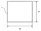
- FIG. 1 It is a perspective view which shows the column-shaped titanium raw material used with the manufacturing method of embodiment. It is a front view of the titanium raw material shown in FIG. It is a top view which shows the processing direction with respect to the titanium raw material shown in FIG.
- a titanium material 1 having a columnar shape is prepared as a titanium material.
- the titanium material 1 is made of a titanium ingot or a titanium billet.
- the cylindrical titanium material 1 has a diameter W and a thickness H.
- the size of the titanium material 1 is not particularly limited, but the thickness H is preferably in the range of 20 to 200 mm, and the diameter W is preferably in the range of 100 to 300 mm.
- the titanium material 1 having such a size is easy to handle.
- the titanium material 1 is preferably an ingot or billet produced by a casting method using an electron beam (EB) melting method or the like.
- the purity (titanium purity) of the titanium material 1 is preferably 99.99% or more (4N or more). Since the purity of the sputtering target (titanium target) conforms to the purity of the titanium material 1, when producing a sputtering target having a purity of 99.99% or more, use the titanium material 1 having a purity of 99.99% or more. Is preferred. When producing a sputtering target having a purity of 99.999% or more (5N or more), it is preferable to use a titanium material 1 having a purity of 99.999% or more.
- two sets of cold forging are performed on a columnar titanium material 1 with one set of cold forging in a direction perpendicular to the direction parallel to the thickness direction.
- the 1st kneading forging process given above is performed.
- the direction parallel to the thickness direction of the titanium material 1 is the thickness H direction in FIG. 2, and the direction perpendicular to the thickness direction is the diameter W direction in FIG.
- kneading forging including cold forging in the thickness H direction and cold forging in the diameter W direction is set as one set, two or more sets are performed.
- the crystal grain size of the titanium material 1 can be refined and the crystal orientation is suppressed from being biased to a specific direction. Furthermore, the remaining of the cast structure of the titanium material 1 manufactured by casting, that is, the generation of so-called ghost grains can be suppressed.
- the Vickers hardness (average value) of the titanium material 1 that has undergone the first kneading forging process is Hv 170 or more.
- the homogeneity of the structure is improved and the hardness of the titanium material 1 is increased.
- the first kneading forging process is performed so that the Vickers hardness of the titanium material 1 is Hv 170 or more.
- the cold forging process in the diameter W direction does not always apply pressure in a fixed direction.
- the first set applies pressure in the direction of arrow X
- the second set indicates arrow Y. It is preferable to change the direction in which the pressure is applied, such as applying pressure in the direction. It is also effective to change the direction in which pressure is applied in one set.
- the effect of refining the crystal grain size of the titanium material 1 and the effect of suppressing the deviation of the crystal orientation can also be enhanced by changing the direction in which the pressure is applied.
- the first kneading forging step is performed by cold forging. When hot forging is performed, surface cracks are likely to occur due to oxidation. Further, since crystal grain growth occurs, a fine crystal structure cannot be obtained.
- a first heat treatment step is performed in which the titanium material 1 that has undergone the first kneading forging step is heated to a temperature of 700 ° C. or higher and recrystallized.
- the first heat treatment step is preferably performed by holding at a temperature in the range of 700 to 1000 ° C. for 0.5 to 10 hours. If the heat treatment temperature exceeds 1000 ° C. or the heat treatment time exceeds 10 hours, grain growth may occur.
- the heat treatment temperature is more preferably in the range of 800 to 900 ° C.
- the heat treatment time is more preferably in the range of 1 to 5 hours.
- the atmosphere during the heat treatment is preferably a vacuum atmosphere of 0.133 Pa or less. In an oxygen-containing atmosphere, the surface of the titanium material 1 may be oxidized during the heat treatment.
- a second kneading forging step is performed in which the titanium material 1 that has undergone the first heat treatment step is kneaded. Also in the second kink forging step, two or more sets of kink forging are performed in which the cold forging process in the thickness H direction and the diameter W direction is one set, as in the first kink forging step. In the second kneading and forging step, it is preferable to perform 2 to 4 sets of kneading and forging. In addition, it is preferable to change the pressure direction applied in the diameter W direction between the first set and the second set. The second kneading forging process is also performed by cold forging. By the second kneading forging step, the crystal grain size can be further refined.
- the cold rolling process is a process of plastic processing the titanium material 1 into a plate shape. You may perform a cold rolling process twice or more as needed.
- the plate thickness of the titanium material 1 is preferably 20 mm or less, more preferably 10 to 15 mm, by a cold rolling process.
- the titanium material 1 having a plate thickness prepared in the cold rolling process is cut to obtain a sputtering target having a desired plate thickness. It is better not to perform the heat treatment step between the second kneading forging step and the cold rolling step. It is preferable to cold-roll the titanium material 1 homogenized in the second kneading forging process as it is.
- the processing rate in the first kneading forging step, the second kneading forging step, and the cold rolling step is arbitrary, but is selected from the first kneading forging step, the second kneading forging step, and the cold rolling step. It is preferable to implement at least one step so that the processing rate is 40% or more.
- the processing rate in the first and second kneading forging processes is a reduction rate (cross-sectional reduction rate) of the cross-sectional area in the diameter W direction of the cylindrical titanium material 1 or the thickness H direction of the cylindrical titanium material 1. It is a reduction rate (thickness reduction rate), and both indicate the cross-sectional area or thickness reduction rate (processing rate) per set.
- the processing rate in the cold rolling process is a reduction rate (thickness reduction rate) in the thickness H direction of the cylindrical titanium material 1.
- the process with a processing rate of 40% or more is a cold process.
- a processing rate forging step ⁇ first heat treatment step ⁇ second kneading forging step
- the occurrence of internal strain Can be suppressed.
- the processing rate is low, the occurrence of internal strain can be suppressed, but each process is repeated many times, resulting in an increase in manufacturing time and manufacturing cost. For this reason, it is preferable that a processing rate shall be 40% or more in any process.
- the process with a processing rate of 40% or more may be any one of the first kneading forging process, the second kneading forging process, and the cold rolling process, or any two processes. Alternatively, all steps may be used.
- the upper limit of the processing rate is preferably 80% or less. When the processing rate in one step exceeds 80%, internal distortion, cracks, wrinkles and the like are likely to occur.
- a second heat treatment step is performed in which the titanium material 1 that has undergone the cold rolling step is heated to a temperature of 300 ° C. or higher.
- the second heat treatment step is preferably performed by holding at a temperature in the range of 300 to 600 ° C. for 2 to 5 hours.
- the heat treatment temperature is more preferably in the range of 400 to 600 ° C.
- the atmosphere during the heat treatment is preferably a vacuum atmosphere of 0.133 Pa or less. In an oxygen-containing atmosphere, the surface of the plate-like titanium material may be oxidized during the heat treatment.
- a plate-like titanium material that has undergone the second heat treatment step is machined to produce a sputtering target.
- the machining of the plate-like titanium material is performed by a cutting process such as a lathe process.
- a target sputtering target can be obtained.
- the obtained sputtering target is bonded to the backing plate by diffusion bonding.
- the crystal grain size is refined in the first and second kneading and forging steps, and the deviation in crystal orientation is suppressed, so that the average crystal grain size is 15 ⁇ m or less.
- a sputtering target titanium target
- a sputtering target having a purity of 99.99% or more and having a fine crystal structure and random orientation can be obtained.
- a fine crystal structure having an average crystal grain size of 15 ⁇ m or less can be obtained, and the crystal orientation is random orientation. can do.
- a sputtering target having a Vickers hardness of a sputtering surface of Hv 90 to 110 and a Vickers hardness variation of 3% or less can be obtained. That is, a homogeneous state can be obtained by combining kneading forging and heat treatment.
- a titanium material having a Vickers hardness of Hv 170 or higher by kneading forging can be softened by heat treatment (Hv 90 to 110).
- Hv 90 to 110 By repeating such a process, a sputtering target having a fine and homogeneous structure can be obtained.
- the average crystal grain size is measured by the line intercept method.
- the line intercept method is implemented as follows. First, an enlarged photograph of the measurement target part is taken with an optical micrograph. The magnified photograph is a photograph in which a unit area of 500 ⁇ m ⁇ 500 ⁇ m is magnified. An arbitrary straight line (length of 500 ⁇ m) is drawn on such an enlarged photograph, the number of Ti crystal grains on the line is counted, and the average crystal grain size is obtained by “500 ⁇ m / number of crystal grains on straight line 500 ⁇ m”. . Such an operation is performed three times, and the average value of the measured values is defined as the average crystal grain size.
- the crystal orientation of the sputtering surface is random, and the random orientation is maintained over the entire thickness direction of the sputtering target, so that the change in the sputtering rate during sputtering can be suppressed. . Accordingly, uniform film formation can be performed.
- a titanium nitride (TiN) film is formed by sputtering in a nitrogen atmosphere using the sputtering target of this embodiment, for example, the densest surface can be grown in a columnar shape.
- a titanium nitride film is suitable for a barrier film of a wiring layer (Al wiring or the like) of a semiconductor element.
- Random crystal orientation can be measured by X-ray diffraction (XRD).
- XRD X-ray diffraction
- the randomly oriented titanium target has a relative intensity I (100) of the diffraction peak from the (100) plane of titanium and the diffraction peak from the (002) plane of titanium.
- the relative intensity I (002) and the relative intensity I (101) of the diffraction peak from the (101) plane of titanium decrease in the order of I (101) > I (002) > I (100) .
- the titanium target is in a random orientation.
- the crystal is oriented in a specific orientation, the order of the relative intensity ratios of the crystal planes is shifted.
- the order of the relative intensity ratio of each crystal plane is the same. That is, when X-ray diffraction in the depth direction is measured, the relative intensity I (100) of the diffraction peak from the (100) plane of titanium and the relative intensity I (002) of the diffraction peak from the (002) plane of titanium The relative intensity I (101) of the diffraction peak from the (101) plane of titanium decreases in the order of I (101) > I (002) > I (100) .
- peaks of crystal planes other than the (100) plane, (002) plane, and (101) plane are also detected.
- the (100) plane, (002) It is important to compare the relative intensities of the peaks on the) plane and the (101) plane. The reason is that these crystal plane peaks are the three main peaks from the highest intensity of PDF data.
- the measurement conditions of the X-ray diffraction method are a Cu target, a tube voltage of 40 kV, a tube current of 40 mA, a scattering slit of 0.63 mm, and a light receiving slit of 0.15 mm.
- the presence or absence of ghost grains in the sputtering target can also be determined by the X-ray diffraction method described above.
- the presence or absence of ghost grains can also be determined from an enlarged photograph taken with an optical microscope. In a magnified photograph (structure photograph) obtained by an optical microscope, when ghost grains are present, a structure in which the grain boundaries of Ti crystal grains are unclear is recognized.
- the random orientation of the sputtering surface is maintained over the thickness direction. For this reason, even if a sputtering target having a thickness of 10 mm or more is sputtered for a long time, the sputtering rate hardly changes and a highly reliable sputtering characteristic is exhibited. Even if the sputtering target has a large sputtering target with a diameter of 300 mm or more, an average crystal grain size of 15 ⁇ m or less and a homogeneous random orientation can be maintained. For this reason, it is possible to obtain a uniform state in which the Vickers hardness of the sputtering surface is Hv 90 to 110 and the variation of the Vickers hardness is 3% or less.
- the method for manufacturing a semiconductor device of this embodiment includes a step of sputtering a thin film containing titanium using the sputtering target of the above-described embodiment.
- the film forming step is a step of forming a titanium nitride film, for example, by sputtering a sputtering target (titanium target) in nitrogen.
- a titanium nitride film formed using the sputtering target of this embodiment is suitable as a barrier film of a semiconductor element. According to the sputtering target of this embodiment, since reliability can be maintained even when used for a long period of time, it is possible to improve the reliability of the semiconductor element.
- Examples 1 to 5, Comparative Example 1 A titanium material having a diameter W of 100 to 300 mm and a thickness H of 100 to 200 mm (high purity titanium billet having a purity of 99.99% by mass or more) was prepared, and a sputtering target manufacturing process whose conditions are shown in Table 1 was performed.
- the processing rate of the kneading forging process of Table 1 shows the larger value among the cross-section reduction rate in the diameter W direction and the thickness reduction rate in the thickness H direction.
- the first and second kneading forging steps were performed so that at least one of the cross-section reduction rate and the thickness reduction rate was the processing rate shown in Table 1.
- the titanium material obtained by the manufacturing process shown in Table 1 was turned to produce a titanium target whose size is shown in Table 2.
- the average crystal grain size of each target was measured, and the presence or absence of random orientation was further confirmed.
- the average crystal grain size was measured by the method described above. The results are shown in Table 2.
- X-ray diffraction was performed on the sputter surface and a portion dug to a depth of 10 mm from the sputter surface, and diffraction from the (100) plane, (002) plane, and (101) plane at each measurement location. The determination was made by measuring the relative intensity of the peaks.
- Table 2 shows the order of the relative intensities of the diffraction peaks from each crystal plane. All of the titanium targets had a recrystallized structure.
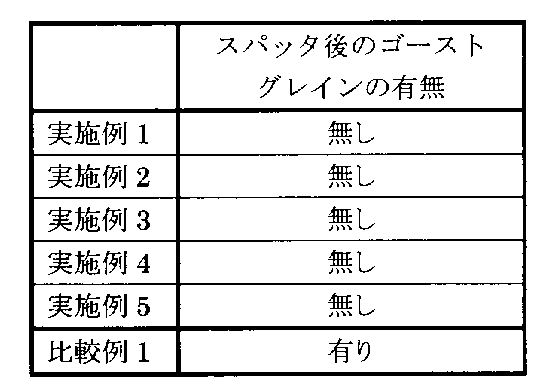
- the titanium targets according to Examples 1 to 5 did not have ghost grains, and showed stable sputtering characteristics until the remaining thickness reached 2 mm.
- the titanium target of the comparative example was 5 mm deep and ghost grain was confirmed. From this result, it can be seen that the titanium target according to the example shows highly reliable sputtering characteristics. Therefore, it is possible to improve the reliability of the semiconductor element by forming the barrier film (TiN film) of the semiconductor element using the titanium target of the embodiment. Furthermore, since the amount of titanium to be reused (most dissolved) can be reduced, the titanium targets of the examples are excellent in terms of material efficiency.
Landscapes
- Chemical & Material Sciences (AREA)
- Chemical Kinetics & Catalysis (AREA)
- Engineering & Computer Science (AREA)
- Materials Engineering (AREA)
- Mechanical Engineering (AREA)
- Metallurgy (AREA)
- Organic Chemistry (AREA)
- Physical Vapour Deposition (AREA)
- Electrodes Of Semiconductors (AREA)
Abstract
Description
直径Wが100~300mm、厚さHが100~200mmのチタン素材(純度99.99質量%以上の高純度チタンビレット)を用意し、表1に条件を示すスパッタリングターゲットの製造工程を実施した。なお、表1のこねくり鍛造工程の加工率は、直径W方向の断面減少率、および厚さH方向の厚さ減少率のうち、大きい方の値を示す。第1および第2のこねくり鍛造工程は、断面減少率および厚さ減少率の少なくとも一方が表1に示す加工率となるように実施した。


Claims (18)
- 円柱形状のチタン素材に、前記チタン素材の厚さ方向に対して平行な方向と垂直な方向の冷間鍛造加工を1セットとするこねくり鍛造を、2セット以上施す第1のこねくり鍛造工程と、
前記第1のこねくり鍛造工程を経たチタン材を、700℃以上の温度に加熱して再結晶化させる第1の熱処理工程と、
前記第1の熱処理工程を経たチタン材を、前記チタン材の厚さ方向に対して平行な方向と垂直な方向の冷間鍛造加工を1セットとするこねくり鍛造を、2セット以上施す第2のこねくり鍛造工程と、
前記第2のこねくり鍛造工程を経たチタン材を、冷間圧延する冷間圧延工程と、
前記冷間圧延工程を経たチタン材を、300℃以上の温度に加熱して熱処理する第2の熱処理工程と、
前記第2の熱処理工程を経たチタン材を機械加工してスパッタリングターゲットを作製する工程と
を具備することを特徴とするスパッタリングターゲットの製造方法。 - 請求項1記載のスパッタリングターゲットの製造方法において、
前記第1のこねくり鍛造工程、前記第2のこねくり鍛造工程、および前記冷間圧延工程から選ばれる少なくとも1つの工程は、加工率が40%以上となるように実施されることを特徴とするスパッタリングターゲットの製造方法。 - 請求項2記載のスパッタリングターゲットの製造方法において、
前記加工率は40%以上80%以下であることを特徴とするスパッタリングターゲットの製造方法。 - 請求項1記載のスパッタリングターゲットの製造方法において、
前記第1のこねくり鍛造工程は、断面減少率および厚さ減少率の少なくとも一方が40%以上となるように実施されることを特徴とするスパッタリングターゲットの製造方法。 - 請求項1記載のスパッタリングターゲットの製造方法において、
前記第2のこねくり鍛造工程は、断面減少率および厚さ減少率の少なくとも一方が40%以上となるように実施されることを特徴とするスパッタリングターゲットの製造方法。 - 請求項1記載のスパッタリングターゲットの製造方法において、
前記冷間圧延工程は、厚さ減少率が40%以上となるように実施されることを特徴とするスパッタリングターゲットの製造方法。 - 請求項1記載のスパッタリングターゲットの製造方法において、
前記第1のこねくり鍛造工程を経たチタン材のビッカース硬さがHv170以上であることを特徴とするスパッタリングターゲットの製造方法。 - 請求項1記載のスパッタリングターゲットの製造方法において、
前記冷間圧延工程を2回以上行うことを特徴とするスパッタリングターゲットの製造方法。 - 請求項1記載のスパッタリングターゲットの製造方法において、
前記スパッタリングターゲットのチタンの純度が99.99質量%以上であることを特徴とするスパッタリングターゲットの製造方法。 - 請求項1記載のスパッタリングターゲットの製造方法において、
前記スパッタリングターゲットの平均結晶粒径が15μm以下であることを特徴とするスパッタリングターゲットの製造方法。 - 請求項1記載のスパッタリングターゲットの製造方法において、
前記スパッタリングターゲットの結晶配向がランダム配向であることを特徴とするスパッタリングターゲットの製造方法。 - 純度が99.99質量%以上で、かつ平均結晶粒径が15μm以下のチタン材からなり、スパッタ面を有するスパッタリングターゲットであって、
前記スパッタ面のX線回折を測定したとき、前記スパッタ面は(100)面からの回折ピークの相対強度I(100)と(002)面からの回折ピークの相対強度I(002)と(101)面からの回折ピークの相対強度I(101)とがI(101)>I(002)>I(100)の条件を満足することを特徴とするスパッタリングターゲット。 - 請求項12記載のスパッタリングターゲットにおいて、
前記スパッタ面の結晶配向がランダム配向であることを特徴とするスパッタリングターゲット。 - 請求項12記載のスパッタリングターゲットにおいて、
厚さが10mm以上であることを特徴とするスパッタリングターゲット。 - 請求項12記載のスパッタリングターゲットにおいて、
直径が300mm以上であることを特徴とするスパッタリングターゲット。 - 請求項12記載のスパッタリングターゲットにおいて、
前記スパッタリングターゲットの深さ方向に前記スパッタ面と平行な部分のX線回折を測定したとき、(100)面からの回折ピークの相対強度I(100)と(002)面からの回折ピークの相対強度I(002)と(101)面からの回折ピークの相対強度I(101)とがI(100)<I(002)<I(101)の条件を満足することを特徴とするスパッタリングターゲット。 - 請求項12記載のスパッタリングターゲットを用いて、チタンを含む薄膜をスパッタ成膜する工程を具備することを特徴とする半導体素子の製造方法。
- 請求項17記載の半導体素子の製造方法において、
前記薄膜は金属配線層のバリア膜として用いられる窒化チタン膜であることを特徴とする半導体素子の製造方法。
Priority Applications (4)
| Application Number | Priority Date | Filing Date | Title |
|---|---|---|---|
| JP2012504327A JP5718896B2 (ja) | 2010-03-11 | 2011-03-08 | スパッタリングターゲットとその製造方法、および半導体素子の製造方法 |
| CN201180012919.7A CN102791905B (zh) | 2010-03-11 | 2011-03-08 | 溅射靶及其制造方法、以及半导体元件的制造方法 |
| US13/608,406 US9382613B2 (en) | 2010-03-11 | 2012-09-10 | Sputtering target, manufacturing method thereof, and manufacturing method of semiconductor element |
| US16/025,680 USRE47788E1 (en) | 2010-03-11 | 2018-07-02 | Sputtering target, manufacturing method thereof, and manufacturing method of semiconductor element |
Applications Claiming Priority (2)
| Application Number | Priority Date | Filing Date | Title |
|---|---|---|---|
| JP2010-055100 | 2010-03-11 | ||
| JP2010055100 | 2010-03-11 |
Related Child Applications (1)
| Application Number | Title | Priority Date | Filing Date |
|---|---|---|---|
| US13/608,406 Continuation US9382613B2 (en) | 2010-03-11 | 2012-09-10 | Sputtering target, manufacturing method thereof, and manufacturing method of semiconductor element |
Publications (1)
| Publication Number | Publication Date |
|---|---|
| WO2011111373A1 true WO2011111373A1 (ja) | 2011-09-15 |
Family
ID=44563206
Family Applications (1)
| Application Number | Title | Priority Date | Filing Date |
|---|---|---|---|
| PCT/JP2011/001345 Ceased WO2011111373A1 (ja) | 2010-03-11 | 2011-03-08 | スパッタリングターゲットとその製造方法、および半導体素子の製造方法 |
Country Status (4)
| Country | Link |
|---|---|
| US (2) | US9382613B2 (ja) |
| JP (1) | JP5718896B2 (ja) |
| CN (1) | CN102791905B (ja) |
| WO (1) | WO2011111373A1 (ja) |
Cited By (6)
| Publication number | Priority date | Publication date | Assignee | Title |
|---|---|---|---|---|
| WO2012144407A1 (ja) * | 2011-04-18 | 2012-10-26 | 株式会社東芝 | 高純度Niスパッタリングターゲットおよびその製造方法 |
| WO2015064087A1 (ja) * | 2013-10-29 | 2015-05-07 | 株式会社 東芝 | スパッタリングターゲットおよびその製造方法、ならびに半導体素子の製造方法 |
| JP2016145384A (ja) * | 2015-02-06 | 2016-08-12 | 株式会社東芝 | スパッタリングターゲットの製造方法、およびスパッタリングターゲット |
| JP2019163544A (ja) * | 2019-04-26 | 2019-09-26 | 株式会社東芝 | スパッタリングターゲット、窒化チタン膜、配線層、および半導体素子 |
| WO2020066956A1 (ja) * | 2018-09-26 | 2020-04-02 | Jx金属株式会社 | スパッタリングターゲット及びその製造方法 |
| CN115341161A (zh) * | 2022-08-22 | 2022-11-15 | 宁波江丰电子材料股份有限公司 | 一种铜铝合金靶材及其制备方法与应用 |
Families Citing this family (7)
| Publication number | Priority date | Publication date | Assignee | Title |
|---|---|---|---|---|
| KR20130076863A (ko) | 2010-10-25 | 2013-07-08 | 제이엑스 닛코 닛세키 킨조쿠 가부시키가이샤 | 스퍼터링용 티탄 타깃 |
| CN104694888B (zh) * | 2013-12-09 | 2017-05-10 | 有研亿金新材料股份有限公司 | 一种高纯铜靶材的制备方法 |
| CN105154834A (zh) * | 2015-09-07 | 2015-12-16 | 云南钛业股份有限公司 | 一种圆柱形钛溅射靶材的生产方法 |
| JP7179450B2 (ja) * | 2017-09-21 | 2022-11-29 | Jx金属株式会社 | スパッタリング用チタンターゲット及びその製造方法、並びにチタン含有薄膜の製造方法 |
| US10760156B2 (en) | 2017-10-13 | 2020-09-01 | Honeywell International Inc. | Copper manganese sputtering target |
| US11035036B2 (en) * | 2018-02-01 | 2021-06-15 | Honeywell International Inc. | Method of forming copper alloy sputtering targets with refined shape and microstructure |
| CN114717528B (zh) * | 2022-04-06 | 2023-09-08 | 宁波江丰电子材料股份有限公司 | 一种含钛靶材及其制备方法 |
Citations (7)
| Publication number | Priority date | Publication date | Assignee | Title |
|---|---|---|---|---|
| JPH08333676A (ja) * | 1995-06-07 | 1996-12-17 | Vacuum Metallurgical Co Ltd | スパッタリング用高純度チタンターゲット及びその製造方法 |
| JPH09143704A (ja) * | 1995-11-27 | 1997-06-03 | Hitachi Metals Ltd | スパッタリング用チタンターゲットおよびその製造方法 |
| JPH10245670A (ja) * | 1998-02-06 | 1998-09-14 | Japan Energy Corp | 高純度チタニウムスパッタリングターゲット |
| JP2000234167A (ja) * | 1999-02-10 | 2000-08-29 | Tokyo Tungsten Co Ltd | Moスパッターリングターゲット材及びその製造方法 |
| JP2002220659A (ja) * | 2000-12-05 | 2002-08-09 | Praxair St Technol Inc | 銅スパッターターゲットの加工及び結合 |
| JP2003253411A (ja) * | 2002-02-27 | 2003-09-10 | Toho Titanium Co Ltd | ターゲット用チタン材の製造方法 |
| WO2005045090A1 (ja) * | 2003-11-06 | 2005-05-19 | Nikko Materials Co., Ltd. | タンタルスパッタリングターゲット |
Family Cites Families (18)
| Publication number | Priority date | Publication date | Assignee | Title |
|---|---|---|---|---|
| US3470034A (en) * | 1967-02-14 | 1969-09-30 | Reactive Metals Inc | Method of refining the macrostructure of titanium alloys |
| US6400025B1 (en) | 1989-07-14 | 2002-06-04 | Kabushiki Kaisha Toshiba | Highly purified titanium material, method for preparation of it and sputtering target using it |
| US5204057A (en) | 1989-07-14 | 1993-04-20 | Kabushiki Kaisha Toshiba | Highly purified titanium material and its named article, a sputtering target |
| JP2918856B2 (ja) | 1989-07-14 | 1999-07-12 | 株式会社東芝 | スパッタターゲットとその製造方法、およびそれを用いて成膜した高純度チタン膜 |
| JP2984778B2 (ja) * | 1995-02-27 | 1999-11-29 | 株式会社住友シチックス尼崎 | 高純度チタン材の鍛造方法 |
| JP2984783B2 (ja) * | 1995-03-13 | 1999-11-29 | 株式会社住友シチックス尼崎 | スパッタリング用チタンターゲットおよびその製造方法 |
| JP3413782B2 (ja) * | 1995-03-31 | 2003-06-09 | 日立金属株式会社 | スパッタリング用チタンタ−ゲットおよびその製造方法 |
| US6045634A (en) * | 1997-08-14 | 2000-04-04 | Praxair S. T. Technology, Inc. | High purity titanium sputtering target and method of making |
| JPH11269621A (ja) * | 1997-12-24 | 1999-10-05 | Toho Titanium Co Ltd | 高純度チタン材の加工方法 |
| US6478902B2 (en) | 1999-07-08 | 2002-11-12 | Praxair S.T. Technology, Inc. | Fabrication and bonding of copper sputter targets |
| US6878250B1 (en) | 1999-12-16 | 2005-04-12 | Honeywell International Inc. | Sputtering targets formed from cast materials |
| US20040072009A1 (en) | 1999-12-16 | 2004-04-15 | Segal Vladimir M. | Copper sputtering targets and methods of forming copper sputtering targets |
| WO2003046250A1 (fr) * | 2001-11-26 | 2003-06-05 | Nikko Materials Company, Limited | Cible de pulverisation et procede de fabrication associe |
| JP4672967B2 (ja) * | 2003-01-10 | 2011-04-20 | Jx日鉱日石金属株式会社 | ターゲットの製造方法 |
| JP4384453B2 (ja) | 2003-07-16 | 2009-12-16 | 株式会社神戸製鋼所 | Ag系スパッタリングターゲット及びその製造方法 |
| US8252126B2 (en) * | 2004-05-06 | 2012-08-28 | Global Advanced Metals, Usa, Inc. | Sputter targets and methods of forming same by rotary axial forging |
| JP4974362B2 (ja) * | 2006-04-13 | 2012-07-11 | 株式会社アルバック | Taスパッタリングターゲットおよびその製造方法 |
| CN100567560C (zh) * | 2007-11-02 | 2009-12-09 | 北京有色金属研究总院 | 嵌套式溅射靶及其制造方法 |
-
2011
- 2011-03-08 CN CN201180012919.7A patent/CN102791905B/zh active Active
- 2011-03-08 JP JP2012504327A patent/JP5718896B2/ja active Active
- 2011-03-08 WO PCT/JP2011/001345 patent/WO2011111373A1/ja not_active Ceased
-
2012
- 2012-09-10 US US13/608,406 patent/US9382613B2/en not_active Ceased
-
2018
- 2018-07-02 US US16/025,680 patent/USRE47788E1/en active Active
Patent Citations (7)
| Publication number | Priority date | Publication date | Assignee | Title |
|---|---|---|---|---|
| JPH08333676A (ja) * | 1995-06-07 | 1996-12-17 | Vacuum Metallurgical Co Ltd | スパッタリング用高純度チタンターゲット及びその製造方法 |
| JPH09143704A (ja) * | 1995-11-27 | 1997-06-03 | Hitachi Metals Ltd | スパッタリング用チタンターゲットおよびその製造方法 |
| JPH10245670A (ja) * | 1998-02-06 | 1998-09-14 | Japan Energy Corp | 高純度チタニウムスパッタリングターゲット |
| JP2000234167A (ja) * | 1999-02-10 | 2000-08-29 | Tokyo Tungsten Co Ltd | Moスパッターリングターゲット材及びその製造方法 |
| JP2002220659A (ja) * | 2000-12-05 | 2002-08-09 | Praxair St Technol Inc | 銅スパッターターゲットの加工及び結合 |
| JP2003253411A (ja) * | 2002-02-27 | 2003-09-10 | Toho Titanium Co Ltd | ターゲット用チタン材の製造方法 |
| WO2005045090A1 (ja) * | 2003-11-06 | 2005-05-19 | Nikko Materials Co., Ltd. | タンタルスパッタリングターゲット |
Cited By (11)
| Publication number | Priority date | Publication date | Assignee | Title |
|---|---|---|---|---|
| WO2012144407A1 (ja) * | 2011-04-18 | 2012-10-26 | 株式会社東芝 | 高純度Niスパッタリングターゲットおよびその製造方法 |
| WO2015064087A1 (ja) * | 2013-10-29 | 2015-05-07 | 株式会社 東芝 | スパッタリングターゲットおよびその製造方法、ならびに半導体素子の製造方法 |
| JPWO2015064087A1 (ja) * | 2013-10-29 | 2017-03-09 | 株式会社東芝 | スパッタリングターゲットおよびその製造方法、ならびに半導体素子の製造方法 |
| JP2020007640A (ja) * | 2013-10-29 | 2020-01-16 | 株式会社東芝 | スパッタリングターゲットおよび半導体素子の製造方法 |
| JP2016145384A (ja) * | 2015-02-06 | 2016-08-12 | 株式会社東芝 | スパッタリングターゲットの製造方法、およびスパッタリングターゲット |
| WO2020066956A1 (ja) * | 2018-09-26 | 2020-04-02 | Jx金属株式会社 | スパッタリングターゲット及びその製造方法 |
| JPWO2020066956A1 (ja) * | 2018-09-26 | 2021-09-24 | Jx金属株式会社 | スパッタリングターゲット及びその製造方法 |
| JP7455750B2 (ja) | 2018-09-26 | 2024-03-26 | Jx金属株式会社 | 円筒形スパッタリングターゲット及びその製造方法 |
| JP2019163544A (ja) * | 2019-04-26 | 2019-09-26 | 株式会社東芝 | スパッタリングターゲット、窒化チタン膜、配線層、および半導体素子 |
| CN115341161A (zh) * | 2022-08-22 | 2022-11-15 | 宁波江丰电子材料股份有限公司 | 一种铜铝合金靶材及其制备方法与应用 |
| CN115341161B (zh) * | 2022-08-22 | 2023-06-23 | 宁波江丰电子材料股份有限公司 | 一种铜铝合金靶材及其制备方法与应用 |
Also Published As
| Publication number | Publication date |
|---|---|
| US9382613B2 (en) | 2016-07-05 |
| JP5718896B2 (ja) | 2015-05-13 |
| CN102791905A (zh) | 2012-11-21 |
| USRE47788E1 (en) | 2019-12-31 |
| US20130001069A1 (en) | 2013-01-03 |
| JPWO2011111373A1 (ja) | 2013-06-27 |
| CN102791905B (zh) | 2015-04-01 |
Similar Documents
| Publication | Publication Date | Title |
|---|---|---|
| JP5718896B2 (ja) | スパッタリングターゲットとその製造方法、および半導体素子の製造方法 | |
| JP5714506B2 (ja) | タンタルスパッタリングターゲットおよびタンタルスパッタリングターゲットの製造方法ならびに半導体素子の製造方法 | |
| JP6721769B2 (ja) | スパッタリングターゲットおよび半導体素子の製造方法 | |
| TWI623638B (zh) | Sputtering target and manufacturing method thereof | |
| WO2013141231A1 (ja) | タンタルスパッタリングターゲット及びその製造方法並びに同ターゲットを用いて形成した半導体配線用バリア膜 | |
| TWI695894B (zh) | 濺鍍用鈦靶及其製造方法、以及含鈦薄膜的製造方法 | |
| WO2012144407A1 (ja) | 高純度Niスパッタリングターゲットおよびその製造方法 | |
| WO2012057057A1 (ja) | スパッタリング用チタンターゲット | |
| JP2017150015A (ja) | スパッタリングターゲット、およびスパッタリングターゲットの製造方法 | |
| TWI707046B (zh) | 鉭濺鍍靶及其製造方法 | |
| TWI676691B (zh) | 鉭濺鍍靶及其製造方法 | |
| JP6377021B2 (ja) | Al合金スパッタリングターゲット | |
| TWI665325B (zh) | Tantalum sputtering target | |
| JP2019163544A (ja) | スパッタリングターゲット、窒化チタン膜、配線層、および半導体素子 | |
| JP2016145384A (ja) | スパッタリングターゲットの製造方法、およびスパッタリングターゲット |
Legal Events
| Date | Code | Title | Description |
|---|---|---|---|
| WWE | Wipo information: entry into national phase |
Ref document number: 201180012919.7 Country of ref document: CN |
|
| 121 | Ep: the epo has been informed by wipo that ep was designated in this application |
Ref document number: 11753038 Country of ref document: EP Kind code of ref document: A1 |
|
| WWE | Wipo information: entry into national phase |
Ref document number: 2012504327 Country of ref document: JP |
|
| NENP | Non-entry into the national phase |
Ref country code: DE |
|
| 122 | Ep: pct application non-entry in european phase |
Ref document number: 11753038 Country of ref document: EP Kind code of ref document: A1 |