WO2011108394A1 - 光学フィルム及びその製造方法 - Google Patents
光学フィルム及びその製造方法 Download PDFInfo
- Publication number
- WO2011108394A1 WO2011108394A1 PCT/JP2011/053773 JP2011053773W WO2011108394A1 WO 2011108394 A1 WO2011108394 A1 WO 2011108394A1 JP 2011053773 W JP2011053773 W JP 2011053773W WO 2011108394 A1 WO2011108394 A1 WO 2011108394A1
- Authority
- WO
- WIPO (PCT)
- Prior art keywords
- optical film
- hard coat
- coat layer
- fine particles
- resin
- Prior art date
- Legal status (The legal status is an assumption and is not a legal conclusion. Google has not performed a legal analysis and makes no representation as to the accuracy of the status listed.)
- Ceased
Links
Images

Classifications
-
- G—PHYSICS
- G02—OPTICS
- G02B—OPTICAL ELEMENTS, SYSTEMS OR APPARATUS
- G02B1/00—Optical elements characterised by the material of which they are made; Optical coatings for optical elements
- G02B1/10—Optical coatings produced by application to, or surface treatment of, optical elements
-
- G02B1/105—
-
- B—PERFORMING OPERATIONS; TRANSPORTING
- B32—LAYERED PRODUCTS
- B32B—LAYERED PRODUCTS, i.e. PRODUCTS BUILT-UP OF STRATA OF FLAT OR NON-FLAT, e.g. CELLULAR OR HONEYCOMB, FORM
- B32B27/00—Layered products comprising a layer of synthetic resin
- B32B27/18—Layered products comprising a layer of synthetic resin characterised by the use of special additives
-
- B—PERFORMING OPERATIONS; TRANSPORTING
- B32—LAYERED PRODUCTS
- B32B—LAYERED PRODUCTS, i.e. PRODUCTS BUILT-UP OF STRATA OF FLAT OR NON-FLAT, e.g. CELLULAR OR HONEYCOMB, FORM
- B32B27/00—Layered products comprising a layer of synthetic resin
- B32B27/18—Layered products comprising a layer of synthetic resin characterised by the use of special additives
- B32B27/26—Layered products comprising a layer of synthetic resin characterised by the use of special additives using curing agents
-
- B—PERFORMING OPERATIONS; TRANSPORTING
- B32—LAYERED PRODUCTS
- B32B—LAYERED PRODUCTS, i.e. PRODUCTS BUILT-UP OF STRATA OF FLAT OR NON-FLAT, e.g. CELLULAR OR HONEYCOMB, FORM
- B32B5/00—Layered products characterised by the non- homogeneity or physical structure, i.e. comprising a fibrous, filamentary, particulate or foam layer; Layered products characterised by having a layer differing constitutionally or physically in different parts
- B32B5/16—Layered products characterised by the non- homogeneity or physical structure, i.e. comprising a fibrous, filamentary, particulate or foam layer; Layered products characterised by having a layer differing constitutionally or physically in different parts characterised by features of a layer formed of particles, e.g. chips, powder or granules
-
- B—PERFORMING OPERATIONS; TRANSPORTING
- B32—LAYERED PRODUCTS
- B32B—LAYERED PRODUCTS, i.e. PRODUCTS BUILT-UP OF STRATA OF FLAT OR NON-FLAT, e.g. CELLULAR OR HONEYCOMB, FORM
- B32B7/00—Layered products characterised by the relation between layers; Layered products characterised by the relative orientation of features between layers, or by the relative values of a measurable parameter between layers, i.e. products comprising layers having different physical, chemical or physicochemical properties; Layered products characterised by the interconnection of layers
- B32B7/02—Physical, chemical or physicochemical properties
-
- C—CHEMISTRY; METALLURGY
- C08—ORGANIC MACROMOLECULAR COMPOUNDS; THEIR PREPARATION OR CHEMICAL WORKING-UP; COMPOSITIONS BASED THEREON
- C08F—MACROMOLECULAR COMPOUNDS OBTAINED BY REACTIONS ONLY INVOLVING CARBON-TO-CARBON UNSATURATED BONDS
- C08F2/00—Processes of polymerisation
- C08F2/46—Polymerisation initiated by wave energy or particle radiation
- C08F2/48—Polymerisation initiated by wave energy or particle radiation by ultraviolet or visible light
-
- G—PHYSICS
- G02—OPTICS
- G02B—OPTICAL ELEMENTS, SYSTEMS OR APPARATUS
- G02B1/00—Optical elements characterised by the material of which they are made; Optical coatings for optical elements
-
- G—PHYSICS
- G02—OPTICS
- G02B—OPTICAL ELEMENTS, SYSTEMS OR APPARATUS
- G02B1/00—Optical elements characterised by the material of which they are made; Optical coatings for optical elements
- G02B1/10—Optical coatings produced by application to, or surface treatment of, optical elements
- G02B1/14—Protective coatings, e.g. hard coatings
-
- G—PHYSICS
- G02—OPTICS
- G02B—OPTICAL ELEMENTS, SYSTEMS OR APPARATUS
- G02B1/00—Optical elements characterised by the material of which they are made; Optical coatings for optical elements
- G02B1/10—Optical coatings produced by application to, or surface treatment of, optical elements
- G02B1/16—Optical coatings produced by application to, or surface treatment of, optical elements having an anti-static effect, e.g. electrically conducting coatings
-
- G—PHYSICS
- G02—OPTICS
- G02F—OPTICAL DEVICES OR ARRANGEMENTS FOR THE CONTROL OF LIGHT BY MODIFICATION OF THE OPTICAL PROPERTIES OF THE MEDIA OF THE ELEMENTS INVOLVED THEREIN; NON-LINEAR OPTICS; FREQUENCY-CHANGING OF LIGHT; OPTICAL LOGIC ELEMENTS; OPTICAL ANALOGUE/DIGITAL CONVERTERS
- G02F1/00—Devices or arrangements for the control of the intensity, colour, phase, polarisation or direction of light arriving from an independent light source, e.g. switching, gating or modulating; Non-linear optics
- G02F1/01—Devices or arrangements for the control of the intensity, colour, phase, polarisation or direction of light arriving from an independent light source, e.g. switching, gating or modulating; Non-linear optics for the control of the intensity, phase, polarisation or colour
- G02F1/13—Devices or arrangements for the control of the intensity, colour, phase, polarisation or direction of light arriving from an independent light source, e.g. switching, gating or modulating; Non-linear optics for the control of the intensity, phase, polarisation or colour based on liquid crystals, e.g. single liquid crystal display cells
- G02F1/133—Constructional arrangements; Operation of liquid crystal cells; Circuit arrangements
- G02F1/1333—Constructional arrangements; Manufacturing methods
- G02F1/1335—Structural association of cells with optical devices, e.g. polarisers or reflectors
-
- G—PHYSICS
- G02—OPTICS
- G02F—OPTICAL DEVICES OR ARRANGEMENTS FOR THE CONTROL OF LIGHT BY MODIFICATION OF THE OPTICAL PROPERTIES OF THE MEDIA OF THE ELEMENTS INVOLVED THEREIN; NON-LINEAR OPTICS; FREQUENCY-CHANGING OF LIGHT; OPTICAL LOGIC ELEMENTS; OPTICAL ANALOGUE/DIGITAL CONVERTERS
- G02F1/00—Devices or arrangements for the control of the intensity, colour, phase, polarisation or direction of light arriving from an independent light source, e.g. switching, gating or modulating; Non-linear optics
- G02F1/01—Devices or arrangements for the control of the intensity, colour, phase, polarisation or direction of light arriving from an independent light source, e.g. switching, gating or modulating; Non-linear optics for the control of the intensity, phase, polarisation or colour
- G02F1/13—Devices or arrangements for the control of the intensity, colour, phase, polarisation or direction of light arriving from an independent light source, e.g. switching, gating or modulating; Non-linear optics for the control of the intensity, phase, polarisation or colour based on liquid crystals, e.g. single liquid crystal display cells
- G02F1/133—Constructional arrangements; Operation of liquid crystal cells; Circuit arrangements
- G02F1/1333—Constructional arrangements; Manufacturing methods
- G02F1/1335—Structural association of cells with optical devices, e.g. polarisers or reflectors
- G02F1/133502—Antiglare, refractive index matching layers
-
- Y—GENERAL TAGGING OF NEW TECHNOLOGICAL DEVELOPMENTS; GENERAL TAGGING OF CROSS-SECTIONAL TECHNOLOGIES SPANNING OVER SEVERAL SECTIONS OF THE IPC; TECHNICAL SUBJECTS COVERED BY FORMER USPC CROSS-REFERENCE ART COLLECTIONS [XRACs] AND DIGESTS
- Y10—TECHNICAL SUBJECTS COVERED BY FORMER USPC
- Y10T—TECHNICAL SUBJECTS COVERED BY FORMER US CLASSIFICATION
- Y10T428/00—Stock material or miscellaneous articles
- Y10T428/24—Structurally defined web or sheet [e.g., overall dimension, etc.]
- Y10T428/24355—Continuous and nonuniform or irregular surface on layer or component [e.g., roofing, etc.]
- Y10T428/24372—Particulate matter
- Y10T428/24413—Metal or metal compound
-
- Y—GENERAL TAGGING OF NEW TECHNOLOGICAL DEVELOPMENTS; GENERAL TAGGING OF CROSS-SECTIONAL TECHNOLOGIES SPANNING OVER SEVERAL SECTIONS OF THE IPC; TECHNICAL SUBJECTS COVERED BY FORMER USPC CROSS-REFERENCE ART COLLECTIONS [XRACs] AND DIGESTS
- Y10—TECHNICAL SUBJECTS COVERED BY FORMER USPC
- Y10T—TECHNICAL SUBJECTS COVERED BY FORMER US CLASSIFICATION
- Y10T428/00—Stock material or miscellaneous articles
- Y10T428/25—Web or sheet containing structurally defined element or component and including a second component containing structurally defined particles
-
- Y—GENERAL TAGGING OF NEW TECHNOLOGICAL DEVELOPMENTS; GENERAL TAGGING OF CROSS-SECTIONAL TECHNOLOGIES SPANNING OVER SEVERAL SECTIONS OF THE IPC; TECHNICAL SUBJECTS COVERED BY FORMER USPC CROSS-REFERENCE ART COLLECTIONS [XRACs] AND DIGESTS
- Y10—TECHNICAL SUBJECTS COVERED BY FORMER USPC
- Y10T—TECHNICAL SUBJECTS COVERED BY FORMER US CLASSIFICATION
- Y10T428/00—Stock material or miscellaneous articles
- Y10T428/25—Web or sheet containing structurally defined element or component and including a second component containing structurally defined particles
- Y10T428/256—Heavy metal or aluminum or compound thereof
Definitions
- the present invention relates to an optical film used for a display device in a display unit of electrical or electronic equipment or precision equipment, and a method for manufacturing the same.
- liquid crystal displays have made remarkable progress as display devices for television (TV) applications or video display applications, and are rapidly spreading.
- the development of high-speed liquid crystal materials and the improvement of driving methods such as overdrive have overcome the conventional video display that LCDs were not good at, and production technology innovations that responded to larger displays Yes.
- the surface is usually treated to prevent reflection of external light. It is.
- One of the techniques is anti-glare treatment, and for example, the surface of a liquid crystal display is usually subjected to anti-glare treatment.
- the anti-glare treatment is a treatment that creates a fine uneven structure on the surface, thereby scattering the reflected light on the surface and blurring the reflected image.
- an anti-glare treatment is applied to an LCD.
- a dazzling film is provided.
- touch panel coordinate input device
- a lightweight and thin display such as a liquid crystal display can be made keyboard-less, and its features are alive. Therefore, touch panels are increasingly used in mobile devices.
- the touch panel can be classified into an optical method, an ultrasonic method, a capacitance method, a resistance film method, and the like according to a position detection method.
- the resistive film method has rapidly spread in recent years because of its simple structure and excellent price / performance ratio.
- a resistive film type touch panel is an electrical component configured by holding two films or sheets at regular intervals with transparent electrodes facing each other.
- the operation method of the touch panel is to fix the one transparent electrode, press the other transparent electrode with a pen or finger from the viewing side, bend it, and contact and conduct with the fixed transparent electrode. The position is detected and a predetermined input is made.
- a touch panel operation method when an electrode is pressed with a pen or a finger, a rainbow pattern due to interference (a so-called “Newton ring” interference color) is formed around the finger or the pointing jig such as the pen. (Or interference fringes) may appear, reducing the visibility of the screen.
- the LCD and the touch panel are provided with an optical film (or light scattering film) having a concavo-convex structure on the surface
- this optical film is usually composed of fine particles such as resin fine particles and silica fine particles, and a binder resin or It is obtained by applying a mixture with a curable resin to a substrate and forming a fine concavo-convex structure on the surface.
- high-definition display devices with a small pixel size have been developed for LCDs and the like, but screen glare and letter blurring are likely to occur, and the size of fine particles to be added and the particle size distribution are narrow. Attempts have been made to control the irregular shape of the surface using sharp fine particles.
- silica fine particles 200 nm silica fine particles, (b) a silica fine particle having a primary particle size of 1 to 30 nm and a binder, and a silica fine particle aggregated structure, the center line average roughness Ra of the hard coat layer side surface of the antiglare film Disclosed is an antiglare film having a roughness period ⁇ a of 40 to 200 ⁇ m and a haze value of 0.1 to 3.0%.
- the content of silica fine particles is described as 0.05 to 30% by weight (particularly 0.2 to 25% by weight) of the film weight.
- 1.5 to 10 parts by weight are blended.
- a flocculant such as alkyl acetoacetate aluminum diisopropylate is described.
- the hard coat layer is formed only of the curable resin, it is not possible to relieve stress from the outside, and cracks are easily generated. Run. In particular, the durability is not sufficient in applications where the keys are repeatedly pressed like the upper transparent electrode of the touch panel. Further, the optical characteristics are not sufficient, the antiglare property is low, glare is not only seen, and the display of the transmitted image is not clear. In addition, in order to agglomerate a large amount of silica fine particles, a flocculant is necessary, which causes bleed out. Further, since the antistatic property of silica fine particles is not sufficient, in the examples, an antistatic layer containing ITO fine particles is formed separately from the hard coat layer.
- an object of the present invention is to provide an optical film having excellent antiglare property or anti-Newton ring property, and excellent in scratch resistance and mechanical properties, and a method for producing the same.
- Another object of the present invention is to provide an optical film having antistatic properties without requiring an antistatic treatment or an antistatic layer and a method for producing the same.
- Still another object of the present invention is to provide an optical film having moderate flexibility and high keystroke durability in a touch panel or the like and a method for producing the same.
- Another object of the present invention is to provide an optical film in which bleeding out such as a flocculant is suppressed and a method for producing the same.
- the present inventors have formed a hard coat layer with a cured resin composition containing a thermoplastic resin and nanometer-sized metal oxide fine particles on at least one surface of a transparent film.
- a hard coat layer with a cured resin composition containing a thermoplastic resin and nanometer-sized metal oxide fine particles on at least one surface of a transparent film.
- the optical film of the present invention is an optical film including a transparent film and a hard coat layer formed on at least one surface of the transparent film, and the hard coat layer is a cured curable resin precursor.
- a thermoplastic resin and metal oxide fine particles having an average primary particle size of 1 to 100 nm.
- the thermoplastic resin may be a thermoplastic resin that is non-reactive with the curable resin precursor (for example, a non-reactive thermoplastic resin such as a cellulose derivative).
- the ratio of the metal oxide fine particles is about 0.5 to 4 parts by weight with respect to 100 parts by weight of the curable resin precursor.
- the metal oxide fine particles may be at least one fine particle selected from the group consisting of antimony-containing tin oxide, antimony oxide, tin oxide, and zinc oxide.
- the curable resin precursor may be a tetrafunctional or higher functional precursor.
- the hard coat layer may have a concavo-convex structure on the surface with an arithmetic average roughness Ra of 0.03 to 0.15 ⁇ m and an average interval between tops of convex portions Sm of 50 to 300 ⁇ m.
- the hard coat layer contains substantially no flocculant.
- the optical film of the present invention may have a haze of about 0.3 to 4%.
- a low refractive index layer may be further formed on the hard coat layer.
- a coating liquid containing a thermoplastic resin, a curable resin precursor, and metal oxide fine particles having an average primary particle size of 1 to 100 nm is applied to at least one surface of a transparent film, and dried. Also included is a method for producing the optical film that is cured by irradiation with active energy rays. In this method, a coating liquid that does not substantially contain a flocculant may be used as the coating liquid.
- metal oxide is used in the sense that it does not contain silicon oxide such as silica.
- the hard coat layer is formed of a cured resin composition containing a thermoplastic resin and nanometer-sized metal oxide fine particles on at least one surface of the transparent film, the metal oxide fine particles are used as the core.
- An uneven structure is formed, and the antiglare property or anti-Newton ring property of the optical film can be improved, and the scratch resistance and mechanical properties can also be improved.
- the metal oxide fine particles are contained, an optical film having antistatic properties can be obtained without requiring an antistatic treatment or an antistatic layer.
- it contains a thermoplastic resin in addition to the cured resin it has appropriate flexibility and can improve the keystroke durability of a touch panel or the like.
- the metal oxide fine particles are more likely to aggregate than silica, it is possible to form a concavo-convex structure that exhibits excellent optical characteristics without blending a flocculant, so that the bleed-out of flocculants and the like is suppressed. A film is obtained.
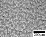
- FIG. 1 is a laser micrograph of the surface of the optical film obtained in Example 1.
- FIG. FIG. 2 is a laser micrograph of the surface of the optical film obtained in Example 4.
- the optical film of the present invention includes a hard coat layer formed on at least one surface (usually one surface) of a transparent film.
- the hard coat layer includes a cured curable resin precursor, a thermoplastic resin, and metal oxide fine particles having an average primary particle size of 1 to 100 nm.
- the curable resin precursor is a compound having a functional group that reacts with heat or active energy rays (such as ultraviolet rays or electron beams), and is cured or crosslinked with heat or active energy rays or the like (particularly cured or crosslinked).
- heat or active energy rays such as ultraviolet rays or electron beams
- Various curable compounds capable of forming (resin) can be used.
- the resin precursor include thermosetting compounds or resins [low molecular weight compounds having an epoxy group, a polymerizable group, an isocyanate group, an alkoxysilyl group, a silanol group, etc.
- photocurable compounds curable with actinic rays such as ultraviolet rays
- photocurable monomers, ultraviolet curable compounds such as oligomers may be an EB (electron beam) curable compound.
- a photocurable compound such as a photocurable monomer, an oligomer, or a photocurable resin that may have a low molecular weight may be simply referred to as a “photocurable resin”.
- the photocurable compound includes, for example, a monomer and an oligomer (or a resin, particularly a low molecular weight resin).
- the monomer can be classified into, for example, a monofunctional monomer having one polymerizable group and a polyfunctional monomer having at least two polymerizable groups.
- Examples of the monofunctional monomer include (meth) acrylic monomers such as (meth) acrylic acid esters, vinyl monomers such as vinylpyrrolidone, isobornyl (meth) acrylate, and adamantyl (meth) acrylate. Examples include (meth) acrylate having a bridged cyclic hydrocarbon group.
- the polyfunctional monomer includes a polyfunctional monomer having about 2 to 8 polymerizable groups.
- the bifunctional monomer include ethylene glycol di (meth) acrylate, propylene glycol di (meth) ) Acrylate, butanediol di (meth) acrylate, neopentyl glycol di (meth) acrylate, alkylene glycol di (meth) acrylate such as hexanediol di (meth) acrylate; diethylene glycol di (meth) acrylate, dipropylene glycol di (meth) ) Acrylates, (poly) oxyalkylene glycol di (meth) acrylates such as polyoxytetramethylene glycol di (meth) acrylate; bridge rings such as tricyclodecane dimethanol di (meth) acrylate and adamantane di (meth) acrylate And di (meth) acrylate having a hydrocarbon group.
- Examples of the tri- to 8-functional monomer include glycerin tri (meth) acrylate, trimethylolpropane tri (meth) acrylate, trimethylolethane tri (meth) acrylate, pentaerythritol tri (meth) acrylate, and pentaerythritol tetra (meth). ) Acrylate, dipentaerythritol penta (meth) acrylate, dipentaerythritol hexa (meth) acrylate, and the like.
- oligomers or resins examples include (meth) acrylates of bisphenol A-alkylene oxide adducts, epoxy (meth) acrylates (bisphenol A type epoxy (meth) acrylates, novolac type epoxy (meth) acrylates, etc.), polyester (meth) acrylates ( For example, aliphatic polyester type (meth) acrylate, aromatic polyester type (meth) acrylate, etc.), (poly) urethane (meth) acrylate (polyester type urethane (meth) acrylate, polyether type urethane (meth) acrylate, etc.), Examples thereof include silicone (meth) acrylate.
- These (meth) acrylate oligomers or resins may contain a copolymerizable monomer exemplified in the section of (meth) acrylic resin in the polymer component.
- These photocurable compounds can be used alone or in combination of two or more.
- the curable resin precursor may contain fluorine atoms or inorganic particles from the viewpoint of improving the strength of the hard coat layer.
- fluorine-containing curable compounds include fluorides of the monomers and oligomers such as fluorinated alkyl (meth) acrylates [for example, perfluorooctylethyl (meth) acrylate and trifluoro Ethyl (meth) acrylate, etc.], fluorinated (poly) oxyalkylene glycol di (meth) acrylate [eg, fluoroethylene glycol di (meth) acrylate, fluoropropylene glycol di (meth) acrylate, etc.], fluorine-containing epoxy resin, urethane Based resins and the like.
- the precursor containing inorganic particles include inorganic particles having a polymerizable group on the surface (for example, silica particles whose surface is modified with a silane coupling agent having a polymerizable group).
- inorganic particles having a polymerizable group on the surface for example, silica particles whose surface is modified with a silane coupling agent having a polymerizable group.
- nanometer-sized silica particles having a polymerizable group on the surface for example, a multifunctional hybrid UV curing agent (Z7501) is commercially available from JSR Corporation.
- a preferable curable resin precursor is a photocurable compound that can be cured in a short time, for example, an ultraviolet curable compound (such as a monomer, an oligomer, or a resin that may have a low molecular weight) or an EB curable compound.
- an ultraviolet curable compound such as a monomer, an oligomer, or a resin that may have a low molecular weight
- an EB curable compound is an ultraviolet curable resin.
- the photocurable resin is a bifunctional or higher (preferably about 2 to 10 functional, more preferably about 3 to 8 functional) photocurable compound, particularly a polyfunctional (meth) acrylate.
- (meth) acrylates for example, esters of 5- to 7-valent polyhydric alcohols such as dipentaerythritol hexa (meth) acrylate and (meth) acrylic acid
- (meth) acrylates for example, esters of 5- to 7-valent polyhydric alcohols such as dipentaerythritol hexa (meth) acrylate and (meth) acrylic acid
- the number average molecular weight of the curable resin precursor is 5000 or less (for example, 300 to 2000), preferably 2000 or less (for example, 500 to 2000), more preferably in consideration of compatibility with the thermoplastic resin described later. It is about 1000 or less (for example, 600 to 1000).
- the curable resin precursor may contain a curing agent depending on the type.
- the thermosetting resin may contain a curing agent such as amines and polyvalent carboxylic acids
- the photocurable resin may contain a photopolymerization initiator.
- the photopolymerization initiator include conventional components such as acetophenones or propiophenones, benzyls, benzoins, benzophenones, thioxanthones, acylphosphine oxides, and the like.
- the content of a curing agent such as a photocuring agent is 0.1 to 20 parts by weight, preferably 0.5 to 10 parts by weight, more preferably 1 to 8 parts by weight (100 parts by weight based on 100 parts by weight of the curable resin precursor). In particular, it is about 1 to 5 parts by weight, and may be about 3 to 8 parts by weight.
- the curable resin precursor may contain a curing accelerator.
- the photocurable resin may contain a photocuring accelerator, for example, a tertiary amine (such as a dialkylaminobenzoic acid ester), a phosphine photopolymerization accelerator, and the like.
- Thermoplastic resin is blended to improve mechanical properties such as flexibility with respect to the hard coat layer, and has a non-reactive resin (reactive group involved in the curing reaction) in the curable resin precursor. Resin).
- thermoplastic resins examples include styrene resins [polystyrene, copolymers of styrene and (meth) acrylic monomers, AS resins, styrene-butadiene copolymers, etc.], (meth) acrylic resins, and the like.
- Poly (meth) acrylate such as polymethyl methacrylate, methyl methacrylate- (meth) acrylic acid copolymer, methyl methacrylate- (meth) acrylic acid ester copolymer, methyl methacrylate-acrylic acid ester -(Meth) acrylic acid copolymer, (meth) acrylic acid ester-styrene copolymer (MS resin, etc.), (meth) acrylic acid-methyl (meth) acrylate-isobornyl (meth) acrylate, etc.], organic Acid vinyl ester resin [ethylene-vinyl acetate copolymer, vinyl acetate-vinyl chloride copolymer, vinyl acetate (Meth) acrylic acid ester copolymer, polyvinyl alcohol, ethylene-vinyl alcohol copolymer, polyvinyl acetal resin, etc.], vinyl ether resins (polyvinyl methyl ether, polyvinyl ethyl ether, polyvinyl
- thermoplastic resins styrene copolymer resins, (meth) acrylic elastomers, olefin elastomers, alicyclic olefin elastomers, polyester elastomers, cellulose derivatives, silicone resins, etc. are widely used, but transparent Cellulose derivatives are preferred because they are excellent in heat resistance and heat resistance and can improve mechanical properties such as flexibility.
- Cellulose derivatives include cellulose esters, cellulose ethers, and cellulose carbamates.
- cellulose esters examples include aliphatic organic acid esters (cellulose acetate such as cellulose diacetate and cellulose triacetate; C 2-6 such as cellulose propionate, cellulose butyrate, cellulose acetate propionate, and cellulose acetate butyrate). Acylate), aromatic organic acid esters (C 7-12 aromatic carboxylic acid esters such as cellulose phthalate and cellulose benzoate), inorganic acid esters (eg, cellulose phosphate, cellulose sulfate, etc.), and the like.
- the cellulose esters may be mixed acid esters such as acetic acid and cellulose nitrate esters.
- cellulose ethers include cyanoethyl cellulose; hydroxy C 2-4 alkyl cellulose such as hydroxyethyl cellulose and hydroxypropyl cellulose; C 1-6 alkyl cellulose such as methyl cellulose and ethyl cellulose; carboxymethyl cellulose or a salt thereof, benzyl cellulose, acetylalkyl A cellulose etc. can be illustrated.
- cellulose carbamates include cellulose phenyl carbamate.
- cellulose derivatives can be used alone or in combination of two or more.
- cellulose esters particularly cellulose C 2-6 acylates such as cellulose diacetate, cellulose triacetate, cellulose propionate, cellulose butyrate, cellulose acetate propionate, and cellulose acetate butyrate are preferable.
- the solubility in a solvent is high, the preparation of the coating liquid is easy, the viscosity of the coating liquid can be easily adjusted by adding a small amount, and the aggregation of fine particles in the coating liquid is suppressed.
- cellulose C 2-4 acylates such as cellulose diacetate, cellulose acetate propionate, and cellulose acetate butyrate (particularly cellulose acetate C 3-4 acylate such as cellulose acetate propionate) are preferable. .
- the ratio of the thermoplastic resin is, for example, 0.1 to 30 parts by weight, preferably 0.1 to 20 parts by weight (for example, 0.3 to 15 parts by weight) with respect to 100 parts by weight of the curable resin precursor. More preferably, it is about 0.6 to 10 parts by weight (particularly 1 to 5 parts by weight).
- the ratio of the thermoplastic resin it is possible to adjust the balance between the hard coat property and the mechanical properties such as shock absorption and cushioning properties.
- Metal oxide fine particles In the present invention, by incorporating metal oxide fine particles into the hard coat layer, the resin component is raised with the metal oxide fine particles as nuclei, or an uneven structure with excellent optical properties can be formed on the surface of the hard coat layer. .
- the metal oxide fine particles are excellent in transparency and scratch resistance, and can improve adhesion with the low refractive index layer when a low refractive index layer is formed. Furthermore, since the metal oxide fine particles are excellent in conductivity, the film is imparted with conductivity, and dust adhesion can be suppressed.
- Examples of the metal oxide constituting the metal oxide fine particles include a Group 4A metal oxide (for example, titanium oxide and zirconium oxide) of the periodic table, a Group 5A metal oxide (for example, vanadium oxide), and a Group 6A metal.
- Oxides such as molybdenum oxide and tungsten oxide
- Group 7A metal oxides such as manganese oxide
- Group 8 metal oxides such as nickel oxide and iron oxide
- Group 1B metal oxides such as copper oxide
- Group 2B metal oxides such as zinc oxide
- Group 3B metal oxides such as aluminum oxide and indium oxide
- Group 4B metal oxides such as tin oxide
- Group 5B metal oxides such as antimony oxide
- metal oxide fine particles can be used alone or in combination of two or more.
- metal oxides containing antimony, tin, zinc for example, antimony trioxide, antimony tetroxide, antimony pentoxide, antimony-containing tin oxide (antimony-doped tin oxide), tin oxide, zinc oxide
- the fine particles composed of at least one selected from the group consisting of antimony-containing tin oxide, antimony oxide, tin oxide and zinc oxide are particularly preferable.
- the metal oxide fine particles may be in the form of a dispersion dispersed in a solvent.
- the solvent include water, alcohols (lower alcohols such as methanol, ethanol, isopropanol, butanol, cyclohexanol, etc.), ketones (acetone, methyl ethyl ketone, methyl isobutyl ketone, cyclohexanone, etc.), esters (methyl acetate, acetic acid, etc.).
- solvents can be used alone or in combination of two or more.
- the concentration of the metal oxide fine particles in the dispersion is, for example, about 0.1 to 50% by weight, preferably about 1 to 40% by weight, and more preferably about 5 to 30% by weight.
- a conventional surface treatment may be performed.
- the shape of the metal oxide fine particles is not particularly limited, and examples thereof include a spherical shape, an ellipsoidal shape, a polygonal shape (polygonal pyramid shape, a rectangular parallelepiped shape, a rectangular parallelepiped shape, etc.), a plate shape, a rod shape, and an indefinite shape. From the viewpoint of forming a rough structure, an isotropic shape such as a substantially spherical shape is preferable.
- the average primary particle size of the metal oxide fine particles can be selected from the range of about 1 to 100 nm, for example, 1 to 60 nm (for example, 1 to 50 nm), preferably 2 to 30 nm, more preferably 3 to 15 nm (particularly 5 to 10 nm). ) If the primary particle size is in the above range, the fine particles are appropriately aggregated in the hard coat layer to form nuclei, or an uneven structure can be formed.
- the ratio of the metal oxide fine particles is, for example, 0.1 to 10 parts by weight, preferably 0.3 to 5 parts by weight, and more preferably 0.5 to 4 parts by weight with respect to 100 parts by weight of the curable resin precursor. (Especially 0.6 to 3 parts by weight).
- the amount may be about 0.5 to 2 parts by weight (particularly 0.6 to 1.5 parts by weight) with respect to 100 parts by weight.
- the ratio of the metal oxide fine particles is, for example, 0.1 to 20 parts by weight, preferably 0.3 to 10 parts by weight, and more preferably 0 to 100 parts by weight of the total amount of the curable resin precursor and the thermoplastic resin. It may be about 5 to 5 parts by weight.
- metal oxide fine particles are excellent in electrical conductivity and are widely used as conductive materials.
- they are colored when blended with transparent resin, they usually form an uneven structure to develop antiglare and anti-Newton ring properties. It is not used as fine particles for the purpose.
- an optically effective uneven structure can be formed in a small proportion with respect to the resin component, optical characteristics such as antiglare property and anti-Newton ring property and conductivity are provided. And both.
- the hard coat layer may contain other fine particles as long as the effect of the metal oxide fine particles is not impaired.
- Other fine particles include organic fine particles and inorganic fine particles.
- the organic fine particles are preferably crosslinked resin fine particles from the viewpoint of scratch resistance and the like.
- the crosslinked resin constituting the fine particles includes a crosslinked thermoplastic resin [for example, a crosslinked olefin resin (for example, crosslinked polyethylene, crosslinked polypropylene, etc.), a crosslinked styrene resin (for example, crosslinked polystyrene, crosslinked polydivinylbenzene, crosslinked polyvinyltoluene, Cross-linked styrene-methyl methacrylate copolymer, etc.), cross-linked acrylic resin (eg, cross-linked polymethyl methacrylate, etc.)], thermosetting resin (melamine resin, urea resin, aminobenzoguanamine resin, silicone resin, epoxy resin, Polyurethane) and the like.
- These organic fine particles can be used alone or in combination of two or more.
- Inorganic compounds constituting the inorganic fine particles include inorganic compounds other than metal oxides, such as simple metals, metal sulfates (calcium sulfate, barium sulfate, etc.), metal silicates (calcium silicate, aluminum silicate, magnesium silicate, aluminosilicate) Magnesium), metal phosphate (calcium phosphate, magnesium phosphate, etc.), metal carbonate (magnesium carbonate, heavy calcium carbonate, light calcium carbonate, etc.), metal hydroxide (aluminum hydroxide, calcium hydroxide, hydroxide) Magnesium, etc.), silicon compounds (silica, white carbon, glass, etc.), natural minerals (zeolite, diatomaceous earth, calcined siliceous earth, alumina, talc, mica, kaolin, sericite, bentonite, montmorillonite, smectite, clay, etc.) Is mentioned.
- metal oxides such as simple metals, metal
- the average primary particle size of the other fine particles is not particularly limited, and can be selected, for example, from a range of about 1 nm to 10 ⁇ m.
- the average primary particle size of the metal oxide fine particles may be in the range.
- the ratio of these fine particles is, for example, 50 parts by weight or less, preferably 30 parts by weight or less (for example, 0.01 to 30 parts by weight), more preferably 10 parts by weight or less (100 parts by weight). For example, it is about 0.1 to 10 parts by weight.
- additives such as stabilizers (antioxidants, ultraviolet absorbers, etc.), surfactants, water-soluble polymers, fillers, crosslinking agents, coupling agents, colorants, flame retardants are included in the hard coat layer.
- stabilizers antioxidants, ultraviolet absorbers, etc.
- surfactants water-soluble polymers, fillers, crosslinking agents, coupling agents, colorants, flame retardants are included in the hard coat layer.
- Lubricants, waxes, preservatives, viscosity modifiers, thickeners, leveling agents, antifoaming agents and the like may be included.
- the hard coat layer contains substantially no flocculant.
- action in this invention is concerned also with the kind of curable resin precursor, a thermoplastic resin, a solvent, a mixture ratio, etc.
- the thickness of the hard coat layer is, for example, about 0.5 to 30 ⁇ m, preferably about 1 to 25 ⁇ m, more preferably about 3 to 20 ⁇ m (particularly about 5 to 15 ⁇ m).
- transparent film or sheet examples of the transparent film or sheet (or substrate film) include resin sheets in addition to glass and ceramics.
- resin which comprises a transparent film resin similar to the said hard-coat layer can be used.
- Preferred transparent films include transparent polymer films such as cellulose derivatives [cellulose triacetate (TAC), cellulose acetate such as cellulose diacetate], polyester resins [polyethylene terephthalate (PET), polybutylene terephthalate (PBT), poly Arylate resins, etc.], polysulfone resins [polysulfone, polyethersulfone, etc.], polyether ketone resins [polyether ketone, polyether ether ketone, etc.], polycarbonate resins (bisphenol A type polycarbonate, etc.), polyolefin resins ( Polyethylene, polypropylene, etc.), cyclic polyolefin resin [TOPAS (registered trademark), ARTON (registered trademark), Zeonet ZEONEX (registered trademark)
- optically isotropic transparent film examples include glass, unstretched or stretched plastic sheet or film, for example, polyester (PET, PBT, etc.), cellulose derivatives, particularly cellulose esters (cellulose diacetate, A sheet or film formed of cellulose acetate such as cellulose triacetate, cellulose acetate propionate, cellulose acetate C 3-4 acylate such as cellulose acetate butyrate, or the like is preferable.
- a cellulose derivative is used as the thermoplastic resin of the hard coat layer, the adhesion between the two can be improved by using a film composed of the cellulose derivative as the transparent film.
- the thickness of the transparent film can be selected from the range of, for example, about 5 to 2000 ⁇ m, preferably 15 to 1000 ⁇ m, and more preferably about 20 to 500 ⁇ m.
- a low refractive index layer may be further formed on the hard coat layer in order to reduce the surface reflectance.
- the low refractive index layer a conventional low refractive index layer, for example, a low refractive index layer described in JP-A Nos. 2001-100006 and 2008-58723 can be used.
- the low refractive index layer is usually composed of a low refractive index resin.
- the low refractive index resin include fluorine resins such as methylpentene resin, diethylene glycol bis (allyl carbonate) resin, polyvinylidene fluoride (PVDF), and polyvinyl fluoride (PVF).
- the low refractive index layer preferably contains a fluorine-containing compound.
- a fluorine-containing resin precursor or the like is used. When a fluorine-containing compound is used, the refractive index of the low refractive index layer can be reduced as desired.
- the fluororesin precursor has a fluorine atom and a functional group (such as a curable group such as a crosslinkable group or a polymerizable group) that reacts with heat or active energy rays (such as ultraviolet rays or electron beams).
- a fluorine-containing resin precursor that can be cured or crosslinked by heat or active energy rays to form a fluorine-containing resin (particularly a cured or crosslinked resin).
- fluorine-containing resin precursors examples include fluorine atom-containing thermosetting compounds or resins [with fluorine atoms, reactive groups (epoxy groups, isocyanate groups, carboxyl groups, hydroxyl groups, etc.), polymerizable groups (vinyl). Group, allyl group, (meth) acryloyl group, etc.)], fluorine atom-containing photocurable compound or resin (photocurable fluorine-containing monomer or oligomer, etc.) curable by actinic rays (such as ultraviolet rays) Examples thereof include ultraviolet curable compounds.
- thermosetting compound or resin for example, a low molecular weight resin obtained using at least a fluorine-containing monomer, for example, a fluorine-containing polyol (particularly a diol) is used instead of a part or all of the polyol component as a constituent monomer.
- a fluorine-containing monomer for example, a fluorine-containing polyol (particularly a diol) is used instead of a part or all of the polyol component as a constituent monomer.
- Polyester-based fluorine-containing resin A urethane-based fluorine-containing resin obtained by using a fluorine atom-containing polyol and / or a polyisocyanate component instead of a part or all of the polyol and / or polyisocyanate component can be exemplified. These thermosetting compounds or resins can be used alone or in combination of two or more.
- Examples of the photocurable compound include monomers and oligomers (or resins, particularly low molecular weight resins), and examples of the monomers include, for example, a monofunctional monomer as exemplified in the section of the antiglare layer.
- Fluorine atom-containing monomers corresponding to isomers and polyfunctional monomers fluorine atom-containing (meth) acrylic monomers such as fluorinated alkyl esters of (meth) acrylic acid, vinyl-based monomers such as fluoroolefins, etc.
- monofunctional monomers such as dimers; di (meth) acrylates of fluorinated alkylene glycols such as 1-fluoro-1,2-di (meth) acryloyloxyethylene].
- the fluorine atom containing oligomer or resin corresponding to the oligomer or resin illustrated by the term of the said glare-proof layer can be used.
- These photocurable compounds can be used alone or in combination of two or more.
- the low refractive index layer may contain an inorganic filler in order to improve the coating film strength.
- an inorganic filler for example, the filler described in JP-A-2001-100006 can be used, but a low refractive index filler such as silica or magnesium fluoride, particularly silica is preferable.
- the silica may be a hollow silica described in JP-A-2001-233611, JP-A-2003-192994, and the like.
- the average particle size of the inorganic filler is 100 nm or less, preferably 80 nm or less (for example, 10 to 8 nm), and more preferably about 20 to 70 nm.
- the proportion of the inorganic filler in the low refractive index layer may be 1% by weight or more, for example, about 5 to 90% by weight.
- the inorganic filler may be surface-modified with a coupling agent (titanium coupling agent, silane coupling agent).
- the refractive index of the low refractive index layer is, for example, about 1.3 to 1.5, preferably about 1.35 to 1.45.
- the thickness of the low refractive index layer is, for example, about 50 to 1000 nm, preferably 60 to 500 nm, and more preferably 70 to 300 nm (particularly 80 to 200 nm).
- the optical film of the present invention Since the optical film of the present invention has a fine concavo-convex structure formed on the surface, it can effectively prevent or suppress the appearance of external light in LCDs and the like, and the generation of Newton rings in touch panels (especially resistive touch panels). . In addition, since the transmitted image has high definition, a clear image with reduced glare can be displayed on the display unit of the display device.
- the total light transmittance of the optical film of the present invention is, for example, about 70 to 100%, preferably 80 to 100%, more preferably about 85 to 99% (particularly 90 to 95%).
- the haze of the optical film of the present invention is, for example, about 0.1 to 20%, preferably about 0.2 to 10%, more preferably about 0.3 to 5% (particularly 0.3 to 4%).
- a low haze value by having such a low haze value, both antiglare property or anti-Newton ring property and visibility in the display unit of the display device can be achieved.
- the transmission image definition of the optical film of the present invention is, for example, 40 to 100%, preferably 45 to 90%, more preferably 50 to 80% (particularly 55 to 70) when an optical comb having a width of 0.5 mm is used. %) Degree.
- the transmitted image definition is in the above-mentioned range, scattering of the straight transmitted light is small. Therefore, even when the optical film is disposed in a high-definition display device, scattering from each pixel is reduced, resulting in glare. Can be prevented.
- the transmitted image definition is a scale for quantifying blurring and distortion of light transmitted through the film.
- the transmitted image definition is measured through an optical comb that moves the transmitted light from the film, and a value is calculated based on the amount of light in the bright and dark portions of the optical comb. That is, when the film blurs the transmitted light, the image of the slit formed on the optical comb becomes thick, so that the amount of light at the transmissive part is 100% or less, while the light leaks at the non-transmissive part, 0%. That's it.
- the value C of the transmitted image definition is defined by the following equation from the maximum transmitted light value M of the transparent portion and the minimum transmitted light value m of the opaque portion of the optical comb.
- C (%) [(M ⁇ m) / (M + m)] ⁇ 100 That is, the closer the value of C is to 100%, the smaller the blur of the image due to the transparent conductive film [Reference: Suga, Mitamura, Painting Technology, July 1985 issue].
- the concavo-convex structure on the surface has a concavo-convex structure capable of exhibiting antiglare property and anti-Newton ring property. That is, in the measuring method based on JIS B 0601, the arithmetic average roughness Ra is, for example, 0.01 to 0.3 ⁇ m, preferably 0.02 to 0.2 ⁇ m, more preferably 0.03 to 0.15 ⁇ m ( In particular, it is about 0.05 to 0.13 ⁇ m).
- the average interval Sm between the tops of the convex portions is, for example, about 10 to 500 ⁇ m, preferably about 50 to 300 ⁇ m, more preferably about 100 to 250 ⁇ m (particularly about 110 to 220 ⁇ m).
- the optical film of the present invention is used as an anti-Newton ring film, it is further composed of a transparent conductive layer, for example, a metal oxide such as indium oxide-tin oxide composite oxide (ITO) on the hard coat layer.
- a transparent conductive layer or a transparent conductive layer composed of a conductive polymer may be laminated.
- the optical film of the present invention has a hard coat property and high antiglare property or anti-Newton ring property. Furthermore, the clarity of the transmitted image is excellent, and there is little character blur on the display surface. Therefore, the optical film of the present invention can be used for various display devices such as a liquid crystal display (LCD) device, a plasma display, and a display device with a touch panel. For example, it can be used as an antiglare film provided in an LCD device or an electrode substrate for a touch panel, and other optical elements (for example, various optical elements disposed in an optical path such as a polarizing plate, a retardation plate, a light guide plate). And may be combined.
- LCD liquid crystal display
- plasma display a plasma display
- a display device with a touch panel a display device with a touch panel.
- other optical elements for example, various optical elements disposed in an optical path such as a polarizing plate, a retardation plate, a light guide plate. And may be combined.
- the optical film of the present invention is applied to at least one surface of a transparent film with a coating liquid containing a curable resin precursor, a thermoplastic resin, and metal oxide fine particles having an average primary particle size of 1 to 100 nm, After drying, it can be obtained by irradiating with active energy rays and curing.
- the coating liquid is usually composed of a mixed liquid (particularly a liquid composition such as a uniform solution) containing the curable resin precursor, the thermoplastic resin, metal oxide fine particles, and a solvent.
- the mixed solution contains a photocurable compound, a thermoplastic resin, metal oxide fine particles, a photopolymerization initiator, and a solvent capable of dissolving the photocurable compound and the thermoplastic resin. Things are used.
- the solvent can be selected according to the type and solubility of the curable resin precursor and the thermoplastic resin, and at least solids (curable resin precursor, thermoplastic resin, reaction initiator, other additives) are uniformly dissolved.
- Any solvent can be used.
- solvents include ketones (acetone, methyl ethyl ketone, methyl isobutyl ketone, cyclohexanone, etc.), ethers (dioxane, tetrahydrofuran, etc.), aliphatic hydrocarbons (hexane, etc.), alicyclic hydrocarbons ( Cyclohexane etc.), aromatic hydrocarbons (toluene, xylene etc.), halogenated carbons (dichloromethane, dichloroethane etc.), esters (methyl acetate, ethyl acetate, butyl acetate etc.), water, alcohols (ethanol, isopropanol, Butanol, cyclohexan
- solvents can be used alone or in combination of two or more, and may be a mixed solvent.
- ketones such as methyl ethyl ketone and alcohols such as butanol and 1-methoxy-2-propanol are preferable, and these may be mixed.
- the ratio of the ketones and the alcohols to the former / the latter 90/10 to 10/90, preferably 70/30 to 30/70, more preferably about 60/40 to 40/60 (weight ratio).
- the degree of aggregation of metal oxide fine particles may be controlled by appropriately combining solvents.
- the concentration of the solute (the curable resin precursor, the thermoplastic resin, the metal oxide fine particles, the reaction initiator, and other additives) in the mixed liquid can be selected within a range that does not impair the castability and coating properties. It is about ⁇ 80 wt%, preferably 5 to 60 wt%, more preferably about 15 to 40 wt% (particularly 20 to 40 wt%).
- a transparent film may melt
- a coating liquid (uniform solution) containing a resin component is applied to a triacetyl cellulose film
- the application surface of the triacetyl cellulose film may be eluted, eroded, or swollen depending on the type of solvent.
- an optically isotropic solvent-resistant coating layer may be formed by previously applying a solvent-resistant coating agent on the application surface of a transparent film (such as a triacetyl cellulose film).
- Such coating layers include, for example, AS resins, polyester resins, polyvinyl alcohol resins (polyvinyl alcohol, ethylene-vinyl alcohol copolymers, etc.), thermoplastic resins, epoxy resins, silicone resins, UV curable types, and the like. It can be formed using a curable resin such as a resin.
- coating a liquid mixture or a coating liquid to a transparent support body according to the kind of transparent film, you may select the solvent which does not melt
- a coating method for example, spray, roll coater, air knife coater, blade coater, rod coater, reverse coater, bar coater, comma coater, dip squeeze coater, die coater, gravure coater, micro gravure coater, silk Examples include screen coater method, dip method, spray method, spinner method and the like. Of these methods, the bar coater method and the gravure coater method are widely used. If necessary, the coating solution may be applied multiple times.
- the solvent is evaporated.
- the solvent is usually evaporated at a temperature of about 30 to 200 ° C. (for example, 30 to 100 ° C.), preferably 40 to 120 ° C., more preferably about 40 to 80 ° C., depending on the boiling point of the solvent. You may go.
- the coating liquid does not contain a flocculant
- the nanometer-sized metal oxide fine particles are appropriately aggregated in the coating liquid, and the resin component is raised as a nucleus, An uneven structure is formed on the surface.
- the hard coat layer having such a concavo-convex structure is finally cured with actinic rays (ultraviolet rays, electron beams, etc.) or heat to form a cured resin.
- Curing of the precursor may be performed by combining heating, light irradiation, and the like according to the type of the curable resin precursor.
- the heating temperature can be selected from an appropriate range, for example, about 50 to 150 ° C.
- the light irradiation can be selected according to the type of the photocuring component or the like, and usually ultraviolet rays, electron beams, etc. can be used.
- a general-purpose exposure source is usually an ultraviolet irradiation device. Note that light irradiation may be performed in an inert gas atmosphere if necessary.
- photocuring when photocuring is utilized, not only can the precursor be immediately fixed by curing the precursor, but also the precipitation of low molecular components such as oligomers from the inside of the transparent film due to heat can be suppressed.
- the hard coat layer can be given scratch resistance, and when used in a touch panel, even if the operation is repeated, damage to the surface structure can be suppressed, and durability can be improved.
- the hard coat layer may be subjected to a surface treatment in order to improve the adhesion of other layers (for example, a low refractive index layer or a transparent conductive layer) to the hard coat layer.
- a surface treatment include conventional surface treatments such as corona discharge treatment, flame treatment, plasma treatment, ozone and ultraviolet irradiation treatment.
- Total light transmittance and haze Using a haze meter (manufactured by Nippon Denshoku Co., Ltd., trade name “NDH-5000W”), the measurement was performed according to JIS K7136.
- a black film is pasted on the transparent film side of the optical film, and a fluorescent lamp (10000 cd / m 2 ) exposed from a fluorescent tube is projected on the film surface from a point 2 m away, and the degree of blurring of the reflected image is visually observed.
- the evaluation was based on the following criteria.
- ⁇ The outline of the fluorescent lamp is not known or is slightly understood. ⁇ : The fluorescent lamp is partially blurred but the outline is clearly visible. ⁇ : The fluorescent lamp is hardly blurred and the outline is very clear.
- the determination of the glare on the display surface is performed by placing a transparent acrylic plate (Sumitomo Chemical Co., Ltd., Sumipex) with a thickness of 3 mm on a 17-inch LCD monitor (pixel count: 1024 ⁇ 1280; SXGA, resolution: 96 ppi).
- the obtained optical film was disposed thereon and visually evaluated as a white display according to the following criteria.
- the surface layer side polarizing plate of the LCD monitor used was a clear type polarizing plate.
- Glare is not felt.
- O Glare is slightly felt.
- X Glare is felt.
- the transmission image is determined by attaching the obtained optical film on a 42-inch full HD liquid crystal television (pixel number 1920 ⁇ 1080) using a double-sided tape (CS9621, manufactured by Nitto Denko Corporation), and the liquid crystal television. These images were displayed, and the transmission images were visually evaluated according to the following criteria.
- the surface layer side polarizing plate of the LCD monitor used was a clear type polarizing plate.
- A The transmitted image looks completely clear.
- O The transmitted image looks clear, but is slightly inferior to a normal clear liquid crystal television.
- ⁇ The transmitted image looks a little white.
- X The transmitted image appears blurred and unclear.
- Hard coat layer coating solution 100 parts by weight of dipentaerythritol hexaacrylate (manufactured by Daicel Cytec Co., Ltd., DPHA), 2 parts by weight of cellulose acetate propionate (manufactured by Eastman Corporation, CAP), 120 parts by weight of methyl ethyl ketone (MEK), 1-methoxy- It was dissolved in a mixed solvent of 100 parts by weight of 2-propanol (MMPG) and 5 parts by weight of 1-butanol (BuOH) (boiling point 113 ° C.).
- Hard coat layer coating solution HC-2
- the hard coat layer is the same as HC-1, except that 10 parts by weight of tin oxide particles (CIK Nanotech Co., Ltd., 19 nm particle size, 10% by weight methyl isobutyl ketone dispersion) are used instead of ATO particles.
- Coating solution: HC-2 was prepared.
- Hard coat layer coating solution HC-3
- Hard coat layer coating was performed in the same manner as HC-1, except that 10 parts by weight of zinc oxide particles (CIK Nanotech Co., Ltd., particle size 52 nm, 10% by weight MMPG dispersion) were used instead of ATO particles.
- Liquid: HC-3 was prepared.
- Hard coat layer coating solution HC-4
- HC-4 was prepared in the same manner as HC-1, except that the amount of ATO particles added was changed to 3 parts by weight.
- Hard coat layer coating solution HC-5
- HC-5 was prepared in the same manner as HC-1, except that the amount of ATO particles added was changed to 0.3 parts by weight.
- Hard coat layer coating solution HC-6
- HC-6 was prepared in the same manner as HC-1, except that the amount of ATO particles added was changed to 5 parts by weight.
- Hard coat layer coating solution HC-7
- HC-7 was prepared in the same manner as HC-1, except that the amount of ATO particles added was changed to 10 parts by weight.
- Hard coat layer coating solution HC-8
- HC-8 was prepared in the same manner as HC-1, except that cellulose acetate propionate was not added.
- thermosetting fluorine-containing compound coating solution (manufactured by Nissan Chemical Co., Ltd., “LR204-6”, solid content 1% by weight) was used.
- Example 1 A triacetylcellulose film (manufactured by Fuji Film Co., Ltd., TAC, thickness 80 ⁇ m) was used as the transparent film, and the hard coat layer coating solution HC-1 was applied onto the film using a bar coater # 30. Then, it dried at 70 degreeC for 1 minute. The coated film is passed through an ultraviolet irradiation device (USHIO INC., High pressure mercury lamp, ultraviolet irradiation amount: 800 mJ / cm 2 ) to perform ultraviolet curing treatment, and a hard coat layer having a hard coat property and a surface uneven structure. Formed. The thickness of the hard coat layer in the obtained optical film was about 10 ⁇ m. The result of having observed the surface of the obtained optical film with the laser microscope is shown in FIG.
- USHIO INC. High pressure mercury lamp, ultraviolet irradiation amount: 800 mJ / cm 2
- Example 2 An optical film was produced in the same manner as in Example 1 except that the hard coat layer coating solution HC-2 was used instead of the hard coat layer coating solution HC-1.
- Example 3 An optical film was produced in the same manner as in Example 1 except that the hard coat layer coating solution HC-3 was used instead of the hard coat layer coating solution HC-1.
- Example 4 An optical film was produced in the same manner as in Example 1 except that the hard coat layer coating solution HC-4 was used instead of the hard coat layer coating solution HC-1. The result of having observed the surface of the obtained optical film with the laser microscope is shown in FIG.
- Example 5 On the hard coat layer of the optical film obtained in Example 1, the low refractive index layer coating liquid LC-1 was applied using a bar coater # 4 and dried at 60 ° C. for 1 minute. Thereafter, the coated film was passed through an ultraviolet irradiation device (USHIO INC., High-pressure mercury lamp, ultraviolet irradiation amount: 800 mJ / cm 2 ) to perform ultraviolet curing treatment to form a low refractive index layer.
- the thickness of the low refractive index layer in the obtained low reflection optical film was about 100 nm.
- Example 6 On the hard coat layer of the optical film obtained in Example 1, the low refractive index layer coating liquid LC-2 was applied using a bar coater # 6 and dried at 60 ° C. for 1 minute. Then, the low refractive index layer was formed by thermosetting the coating film at 90 ° C. for 5 minutes. The thickness of the low refractive index layer in the obtained low reflection optical film was about 100 nm.
- Comparative Example 1 An optical film was produced in the same manner as in Example 1 except that the hard coat layer coating solution HC-5 was used instead of the hard coat layer coating solution HC-1.
- Comparative Example 2 An optical film was produced in the same manner as in Example 1 except that the hard coat layer coating solution HC-6 was used instead of the hard coat layer coating solution HC-1.
- Comparative Example 3 An optical film was produced in the same manner as in Example 1 except that the hard coat layer coating solution HC-7 was used instead of the hard coat layer coating solution HC-1.
- Comparative Example 4 An optical film was produced in the same manner as in Example 1 except that the hard coat layer coating solution HC-8 was used instead of the hard coat layer coating solution HC-1.
- the obtained optical film has high hardness and excellent scratch resistance, since it is easy to crack, it impedes practical handling. Furthermore, since the curl to the coated surface side is strong and cracks may occur even if the curl is extended, there is a high possibility that cracks will also occur in film transport and winding in a manufacturing machine, which is not suitable for manufacturing.
- Comparative Example 5 On the hard coat layer of the optical film obtained in Comparative Example 1, the low refractive index layer coating liquid LC-1 was applied using a bar coater # 4 and dried at 60 ° C. for 1 minute. Thereafter, the coated film was passed through an ultraviolet irradiation device (USHIO INC., High-pressure mercury lamp, ultraviolet irradiation amount: 800 mJ / cm 2 ) to perform ultraviolet curing treatment to form a low refractive index layer. The thickness of the low refractive index layer in the obtained low reflection optical film was about 100 nm.
- an ultraviolet irradiation device USHIO INC., High-pressure mercury lamp, ultraviolet irradiation amount: 800 mJ / cm 2
- Comparative Example 6 An optical film was produced in the same manner as in Comparative Example 4 except that the optical film obtained in Comparative Example 2 was used instead of the optical film obtained in Comparative Example 1.
- Table 1 shows the results of evaluating the optical films obtained in Examples and Comparative Examples. In Examples 5 to 6 and Comparative Examples 4 to 5, anti-Newton ring properties were not evaluated.
- the optical films of the examples have high scratch resistance and mechanical strength, and excellent optical characteristics.
- the optical film of the comparative example cannot achieve both scratch resistance and optical properties.
- the optical film of the present invention can be used in various display devices such as liquid crystal display (LCD) devices, cathode ray tube display devices, organic or inorganic electroluminescence (EL) displays, field emission displays (FED), surface electric field displays (SED), It can be used as an optical film used in display devices such as a rear projection television display, a plasma display, and a display device with a touch panel.
- LCD liquid crystal display
- EL organic or inorganic electroluminescence
- FED field emission displays
- SED surface electric field displays
- It can be used as an optical film used in display devices such as a rear projection television display, a plasma display, and a display device with a touch panel.
- the touch panel is a display device (liquid crystal display device, plasma display device, organic or inorganic EL display device) in a display unit of an electric / electronic or precision device such as a personal computer, a television, a mobile phone, a game machine, a mobile device, a clock, a calculator, etc. Etc.) may be used in combination with the touch panel (especially resistive film type touch panel).
- a display device liquid crystal display device, plasma display device, organic or inorganic EL display device
- an electric / electronic or precision device such as a personal computer, a television, a mobile phone, a game machine, a mobile device, a clock, a calculator, etc. Etc.
- the optical film of the present invention is particularly useful as an antiglare film for LCDs and an anti-Newton ring film for touch panels.
Landscapes
- Physics & Mathematics (AREA)
- Optics & Photonics (AREA)
- General Physics & Mathematics (AREA)
- Chemical & Material Sciences (AREA)
- Nonlinear Science (AREA)
- Mathematical Physics (AREA)
- Crystallography & Structural Chemistry (AREA)
- Organic Chemistry (AREA)
- Polymers & Plastics (AREA)
- Medicinal Chemistry (AREA)
- Life Sciences & Earth Sciences (AREA)
- Engineering & Computer Science (AREA)
- Wood Science & Technology (AREA)
- Health & Medical Sciences (AREA)
- Chemical Kinetics & Catalysis (AREA)
- Laminated Bodies (AREA)
- Surface Treatment Of Optical Elements (AREA)
- Optical Elements Other Than Lenses (AREA)
Abstract
Description
本発明の光学フィルムは、透明フィルムの少なくとも一方の面(通常、片面)に形成されたハードコート層を含む。このハードコート層は、硬化した硬化性樹脂前駆体と、熱可塑性樹脂と、平均一次粒径が1~100nmである金属酸化物微粒子とを含む。
硬化性樹脂前駆体としては、熱や活性エネルギー線(紫外線や電子線など)などにより反応する官能基を有する化合物であり、熱や活性エネルギー線などにより硬化又は架橋して樹脂(特に硬化又は架橋樹脂)を形成可能な種々の硬化性化合物が使用できる。前記樹脂前駆体としては、例えば、熱硬化性化合物又は樹脂[エポキシ基、重合性基、イソシアネート基、アルコキシシリル基、シラノール基などを有する低分子量化合物(例えば、エポキシ系樹脂、不飽和ポリエステル系樹脂、ウレタン系樹脂、シリコーン系樹脂など)]、活性光線(紫外線など)により硬化可能な光硬化性化合物(光硬化性モノマー、オリゴマーなどの紫外線硬化性化合物など)などが例示でき、光硬化性化合物は、EB(電子線)硬化性化合物などであってもよい。なお、光硬化性モノマー、オリゴマーや低分子量であってもよい光硬化性樹脂などの光硬化性化合物を、単に「光硬化性樹脂」という場合がある。
熱可塑性樹脂は、ハードコート層に対して、柔軟性などの機械的特性を向上させるために配合され、硬化性樹脂前駆体に非反応性の樹脂(硬化反応に関与する反応性基を有さない樹脂)が好ましい。
本発明では、ハードコート層に金属酸化物微粒子を配合することにより、金属酸化物微粒子を核として樹脂成分が隆起するためか、ハードコート層の表面において、光学特性に優れた凹凸構造を形成できる。この金属酸化物微粒子は、透明性及び耐擦傷性に優れる上に、低屈折率層を形成する場合、低屈折率層との密着性を向上できる。さらに、金属酸化物微粒子は導電性にも優れるため、フィルムに導電性を付与し、塵埃の付着を抑制できる。
透明フィルム又はシート(又は基材フィルム)としては、ガラス、セラミックスの他、樹脂シートが例示できる。透明フィルムを構成する樹脂としては、前記ハードコート層と同様の樹脂が使用できる。好ましい透明フィルムとしては、透明性ポリマーフィルム、例えば、セルロース誘導体[セルローストリアセテート(TAC)、セルロースジアセテートなどのセルロースアセテートなど]、ポリエステル系樹脂[ポリエチレンテレフタレート(PET)、ポリブチレンテレフタレート(PBT)、ポリアリレート系樹脂など]、ポリスルホン系樹脂[ポリスルホン、ポリエーテルスルホンなど]、ポリエーテルケトン系樹脂[ポリエーテルケトン、ポリエーテルエーテルケトンなど]、ポリカーボネート系樹脂(ビスフェノールA型ポリカーボネートなど)、ポリオレフィン系樹脂(ポリエチレン、ポリプロピレンなど)、環状ポリオレフィン系樹脂[トパス(TOPAS)(登録商標)、アートン(ARTON)(登録商標)、ゼオネックス(ZEONEX)(登録商標)など]、ハロゲン含有樹脂(ポリ塩化ビニリデンなど)、(メタ)アクリル系樹脂、スチレン系樹脂(ポリスチレンなど)、酢酸ビニル又はビニルアルコール系樹脂(ポリビニルアルコール、エチレン-ビニルアルコール共重合体など)などで形成されたフィルムが挙げられる。透明フィルムは1軸又は2軸延伸されていてもよい。
本発明の光学フィルム(特に、防眩フィルムとして利用される光学フィルム)は、ハードコート層の上に、表面反射率を下げるために、さらに低屈折率層を形成してもよい。低屈折率層を前記ハードコート層の上に積層することにより、液晶表示装置などの表示装置において、低屈折率層を最表面となるように配設した場合などに、外部からの光(外部光源など)が、光学フィルムの表面で反射するのを有効に防止できる。
本発明の光学フィルムは、表面に微細な凹凸構造が形成されているため、LCDなどにおいて外光の映り込みや、タッチパネル(特に抵抗膜方式タッチパネル)におけるニュートンリングの発生を有効に予防又は抑制できる。また、透過像の鮮明性も高いため、表示装置の表示部に対して、ギラツキが抑制された鮮明な画像を表示できる。
すなわち、Cの値が100%に近づく程、透明導電性膜による像のボケが小さい[参考文献;須賀、三田村,塗装技術,1985年7月号]。
本発明の光学フィルムは、透明フィルムの少なくとも一方の面に、硬化性樹脂前駆体と熱可塑性樹脂と平均一次粒径が1~100nmである金属酸化物微粒子とを含む塗工液を塗布し、乾燥後、活性エネルギー線を照射して硬化することにより得ることができる。
♯0000のスチールウールを9.5N/cm2の荷重でハードコート層の表面を10往復回擦り、傷の本数に基づいて、以下の基準で評価した。
○:1~3本
△:4~6本
×:7本以上。
♯0000のスチールウールを2.45N/cm2の荷重で低屈折率層の表面を10往復回擦り、傷の本数に基づいて、以下の基準で評価した。
○:4~6本
△:7~9本
×:10本以上。
JIS K5400に準拠し、荷重4.9Nで鉛筆硬度を測定した。
ヘイズメーター(日本電色(株)製、商品名「NDH-5000W」)を用いて、JIS K7136に準拠して測定した。
光学フィルムの写像鮮明度を、写像測定器(スガ試験機(株)製、商品名「ICM-1T」)を用いて、JIS K7105に基づき、フィルムの製膜方向と光学櫛の櫛歯の方向とが平行になるようにフィルムを設置して測定を行った。写像測定器の光学櫛のうち、0.5mm幅の光学櫛における写像鮮明度を測定した。
光学フィルムの透明フィルム側に黒フィルムを貼り合わせ、2m離れた地点から、蛍光管がむき出しの蛍光灯(10000cd/m2)をフィルム表面に映し、その反射像のボケの程度を目視で観察し、以下の基準で評価した。
△:蛍光灯は部分的にボケているが、輪郭が明確に見える
×:蛍光灯が殆どボケず、輪郭が非常に明確に見える。
表示面におけるギラツキの判定は、17インチサイズのLCDモニター(画素数1024×1280;SXGA、解像度96ppi)上に、厚み3mmの透明アクリル板(住友化学(株)製、スミペックス)を載置し、その上に得られた光学フィルムを配設し、白表示として目視にて以下の基準で評価した。なお、用いたLCDモニターの表層側偏光板は、クリアタイプの偏光板であった。
○:ギラツキが僅かに感じられる
×:ギラツキが感じられる。
透過像の判定は、42インチサイズのフルHD液晶テレビ(画素数1920×1080)上に、得られた光学フィルムを両面テープ(日東電工(株)製、CS9621)を用いて貼り付け、液晶テレビの画像を表示し、透過像を目視にて以下の基準で評価した。なお、用いたLCDモニターの表層側偏光板は、クリアタイプの偏光板であった。
○:透過像が鮮明に見えるが、通常のクリア液晶テレビに比べやや劣る
△:透過像がやや白く見える
×:透過像がぼやけて不鮮明に見える。
ガラス基板上に、光学フィルムのハードコート層がガラス基板と接触するように、光学フィルムを設置し、透明フィルム側から指で押圧した際のニュートンリングの発生状況を目視で観察し、以下の基準で評価した。
×:ニュートンリングが発生した。
光学フィルムの透明フィルム側に黒フィルムを貼り合わせ、積分球反射強度測定装置((株)日立ハイテクノロジーズ製、U-3300)を用いて、積分反射率(視感度換算)を測定した。
JIS B0601に準拠して、接触式表面粗さ計(東京精密(株)製、surfcom570A)を用いて、走査範囲3mm、走査回数2回の条件で、算術平均粗さRa及び凸部の頂部間平均間隔Smを測定した。
光学フィルムの透明フィルム側に黒フィルムを貼り合わせ、レーザー反射顕微鏡にて表面の凹凸形状を撮影した。
(ハードコート層塗工液:HC-1)
ジペンタエリスリトールヘキサアクリレート(ダイセル・サイテック(株)製、DPHA)100重量部、セルロースアセテートプロピオネート(イーストマン社製、CAP)2重量部を、メチルエチルケトン(MEK)120重量部、1-メトキシ-2-プロパノール(MMPG)100重量部及び1-ブタノール(BuOH)(沸点113℃)5重量部の混合溶媒に溶解した。この溶液に、光重合開始剤(チバ・ジャパン(株)製、商品名「イルガキュア184」)2重量部を加えて溶解した。さらに、この溶液に、ATO粒子(日揮触媒化成(株)製、「ELCOM SH-1212ATV」、粒径8nm、20重量%のアルコール(エタノール/イソプロパノール=80/20(重量比)の混合溶媒)分散液)5重量部を加えて、1時間攪拌し、ハードコート層塗工液:HC-1を調製した。
ATO粒子の代わりに、酸化錫粒子(CIKナノテック(株)製、粒径19nm、10重量%のメチルイソブチルケトン分散液)を10重量部使用する以外は、HC-1と同様にしてハードコート層塗工液:HC-2を調製した。
ATO粒子の代わりに、酸化亜鉛粒子(CIKナノテック(株)製、粒径52nm、10重量%のMMPG分散液)を10重量部使用する以外は、HC-1と同様にしてハードコート層塗工液:HC-3を調製した。
ATO粒子の添加量を3重量部に変更する以外は、HC-1と同様にしてハードコート層塗工液:HC-4を調製した。
ATO粒子の添加量を0.3重量部に変更する以外は、HC-1と同様にしてハードコート層塗工液:HC-5を調製した。
ATO粒子の添加量を5重量部に変更する以外は、HC-1と同様にしてハードコート層塗工液:HC-6を調製した。
ATO粒子の添加量を10重量部に変更する以外は、HC-1と同様にしてハードコート層塗工液:HC-7を調製した。
セルロースアセテートプロピオネートを添加しない以外は、HC-1と同様にしてハードコート層塗工液:HC-8を調製した。
市販の中空シリカ微粒子分散液(日揮触媒化成(株)製、「ELCOM SH-1103SIC」、固形分3重量%)を用いた。
市販の熱硬化性含フッ素化合物塗工液(日産化学(株)製、「LR204-6」、固形分1重量%)を用いた。
透明フィルムとして、トリアセチルセルロースフィルム(富士フィルム(株)製、TAC、厚み80μm)を用い、このフィルムの上に、ハードコート層塗工液HC-1をバーコーター♯30を用いて塗工した後、70℃で1分間乾燥した。塗工フィルムを紫外線照射装置(ウシオ電機(株)製、高圧水銀ランプ、紫外線照射量:800mJ/cm2)に通して、紫外線硬化処理を行い、ハードコート性及び表面凹凸構造を有するハードコート層を形成した。得られた光学フィルムにおけるハードコート層の厚みは約10μmであった。得られた光学フィルムの表面をレーザー顕微鏡で観察した結果を図1に示す。
ハードコート層塗工液HC-1の代わりにハードコート層塗工液HC-2を用いる以外は実施例1と同様にして光学フィルムを作製した。
ハードコート層塗工液HC-1の代わりにハードコート層塗工液HC-3を用いる以外は実施例1と同様にして光学フィルムを作製した。
ハードコート層塗工液HC-1の代わりにハードコート層塗工液HC-4を用いる以外は実施例1と同様にして光学フィルムを作製した。得られた光学フィルムの表面をレーザー顕微鏡で観察した結果を図2に示す。
実施例1で得られた光学フィルムのハードコート層の上に、低屈折率層塗工液LC-1をバーコーター♯4を用いて塗工し、60℃で1分間乾燥した。その後、塗工フィルムを紫外線照射装置(ウシオ電機(株)製、高圧水銀ランプ、紫外線照射量:800mJ/cm2)に通して、紫外線硬化処理を行い、低屈折率層を形成した。得られた低反射光学フィルムにおける低屈折率層の厚みは約100nmであった。
実施例1で得られた光学フィルムのハードコート層の上に、低屈折率層塗工液LC-2をバーコーター♯6を用いて塗工し、60℃で1分間乾燥した。その後、塗工フィルムを90℃で5分間熱硬化させることにより、低屈折率層を形成した。得られた低反射光学フィルムにおける低屈折率層の厚みは約100nmであった。
ハードコート層塗工液HC-1の代わりにハードコート層塗工液HC-5を用いる以外は実施例1と同様にして光学フィルムを作製した。
ハードコート層塗工液HC-1の代わりにハードコート層塗工液HC-6を用いる以外は実施例1と同様にして光学フィルムを作製した。
ハードコート層塗工液HC-1の代わりにハードコート層塗工液HC-7を用いる以外は実施例1と同様にして光学フィルムを作製した。
ハードコート層塗工液HC-1の代わりにハードコート層塗工液HC-8を用いる以外は実施例1と同様にして光学フィルムを作製した。なお、得られた光学フィルムは、硬度が高く、耐擦傷性に優れるものの、クラックが入り易いため、実用上の扱いに支障を来す。さらに、塗布面側へのカールが強く、カールを延ばしただけでもクラックが生じることがあるため、製造機でのフィルム搬送や巻取りにおいてもクラックが生じる可能性が高く、製造には適さない。
比較例1で得られた光学フィルムのハードコート層の上に、低屈折率層塗工液LC-1をバーコーター♯4を用いて塗工し、60℃で1分間乾燥した。その後、塗工フィルムを紫外線照射装置(ウシオ電機(株)製、高圧水銀ランプ、紫外線照射量:800mJ/cm2)に通して、紫外線硬化処理を行い、低屈折率層を形成した。得られた低反射光学フィルムにおける低屈折率層の厚みは約100nmであった。
比較例1で得られた光学フィルムの代わりに、比較例2で得られた光学フィルムを用いる以外は比較例4と同様にして光学フィルムを作製した。

Claims (12)
- 透明フィルムと、この透明フィルムの少なくとも一方の面に形成されたハードコート層とを含む光学フィルムであって、前記ハードコート層が、硬化した硬化性樹脂前駆体と、熱可塑性樹脂と、平均一次粒径が1~100nmである金属酸化物微粒子とを含む光学フィルム。
- 熱可塑性樹脂が、硬化性樹脂前駆体に非反応性の熱可塑性樹脂である請求項1記載の光学フィルム。
- 熱可塑性樹脂が、セルロース誘導体である請求項1又は2記載の光学フィルム。
- 金属酸化物微粒子の割合が、前記硬化性樹脂前駆体100重量部に対して0.5~4重量部である請求項1~3のいずれかに記載の光学フィルム。
- 金属酸化物微粒子が、アンチモン含有酸化錫、酸化アンチモン、酸化錫及び酸化亜鉛からなる群から選択された少なくとも一種の微粒子である請求項1~4のいずれかに記載の光学フィルム。
- 硬化性樹脂前駆体が4官能以上の前駆体である請求項1~5のいずれかに記載の光学フィルム。
- ハードコート層が、表面に、算術平均粗さRa0.03~0.15μm、凸部の頂部間平均間隔Sm50~300μmの凹凸構造を有する請求項1~6のいずれかに記載の光学フィルム。
- ハードコート層が凝集剤を実質的に含有しない請求項1~7のいずれかに記載の光学フィルム。
- ヘイズが0.3~4%である請求項1~8のいずれかに記載の光学フィルム。
- ハードコート層の上に、さらに低屈折率層が形成されている請求項1~9のいずれかに記載の光学フィルム。
- 透明フィルムの少なくとも一方の面に、硬化性樹脂前駆体と熱可塑性樹脂と平均一次粒径が1~100nmである金属酸化物微粒子とを含む塗工液を塗布し、乾燥後、活性エネルギー線を照射して硬化する請求項1記載の光学フィルムの製造方法。
- 塗工液が、実質的に凝集剤を含まない請求項11記載の製造方法。
Priority Applications (5)
| Application Number | Priority Date | Filing Date | Title |
|---|---|---|---|
| CN201180012466.8A CN102782527B (zh) | 2010-03-05 | 2011-02-22 | 光学膜及其制造方法 |
| KR1020127025954A KR20130014538A (ko) | 2010-03-05 | 2011-02-22 | 광학 필름 및 그 제조 방법 |
| JP2012503072A JP5824446B2 (ja) | 2010-03-05 | 2011-02-22 | 光学フィルム及びその製造方法 |
| US13/577,820 US20120301676A1 (en) | 2010-03-05 | 2011-02-22 | Optical film and process for producing the same |
| EP11750506A EP2544028A1 (en) | 2010-03-05 | 2011-02-22 | Optical film and method for producing the same |
Applications Claiming Priority (2)
| Application Number | Priority Date | Filing Date | Title |
|---|---|---|---|
| JP2010-049227 | 2010-03-05 | ||
| JP2010049227 | 2010-03-05 |
Publications (1)
| Publication Number | Publication Date |
|---|---|
| WO2011108394A1 true WO2011108394A1 (ja) | 2011-09-09 |
Family
ID=44542050
Family Applications (1)
| Application Number | Title | Priority Date | Filing Date |
|---|---|---|---|
| PCT/JP2011/053773 Ceased WO2011108394A1 (ja) | 2010-03-05 | 2011-02-22 | 光学フィルム及びその製造方法 |
Country Status (7)
| Country | Link |
|---|---|
| US (1) | US20120301676A1 (ja) |
| EP (1) | EP2544028A1 (ja) |
| JP (1) | JP5824446B2 (ja) |
| KR (1) | KR20130014538A (ja) |
| CN (1) | CN102782527B (ja) |
| TW (1) | TWI500952B (ja) |
| WO (1) | WO2011108394A1 (ja) |
Cited By (13)
| Publication number | Priority date | Publication date | Assignee | Title |
|---|---|---|---|---|
| US20130258481A1 (en) * | 2012-03-30 | 2013-10-03 | Fujifilm Corporation | Antiglare film, method for producing the same, polarizing plate and image display device |
| JP2014016476A (ja) * | 2012-07-09 | 2014-01-30 | Dainippon Printing Co Ltd | 光学フィルム、偏光板、液晶パネルおよび画像表示装置 |
| CN105408774A (zh) * | 2013-05-07 | 2016-03-16 | 康宁股份有限公司 | 具有梯度层的耐划痕制品 |
| KR20160140842A (ko) | 2014-04-02 | 2016-12-07 | 주식회사 다이셀 | 투명 적층 필름 및 그의 제조 방법, 및 터치 패널용 전극 |
| JP2017054146A (ja) * | 2016-12-05 | 2017-03-16 | 大日本印刷株式会社 | 光学積層体、偏光板及び画像表示装置 |
| JP2017062499A (ja) * | 2016-12-05 | 2017-03-30 | 大日本印刷株式会社 | 光学積層体、偏光板及び画像表示装置 |
| JPWO2017110038A1 (ja) * | 2015-12-25 | 2018-10-18 | パナソニックIpマネジメント株式会社 | タッチパネルと、これを用いた表示装置 |
| US10353520B2 (en) | 2011-11-07 | 2019-07-16 | Oji Holdings Corporation | Display device with capacitive touch panel, capacitive touch panel |
| WO2019230187A1 (ja) * | 2018-06-01 | 2019-12-05 | 株式会社ダイセル | ニュートンリング防止フィルム並びにその製造方法及び用途 |
| JP2020055108A (ja) * | 2018-09-28 | 2020-04-09 | 大日本印刷株式会社 | 化粧材、賦形シート |
| JP2020055109A (ja) * | 2018-09-28 | 2020-04-09 | 大日本印刷株式会社 | 化粧材、賦形シート |
| JP2021512352A (ja) * | 2018-06-29 | 2021-05-13 | エルジー・ケム・リミテッド | 光学積層体およびディスプレイ装置 |
| WO2021206066A1 (ja) * | 2020-04-10 | 2021-10-14 | 富士フイルム株式会社 | 防眩フィルム、及び防眩フィルムの製造方法 |
Families Citing this family (28)
| Publication number | Priority date | Publication date | Assignee | Title |
|---|---|---|---|---|
| JP5867649B2 (ja) * | 2013-02-19 | 2016-02-24 | 旭硝子株式会社 | 光学装置 |
| US9110230B2 (en) | 2013-05-07 | 2015-08-18 | Corning Incorporated | Scratch-resistant articles with retained optical properties |
| US9359261B2 (en) * | 2013-05-07 | 2016-06-07 | Corning Incorporated | Low-color scratch-resistant articles with a multilayer optical film |
| US9684097B2 (en) | 2013-05-07 | 2017-06-20 | Corning Incorporated | Scratch-resistant articles with retained optical properties |
| US9366784B2 (en) | 2013-05-07 | 2016-06-14 | Corning Incorporated | Low-color scratch-resistant articles with a multilayer optical film |
| JP6235288B2 (ja) * | 2013-09-30 | 2017-11-22 | 日東電工株式会社 | 光学積層体 |
| US9335444B2 (en) | 2014-05-12 | 2016-05-10 | Corning Incorporated | Durable and scratch-resistant anti-reflective articles |
| US11267973B2 (en) | 2014-05-12 | 2022-03-08 | Corning Incorporated | Durable anti-reflective articles |
| CN104167513A (zh) * | 2014-07-22 | 2014-11-26 | 京东方科技集团股份有限公司 | 柔性显示面板的制作方法和柔性显示装置 |
| US9790593B2 (en) | 2014-08-01 | 2017-10-17 | Corning Incorporated | Scratch-resistant materials and articles including the same |
| US20160060467A1 (en) * | 2014-08-27 | 2016-03-03 | Symbol Technologies, Inc. | Formulation and method for fabricating a transparent force sensing layer |
| JP6533791B2 (ja) * | 2014-09-08 | 2019-06-19 | 株式会社ダイセル | アンチウォーターマークフィルム及びタッチパネルディスプレイ |
| CN104330842A (zh) * | 2014-10-22 | 2015-02-04 | 上海大学 | 一种新型的增亮散射膜 |
| EP3770649A1 (en) | 2015-09-14 | 2021-01-27 | Corning Incorporated | High light transmission and scratch-resistant anti-reflective articles |
| WO2017094784A1 (ja) * | 2015-12-04 | 2017-06-08 | 大日本印刷株式会社 | タッチパネルペン用筆記シート、タッチパネル、タッチパネルシステム及び表示装置、並びにタッチパネルペン用筆記シートの選別方法 |
| CN105427760A (zh) * | 2015-12-29 | 2016-03-23 | 常熟市亨达电子器材厂 | 矿用排渣放水装置用显示器 |
| WO2018062326A1 (ja) * | 2016-09-28 | 2018-04-05 | 三菱瓦斯化学株式会社 | 光学フィルム、位相差フィルム、偏光板 |
| US10981366B2 (en) * | 2016-09-28 | 2021-04-20 | Mitsubishi Gas Chemical Company, Inc. | Optical polyester film and transparent conductive film |
| JP6961175B2 (ja) * | 2016-09-28 | 2021-11-05 | 三菱瓦斯化学株式会社 | 光学レンズ |
| KR102376545B1 (ko) * | 2017-08-01 | 2022-03-21 | 삼성디스플레이 주식회사 | 플렉시블 디스플레이 윈도우 |
| WO2019116181A1 (en) | 2017-12-12 | 2019-06-20 | 3M Innovative Properties Company | Compositions including alpha-alumina particles and methods of their use |
| EP3837223A1 (en) | 2018-08-17 | 2021-06-23 | Corning Incorporated | Inorganic oxide articles with thin, durable anti-reflective structures |
| KR102093294B1 (ko) * | 2018-09-28 | 2020-03-26 | 스미또모 가가꾸 가부시키가이샤 | 광학 필름 |
| US12570870B2 (en) | 2019-04-11 | 2026-03-10 | 3M Innovative Properties Company | Curable compositions, abrasion-resistant articles, and method of thermoforming the same |
| KR102337238B1 (ko) * | 2019-05-31 | 2021-12-08 | 도레이첨단소재 주식회사 | 하드코팅필름 및 상기 하드코팅필름의 제조방법 |
| WO2021166636A1 (ja) * | 2020-02-18 | 2021-08-26 | 三菱瓦斯化学株式会社 | 成形用積層樹脂シートおよびそれを用いた成形品 |
| TWI738382B (zh) * | 2020-06-15 | 2021-09-01 | 明基材料股份有限公司 | 防眩膜及具有此防眩膜之偏光板 |
| US12147009B2 (en) | 2020-07-09 | 2024-11-19 | Corning Incorporated | Textured region to reduce specular reflectance including a low refractive index substrate with higher elevated surfaces and lower elevated surfaces and a high refractive index material disposed on the lower elevated surfaces |
Citations (2)
| Publication number | Priority date | Publication date | Assignee | Title |
|---|---|---|---|---|
| JP2004042653A (ja) * | 2002-07-12 | 2004-02-12 | Nitto Denko Corp | ハードコートフィルム |
| JP2006154758A (ja) * | 2004-09-30 | 2006-06-15 | Dainippon Printing Co Ltd | 光学積層体 |
Family Cites Families (6)
| Publication number | Priority date | Publication date | Assignee | Title |
|---|---|---|---|---|
| WO2005077651A1 (ja) * | 2004-02-18 | 2005-08-25 | Kimoto Co., Ltd. | ニュートンリング防止シート、およびこれを用いたタッチパネル |
| JP4746863B2 (ja) * | 2004-11-11 | 2011-08-10 | リンテック株式会社 | 防眩性ハードコート層形成用材料及び防眩性ハードコートフィルム |
| KR20090008234A (ko) * | 2006-03-16 | 2009-01-21 | 다이셀 가가꾸 고교 가부시끼가이샤 | 방현성 필름 |
| JPWO2007142142A1 (ja) * | 2006-06-02 | 2009-10-22 | 大日本印刷株式会社 | 光学積層体、偏光板、及び、画像表示装置 |
| JP5220286B2 (ja) * | 2006-06-15 | 2013-06-26 | 日東電工株式会社 | 防眩性ハードコートフィルム、それを用いた偏光板および画像表示装置 |
| US20080254302A1 (en) * | 2007-04-13 | 2008-10-16 | David Paul Bourcier | Multiple layer polymer interlayers having a melt fractured surface |
-
2011
- 2011-02-22 US US13/577,820 patent/US20120301676A1/en not_active Abandoned
- 2011-02-22 CN CN201180012466.8A patent/CN102782527B/zh active Active
- 2011-02-22 EP EP11750506A patent/EP2544028A1/en not_active Withdrawn
- 2011-02-22 WO PCT/JP2011/053773 patent/WO2011108394A1/ja not_active Ceased
- 2011-02-22 JP JP2012503072A patent/JP5824446B2/ja active Active
- 2011-02-22 KR KR1020127025954A patent/KR20130014538A/ko not_active Ceased
- 2011-03-03 TW TW100107021A patent/TWI500952B/zh active
Patent Citations (2)
| Publication number | Priority date | Publication date | Assignee | Title |
|---|---|---|---|---|
| JP2004042653A (ja) * | 2002-07-12 | 2004-02-12 | Nitto Denko Corp | ハードコートフィルム |
| JP2006154758A (ja) * | 2004-09-30 | 2006-06-15 | Dainippon Printing Co Ltd | 光学積層体 |
Cited By (19)
| Publication number | Priority date | Publication date | Assignee | Title |
|---|---|---|---|---|
| US10353520B2 (en) | 2011-11-07 | 2019-07-16 | Oji Holdings Corporation | Display device with capacitive touch panel, capacitive touch panel |
| US20130258481A1 (en) * | 2012-03-30 | 2013-10-03 | Fujifilm Corporation | Antiglare film, method for producing the same, polarizing plate and image display device |
| JP2014016476A (ja) * | 2012-07-09 | 2014-01-30 | Dainippon Printing Co Ltd | 光学フィルム、偏光板、液晶パネルおよび画像表示装置 |
| CN105408774A (zh) * | 2013-05-07 | 2016-03-16 | 康宁股份有限公司 | 具有梯度层的耐划痕制品 |
| KR20160140842A (ko) | 2014-04-02 | 2016-12-07 | 주식회사 다이셀 | 투명 적층 필름 및 그의 제조 방법, 및 터치 패널용 전극 |
| US9902826B2 (en) | 2014-04-02 | 2018-02-27 | Daicel Corporation | Transparent layered film, process for producing same, and electrode for touch panel |
| JPWO2017110038A1 (ja) * | 2015-12-25 | 2018-10-18 | パナソニックIpマネジメント株式会社 | タッチパネルと、これを用いた表示装置 |
| JP2017054146A (ja) * | 2016-12-05 | 2017-03-16 | 大日本印刷株式会社 | 光学積層体、偏光板及び画像表示装置 |
| JP2017062499A (ja) * | 2016-12-05 | 2017-03-30 | 大日本印刷株式会社 | 光学積層体、偏光板及び画像表示装置 |
| WO2019230187A1 (ja) * | 2018-06-01 | 2019-12-05 | 株式会社ダイセル | ニュートンリング防止フィルム並びにその製造方法及び用途 |
| JP2019211576A (ja) * | 2018-06-01 | 2019-12-12 | 株式会社ダイセル | ニュートンリング防止フィルム並びにその製造方法及び用途 |
| JP7296196B2 (ja) | 2018-06-01 | 2023-06-22 | 株式会社ダイセル | ニュートンリング防止フィルム並びにその製造方法及び用途 |
| JP2021512352A (ja) * | 2018-06-29 | 2021-05-13 | エルジー・ケム・リミテッド | 光学積層体およびディスプレイ装置 |
| JP7092198B2 (ja) | 2018-06-29 | 2022-06-28 | エルジー・ケム・リミテッド | 光学積層体およびディスプレイ装置 |
| JP2020055108A (ja) * | 2018-09-28 | 2020-04-09 | 大日本印刷株式会社 | 化粧材、賦形シート |
| JP2020055109A (ja) * | 2018-09-28 | 2020-04-09 | 大日本印刷株式会社 | 化粧材、賦形シート |
| JP7230405B2 (ja) | 2018-09-28 | 2023-03-01 | 大日本印刷株式会社 | 化粧材、賦形シート |
| JP7230406B2 (ja) | 2018-09-28 | 2023-03-01 | 大日本印刷株式会社 | 化粧材、賦形シート |
| WO2021206066A1 (ja) * | 2020-04-10 | 2021-10-14 | 富士フイルム株式会社 | 防眩フィルム、及び防眩フィルムの製造方法 |
Also Published As
| Publication number | Publication date |
|---|---|
| US20120301676A1 (en) | 2012-11-29 |
| TW201213840A (en) | 2012-04-01 |
| CN102782527A (zh) | 2012-11-14 |
| TWI500952B (zh) | 2015-09-21 |
| EP2544028A1 (en) | 2013-01-09 |
| JP5824446B2 (ja) | 2015-11-25 |
| JPWO2011108394A1 (ja) | 2013-06-24 |
| CN102782527B (zh) | 2015-02-18 |
| KR20130014538A (ko) | 2013-02-07 |
Similar Documents
| Publication | Publication Date | Title |
|---|---|---|
| JP5824446B2 (ja) | 光学フィルム及びその製造方法 | |
| JP5778997B2 (ja) | 光学フィルム及びその製造方法 | |
| JP5961049B2 (ja) | 光学フィルム及びその製造方法 | |
| JP6313096B2 (ja) | 透明積層フィルム及びその製造方法並びにタッチパネル用電極 | |
| JP5181692B2 (ja) | 光学積層体、その製造方法、偏光板及び画像表示装置 | |
| WO2011016306A1 (ja) | 光学積層体、偏光板及び画像表示装置 | |
| JP2019113877A (ja) | 防眩フィルム並びにその製造方法及び用途 | |
| WO2016080201A1 (ja) | 透明積層フィルム及びタッチパネルディスプレイ | |
| JP4739719B2 (ja) | 防眩性フィルム | |
| CN111433641B (zh) | 防眩膜、以及其制造方法及用途 | |
| JP6533791B2 (ja) | アンチウォーターマークフィルム及びタッチパネルディスプレイ | |
| JP6028333B2 (ja) | 樹脂組成物、光学積層体、偏光板及び画像表示装置 | |
| JP6349235B2 (ja) | 透明積層フィルム及びタッチパネルディスプレイ | |
| JP4296098B2 (ja) | 防眩フィルム | |
| JP6145984B2 (ja) | 樹脂組成物、光学積層体、偏光板及び画像表示装置 | |
| JP2019113876A (ja) | 防眩フィルム並びにその製造方法及び用途 |
Legal Events
| Date | Code | Title | Description |
|---|---|---|---|
| WWE | Wipo information: entry into national phase |
Ref document number: 201180012466.8 Country of ref document: CN |
|
| 121 | Ep: the epo has been informed by wipo that ep was designated in this application |
Ref document number: 11750506 Country of ref document: EP Kind code of ref document: A1 |
|
| WWE | Wipo information: entry into national phase |
Ref document number: 2012503072 Country of ref document: JP |
|
| WWE | Wipo information: entry into national phase |
Ref document number: 13577820 Country of ref document: US |
|
| WWE | Wipo information: entry into national phase |
Ref document number: 2011750506 Country of ref document: EP |
|
| NENP | Non-entry into the national phase |
Ref country code: DE |
|
| ENP | Entry into the national phase |
Ref document number: 20127025954 Country of ref document: KR Kind code of ref document: A |