WO2011108166A1 - Dispositif d'affichage, son procédé de commande et dispositif d'affichage à cristaux liquides - Google Patents
Dispositif d'affichage, son procédé de commande et dispositif d'affichage à cristaux liquides Download PDFInfo
- Publication number
- WO2011108166A1 WO2011108166A1 PCT/JP2010/072383 JP2010072383W WO2011108166A1 WO 2011108166 A1 WO2011108166 A1 WO 2011108166A1 JP 2010072383 W JP2010072383 W JP 2010072383W WO 2011108166 A1 WO2011108166 A1 WO 2011108166A1
- Authority
- WO
- WIPO (PCT)
- Prior art keywords
- display device
- signal line
- circuit
- analog amplifier
- analog
- Prior art date
Links
- 238000000034 method Methods 0.000 title claims description 14
- 239000004973 liquid crystal related substance Substances 0.000 title claims description 10
- 238000010586 diagram Methods 0.000 description 15
- 230000000694 effects Effects 0.000 description 9
- 230000007423 decrease Effects 0.000 description 2
- 238000012986 modification Methods 0.000 description 2
- 230000004048 modification Effects 0.000 description 2
- 230000003247 decreasing effect Effects 0.000 description 1
- 230000003111 delayed effect Effects 0.000 description 1
- 239000011159 matrix material Substances 0.000 description 1
- 238000010248 power generation Methods 0.000 description 1
- 230000000087 stabilizing effect Effects 0.000 description 1
- 239000000725 suspension Substances 0.000 description 1
Images


Classifications
-
- G—PHYSICS
- G09—EDUCATION; CRYPTOGRAPHY; DISPLAY; ADVERTISING; SEALS
- G09G—ARRANGEMENTS OR CIRCUITS FOR CONTROL OF INDICATING DEVICES USING STATIC MEANS TO PRESENT VARIABLE INFORMATION
- G09G3/00—Control arrangements or circuits, of interest only in connection with visual indicators other than cathode-ray tubes
- G09G3/20—Control arrangements or circuits, of interest only in connection with visual indicators other than cathode-ray tubes for presentation of an assembly of a number of characters, e.g. a page, by composing the assembly by combination of individual elements arranged in a matrix no fixed position being assigned to or needed to be assigned to the individual characters or partial characters
- G09G3/34—Control arrangements or circuits, of interest only in connection with visual indicators other than cathode-ray tubes for presentation of an assembly of a number of characters, e.g. a page, by composing the assembly by combination of individual elements arranged in a matrix no fixed position being assigned to or needed to be assigned to the individual characters or partial characters by control of light from an independent source
- G09G3/36—Control arrangements or circuits, of interest only in connection with visual indicators other than cathode-ray tubes for presentation of an assembly of a number of characters, e.g. a page, by composing the assembly by combination of individual elements arranged in a matrix no fixed position being assigned to or needed to be assigned to the individual characters or partial characters by control of light from an independent source using liquid crystals
- G09G3/3611—Control of matrices with row and column drivers
- G09G3/3685—Details of drivers for data electrodes
- G09G3/3688—Details of drivers for data electrodes suitable for active matrices only
-
- G—PHYSICS
- G09—EDUCATION; CRYPTOGRAPHY; DISPLAY; ADVERTISING; SEALS
- G09G—ARRANGEMENTS OR CIRCUITS FOR CONTROL OF INDICATING DEVICES USING STATIC MEANS TO PRESENT VARIABLE INFORMATION
- G09G2310/00—Command of the display device
- G09G2310/02—Addressing, scanning or driving the display screen or processing steps related thereto
- G09G2310/0264—Details of driving circuits
- G09G2310/0281—Arrangement of scan or data electrode driver circuits at the periphery of a panel not inherent to a split matrix structure
-
- G—PHYSICS
- G09—EDUCATION; CRYPTOGRAPHY; DISPLAY; ADVERTISING; SEALS
- G09G—ARRANGEMENTS OR CIRCUITS FOR CONTROL OF INDICATING DEVICES USING STATIC MEANS TO PRESENT VARIABLE INFORMATION
- G09G2310/00—Command of the display device
- G09G2310/02—Addressing, scanning or driving the display screen or processing steps related thereto
- G09G2310/0264—Details of driving circuits
- G09G2310/0291—Details of output amplifiers or buffers arranged for use in a driving circuit
-
- G—PHYSICS
- G09—EDUCATION; CRYPTOGRAPHY; DISPLAY; ADVERTISING; SEALS
- G09G—ARRANGEMENTS OR CIRCUITS FOR CONTROL OF INDICATING DEVICES USING STATIC MEANS TO PRESENT VARIABLE INFORMATION
- G09G2310/00—Command of the display device
- G09G2310/08—Details of timing specific for flat panels, other than clock recovery
-
- G—PHYSICS
- G09—EDUCATION; CRYPTOGRAPHY; DISPLAY; ADVERTISING; SEALS
- G09G—ARRANGEMENTS OR CIRCUITS FOR CONTROL OF INDICATING DEVICES USING STATIC MEANS TO PRESENT VARIABLE INFORMATION
- G09G2320/00—Control of display operating conditions
- G09G2320/02—Improving the quality of display appearance
- G09G2320/0247—Flicker reduction other than flicker reduction circuits used for single beam cathode-ray tubes
-
- G—PHYSICS
- G09—EDUCATION; CRYPTOGRAPHY; DISPLAY; ADVERTISING; SEALS
- G09G—ARRANGEMENTS OR CIRCUITS FOR CONTROL OF INDICATING DEVICES USING STATIC MEANS TO PRESENT VARIABLE INFORMATION
- G09G2320/00—Control of display operating conditions
- G09G2320/02—Improving the quality of display appearance
- G09G2320/0261—Improving the quality of display appearance in the context of movement of objects on the screen or movement of the observer relative to the screen
-
- G—PHYSICS
- G09—EDUCATION; CRYPTOGRAPHY; DISPLAY; ADVERTISING; SEALS
- G09G—ARRANGEMENTS OR CIRCUITS FOR CONTROL OF INDICATING DEVICES USING STATIC MEANS TO PRESENT VARIABLE INFORMATION
- G09G2330/00—Aspects of power supply; Aspects of display protection and defect management
- G09G2330/02—Details of power systems and of start or stop of display operation
- G09G2330/021—Power management, e.g. power saving
- G09G2330/022—Power management, e.g. power saving in absence of operation, e.g. no data being entered during a predetermined time
-
- G—PHYSICS
- G09—EDUCATION; CRYPTOGRAPHY; DISPLAY; ADVERTISING; SEALS
- G09G—ARRANGEMENTS OR CIRCUITS FOR CONTROL OF INDICATING DEVICES USING STATIC MEANS TO PRESENT VARIABLE INFORMATION
- G09G2330/00—Aspects of power supply; Aspects of display protection and defect management
- G09G2330/02—Details of power systems and of start or stop of display operation
- G09G2330/025—Reduction of instantaneous peaks of current
Definitions
- the present invention relates to a display device that can reduce power consumption, a driving method thereof, and a liquid crystal display device.
- Patent Document 1 discloses a display device that achieves low power consumption by providing a non-scanning period longer than the scanning period for scanning the screen once, and providing a pause period in which all scanning signal lines are in a non-scanning state. A driving method is disclosed.
- Patent Document 1 has the following problems.
- low power consumption is realized by providing a non-scanning period, that is, a pause period, longer than the scanning period. That is, since it is necessary to provide a non-scanning period longer than the scanning period in one vertical period, the number of times of rewriting the screen per unit time is reduced. Therefore, the refresh rate of each pixel is lowered. When the refresh rate is lowered, flickering on the screen is likely to occur depending on the characteristics of the display panel.
- a reduction in the refresh rate is synonymous with a reduction in the number of images that can be displayed per second, and thus a moving image cannot be displayed smoothly.
- the refresh rate is set to 60 Hz, and 60 images are rewritten per second.
- the refresh rate is 20 Hz, which is one third of the normal case. That is, only 20 images can be rewritten per second, resulting in a moving image display with frames dropped. For this reason, in the technique described in Patent Document 1, it is particularly difficult to display a moving image.
- the present invention has been made in view of the above problems, and an object of the present invention is to provide a display device driving method and a liquid crystal display device capable of displaying a moving image without causing flicker and reducing power consumption. There is.
- a display device provides A display device including a signal line driving circuit provided with a circuit through which a steady current flows, A circuit in which the steady-state current flows from an arbitrary start time after application of a voltage necessary for display to the data signal line is completed in one horizontal period until an arbitrary end time in the horizontal period. It further comprises capability control means for reducing the capability.
- the circuit through which the steady current flows is in a low capacity state from the start time to the end time in one horizontal period (hereinafter referred to as a non-scanning period), and as a result, the steady current The steady current flowing in the circuit through which the current flows can be cut.
- the average current consumption of the signal line driving circuit is smaller than that of the conventional signal line driving circuit. Therefore, the display device can reduce power consumption compared to the conventional display device.
- the period during which the ability of the circuit through which the steady current flows is reduced is completed within one horizontal period. Specifically, a circuit in which a steady current always flows every horizontal period is set in a normal state (operating state), and a voltage necessary for display is output to the data signal line. Thereby, the refresh period of each pixel becomes equal to one frame period, in other words, an image is displayed in all frame periods.
- the display device of the present invention can display a moving image without causing flicker, and has the effect of reducing power consumption.
- a display device driving method including a signal line driving circuit provided with a circuit through which a steady current flows, A circuit in which the steady-state current flows from an arbitrary start time after application of a voltage necessary for display to the data signal line is completed in one horizontal period until an arbitrary end time in the horizontal period. It further has a capability control step for reducing the capability.
- the capacity control means pauses the circuit through which the steady current flows from the start time to the end time.
- the display device can display a moving image without causing flicker, and can reduce power consumption.
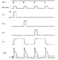
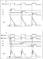
- FIG. 1 It is a figure which shows the various signal waveforms at the time of driving the display panel of the display apparatus which concerns on one Embodiment of this invention. It is a figure which shows the whole structure of a display apparatus.
- A is a figure which shows the internal structure of a signal line drive circuit, especially an output part
- b is a figure which shows the waveform of an AMP_Enable signal. It is a figure which shows simply the circuit structure of a display panel. It is a figure which shows partially the structure of the display apparatus provided with the analog amplifier of the number of gradations.
- FIG. 1 is a diagram showing a state in which the data signal line is electrically floating in the non-scanning period
- (b) is a state in which the data signal line is connected to a common voltage source in the non-scanning period.
- FIG. It is a figure which shows various signal waveforms in case a data signal line is connected to the common voltage source in a non-scanning period.
- (A) is a figure which shows various signal waveforms in case the timing which returns an analog amplifier from a non-operation state to an operation state, and the timing which turns on the gate of TFT are the same.
- (B) is a diagram showing various signal waveforms when the timing of turning on the gate of the TFT is later than the timing of returning the analog amplifier from the non-operating state to the operating state.
- (A) is a figure which shows the structure of the signal line drive circuit provided with the 1st analog amplifier group which consists of several analog amplifiers, and the 2nd analog amplifier group which consists of several analog amplifiers.
- (B) shows a configuration of a first signal line driving circuit including a first analog amplifier group including a plurality of analog amplifiers, and a second signal including a second analog amplifier group including a plurality of analog amplifiers. It is a figure which shows the structure of a line drive circuit.
- FIG. 1 is a figure which shows the various signal waveform in the case of switching to a working state from a non-operation state simultaneously to all the analog amplifiers.
- B shows various signal waveforms when the timing for switching a part of all analog amplifiers from the non-operating state to the operating state is different from the timing for switching the remaining part from the non-operating state to the operating state.
- FIG. It is a figure which shows the signal waveform at the time of the conventional display apparatus driving a display panel.
- FIG. 2 is a diagram illustrating an overall configuration of the display device 1.
- a display device 1 includes a display panel 2, a scanning line driving circuit (gate driver) 4, a signal line driving circuit (source driver) 6, a common electrode driving circuit 8, a timing controller 10, and a power generation circuit. 13 is provided.
- the timing controller 10 further includes a control signal output unit (capability control means) 12.
- the display panel 2 includes a screen composed of a plurality of pixels arranged in a matrix, and N scanning signal lines G (gate lines) for selecting and scanning the screen in a line-sequential manner. And M (M is an arbitrary integer) data signal lines S (source lines) that supply data signals to pixels of one row included in the selected line.
- the scanning signal line G and the data signal line S are orthogonal to each other.
- G (n) shown in FIG. 1 represents the n-th scanning signal line G (n is an arbitrary integer).
- G (1), G (2), and G (3) represent the first, second, and third scanning signal lines G, respectively.
- S (i) represents the i-th data signal line S (i is an arbitrary integer).
- S (1), S (2), and S (3) represent the first, second, and third data signal lines S, respectively.
- the scanning line driving circuit 4 scans each scanning signal line G line-sequentially from the top to the bottom of the screen. At this time, a rectangular wave for turning on a switching element (TFT) provided in the pixel and connected to the pixel electrode is output to each scanning signal line G. Thereby, the pixels for one row in the screen are selected.
- TFT switching element
- the signal line drive circuit 6 calculates the value of the voltage to be output to each pixel for the selected row from the input video signal (arrow A), and supplies the voltage of that value to each data signal line S. Output. As a result, image data is supplied to each pixel on the selected scanning signal line G.
- the display device 1 includes a common electrode (not shown) provided for each pixel in the screen.
- the common electrode driving circuit 8 outputs a predetermined common voltage for driving the common electrode to the common electrode based on a signal (arrow B) input from the timing controller 10.
- the timing controller 10 outputs a reference signal for each circuit to operate in synchronization with each circuit based on the input horizontal synchronization signal Hsync (arrow D). Specifically, a gate start pulse signal and a gate clock signal are output to the scanning line driving circuit 4 (arrow E). A source start pulse signal, a source latch strobe signal, and a source clock signal are output to the signal line driving circuit 6 (arrow F).
- the scanning line driving circuit 4 starts scanning the display panel 2 with a gate start pulse signal received from the timing controller 10 as a cue, and sequentially applies a selection voltage to each scanning signal line G in accordance with the gate clock signal.
- the signal line drive circuit 6 stores the input image data of each pixel in a register in accordance with the source clock signal, and each of the display panels 2 in accordance with the next source latch strobe signal. Image data is written to the data signal line S.
- the power supply generation circuit 13 generates Vdd, Vdd2, Vcc, Vgh, and Vgl, which are voltages necessary for each circuit in the display device 1 to operate. Then, Vcc, Vgh, and Vgl are output to the scanning line driving circuit 4, Vdd and Vcc are output to the signal line driving circuit 6, Vcc is output to the timing controller 10, and Vdd 2 is output to the common electrode driving circuit 8.
- a problem of power consumption in a conventional display device will be described.
- a display device having a general resolution WSVGA (1024 RGB ⁇ 600) is taken as an example.
- Each analog amplifier is an element that outputs a data signal to a data signal line.
- a constant current of about 0.01 mA flows to ensure output capability.
- Vdd voltage source supplied to the signal line driver circuit
- the display device 1 of the present embodiment operates with less power than the conventional display device described above. This point will be described with reference to FIG.
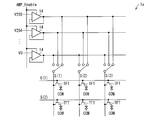
- FIG. 3 is a diagram showing an internal configuration of the signal line driving circuit 6, particularly an output portion.
- the signal line driving circuit 6 includes a plurality of analog amplifiers 14. Each analog amplifier 14 is provided for each data signal line S. Therefore, the signal line driving circuit 6 according to the present embodiment includes M analog amplifiers 14. That is, the number of analog amplifiers 14 and the number of data signal lines S are equal to each other.
- the signal line drive circuit 6 further includes an AMP_Enable signal line for inputting an AMP_Enable signal to each analog amplifier 14. This signal line is connected to the control signal output unit 12 of the timing controller 10. In addition, the signal line driving circuit 6 is connected in parallel to each analog amplifier 14.
- Vdd is a voltage source supplied from the power supply generation circuit 13 in the display device 1 and is used to operate each circuit in the display device 1 including the signal line drive circuit 6.
- Each analog amplifier 14 also operates upon receiving Vdd.
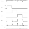
- the control signal output unit 12 of the timing controller 10 outputs an AMP_Enable signal, which is a control signal that defines the operating state of each analog amplifier 14, to each analog amplifier 14 of the signal line drive circuit 6 at a predetermined timing. Specifically, as shown in FIG. 3B, the control signal output unit 12 sets the voltage of the AMP_Enable signal to the H value (high value) in accordance with the timing at which a certain horizontal synchronization signal Hsync is output, Thereafter, the voltage of the AMP_Enable signal is set to the L value (low value) until the next horizontal synchronization signal Hsync becomes H.
- the analog amplifier 14 operates when the AMP_Enable signal is at the H value and pauses when the AMP_Enable signal is at the L value.
- the display device 1 displays an image of 60 frames per second on the display panel 2. Therefore, one frame period is about 16.7 ms. Since the resolution of the display device 1 is 1024 ⁇ 600 pixels, 600 scanning signal lines G are scanned during one frame period. When the vertical blanking period is 5 horizontal periods, one horizontal period is about 27.5 us.
- the display device 1 When driving the display panel 2, the display device 1 divides one horizontal period into a scanning period and a non-scanning period.
- the analog amplifier 14 is operated by setting the AMP_Enable signal to the H value. Further, the scanning signal is set to Vgh to turn on the TFT gate.
- the scanning period is equal to the time required for the voltage required for display to be written into the pixel electrode. In this embodiment, the scanning period occupies about one third of one horizontal period.
- the display device 1 sets the AMP_Enable signal to the L value and pauses the analog amplifier 14. Further, the scanning signal is set to Vgl to turn off the TFT gate. Since the non-scanning period is a period other than the scanning period in one horizontal period, this embodiment occupies about two-thirds of one horizontal period.
- FIG. 4 is a diagram schematically showing the circuit structure of the display panel 2. As shown in this figure, each pixel in the display panel 2 is provided with a TFT, and the drain of the TFT is connected to a pixel electrode (not shown). The display panel 2 is provided with a common electrode (COM) so as to face the pixel electrode and sandwich the liquid crystal layer.
- COM common electrode
- FIG. 1 is a diagram showing various signal waveforms when driving the display panel 2 of the display device 1 according to an embodiment of the present invention.
- Hsync is input every horizontal period.
- the voltage of the AMP_Enable signal is changed from the H value to the L value.
- the analog amplifier 14 included in the signal line driving circuit 6 is switched from the non-operating state to the operating state (normal state).
- the AMP_Enable signal maintains the H value while a voltage necessary for display is continuously applied to the data signal line S (i).
- the AMP_Enable signal is changed from the H value to the L value within one horizontal period.
- the analog amplifier 14 becomes inactive.
- the connection between the output of the analog amplifier 14 and the data signal line S (i) is disconnected.
- the data signal line S (i) may be in an electrically floating state or connected to Vdd or the like. Since the voltage waveform of the data signal line S (i) is determined according to the state at that time, in FIG. 1, it is indicated by a dotted line indicating a waveform that is not fixed, not a solid line that indicates a fixed waveform. Since the voltage necessary for display is already applied to the pixel electrode, the display is not greatly affected.
- the time required to complete the application of the voltage necessary for display is mainly determined according to the characteristics of the TFT. Therefore, the time may be calculated based on the design value of the TFT and stored in the display device 1 for use. In this embodiment, the time is one third of one horizontal period.
- the gate voltage is changed from Vgh to Vgl. Thereby, the gate of the TFT returns from the on state to the off state.
- the next Hsync is input.
- the pixels for one row connected to the second and subsequent scanning signal lines G are driven by the same procedure as the pixels for one row connected to the first scanning signal line G.
- the display device 1 drives the display panel 2 to invert the polarity, the polarity of the voltage applied to the data signal line S (i) is inverted every time the scanning signal line G to be scanned changes.
- the first scanning signal line G (1) is scanned, a data signal that changes from the negative electrode to the positive electrode is applied to the data signal line S (i), and the second scanning signal line G (2). Is scanned, the data signal changing from the positive electrode to the negative electrode is applied to the data signal line S (i).
- the display device 1 is a display device including the signal line driving circuit 6 provided with a circuit (analog amplifier 14) through which a steady current flows, and in one horizontal period, the data signal line S (i).
- the steady current of the analog amplifier 14 is cut from the start time to the end time in the non-scanning period (that is, the non-scanning period).
- the average current consumption becomes a value indicated by an arrow P in FIG. 1, and this value is significantly smaller than the average current consumption in the conventional display device (arrow P ′ in FIG. 11). Therefore, the display device 1 has an effect of reducing power consumption compared to the conventional display device.
- the period during which the analog amplifier 14 is stopped is completed within one horizontal period. Specifically, the analog amplifier 14 is always in an operating state every horizontal period, and a voltage necessary for display is output to each data signal line S (i). Thereby, the refresh period of each pixel becomes equal to one frame period. In other words, the image is refreshed in all frame periods. As a result, since the image refresh frequency is not lowered, a smooth moving image can be displayed.
- FIG. 11 is a diagram illustrating signal waveforms when a conventional display device drives a display panel. As shown in this figure, in the conventional display device, each analog amplifier maintains the operating state for one horizontal period. Further, the gate voltage maintains the H value for one horizontal period (maintains the gate-on state).
- the conventional display device In the conventional display device, a steady current always flows in the analog amplifier during one horizontal period. That is, control for cutting the steady current is not performed in a specific period within one horizontal period. As a result, the average current consumption becomes a value indicated by an arrow P 'in FIG. Thus, unlike the display device 1 of the present invention, the conventional display device does not have the effect of reducing power consumption.
- the number of analog amplifiers 14 and the number of data signal lines S are not necessarily the same.
- the number can be smaller than the number of data signal lines S. This example will be described below with reference to FIG.
- FIG. 5 is a diagram partially showing a configuration of the display device 1a including the analog amplifier 14 having the number of gradations.
- the signal line drive circuit 6 of the display device 1 a includes 256 analog amplifiers (gradation) 14.
- Each analog amplifier 14 outputs V0 to V255, which is a voltage for displaying any gradation of 0 to 255, to the data signal line S (i).
- the output voltage is predetermined for each analog amplifier 14, and there is only one analog amplifier 14 that outputs the same voltage.
- each analog amplifier 14 can be connected to all the data signal lines S in the display panel 2. Therefore, the same voltage can be output from one analog amplifier 14 to any number of data signal lines S.
- the data signal line S (i) connected to the pixel on the selected scanning signal line G is connected to the analog amplifier 14 that outputs a voltage corresponding to the gradation displayed by the pixel. .
- Each analog amplifier 14 can receive the above-described AMP_Enable signal. Therefore, the driving method described with reference to FIG. 1 can also be executed by the display device 1 shown in FIG. That is, since 256 analog amplifiers 14 are all in the non-operating state in the non-scanning period within one horizontal period, the steady current in the non-scanning period can be reduced, and as a result, the power consumption can be reduced.
- connection destination of the data signal line S (i) may be indefinite or an arbitrary power source.
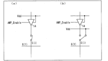
- FIG. 6 is a diagram showing a state in which the data signal line S (i) is electrically floating in the non-scanning period.
- the connection between the analog amplifier 14 and the data signal line S (i) is disconnected during the non-scanning period (the period in which the AMP_Enable signal is L value), and the data signal line S (i) is disconnected.
- the connection destination is undefined. That is, the data signal line S (i) is electrically floating.
- FIG. 6 is a diagram showing a state in which the data signal line S (i) is connected to the common Vdd in the non-scanning period.
- FIG. 7 is a diagram showing various signal waveforms when the data signal line S (i) is connected to a common pressure power supply in the non-scanning period.
- Vdd common voltage source
- the voltage output to the data signal line S (i) decreases by a certain value from the peak value after the end of the scanning period, that is, after the AMP_Enable signal changes from the H value to the L value. Keep stable (arrow Q in FIG. 7). As a result, since the voltage output to the data signal line S is stabilized in the non-scanning period, stable display can be maintained.
- connection destination of the data signal line S (i) in the non-scanning period is not limited to an arbitrary voltage source (Vdd), and may be a ground (GND) or a common node. In either case, the effect of stabilizing the voltage output to the data signal line S in the non-scanning period can be obtained.
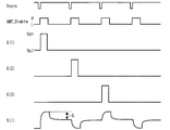
- (Example of shifting the timing) (A) in FIG. 8 is a diagram showing various signal waveforms when the timing at which the analog amplifier 14 is returned from the non-operating state to the operating state is the same as the timing at which the TFT gate is turned on. (B) in FIG. 8 is a diagram showing various signal waveforms when the timing at which the gate of the TFT is turned on is later than the timing at which the analog amplifier 14 is returned from the non-operating state to the operating state.
- the analog amplifier 14 when the analog amplifier 14 is returned from the non-operating state to the operating state, a certain amount of time is required until the analog amplifier 14 can operate normally. Therefore, when the timing for returning the analog amplifier 14 and the timing for turning on the TFT gate are the same, the signal output from the analog amplifier 14 to the data signal line S in the period K in FIG. This state becomes unstable as indicated by 30 in FIG. As a result, there is a possibility that an originally unintended voltage may be applied to the pixel.
- the timing at which the TFT gate is turned on (that is, the scan signal is changed from Vgl to Vgh) may be delayed from the timing at which the analog amplifier 14 is returned from the non-operating state to the operating state.
- the period T0 in FIG. 8B that is, the time from when the AMP_Enable signal is changed from the L value to the H value until the time when the scanning signal is changed from Vgl to Vgh, is from 0 us. Also set a larger value.
- the gate of the TFT is turned on after the time until the analog amplifier 14 recovers from the non-operating state and stabilizes. As a result, a normal voltage can be applied to the pixel.
- all the analog amplifiers 14 may be divided into a plurality of analog amplifier groups and switched from the non-operating state to the operating state at different timings for each analog amplifier group. This example will be described with reference to FIG. 9 and FIG.
- FIG. 9A is a diagram illustrating a configuration of a signal line driving circuit 6a including an analog amplifier group 20 including a plurality of analog amplifiers 14 and an analog amplifier group 21 including a plurality of analog amplifiers 14.
- FIG. 9B shows the configuration of the signal line driving circuit 6b including the analog amplifier group 20 including the plurality of analog amplifiers 14, and the signal line driving circuit including the analog amplifier group 21 including the plurality of analog amplifiers 14.
- FIG. It is a figure which shows the structure of 6c.
- the display device 1 includes one signal line driving circuit 6a. All the analog amplifiers 14 are divided into two analog amplifier groups 20 and 21 in the signal line driving circuit 6a.
- the display device 1 includes two signal line drive circuits 6b and 6c. The plurality of analog amplifiers 14 form one analog amplifier group 20 in the signal line drive circuit 6b. On the other hand, the plurality of analog amplifiers 14 form one analog amplifier group 21 in the signal line driving circuit 6c.
- the analog amplifier group 20 is controlled by the AMP_Enable1 signal
- the analog amplifier group 21 is controlled by the AMP_Enable2 signal.
- FIG. 10 is a diagram showing various signal waveforms when all analog amplifiers 14 are simultaneously switched from the non-operating state to the operating state.
- (B) in FIG. 10 is a case where the timing for switching a part of all the analog amplifiers 14 from the non-operating state to the operating state is different from the timing for switching the remaining part from the non-operating state to the operating state. It is a figure which shows various signal waveforms.
- the analog amplifier 14 when the analog amplifier 14 is switched from the non-operating state to the operating state, an inrush current flows through the power line of the analog amplifier 14. If all the analog amplifiers 14 are switched to the operating state at the same time, the inrush current is doubled by the number of analog amplifiers 14, so that a large inrush current flows to the power supply line as shown in FIG. As a result, the power supply may drop.
- the control shown in (b) in FIG. 10 is possible.
- the AMP_Enable2 signal is switched from the L value to the H value after the period T1 has elapsed after the AMP_Enable1 signal is switched from the L value to the H value.
- the scanning signal is switched from Vgl to Vgh.
- the start point of the non-scanning period is not limited to immediately after the application of the voltage necessary for display is completed, but may be a little after the end point.
- the end point of the non-scanning period is not limited to the time point when one horizontal period ends, and is not limited to a little before that. That is, a period of any length between the end of the scanning period and the end of one horizontal synchronization period can be a non-scanning period.
- analog amplifier 14 that is the target of operation suspension during the non-scanning period. That is, the capability of any circuit group (element group) including the analog amplifier 14 through which steady current flows may be reduced.
- Examples of such a circuit group include a DAC (Digital-Analogue-Converter) circuit unit that determines a voltage for each gradation and a Vdd generation circuit unit.
- DAC Digital-Analogue-Converter
- the display device 1 can reduce power consumption by reducing the capability (driving capability) of the analog amplifier 14 during the non-scanning period as described above. However, it is possible to maximize the effect of reducing power consumption by completely stopping the analog amplifier 14 (Off). Therefore, in the display device 1, the effect of the present invention can also be achieved by “suspending the analog amplifier 14” instead of “decreasing the driving capability of the analog amplifier 14” in the non-scanning period. Note that the state in which the ability of the analog amplifier 14 is most reduced corresponds to the state in which the analog amplifier 14 is stopped.
- the circuit through which the steady current flows is a plurality of analog amplifiers that output a data signal voltage to the data signal line, It is preferable that the capability control means reduces the capability of at least one of the plurality of analog amplifiers between the start time and the end time.
- the constantly steady current flowing through the analog amplifier can be reduced in the non-scanning period.
- the capability control means decreases the capabilities of all the analog amplifiers from the start time to the end time.
- the display device preferably further includes a scanning line driving circuit that outputs a signal for turning off the gate of the switching element connected to the pixel electrode at the start time.
- the plurality of analog amplifiers are divided into a plurality of analog amplifier groups each consisting of a plurality of analog amplifiers, It is preferable that the capability control means restores the plurality of analog amplifiers included in the analog amplifier from a state in which the capability is reduced to a normal state at a timing different for each analog amplifier group.
- the peak value of the inrush current generated when the analog amplifier returns to the normal state can be reduced.
- the start time is preferably immediately after the application of the voltage necessary for the display is completed.
- the end point is preferably a point at which the one horizontal period ends.
- the capability control means returns the circuit through which the steady current flows to a normal state at the end time, It is preferable to further include a scanning line driving circuit that outputs a signal for turning on the gate of the switching element connected to the pixel electrode after the end point.
- the gate of the switching element is turned on after the time until the circuit through which the steady current flows returns from the low-capacity state and stabilizes. As a result, a normal voltage can be applied to the pixel.
- the capability control means preferably changes the connection destination of the data signal line from the analog amplifier to an arbitrary voltage source between the start time and the end time.
- the voltage output to the data signal line is stabilized in the non-scanning period, so that stable display can be maintained.
- the display device is a liquid crystal display device.
- a liquid crystal display device capable of displaying a moving image without causing flicker and reducing power consumption is realized.
- the display device according to the present invention can be widely used as various display devices such as liquid crystal display devices, organic EL display devices, and electronic paper.
Landscapes
- Engineering & Computer Science (AREA)
- Chemical & Material Sciences (AREA)
- Crystallography & Structural Chemistry (AREA)
- Physics & Mathematics (AREA)
- Computer Hardware Design (AREA)
- General Physics & Mathematics (AREA)
- Theoretical Computer Science (AREA)
- Control Of Indicators Other Than Cathode Ray Tubes (AREA)
- Liquid Crystal Display Device Control (AREA)
- Liquid Crystal (AREA)
Abstract
Priority Applications (4)
| Application Number | Priority Date | Filing Date | Title |
|---|---|---|---|
| EP10847062.6A EP2544169A4 (fr) | 2010-03-03 | 2010-12-13 | Dispositif d'affichage, son procédé de commande et dispositif d'affichage à cristaux liquides |
| JP2012502967A JP5734951B2 (ja) | 2010-03-03 | 2010-12-13 | 表示装置およびその駆動方法、ならびに液晶表示装置 |
| US13/581,538 US9076405B2 (en) | 2010-03-03 | 2010-12-13 | Display device, method for driving same, and liquid crystal display device |
| CN201080065108.9A CN102792358B (zh) | 2010-03-03 | 2010-12-13 | 显示装置及其驱动方法、以及液晶显示装置 |
Applications Claiming Priority (2)
| Application Number | Priority Date | Filing Date | Title |
|---|---|---|---|
| JP2010-046789 | 2010-03-03 | ||
| JP2010046789 | 2010-03-03 |
Publications (1)
| Publication Number | Publication Date |
|---|---|
| WO2011108166A1 true WO2011108166A1 (fr) | 2011-09-09 |
Family
ID=44541838
Family Applications (1)
| Application Number | Title | Priority Date | Filing Date |
|---|---|---|---|
| PCT/JP2010/072383 WO2011108166A1 (fr) | 2010-03-03 | 2010-12-13 | Dispositif d'affichage, son procédé de commande et dispositif d'affichage à cristaux liquides |
Country Status (5)
| Country | Link |
|---|---|
| US (1) | US9076405B2 (fr) |
| EP (1) | EP2544169A4 (fr) |
| JP (1) | JP5734951B2 (fr) |
| CN (1) | CN102792358B (fr) |
| WO (1) | WO2011108166A1 (fr) |
Cited By (5)
| Publication number | Priority date | Publication date | Assignee | Title |
|---|---|---|---|---|
| WO2012137817A1 (fr) * | 2011-04-08 | 2012-10-11 | シャープ株式会社 | Dispositif d'affichage et procédé de commande d'un dispositif d'affichage |
| JPWO2011145360A1 (ja) * | 2010-05-21 | 2013-07-22 | シャープ株式会社 | 表示装置およびその駆動方法、ならびに表示システム |
| KR20140129622A (ko) * | 2013-04-30 | 2014-11-07 | 엘지디스플레이 주식회사 | 저속 구동용 표시장치와 그 구동방법 |
| JP5889421B2 (ja) * | 2012-09-26 | 2016-03-22 | シャープ株式会社 | 表示装置およびその駆動方法 |
| CN110751930A (zh) * | 2018-01-22 | 2020-02-04 | 青岛海信移动通信技术股份有限公司 | 用于墨水屏的页面刷新方法及装置 |
Families Citing this family (6)
| Publication number | Priority date | Publication date | Assignee | Title |
|---|---|---|---|---|
| US9293103B2 (en) * | 2011-04-07 | 2016-03-22 | Sharp Kabushiki Kaisha | Display device, and method for driving same |
| DE112013007187B4 (de) * | 2013-09-13 | 2023-08-10 | Ev Group E. Thallner Gmbh | Verfahren zum Aufbringen einer Bondschicht |
| US20160284281A1 (en) * | 2013-11-01 | 2016-09-29 | Sharp Kabushiki Kaisha | Display apparatus and control device |
| JP2015090414A (ja) * | 2013-11-06 | 2015-05-11 | シナプティクス・ディスプレイ・デバイス株式会社 | 表示駆動回路および表示装置 |
| JP2016192665A (ja) * | 2015-03-31 | 2016-11-10 | ラピスセミコンダクタ株式会社 | 半導体装置 |
| US20210238558A1 (en) * | 2018-06-01 | 2021-08-05 | Medicenna Therapeutics, Inc. | Uses and methods for oncolytic virus targeting of il-4/il-13 and fusions thereof |
Citations (8)
| Publication number | Priority date | Publication date | Assignee | Title |
|---|---|---|---|---|
| JP2001312253A (ja) | 2000-04-28 | 2001-11-09 | Sharp Corp | 表示装置の駆動方法およびそれを用いた表示装置ならびに携帯機器 |
| JP2002182619A (ja) * | 2000-10-05 | 2002-06-26 | Sharp Corp | 表示装置の駆動方法およびそれを用いた表示装置 |
| JP2002215108A (ja) * | 2001-01-16 | 2002-07-31 | Nec Corp | 液晶ディスプレイの駆動方法、その回路及び携帯用電子機器 |
| JP2003330429A (ja) * | 2002-05-14 | 2003-11-19 | Nec Kansai Ltd | 液晶表示用駆動回路の出力回路 |
| JP2005165102A (ja) * | 2003-12-04 | 2005-06-23 | Nec Electronics Corp | 表示装置、その駆動回路およびその駆動方法 |
| JP2008176159A (ja) * | 2007-01-22 | 2008-07-31 | Hitachi Displays Ltd | 表示装置 |
| JP2008224798A (ja) * | 2007-03-09 | 2008-09-25 | Renesas Technology Corp | 表示用駆動回路 |
| JP2009216853A (ja) * | 2008-03-10 | 2009-09-24 | Epson Imaging Devices Corp | 電気光学装置及び電子機器 |
Family Cites Families (25)
| Publication number | Priority date | Publication date | Assignee | Title |
|---|---|---|---|---|
| US5307212A (en) * | 1991-08-22 | 1994-04-26 | Rohm Co., Ltd. | Trapezoidal wave generation in a video control signal write circuit |
| KR0140041B1 (ko) * | 1993-02-09 | 1998-06-15 | 쯔지 하루오 | 표시 장치용 전압 발생 회로, 공통 전극 구동 회로, 신호선 구동 회로 및 계조 전압 발생 회로 |
| US5798747A (en) * | 1995-11-17 | 1998-08-25 | National Semiconductor Corporation | Methods and apparatuses for high-speed video sample and hold amplification for analog flat panel display |
| US7304632B2 (en) * | 1997-05-13 | 2007-12-04 | Oki Electric Industry Co., Ltd. | Liquid-crystal display driving circuit and method |
| EP1296174B1 (fr) | 2000-04-28 | 2016-03-09 | Sharp Kabushiki Kaisha | Unite d'affichage, procede d'excitation pour unite d'affichage, et appareil electronique de montage d'une unite d'affichage |
| JP4868652B2 (ja) * | 2001-04-11 | 2012-02-01 | 三洋電機株式会社 | 表示装置 |
| JP4532773B2 (ja) * | 2001-04-13 | 2010-08-25 | キヤノン株式会社 | 電子回路、及び該電子回路を備えた液晶装置 |
| EP2148317B1 (fr) * | 2001-08-29 | 2018-06-20 | Gold Charm Limited | Dispositif semi-conducteur pour attaquer un dispositif à charge de courant et dispositif à charge de courant comportant ce dispositif semi-conducteur |
| JP4372392B2 (ja) * | 2001-11-30 | 2009-11-25 | ティーピーオー ホンコン ホールディング リミテッド | 列電極駆動回路及びこれを用いた表示装置 |
| JP4225777B2 (ja) * | 2002-02-08 | 2009-02-18 | シャープ株式会社 | 表示装置ならびにその駆動回路および駆動方法 |
| JP4094328B2 (ja) * | 2002-04-10 | 2008-06-04 | シャープ株式会社 | 表示装置駆動回路および表示装置駆動回路の駆動方法 |
| JP2004117742A (ja) * | 2002-09-25 | 2004-04-15 | Sharp Corp | 表示装置ならびにその駆動回路および駆動方法 |
| JP3922176B2 (ja) * | 2002-12-24 | 2007-05-30 | 株式会社日立製作所 | 表示装置用駆動電源回路 |
| JP2005010282A (ja) * | 2003-06-17 | 2005-01-13 | Mitsubishi Electric Corp | 画像表示装置 |
| JP2005017771A (ja) * | 2003-06-26 | 2005-01-20 | Nec Micro Systems Ltd | マトリクス型表示装置 |
| KR101165842B1 (ko) | 2005-06-30 | 2012-07-13 | 엘지디스플레이 주식회사 | 모바일용 액정 표시 장치 및 그 구동 방법 |
| JP2008040195A (ja) | 2006-08-08 | 2008-02-21 | Seiko Epson Corp | 対向電極電圧生成回路、ソースドライバ、電気光学装置及び電子機器 |
| CN101872585B (zh) | 2007-01-22 | 2013-07-17 | 株式会社日立显示器 | 显示装置 |
| JP2008298997A (ja) * | 2007-05-30 | 2008-12-11 | Toshiba Matsushita Display Technology Co Ltd | 表示装置及び表示装置の駆動方法 |
| JP5319100B2 (ja) * | 2007-10-31 | 2013-10-16 | ローム株式会社 | ソースドライバおよびそれを用いた液晶ディスプレイ装置 |
| KR101581170B1 (ko) * | 2008-03-31 | 2016-01-12 | 삼성디스플레이 주식회사 | 백라이트 구동 방법과 백라이트 구동 장치 및 이를포함하는 표시 장치 |
| JP5356208B2 (ja) * | 2009-12-25 | 2013-12-04 | 株式会社ジャパンディスプレイ | ゲート信号線駆動回路及び表示装置 |
| JP2011150256A (ja) * | 2010-01-25 | 2011-08-04 | Renesas Electronics Corp | 駆動回路及び駆動方法 |
| BR112012029386A2 (pt) * | 2010-05-21 | 2016-07-26 | Sharp Kk | dispositivo de vídeo, método de acionamento de dispositivo de vídeo, e sistema de vídeo |
| US9147372B2 (en) * | 2011-03-31 | 2015-09-29 | Sharp Kabushiki Kaisha | Display device |
-
2010
- 2010-12-13 EP EP10847062.6A patent/EP2544169A4/fr not_active Withdrawn
- 2010-12-13 JP JP2012502967A patent/JP5734951B2/ja not_active Expired - Fee Related
- 2010-12-13 US US13/581,538 patent/US9076405B2/en not_active Expired - Fee Related
- 2010-12-13 WO PCT/JP2010/072383 patent/WO2011108166A1/fr active Application Filing
- 2010-12-13 CN CN201080065108.9A patent/CN102792358B/zh not_active Expired - Fee Related
Patent Citations (8)
| Publication number | Priority date | Publication date | Assignee | Title |
|---|---|---|---|---|
| JP2001312253A (ja) | 2000-04-28 | 2001-11-09 | Sharp Corp | 表示装置の駆動方法およびそれを用いた表示装置ならびに携帯機器 |
| JP2002182619A (ja) * | 2000-10-05 | 2002-06-26 | Sharp Corp | 表示装置の駆動方法およびそれを用いた表示装置 |
| JP2002215108A (ja) * | 2001-01-16 | 2002-07-31 | Nec Corp | 液晶ディスプレイの駆動方法、その回路及び携帯用電子機器 |
| JP2003330429A (ja) * | 2002-05-14 | 2003-11-19 | Nec Kansai Ltd | 液晶表示用駆動回路の出力回路 |
| JP2005165102A (ja) * | 2003-12-04 | 2005-06-23 | Nec Electronics Corp | 表示装置、その駆動回路およびその駆動方法 |
| JP2008176159A (ja) * | 2007-01-22 | 2008-07-31 | Hitachi Displays Ltd | 表示装置 |
| JP2008224798A (ja) * | 2007-03-09 | 2008-09-25 | Renesas Technology Corp | 表示用駆動回路 |
| JP2009216853A (ja) * | 2008-03-10 | 2009-09-24 | Epson Imaging Devices Corp | 電気光学装置及び電子機器 |
Non-Patent Citations (1)
| Title |
|---|
| See also references of EP2544169A4 |
Cited By (9)
| Publication number | Priority date | Publication date | Assignee | Title |
|---|---|---|---|---|
| JPWO2011145360A1 (ja) * | 2010-05-21 | 2013-07-22 | シャープ株式会社 | 表示装置およびその駆動方法、ならびに表示システム |
| WO2012137817A1 (fr) * | 2011-04-08 | 2012-10-11 | シャープ株式会社 | Dispositif d'affichage et procédé de commande d'un dispositif d'affichage |
| JP5399586B2 (ja) * | 2011-04-08 | 2014-01-29 | シャープ株式会社 | 表示装置 |
| JP5889421B2 (ja) * | 2012-09-26 | 2016-03-22 | シャープ株式会社 | 表示装置およびその駆動方法 |
| JPWO2014050291A1 (ja) * | 2012-09-26 | 2016-08-22 | シャープ株式会社 | 表示装置およびその駆動方法 |
| KR20140129622A (ko) * | 2013-04-30 | 2014-11-07 | 엘지디스플레이 주식회사 | 저속 구동용 표시장치와 그 구동방법 |
| KR102050380B1 (ko) | 2013-04-30 | 2019-11-29 | 엘지디스플레이 주식회사 | 저속 구동용 표시장치와 그 구동방법 |
| CN110751930A (zh) * | 2018-01-22 | 2020-02-04 | 青岛海信移动通信技术股份有限公司 | 用于墨水屏的页面刷新方法及装置 |
| CN110751930B (zh) * | 2018-01-22 | 2021-05-18 | 青岛海信移动通信技术股份有限公司 | 用于墨水屏的页面刷新方法及装置 |
Also Published As
| Publication number | Publication date |
|---|---|
| EP2544169A4 (fr) | 2015-04-22 |
| US9076405B2 (en) | 2015-07-07 |
| EP2544169A1 (fr) | 2013-01-09 |
| JPWO2011108166A1 (ja) | 2013-06-20 |
| JP5734951B2 (ja) | 2015-06-17 |
| US20130009935A1 (en) | 2013-01-10 |
| CN102792358B (zh) | 2015-03-25 |
| CN102792358A (zh) | 2012-11-21 |
Similar Documents
| Publication | Publication Date | Title |
|---|---|---|
| JP5734951B2 (ja) | 表示装置およびその駆動方法、ならびに液晶表示装置 | |
| US11056049B2 (en) | Display device | |
| WO2012057044A1 (fr) | Dispositif d'affichage, son procédé d'affichage et dispositif d'affichage à cristaux liquides | |
| JP3744826B2 (ja) | 表示制御回路、電気光学装置、表示装置及び表示制御方法 | |
| JP5819407B2 (ja) | 表示装置およびその駆動方法 | |
| WO2011145360A1 (fr) | Dispositif d'affichage et procédé de commande associé, et système d'affichage | |
| KR102527847B1 (ko) | 표시 장치 | |
| JP4510530B2 (ja) | 液晶表示装置とその駆動方法 | |
| JP5373209B2 (ja) | 表示装置および駆動方法 | |
| US11195468B2 (en) | Display apparatus and method of driving display panel using the same | |
| TWI537926B (zh) | 顯示裝置及其驅動方法 | |
| KR100465471B1 (ko) | 표시 장치 | |
| JP4786897B2 (ja) | ソース駆動回路と駆動回路及び液晶ディスプレイ装置とその駆動方法 | |
| KR20160005839A (ko) | 표시장치 | |
| JP2008170842A (ja) | 電気光学装置、駆動回路および電子機器 | |
| KR101785339B1 (ko) | 공통전압 드라이버 및 이를 포함하는 액정표시장치 | |
| KR20230102585A (ko) | 게이트 구동 회로 및 이를 이용한 표시 장치 | |
| JP3882844B2 (ja) | 表示制御回路、電気光学装置、表示装置及び表示制御方法 | |
| JP4674985B2 (ja) | 液晶表示装置ならびにそれを備える携帯電話機および携帯情報端末機器 | |
| JP2008158385A (ja) | 電気光学装置、その駆動方法および電子機器 | |
| US20230419904A1 (en) | Display panel, method for driving a display panel and display apparatus | |
| JP2009075298A (ja) | 電気光学装置、駆動回路、駆動方法および電子機器 | |
| WO2011077825A1 (fr) | Dispositif d'affichage à cristaux liquides, procédé d'attaque de dispositif d'affichage à cristaux liquides et dispositif électronique |
Legal Events
| Date | Code | Title | Description |
|---|---|---|---|
| WWE | Wipo information: entry into national phase |
Ref document number: 201080065108.9 Country of ref document: CN |
|
| 121 | Ep: the epo has been informed by wipo that ep was designated in this application |
Ref document number: 10847062 Country of ref document: EP Kind code of ref document: A1 |
|
| WWE | Wipo information: entry into national phase |
Ref document number: 2012502967 Country of ref document: JP |
|
| WWE | Wipo information: entry into national phase |
Ref document number: 2010847062 Country of ref document: EP |
|
| WWE | Wipo information: entry into national phase |
Ref document number: 13581538 Country of ref document: US |
|
| NENP | Non-entry into the national phase |
Ref country code: DE |