WO2011105282A1 - 配線形成方法、および、半導体基板の製造方法 - Google Patents
配線形成方法、および、半導体基板の製造方法 Download PDFInfo
- Publication number
- WO2011105282A1 WO2011105282A1 PCT/JP2011/053406 JP2011053406W WO2011105282A1 WO 2011105282 A1 WO2011105282 A1 WO 2011105282A1 JP 2011053406 W JP2011053406 W JP 2011053406W WO 2011105282 A1 WO2011105282 A1 WO 2011105282A1
- Authority
- WO
- WIPO (PCT)
- Prior art keywords
- film
- wiring
- etching
- insulating film
- metal
- Prior art date
- Legal status (The legal status is an assumption and is not a legal conclusion. Google has not performed a legal analysis and makes no representation as to the accuracy of the status listed.)
- Ceased
Links
Images





Classifications
-
- H—ELECTRICITY
- H10—SEMICONDUCTOR DEVICES; ELECTRIC SOLID-STATE DEVICES NOT OTHERWISE PROVIDED FOR
- H10P—GENERIC PROCESSES OR APPARATUS FOR THE MANUFACTURE OR TREATMENT OF DEVICES COVERED BY CLASS H10
- H10P50/00—Etching of wafers, substrates or parts of devices
- H10P50/71—Etching of wafers, substrates or parts of devices using masks for conductive or resistive materials
-
- H—ELECTRICITY
- H10—SEMICONDUCTOR DEVICES; ELECTRIC SOLID-STATE DEVICES NOT OTHERWISE PROVIDED FOR
- H10D—INORGANIC ELECTRIC SEMICONDUCTOR DEVICES
- H10D30/00—Field-effect transistors [FET]
- H10D30/01—Manufacture or treatment
- H10D30/021—Manufacture or treatment of FETs having insulated gates [IGFET]
- H10D30/031—Manufacture or treatment of FETs having insulated gates [IGFET] of thin-film transistors [TFT]
- H10D30/0312—Manufacture or treatment of FETs having insulated gates [IGFET] of thin-film transistors [TFT] characterised by the gate electrodes
- H10D30/0316—Manufacture or treatment of FETs having insulated gates [IGFET] of thin-film transistors [TFT] characterised by the gate electrodes of lateral bottom-gate TFTs comprising only a single gate
-
- H—ELECTRICITY
- H10—SEMICONDUCTOR DEVICES; ELECTRIC SOLID-STATE DEVICES NOT OTHERWISE PROVIDED FOR
- H10D—INORGANIC ELECTRIC SEMICONDUCTOR DEVICES
- H10D30/00—Field-effect transistors [FET]
- H10D30/01—Manufacture or treatment
- H10D30/021—Manufacture or treatment of FETs having insulated gates [IGFET]
- H10D30/031—Manufacture or treatment of FETs having insulated gates [IGFET] of thin-film transistors [TFT]
- H10D30/0321—Manufacture or treatment of FETs having insulated gates [IGFET] of thin-film transistors [TFT] comprising silicon, e.g. amorphous silicon or polysilicon
-
- H—ELECTRICITY
- H10—SEMICONDUCTOR DEVICES; ELECTRIC SOLID-STATE DEVICES NOT OTHERWISE PROVIDED FOR
- H10D—INORGANIC ELECTRIC SEMICONDUCTOR DEVICES
- H10D30/00—Field-effect transistors [FET]
- H10D30/60—Insulated-gate field-effect transistors [IGFET]
- H10D30/67—Thin-film transistors [TFT]
- H10D30/6729—Thin-film transistors [TFT] characterised by the electrodes
- H10D30/6737—Thin-film transistors [TFT] characterised by the electrodes characterised by the electrode materials
-
- H—ELECTRICITY
- H10—SEMICONDUCTOR DEVICES; ELECTRIC SOLID-STATE DEVICES NOT OTHERWISE PROVIDED FOR
- H10D—INORGANIC ELECTRIC SEMICONDUCTOR DEVICES
- H10D30/00—Field-effect transistors [FET]
- H10D30/60—Insulated-gate field-effect transistors [IGFET]
- H10D30/67—Thin-film transistors [TFT]
- H10D30/6729—Thin-film transistors [TFT] characterised by the electrodes
- H10D30/6737—Thin-film transistors [TFT] characterised by the electrodes characterised by the electrode materials
- H10D30/6739—Conductor-insulator-semiconductor electrodes
-
- H—ELECTRICITY
- H10—SEMICONDUCTOR DEVICES; ELECTRIC SOLID-STATE DEVICES NOT OTHERWISE PROVIDED FOR
- H10D—INORGANIC ELECTRIC SEMICONDUCTOR DEVICES
- H10D30/00—Field-effect transistors [FET]
- H10D30/60—Insulated-gate field-effect transistors [IGFET]
- H10D30/67—Thin-film transistors [TFT]
- H10D30/674—Thin-film transistors [TFT] characterised by the active materials
- H10D30/6741—Group IV materials, e.g. germanium or silicon carbide
- H10D30/6743—Silicon
-
- H—ELECTRICITY
- H10—SEMICONDUCTOR DEVICES; ELECTRIC SOLID-STATE DEVICES NOT OTHERWISE PROVIDED FOR
- H10D—INORGANIC ELECTRIC SEMICONDUCTOR DEVICES
- H10D86/00—Integrated devices formed in or on insulating or conducting substrates, e.g. formed in silicon-on-insulator [SOI] substrates or on stainless steel or glass substrates
- H10D86/40—Integrated devices formed in or on insulating or conducting substrates, e.g. formed in silicon-on-insulator [SOI] substrates or on stainless steel or glass substrates characterised by multiple TFTs
- H10D86/441—Interconnections, e.g. scanning lines
-
- H—ELECTRICITY
- H10—SEMICONDUCTOR DEVICES; ELECTRIC SOLID-STATE DEVICES NOT OTHERWISE PROVIDED FOR
- H10D—INORGANIC ELECTRIC SEMICONDUCTOR DEVICES
- H10D86/00—Integrated devices formed in or on insulating or conducting substrates, e.g. formed in silicon-on-insulator [SOI] substrates or on stainless steel or glass substrates
- H10D86/40—Integrated devices formed in or on insulating or conducting substrates, e.g. formed in silicon-on-insulator [SOI] substrates or on stainless steel or glass substrates characterised by multiple TFTs
- H10D86/60—Integrated devices formed in or on insulating or conducting substrates, e.g. formed in silicon-on-insulator [SOI] substrates or on stainless steel or glass substrates characterised by multiple TFTs wherein the TFTs are in active matrices
-
- H—ELECTRICITY
- H10—SEMICONDUCTOR DEVICES; ELECTRIC SOLID-STATE DEVICES NOT OTHERWISE PROVIDED FOR
- H10P—GENERIC PROCESSES OR APPARATUS FOR THE MANUFACTURE OR TREATMENT OF DEVICES COVERED BY CLASS H10
- H10P50/00—Etching of wafers, substrates or parts of devices
- H10P50/60—Wet etching
- H10P50/66—Wet etching of conductive or resistive materials
- H10P50/663—Wet etching of conductive or resistive materials by chemical means only
- H10P50/667—Wet etching of conductive or resistive materials by chemical means only by liquid etching only
-
- H—ELECTRICITY
- H10—SEMICONDUCTOR DEVICES; ELECTRIC SOLID-STATE DEVICES NOT OTHERWISE PROVIDED FOR
- H10W—GENERIC PACKAGES, INTERCONNECTIONS, CONNECTORS OR OTHER CONSTRUCTIONAL DETAILS OF DEVICES COVERED BY CLASS H10
- H10W20/00—Interconnections in chips, wafers or substrates
- H10W20/40—Interconnections external to wafers or substrates, e.g. back-end-of-line [BEOL] metallisations or vias connecting to gate electrodes
- H10W20/41—Interconnections external to wafers or substrates, e.g. back-end-of-line [BEOL] metallisations or vias connecting to gate electrodes characterised by their conductive parts
- H10W20/425—Barrier, adhesion or liner layers
Definitions
- the present invention relates to a method for forming a Cu wiring on a substrate and a method for manufacturing a semiconductor substrate including the Cu wiring.
- the wiring is miniaturized in order to increase the integration density of the semiconductor device, and the wiring current density is increased in order to increase the operation speed of the semiconductor device, the reliability of the wiring due to electromigration becomes a problem.
- Al wiring widely used in semiconductor devices is inferior in electromigration resistance, and therefore various wiring materials have been studied instead.
- Cu is attracting attention as one of the wiring materials that can replace Al.
- a method for forming Cu wiring there is a method in which a photoresist is formed as a resist on a Cu thin film formed on a substrate, and then patterned by photolithography, and wet etching which is isotropic etching is performed.
- a part of the wiring has a part where the wiring width becomes narrower or the wiring height becomes lower, causing disconnection or increasing resistance. The problem of end up occurs.
- the resist floats locally when the photoresist is formed and patterned on the Cu thin film, causing the above-mentioned problems.
- wiring cannot be formed with the designed dimensions (wiring width and wiring height).
- Patent Document 1 discloses a technique of etching Cu into a wiring shape by using an RIE (Reactive Ion Etching) method that is anisotropic etching.
- RIE Reactive Ion Etching
- a TiN barrier layer 112 lower barrier layer
- a Cu layer 114 Cu layer 114
- a TiN barrier layer 116 upper barrier layer
- an SiO 2 etching mask 118a is formed on the TiN barrier layer 116 which is an upper barrier layer.
- the upper TiN barrier layer 116, the Cu layer 114, and the lower TiN barrier layer 112 are sequentially etched by an RIE method through an etching mask, and processed into a wiring shape.
- a mixed gas of SiCl 4 , Cl 2 , and N 2 is used as an etching gas.
- the upper TiN barrier layer 116, the Cu layer 114, and the lower barrier layer 112 are etched.
- a SiO X N Y barrier layer is deposited as a side wall barrier layer 122 on these etched side wall surfaces.
- the sidewall barrier layer 122 can be formed simultaneously with the etching, the heat treatment for forming the sidewall barrier layer 122 can be omitted. Therefore, the sidewall barrier layer 122 can be formed at a low temperature that does not cause deterioration of the semiconductor element.
- Japanese Patent Publication Japanese Patent Laid-Open No. 7-58108 (published on March 3, 1995)”
- anisotropic dry etching is performed using the RIE method as in the technique described in Patent Document 1, finer processing can be performed as compared with a method of patterning wiring by wet etching. .
- the RIE method has a problem that a special apparatus such as a vacuum chamber (reaction chamber 123 shown in FIGS. 9A and 9B) is required, resulting in an increase in manufacturing cost.
- a special apparatus such as a vacuum chamber (reaction chamber 123 shown in FIGS. 9A and 9B) is required, resulting in an increase in manufacturing cost.
- the present invention has been made in view of the above problems, and an object of the present invention is to provide a method of forming a Cu wiring with the dimensions as designed using wet etching.
- a wiring forming method includes a step of forming a metal thin film containing Cu on a base material, and a metal film not containing an insulating film or Cu on the metal thin film (that is, (1) A step of forming an insulating film and (2) any one film selected from the group consisting of a metal film not containing Cu), and photolithography is used on the insulating film or the metal film not containing Cu Patterning the photoresist, etching the metal film not containing the insulating film or Cu using the photoresist as an etching mask, using isotropic dry etching, and not including the insulating film or Cu After etching the metal film, the photoresist is removed, and an isotropic wet etch using the insulating film or the metal film not containing Cu as an etching mask. Was carried out, the metal thin film is partially removed, and a step for forming a metal wiring, a.
- an insulating film or a metal film not containing Cu is formed as a liner film having etching selectivity between a metal thin film containing Cu and a photoresist.
- the surface state of the insulating film or the metal film that does not contain Cu is stable compared to the surface state of Cu, which is less susceptible to reactions such as oxidation. For this reason, the adhesion between the insulating film (or the metal film not containing Cu) and the photoresist is stronger than the adhesion between the metal thin film containing Cu and the photoresist. Therefore, if a metal film not containing an insulating film or Cu is formed on the metal thin film and a photoresist is formed on the metal film, the photoresist will not be lifted.
- the adhesion between the photoresist and the metal thin film to be processed is improved, and the wiring Local deformation of the wiring pattern during processing can be suppressed, and an effect of increasing wiring resistance and eliminating wiring defects that cause disconnection can be obtained.
- the gate electrode layer and the source electrode layer containing Cu are patterned by using the above-described wiring formation method to form a semiconductor element and a wiring.
- the wiring forming method includes a step of forming a metal thin film containing Cu on a substrate, a step of forming an insulating film or a metal film not containing Cu on the metal thin film, and the insulating film or A process of patterning a photoresist on a metal film not containing Cu using photolithography and isotropic dry etching to form the insulating film or a metal film not containing Cu using the photoresist as an etching mask.
- the photoresist is removed, and isotropic wet etching is performed using the insulating film or the metal film not containing Cu as an etching mask. Removing the metal thin film partially and forming a metal wiring.
- metal wiring using Cu as a material with the dimensions as designed can be formed even if wet etching that can be processed with simpler equipment and processes is used. There is an effect that can be.
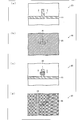
- (A)-(e) is a figure for demonstrating the process of the wiring formation method concerning one embodiment of this invention.
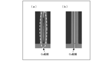
- (A) is a schematic diagram which shows an example of the structure of Cu wiring formed by the conventional wiring formation method
- (b) is an example of the structure of Cu wiring formed by the wiring formation method of this Embodiment.
- (A)-(e) is a figure for demonstrating the other example of the wiring formation method of this invention.
- (A)-(d) is a top view for demonstrating the process of the manufacturing method of the semiconductor substrate concerning one embodiment of this invention.
- FIG. This corresponds to (a) to (d), respectively.
- FIG. This corresponds to (a) to (d), respectively.
- (A)-(d) is a top view for demonstrating the process of the manufacturing method of the semiconductor substrate concerning one embodiment of this invention. This figure shows a step subsequent to the step shown in FIG. (A)-(d) is sectional drawing for demonstrating the process of the manufacturing method of the semiconductor substrate concerning one embodiment of this invention, (a)-(d) of this figure is FIG. This corresponds to (a) to (d), respectively.
- (A) * (b) is a figure for demonstrating the formation method of the conventional Cu wiring.
- FIGS. 1A to 1E to 8A to 8D An embodiment of the present invention is described below with reference to FIGS. 1A to 1E to 8A to 8D. Note that the present embodiment is not limited to this.
- a method for forming a wiring on a substrate using a copper thin film (Cu thin film) as a material will be described.
- a method for manufacturing a semiconductor substrate including a Cu wiring as a metal wiring by applying this Cu wiring forming method will be described.
- FIGS. 1A to 1E are views for explaining a method of forming a Cu wiring in the present embodiment.
- the state in which Cu wiring is formed on a substrate by the formation method of the present embodiment is shown in cross-sectional configuration in order of steps.
- a Cu thin film 12 is formed as a main conductive film on a glass substrate 11 (substrate) by sputtering.
- the thickness of the Cu thin film 12 can be set to, for example, 300 to 400 nm.
- an insulating film 131 used for the liner film 13 is formed on the Cu thin film 12 by a CVD (Chemical Vapor Deposition) method.
- the liner film 13 may be a metal film containing no Cu other than the insulating film.
- the material of the insulating film 131 for example, SiN (silicon nitride) or SiON (silicon oxynitride) can be used.
- the metal film 13 when the liner film 13 is a metal film, the metal film may be formed by sputtering, for example.
- the material of the metal film include Mo (molybdenum), W (tungsten), Cr (chromium), MoN (molybdenum nitride), TiN (titanium nitride), WN (tungsten nitride), and the like.
- the insulating film 131 can have a laminated structure of SiON and a PSG (phosphorus doped glass) film.
- the thickness of the insulating film 131 can be set to 20 to 50 nm, for example.
- a barrier film (lower barrier film) made of Ti or the like is formed by sputtering to a thickness of, for example, 20 to 30 nm below the main conductive film, and the main conductive film is formed thereon.
- a Cu thin film may be laminated.
- the barrier film made of Ti or the like may be patterned by etching simultaneously with etching of the Cu thin film, or may be etched by dry etching depending on the barrier film.
- dry etching for example, a chlorine-based gas is used and the pressure is set to several Torr to several tens Torr.
- a photoresist 14 having a thickness of 2.0 ⁇ m is applied to the upper layer of the insulating film 131, and the photoresist is patterned into a predetermined shape by photolithography.
- Isotropic dry etching such as plasma etching (hereinafter referred to as “dry etching A”) indicated by a solid arrow A is performed to remove a portion of the insulating film 131 exposed from the photoresist 14.
- the photoresist 14 serves as an etching mask.
- the insulating film 131 removed here is indicated by a broken line in FIG.
- the isotropic dry etching A described above may be, for example, RIE or high-density plasma etching in addition to plasma etching.
- the liner film 13 made of the insulating film 131 that remains without being removed is formed only in the lower layer portion of the photoresist 14.
- the photoresist 14 on the liner film 13 made of the insulating film 131 has a shape in which the end portion protrudes like a bowl.
- FIG. 1C the photoresist 14 is removed using a stripping solution (for example, an organic solvent), and the liner film 13 is used as an etching mask, so that FIGS. d) Isotropic wet etching (hereinafter referred to as “wet etching B”) indicated by a broken-line arrow B in FIG. 8 is performed to partially remove the Cu thin film 12 (Cu conductive film) as the main conductive film. .
- a stripping solution for example, an organic solvent
- a specific method of the isotropic wet etching B here is, for example, a spray (shower) at a temperature of 20 to 40 ° C. using a mixed chemical solution such as H 2 O 2 , H 2 SO 4 , and HNO 3.
- a mixed chemical solution such as H 2 O 2 , H 2 SO 4 , and HNO 3.
- the liner film 13 made of the insulating film 131 made of SiN or the like is not removed, and only the Cu thin film 12 is isotropically etched.
- the isotropic wet etching B performed here is, for example, (I) capable of processing a large number of substrates at a time, (II) the cost of equipment and chemicals is low, compared with dry etching such as RIE, for example. III) There are advantages such as a wide selection of etching masks and less damage to the substrate to be etched.
- the liner film 13 on the Cu wiring 12a has a shape in which the end 13b protrudes like a bowl.
- Ar sputter etching sputter etching using Ar ions
- the specific method of Ar sputter etching here is, for example, applying a high DC voltage between the electrodes facing the substrate while introducing Ar gas in a vacuum, and using Ar + ions obtained by ionizing Ar gas. And a sputter etching is performed by applying a bias voltage to the substrate side.
- the Cu wiring 12a can be formed on the glass substrate 11 by the process as described above.
- the insulating film 131 for example, SiN film
- the photosensitive photoresist 14 is applied and patterned thereon.
- adhesion between the Cu thin film 12 to be processed and the photoresist 14 is improved.
- the insulating film 131 that is, the liner film 13
- the photoresist 14 are laminated with higher adhesion.
- the adhesion between the resist such as the photoresist 14 and the adhesion target of the resist is greatly influenced by the state of the outermost surface of the portion to which the resist is applied.
- the liner film 13 is superior to the Cu thin film 12 in terms of surface stability (particularly oxidation).
- FIG. 2B shows an example of the structure of the Cu wiring formed by the method of the present embodiment.
- FIG. 2A shows an example of a structure of a Cu wiring obtained by a conventional wiring forming method (a method of forming a photoresist directly on a Cu thin film).
- the adhesion between the photoresist and the Cu thin film is improved by sandwiching an insulating film (liner film) between the photoresist and the Cu thin film.
- an insulating film liner film
- a method for forming a Cu wiring on a glass substrate is shown, but this is an example, and the present embodiment is not limited to this. That is, there is no particular limitation on the substrate that is the base of the Cu wiring.
- the above method can also be applied when an insulating film or the like is formed on a glass substrate and a Cu wiring is formed on the insulating film.
- 3A to 3E show another example of the Cu wiring forming method of the present embodiment.
- the Cu wiring forming method shown in FIGS. 3A to 3E is applied to simplify the process.
- the liner film 13 made of the insulating film 131 is formed, with the hook-shaped end portion 13b remaining on the Cu wiring 12a.
- the liner film 13 formed on the Cu wiring 12a removes the end portion 13b of the liner film 13 protruding in a bowl shape on the Cu wiring 12a as described above.
- an insulating film that covers the Cu wiring 12a for example, a gate insulating film (GI) shown in FIGS. 6A to 6D described later, or FIG. It can be used as it is as a part of the inorganic interlayer insulating film 32 shown in FIG.
- GI gate insulating film
- the liner film 13 when the liner film 13 is a metal film, it can be used as it is as a part of the wiring by removing the end portion 13b of the liner film 13 protruding in a bowl shape on the Cu wiring 12a as described above. . That is, for example, it can be used as it is as an upper layer wiring of a two-layer wiring having the Cu wiring 12a as a lower layer wiring.
- the entire liner film 13 may be removed instead of removing the end portion 13b of the liner film 13 protruding in a bowl shape on the Cu wiring 12a.
- TFT substrate ⁇ Configuration of semiconductor substrate (TFT substrate) including Cu wiring>
- a method for manufacturing a semiconductor substrate including a Cu wiring by applying the above-described Cu wiring forming method will be described.
- a TFT substrate (active matrix substrate) of an active matrix liquid crystal display device will be described as an example.
- FIG. 4 shows a partial configuration of a TFT substrate formed by the manufacturing method of the present embodiment.
- FIG. 4 shows one of the TFTs 31 constituting the TFT substrate 20.
- a base coat film 22 is formed on the glass substrate 11, and a gate electrode layer 23 is formed in a predetermined shape on the base coat film 22.
- the gate electrode layer 23 constitutes a gate electrode of the TFT 31 and constitutes a scanning signal wiring and the like.
- a gate insulating film 24 is formed on the gate electrode layer 23.
- a semiconductor layer 25 is formed in a predetermined shape on the gate insulating film 24.
- a source electrode layer 29 is formed on the semiconductor layer 25.
- the source electrode layer 29 is patterned into a predetermined shape to constitute a source electrode 26, a drain electrode 27, and the like. Although not shown, the source electrode layer 29 also constitutes a data signal wiring connected to the source electrode 26.
- the TFT 31 is constituted by the gate electrode, the source electrode 26 and the drain electrode 27 with the semiconductor layer 25 interposed therebetween.
- Cu is contained in the conductive film constituting each electrode and wiring.
- FIG. 7 (a) to (d) show the manufacturing process of the TFT substrate 20 in the order of steps.
- FIG. 5 (a) to (d) and FIG. 7 (a) to (d) show the planar configuration of the TFT substrate 20 that changes depending on each process.
- FIGS. 8 (a) to (d) correspond to (a) to (d) in FIG. 5 and (a) to (d) in FIG.
- the cross-sectional structure of the TFT substrate 20 that changes depending on the process is shown.
- FIG. 6 (a) to (d) and FIG. 8 (a) to (d) are the same as the TFT substrate 20 of FIGS. 5 (a) to (d) and FIG. 7 (a) to (d).
- the cross-sectional structure of the XX line part of each is shown.
- a base coat film 22 (not shown) is formed on the glass substrate 21 by sputtering, for example, to a thickness of 10 to 50 nm, and the upper layer thereof is formed. Then, a gate electrode layer 23 is formed.
- the gate electrode layer 23 is formed by laminating a Cu conductive film 23a (Cu layer) on a Ti conductive film 23b (Ti layer).
- the thickness of the Ti conductive film 23b is, for example, 10 to 100 nm
- the thickness of the Cu conductive film 23a is, for example, 200 to 500 nm.
- the base coat film 22 is not necessarily provided.
- the Cu conductive film 23a is formed in a predetermined shape in the same manner as the Cu thin film 12 which is the Cu conductive film by the same processes as shown in FIGS.
- the gate electrode layer 23 is formed by patterning.
- a photoresist (not shown) is formed in a predetermined shape, and isotropic
- the insulating film is patterned into a predetermined shape by performing dry etching.
- the photoresist is removed, and isotropic wet etching is performed using a patterned liner film (not shown) made of the insulating film as an etching mask, so that the Cu conductive film 23a as the main conductive film is partially formed. To remove.
- the liner film, the insulating film, and the photoresist correspond to the liner film 13, the insulating film 131, and the photoresist 14 shown in FIGS. 1A to 1E, respectively.
- the Ti conductive film 23b provided in the lower layer of the Cu conductive film 23a can be simultaneously etched and patterned when the Cu conductive film 23a is etched.
- the gate electrode layer 23 constituting the gate electrode and the scanning signal line is formed.
- the Cu wiring 12a is simplified in FIGS. 1E and 3E. Therefore, the Cu wiring 12a shown in FIGS. 1E and 3E and the gate electrode layer 23 (particularly the Cu conductive film 23a) shown in FIG. 8A have different cross-sectional shapes. However, this difference in cross-sectional shape does not affect the effect of the above-described wiring forming method.
- the shape of the Cu wiring (Cu conductive film) can be patterned into an arbitrary shape depending on the type of liner film and the etching direction.
- a gate insulating film (GI) 24 is deposited by a CVD method so as to cover the gate electrode layer 23.
- the thickness of the gate insulating film 24 is, for example, 200 to 500 nm.
- a semiconductor layer 25 is deposited by a CVD method.
- the semiconductor layer 25 includes an amorphous silicon film (a-Si layer) 25a not doped with impurities and an n + amorphous silicon film (n + layer) 25b doped with impurities.
- a-Si layer amorphous silicon film
- n + layer amorphous silicon film
- the thickness of the amorphous silicon film (a-Si layer) 25a is, for example, 50 to 200 nm
- the thickness of the n + amorphous silicon film (n + layer) 25b is, for example, 10 to 70 nm.
- the photoresist 41 is patterned into a predetermined shape by photolithography. Then, dry etching is performed to remove the semiconductor layer 25 that is not covered with the photoresist 41, and the gate insulating film 24 is exposed.
- etching general dry etching using a fluorine-based or chlorine-based gas is employed.
- a fluorine-based gas such as CF 4 , SF 6 , or NF 3
- a chlorine-based gas such as Cl 2 , HCl, or BCl 3 is used.
- the island-shaped semiconductor layer 25 is formed.
- the source electrode layer 29 is sputtered so as to cover the semiconductor layer 25. To form a film.
- the source electrode layer 29 is formed by laminating a Cu conductive film 29a on a Ti conductive film 29b as shown in FIG. 6 (d) and FIG. 8 (a).
- the thickness of the Ti conductive film 29b is, for example, 10 to 100 nm
- the thickness of the Cu conductive film 29a is, for example, 200 to 500 nm.
- the photoresist 42 is patterned into a predetermined shape by lithography.
- the channel portion of the TFT 31 is removed by wet etching and dry etching to form the TFT 31.
- the patterning of the source electrode layer 29 can also be performed according to the above-described Cu wiring formation method (see FIGS. 1A to 1E).
- an insulating film such as SiN used for the liner film is formed on the source electrode layer 29.
- the insulating film is patterned into a predetermined shape by photolithography.
- the photoresist 42 is removed, and isotropic wet etching is performed using the patterned liner film made of the insulating film as an etching mask to partially remove the Cu conductive film 29a.
- the source electrode 26, the drain electrode 27, and the data signal wiring including the Cu conductive film 29a are patterned into a predetermined shape.
- the liner film, the insulating film, and the photoresist correspond to the liner film 13, the insulating film 131, and the photoresist 14 shown in FIGS. 1A to 1E, respectively.
- the Ti conductive film 29b provided in the lower layer of the Cu conductive film 29a may be patterned by etching simultaneously when etching the Cu conductive film 29a, or at the time of etching the semiconductor layer 25 performed later. Etching may be performed.
- the patterning method of the Ti conductive film 29b can be appropriately selected depending on the material of the insulating film (liner film) formed on the Cu conductive film 29a.
- the n + amorphous silicon film 25b in the semiconductor layer 25 is removed by dry etching to form a channel region in which the amorphous silicon film (a-Si layer) 25a is exposed.
- the etching of the semiconductor layer 25 is performed using chlorine-based gas or fluorine-based gas under a pressure of several torr to several tens of Torr.
- the TFT 31 portion is completed as shown in FIGS. 7B and 8B.
- the inorganic interlayer insulating film 32 (Pas, see FIG. 8C) and the organic interlayer insulating film 33 (JAS) are formed by CVD. Is used to form a film on the entire TFT substrate 20.
- the thickness of the inorganic interlayer insulating film 32 formed here is, for example, 70 to 300 nm, and the thickness of the organic interlayer insulating film 33 is, for example, 500 to 3000 nm.
- a transparent conductive layer 34 such as ITO (or IZO) is formed as a film for forming the pixel electrode. Then, by performing photolithography, a pixel electrode patterned into a predetermined shape is formed.
- the pixel electrode (ITO) 34 is electrically connected to the drain electrode 27 through a contact hole formed in the inorganic interlayer insulating film 32 and the organic interlayer insulating film 33.
- the method for manufacturing a semiconductor substrate according to the present embodiment patterns the gate electrode layer and the source electrode layer formed on the semiconductor substrate using the above-described method for forming a metal wiring containing Cu.
- the semiconductor element such as TFT and the wiring are patterned.
- the wiring forming method includes a step of forming a metal thin film containing Cu on a substrate, and a metal film containing no insulating film or Cu on the metal thin film (that is, ( 1) an insulating film and (2) a film selected from the group consisting of a metal film containing no Cu), and photolithography on the insulating film or the metal film containing no Cu
- a step of patterning a photoresist by using isotropic dry etching a step of etching the insulating film or a metal film not containing Cu using the photoresist as an etching mask, and a step of etching the insulating film or Cu.
- the photoresist After etching the metal film not containing the photoresist, the photoresist is removed, and the isotropic wet etch is performed using the metal film not containing the insulating film or Cu as an etching mask. Perform ring, the metal thin film is partially removed, and a step for forming a metal wiring, a.
- the semiconductor element and the wiring are formed by patterning the gate electrode layer and the source electrode layer containing Cu using the wiring forming method described above.
- the insulating film is preferably made of SiN or SiON.
- the adhesion between the photoresist and the insulating film can be further increased by using SiN or SiON as the material of the insulating film.
- the metal film not containing Cu is preferably made of any one of molybdenum, tungsten, chromium, molybdenum nitride, titanium nitride, and tungsten nitride.
- the metal film that does not contain Cu is any one of molybdenum, tungsten, chromium, molybdenum nitride, titanium nitride, and tungsten nitride, so that the metal that does not contain photoresist and Cu.
- the adhesion strength with the film can be further increased.
- the wiring forming method further includes a step of removing an end portion of the insulating film or the metal film not containing Cu on the metal wiring containing Cu by sputter etching.
- the end portion of the insulating film protruding from the metal wiring or the metal film not containing Cu can be removed.
- Ar ions are preferably used for the sputter etching.
- the metal thin film containing Cu may have a laminated structure of a Ti layer and a Cu layer.
- the semiconductor element is, for example, a TFT, an LSI, a thin film solar cell element, a micromachine, or the like.
- the semiconductor substrate for example, an active matrix substrate can be cited.
- Cu wiring can be formed with a wiring width and wiring height as designed. Therefore, the method of the present invention can be applied to the manufacture of a semiconductor substrate included in a display device or the like.
Landscapes
- Internal Circuitry In Semiconductor Integrated Circuit Devices (AREA)
- Thin Film Transistor (AREA)
Abstract
本発明の配線形成方法は、基材としてのガラス基板(11)上にCuを含む金属薄膜(12)を成膜する工程と、金属薄膜(12)上に、絶縁膜またはCuを含まない金属膜である絶縁膜(131)を形成する工程と、絶縁膜(131)上に、フォトリソグラフィーを用いてフォトレジスト(14)をパターニングする工程と、等方性のドライエッチングを用いて、フォトレジスト(14)をエッチングマスクとしてライナー膜(13)をエッチングする工程と、ライナー膜(13)のエッチング後、フォトレジスト(14)を除去し、ライナー膜(13)をエッチングマスクとして等方性のウエットエッチングを行い、金属薄膜(12)を部分的に除去し、金属配線(12a)を形成する工程と、を含む。
Description
本発明は、基板上にCu配線を形成する方法、および、Cu配線を含む半導体基板の製造方法に関する。
半導体デバイスを高集積化するために配線を微細化し、また、半導体デバイスの動作速度を高速化するために配線電流密度を増大させると、エレクトロマイグレーションによる配線の信頼性低下が問題となる。
現在、半導体デバイスに広く用いられているAl配線は、エレクトロマイグレーション耐性に劣るため、これに代わる種々の配線材料が検討されている。CuはAlに代わる配線材料のひとつとして注目されている。
Cu配線形成の方法としては、基板上に形成したCu薄膜上に、レジストとしてフォトレジストを形成した後、フォトリソグラフィーにてパターニングし、等方性エッチングであるウエットエッチングを行う方法が挙げられる。
しかしながら、この方法では、図2の(a)に示すように、配線の一部に、配線幅が細くなったり、配線高さが低くなる箇所が存在し、断線が生じたり抵抗が増大したりしてしまうという問題が発生する。
これは、Cu薄膜の表面は、比較的低温で酸化等の表面反応を起こしやすく、その状態が不安定なことが原因であり、Cu薄膜の表面状態によってはフォトレジストとの密着力が極めて低下する場合がある。
フォトレジストとCu薄膜表面との密着力が弱いと、Cu薄膜上にフォトレジストを形成してパターニングする際に、局所的にレジストが浮き上がってしまい、上記のような問題が発生する。
このように、レジストがCu薄膜表面に密着されていないと、設計通りの寸法(配線幅および配線高さ)で配線を形成することができない。
また、特許文献1には、異方性エッチングであるRIE(Reactive Ion Etching;反応性イオンエッチング)法を用いて、Cuを配線形状にエッチング加工するという技術が開示されている。
このCu配線形成技術では、図9の(a)に示すように、下地110上に、TiNバリア層112(下層のバリア層)、Cu層114、及びTiNバリア層116(上層のバリア層)を順次積層した後、上層のバリア層であるTiNバリア層116上にSiO2エッチングマスク118aを形成する。
次に、RIE法により、エッチングマスクを介して上層のTiNバリア層116、Cu層114、及び下層のTiNバリア層112を順次エッチングし、配線形状に加工する。
この際、エッチングガスとして、例えばSiCl4、Cl2、及びN2の混合ガスを用いる。ここで、エッチングガス中のSi及びCl原子個数の比を制御することにより、図9の(b)に示すように、上層のTiNバリア層116、Cu層114、及び下層のバリア層112をエッチングしながら、これらのエッチング加工側壁面に側壁バリア層122としてSiOXNYバリア層を堆積させる。
このように、特許文献1のCu配線形成技術では、Cu層をエッチング加工するときに、エッチングマスクと反応性エッチングガスとの間で反応生成物を生じさせ、この反応生成物を、Cu層のエッチング加工側壁面114lに堆積させることにより、側壁バリア層122を形成している。
したがって、エッチングと同時に側壁バリア層122を形成できるため、側壁バリア層122の形成のための熱処理を省くことができる。このため、側壁バリア層122の形成を、半導体素子の劣化を招かないような低温で行うことができる。
上記特許文献1に記載の技術のように、RIE法を用いて異方性のドライエッチングを行えば、ウエットエッチングによって配線のパターニングを行う方法と比較して、より微細な加工を行うことができる。
しかしながら、RIE法では真空チャンバー(図9の(a)・(b)に示す反応室123)などの特殊な装置が必要となり、製造コストが増大してしまうという問題点がある。
また、Cuは反応蒸気圧が低いために反応速度が極端に遅く、RIE法によるドライエッチングでは処理速度が極めて遅なってしまい、生産性が低下するという問題もある。
本発明は、上記の問題点に鑑みてなされたものであり、ウエットエッチングを用いて設計どおりの寸法でCu配線を形成する方法を提供することを目的とする。
上記の課題を解決するために、配線形成方法は、基材上にCuを含む金属薄膜を成膜する工程と、上記金属薄膜上に絶縁膜またはCuを含まない金属膜(すなわち、(1)絶縁膜、および、(2)Cuを含まない金属膜、からなる群より選ばれる何れか一方の膜)を形成する工程と、上記絶縁膜またはCuを含まない金属膜上に、フォトリソグラフィーを用いてフォトレジストをパターニングする工程と、等方性のドライエッチングを用いて、上記フォトレジストをエッチングマスクとして上記絶縁膜またはCuを含まない金属膜をエッチングする工程と、上記絶縁膜またはCuを含まない金属膜のエッチング後、上記フォトレジストを除去し、上記絶縁膜またはCuを含まない金属膜をエッチングマスクとして等方性のウエットエッチングを行い、上記金属薄膜を部分的に除去し、金属配線を形成する工程と、を含んでいる。
上記の方法においては、Cuを含む金属薄膜とフォトレジストとの間に、エッチング選択性を有するライナー膜として、上記したように絶縁膜またはCuを含まない金属膜を形成している。
絶縁膜またはCuを含まない金属膜の表面状態は、Cuの表面状態と比較して酸化等の反応を起こしにくく安定している。そのため、Cuを含む金属薄膜とフォトレジストとの密着力と比較して、絶縁膜(またはCuを含まない金属膜)とフォトレジストとの密着力は強い。したがって、上記金属薄膜上に絶縁膜またはCuを含まない金属膜を形成し、その上層にフォトレジストを形成すれば、フォトレジストが浮き上がってしまうことがなくなる。
したがって、上記の方法によれば、フォトレジストと金属薄膜との間に絶縁膜またはCuを含まない金属膜を挟むことで、フォトレジストと加工対象となる金属薄膜との密着性が向上し、配線加工の際の局部的な配線パターンの崩れを抑制することができ、配線抵抗の増大、および、断線を招来する配線の欠陥などを無くすことが可能となるという効果が得られる。
また、上記の方法によれば、金属配線の形成を行う場合に、より簡便な設備および工程で処理が可能なウエットエッチングを用いても、設計どおりの寸法でCuを材料とする金属配線を形成することができる。また、Cuを含む金属薄膜は、RIE法によるドライエッチングで加工を行うと、処理速度が極めて遅なってしまうという問題もあるが、上記の方法では、本発明ではウエットエッチングを行うため、適度な処理速度で加工を行うことができ、高い生産性を保つことができる。
上記の課題を解決するために、半導体基板の製造方法では、上記の配線形成方法を用いて、Cuを含むゲート電極層およびソース電極層をパターニングして半導体素子および配線を形成する。
上記の製造方法によれば、配線材料としてCu導電膜を使用した場合に、設計どおりの配線幅および配線高さで配線を形成することができるという効果が得られる。
上記したように、配線形成方法は、基材上にCuを含む金属薄膜を成膜する工程と、上記金属薄膜上に絶縁膜またはCuを含まない金属膜を形成する工程と、上記絶縁膜またはCuを含まない金属膜上に、フォトリソグラフィーを用いてフォトレジストをパターニングする工程と、等方性のドライエッチングを用いて、上記フォトレジストをエッチングマスクとして上記絶縁膜またはCuを含まない金属膜をエッチングする工程と、上記絶縁膜またはCuを含まない金属膜のエッチング後、上記フォトレジストを除去し、上記絶縁膜またはCuを含まない金属膜をエッチングマスクとして等方性のウエットエッチングを行い、上記金属薄膜を部分的に除去し、金属配線を形成する工程と、を含んでいる。
上記の方法によれば、金属配線の形成を行う場合に、より簡便な設備および工程で処理が可能なウエットエッチングを用いても、設計どおりの寸法でCuを材料とする金属配線を形成することができるという効果を奏する。
本発明の一実施形態について図1の(a)~(e)ないし図8の(a)~(d)に基づいて説明すると以下の通りである。なお、本実施の形態はこれに限定されるものではない。
本実施の形態では、まず、基板上に銅薄膜(Cu薄膜)を材料として配線を形成する方法について説明する。続いて、このCu配線の形成方法を応用して、Cu配線を金属配線として含む半導体基板を製造する方法について説明する。
<Cu配線の形成方法>
図1の(a)~(e)は、本実施の形態におけるCu配線の形成方法を説明するための図である。図1の(a)~(e)では、本実施の形態の形成方法によって、基板上にCu配線が形成される様子を、工程順に、その断面構成で示している。
図1の(a)~(e)は、本実施の形態におけるCu配線の形成方法を説明するための図である。図1の(a)~(e)では、本実施の形態の形成方法によって、基板上にCu配線が形成される様子を、工程順に、その断面構成で示している。
図1の(a)に示すように、まず、ガラス基板11(基板)上に、主導電膜としてCu薄膜12をスパッタリングにより成膜する。ここでのCu薄膜12の厚さは、例えば、300~400nmとすることができる。
その後、Cu薄膜12上に、ライナー膜13(図1の(b)参照)に用いられる絶縁膜131をCVD(Chemical Vapor Deposition;化学蒸着)法によって形成する。なお、ライナー膜13としては、絶縁膜以外に、Cuを含まない金属膜であってもよい。
上記絶縁膜131の材料としては、例えば、SiN(窒化ケイ素)、SiON(酸窒化ケイ素)を用いることができる。
また、ライナー膜13が金属膜である場合には、金属膜を例えばスパッタリングにて形成してもよい。上記金属膜の材料としては例えば、Mo(モリブデン)、W(タングステン)、Cr(クロム)、MoN(窒化モリブデン)、TiN(窒化チタン)、WN(窒化タングステン)などが挙げられる。
また、絶縁膜131は、SiONとPSG(リンドープガラス)膜などとの積層構造とすることもできる。絶縁膜131の厚さは、例えば、20~50nmとすることができる。
なお、図示はしていないが、主導電膜の下層にTiなどからなるバリア膜(下層バリア膜)を、スパッタリングにより、例えば厚さ20~30nmで成膜し、その上層に主導電膜であるCu薄膜を積層してもよい。
このTiなどからなるバリア膜は、Cu薄膜をエッチングする際に、同時にエッチング加工してパターニングしてもよいし、バリア膜によっては、ドライエッチングによりエッチング加工してもよい。ドライエッチングでは、例えば、塩素系ガスを用い、圧力は数Torr~数十Torrで行う。
次に、絶縁膜131の上層に膜厚2.0μmのフォトレジスト14を塗布し、フォトリソグラフィーによって該フォトレジストを所定形状にパターニングする。
その後、例えば、CF4およびC2F6の混合ガス、または、CF4またはC2F6の混合ガスにO2を添加したものを用いて、図1の(a)・(b)中に実線の矢印Aで示す、プラズマエッチングなどの等方性のドライエッチング(以下、「ドライエッチングA」と記す)を行い、上記絶縁膜131のうち、フォトレジスト14から露出した部分を除去する。
ここでの等方性のドライエッチングAでは、フォトレジスト14がエッチングマスクとなる。ここで除去される絶縁膜131は、図1の(a)において破線で示す。
なお、上記の等方性のドライエッチングAは、プラズマエッチング以外に、例えば、RIE、または高密度プラズマエッチング等であってもよい。
これにより、図1の(b)に示すように、フォトレジスト14の下層の部分のみに、除去されずに残った絶縁膜131からなるライナー膜13が形成される。
なお、等方性のドライエッチングAを行うことで、絶縁膜131においてフォトレジスト14に被覆されている領域であっても、フォトレジスト14の端部近傍では、エッチング処理され除去される。つまり、図1の(b)に示すように、上記絶縁膜131からなるライナー膜13上のフォトレジスト14は、その端部が庇状に突出した形状となる。
続いて、図1の(c)に示すように、フォトレジスト14を剥離液(例えば、有機溶剤)などを用いて除去し、ライナー膜13をエッチングマスクにして、図1の(c)・(d)中に破線の矢印Bで示す、等方性のウエットエッチング(以下、「ウエットエッチングB」と記す)を行い、主導電膜であるCu薄膜12(Cu導電膜)を部分的に除去する。
ここでの等方性のウエットエッチングBの具体的な方法は、例えば、H2O2、H2SO4、HNO3等の混合薬液を用い、20~40℃の温度で、スプレー(シャワー)にて基板に対して上記混合薬液を噴出し、エッチング加工を行うというものである。
この条件で等方性のウエットエッチングBを行うことによって、SiNなどで形成された、絶縁膜131からなるライナー膜13は除去されず、Cu薄膜12のみが等方的にエッチング処理される。
ここで行う等方性のウエットエッチングBは、例えばRIE法などのドライエッチングと比較して、例えば、(I)一度に大量の基板を処理できる、(II)装置や薬品の価格が安い、(III)エッチングマスクの選択の幅が広くエッチングされる基材に与える損傷が少ない、などの利点がある。
これにより、図1の(d)に示すように、Cu薄膜12が所定形状にパターニングされたCu配線12aが得られる。
図1の(d)では、等方性のウエットエッチングBによって除去されるCu薄膜12を破線で示す。
なお、等方性のウエットエッチングBを行うことで、Cu薄膜12においてライナー膜13に被覆されている領域であっても、ライナー膜13の端部近傍では、エッチング処理され除去される。つまり、図1の(d)に示すように、Cu配線12a上のライナー膜13は、その端部13bが庇状に突出した形状となる。
その後、図1の(e)に一点鎖線の矢印Cで示すように、Arイオンを用いたスパッタエッチング(以下、「Arスパッタエッチング」と記す)を行い、Cu配線12a上において庇状に突出したライナー膜13の端部13bを除去する。
なお、ここでのArスパッタエッチングの具体的な方法は、例えば、真空中にArガスを導入しながら基板と対向する電極間に直流高電圧を印加して、Arガスをイオン化したAr+イオンを生成し、基板側にバイアス電圧を印加してスパッタエッチングを行うというものが挙げられる。
上記のような工程により、ガラス基板11上にCu配線12aを形成することができる。
<上記のCu配線の形成方法による効果>
上記のCu配線の形成方法によれば、Cu薄膜12上に、ライナー膜13となる絶縁膜131(例えば、SiN膜)を積層し、その上に感光性のフォトレジスト14を塗布しパターニングすることで、加工対象のCu薄膜12とフォトレジスト14との密着性(ライナー膜13を介しての間接的な接着性)が向上する。
上記のCu配線の形成方法によれば、Cu薄膜12上に、ライナー膜13となる絶縁膜131(例えば、SiN膜)を積層し、その上に感光性のフォトレジスト14を塗布しパターニングすることで、加工対象のCu薄膜12とフォトレジスト14との密着性(ライナー膜13を介しての間接的な接着性)が向上する。
より具体的には、Cu薄膜12と比較して表面状態の安定した絶縁膜131(すなわち、ライナー膜13)とフォトレジスト14とがより高い密着力で積層される。
これにより、配線加工の際の局部的な配線パターンの崩れを抑制することができ、配線抵抗の増大、および、断線を引き起こす配線の欠陥などを無くすことが可能となるという効果が得られる。
このように、フォトレジスト14などのレジストと、該レジストの密着対象との密着性は、レジストが塗布される部分の最表面の状態に大きく影響される。表面の安定性(特に酸化性)は、Cu薄膜12よりもライナー膜13のほうが優れている。
図2の(b)には、本実施の形態の方法によって形成されたCu配線の構造の一例を示す。また、比較のために、図2の(a)には、従来の配線形成方法(Cu薄膜上に直接フォトレジストを形成する方法)によって得られたCu配線の構造の一例を示す。
従来の方法によってCu配線を形成すると、フォトレジストとCu薄膜表面との間の密着力が乏しいために、局所的にフォトレジストが浮き上がってしまい、設計どおりの配線幅および配線高さで配線形成を行うことができなかった。そのため、図2の(a)に示すように、配線パターンが崩れてしまうという問題が生じていた。
これに対して、本実施の形態の方法によってCu配線を形成すると、フォトレジストとCu薄膜との間に絶縁膜(ライナー膜)を挟むことで、フォトレジストとCu薄膜との密着性が向上し、配線加工の際の局部的な配線パターンの崩れを抑制することができる。
これにより、図2の(b)に示すように、配線抵抗の増大、および、断線を招来する配線の欠陥などを無くすことが可能となる。
なお、ここでは、ガラス基板上にCu配線を形成する方法について示しているが、これは一例であり、本実施の形態はこれに限定はされない。つまり、Cu配線の土台となる基板については、特に限定はされない。また、ガラス基板上に、絶縁膜などを形成し、該絶縁膜上にCu配線を形成する場合にも、上記方法を適用することができる。
<Cu配線の形成方法の変形例>
また、図3の(a)~(e)には、本実施の形態のCu配線の形成方法の他の例を示す。
また、図3の(a)~(e)には、本実施の形態のCu配線の形成方法の他の例を示す。
図3に示すCu配線の形成方法では、図1の(e)に示す、Cu配線12a上において庇状に突出したライナー膜13の端部13bを、Arスパッタエッチングにより除去する工程が省略されている。
それ以外の工程(すなわち、図3の(a)~(d)に示す各工程)は、図1の(a)~(d)に示す各工程と同じである。
目的とする半導体デバイスにおいて、庇状のライナー膜13の端部13bの存在が品質上問題なければ、図3の(a)~(e)に示すCu配線の形成方法を適用し、工程を簡略化することができる。
この配線形成方法によれば、図3の(e)に示すように、Cu配線12a上に庇状の端部13bが残存した、絶縁膜131からなるライナー膜13が形成される。
なお、上記した各配線形成方法において、Cu配線12a上に形成されたライナー膜13は、上記したようにCu配線12a上において庇状に突出したライナー膜13の端部13bを除去することで、ライナー膜13が絶縁膜である場合、Cu配線12aを覆う絶縁膜(例えば、後述する図6の(a)~(d)に示すゲート絶縁膜(GI)、あるいは、図8の(c)・(d)に示す無機層間絶縁膜32など)の一部としてそのまま利用することができる。
また、ライナー膜13が金属膜である場合、上記したようにCu配線12a上において庇状に突出したライナー膜13の端部13bを除去することで、配線の一部としてそのまま利用することができる。すなわち、例えば、Cu配線12aを下層配線とする二層配線の上層配線としてそのまま利用することができる。
なお、勿論、Cu配線12a上において庇状に突出したライナー膜13の端部13bを除去する代わりに、ライナー膜13全体を除去してもよい。
<Cu配線を含む半導体基板(TFT基板)の構成>
続いて、上記のCu配線の形成方法を応用して、Cu配線を含む半導体基板を製造する方法について説明する。以下では、半導体基板の一例として、アクティブマトリクス型の液晶表示装置のTFT基板(アクティブマトリクス基板)を例に挙げて説明する。
続いて、上記のCu配線の形成方法を応用して、Cu配線を含む半導体基板を製造する方法について説明する。以下では、半導体基板の一例として、アクティブマトリクス型の液晶表示装置のTFT基板(アクティブマトリクス基板)を例に挙げて説明する。
そこで、まず、図4を参照して、上記TFT基板の構成について説明する。
図4には、本実施の形態の製造方法によって形成されるTFT基板の部分構成を示す。なお、図4では、TFT基板20を構成しているTFT31の一つを示す。
図4に示すように、TFT基板20では、ガラス基板11上にベースコート膜22が成膜されており、その上層にゲート電極層23が所定形状に形成されている。ゲート電極層23は、TFT31のゲート電極を構成するとともに走査信号配線などを構成する。ゲート電極層23の上層には、ゲート絶縁膜24が形成されている。
ゲート絶縁膜24上には、半導体層25が所定形状に形成されている。そして、半導体層25の上層には、ソース電極層29が形成されている。
ソース電極層29は、所定形状にパターニングされて、ソース電極26およびドレイン電極27などを構成する。また、図示はしていないが、ソース電極層29は、ソース電極26に接続されるデータ信号配線も構成する。
半導体層25を間に挟んで、ゲート電極、ソース電極26およびドレイン電極27によって、TFT31が構成される。
なお、上記のTFT基板20では、各電極および配線を構成している導電膜にCuが含まれている。
<上記TFT基板の製造方法>
次に、上記のような構成を有するTFT基板20の製造方法を、図5の(a)~(d)ないし図8の(a)~(d)を参照しながら以下に説明する。
次に、上記のような構成を有するTFT基板20の製造方法を、図5の(a)~(d)ないし図8の(a)~(d)を参照しながら以下に説明する。
図5の(a)~(d)および図7の(a)~(d)には、TFT基板20の製造工程を工程順に示す。
図5の(a)~(d)および図7の(a)~(d)では、各工程によって変化するTFT基板20の平面構成を示す。
また、図6の(a)~(d)および図8の(a)~(d)は、図5の(a)~(d)および図7の(a)~(d)に対応する各工程によって変化するTFT基板20の断面構成を示す。
なお、図6の(a)~(d)および図8の(a)~(d)は、図5の(a)~(d)および図7の(a)~(d)のTFT基板20のX-X線部分の断面構成をそれぞれ示している。
まず、図5の(a)および図6の(a)に示すように、ガラス基板21上にベースコート膜22(図示せず)をスパッタリングにより、例えば厚さ10~50nmで成膜し、その上層にゲート電極層23を成膜する。
ゲート電極層23は、図6の(a)に示すように、Ti導電膜23b(Ti層)上にCu導電膜23a(Cu層)を積層して形成される。
ここで、Ti導電膜23bの厚さは、例えば10~100nmであり、Cu導電膜23aの厚さは、例えば200~500nmである。なお、上記ベースコート膜22は必ずしも設けられていなくてもよい。
そして、上述したCu配線の形成方法にしたがって、図1の(a)~(e)に示す工程と同様の工程により、Cu導電膜であるCu薄膜12と同様にしてCu導電膜23aを所定形状にパターニングして、ゲート電極層23を形成する。
具体的には、Cu導電膜23a上に、ライナー膜に用いられる、SiNなどの絶縁膜(図示せず)を成膜した後、フォトレジスト(図示せず)を所定形状に形成し、等方性のドライエッチングを行うことにより、上記絶縁膜を所定形状にパターニングする。
その後、上記フォトレジストを除去し、パターニングされた上記絶縁膜からなるライナー膜(図示せず)をエッチングマスクにして、等方性のウエットエッチングを行い、主導電膜であるCu導電膜23aを部分的に除去する。
なお、上記ライナー膜、絶縁膜、フォトレジスト、は、それぞれ、図1の(a)~(e)に示すライナー膜13、絶縁膜131、フォトレジスト14に対応する。
なお、Cu導電膜23aの下層に設けられたTi導電膜23bは、Cu導電膜23aをエッチングする際に同時にエッチング加工してパターニングすることができる。
これにより、図5の(a)および図6の(a)に示すように、ゲート電極および走査信号線を構成するゲート電極層23が形成される。
なお、図1の(e)および図3の(e)ではCu配線12aを簡略化して示している。このため、図1の(e)および図3の(e)に示すCu配線12aと、図8の(a)に示すゲート電極層23(特に、Cu導電膜23a)とでは断面形状が異なっているが、この断面形状の違いは、上述した配線形成方法による効果に影響を与えるものではない。
また、Cu配線(Cu導電膜)の形状は、ライナー膜の種類やエッチング方向によって、任意の形状にパターニングすることができる。
次に、図6の(a)に示すように、ゲート電極層23を覆うようにゲート絶縁膜(GI)24をCVD法によって堆積する。ここで、ゲート絶縁膜24の厚さは、例えば200~500nmである。
その後、図5の(a)および図6の(a)に示すように、半導体層25をCVD法によって堆積する。
半導体層25は、不純物がドープされていないアモルファスシリコン膜(a-Si層)25aと、不純物がドープされたn+アモルファスシリコン膜(n+層)25bとから構成されている。
なお、アモルファスシリコン膜(a-Si層)25aの厚さは、例えば50~200nmであり、n+アモルファスシリコン膜(n+層)25bの厚さは、例えば10~70nmである。
ここで、積層された半導体層25を所定形状にパターニングするために、図5の(b)および図6の(b)に示すように、フォトリソグラフィーによってフォトレジスト41を所定形状にパターニングする。そして、ドライエッチングを行い、フォトレジスト41に覆われていない半導体層25を除去し、ゲート絶縁膜24を露出させる。
ここでのエッチングには、フッ素系や塩素系のガスを用いた一般的なドライエッチングを採用する。例えば、Siを含む半導体層のドライエッチングには、CF4、SF6、NF3などのフッ素系のガス、あるいは、Cl2、HCl、BCl3などの塩素系のガスを用いる。
上記の工程により、図5の(c)および図6の(c)に示すように、島状の半導体層25が形成される。
続いて、図5の(d)、図6の(d)、図7の(a)、および図8の(a)に示すように、半導体層25を覆うように、ソース電極層29をスパッタリングによって成膜する。
ソース電極層29は、ゲート電極層23と同様に、図6の(d)および図8の(a)示すように、Ti導電膜29b上にCu導電膜29aを積層して形成される。
ここで、Ti導電膜29bの厚さは、例えば10~100nmであり、Cu導電膜29aの厚さは、例えば200~500nmである。
次に、ソース電極層29を所定形状にパターニングするために、図5の(d)、図6の(d)、図7の(a)、および図8の(a)に示すように、フォトリソグラフィーによってフォトレジスト42を所定形状にパターニングする。
そして、図7の(b)および図8の(b)に示すように、TFT31のチャネル部をウエットエッチングおよびドライエッチングにより、エッチング除去し、TFT31を形成する。
なお、ここでのソース電極層29のパターニングの際にも、上述したCu配線の形成方法(図1の(a)~(e)参照)にしたがって、パターニングを行うことができる。
具体的には、まず、フォトレジスト42を形成する前に、ソース電極層29上に、ライナー膜に用いられる、SiNなどの絶縁膜(図示せず)を成膜する。
そして、上記絶縁膜上に積層されたフォトレジスト42をフォトリソグラフィーによって所定形状にパターニングした後、等方性のドライエッチングを行うことにより、上記絶縁膜を所定形状にパターニングする。
その後、フォトレジスト42を除去し、パターニングされた上記絶縁膜からなるライナー膜をエッチングマスクにして等方性のウエットエッチングを行い、主導電膜であるCu導電膜29aを部分的に除去する。
これにより、Cu導電膜29aを含んでなるソース電極26、ドレイン電極27、および、データ信号配線が、所定形状にパターニングされる。
なお、上記ライナー膜、絶縁膜、フォトレジスト、は、それぞれ、図1の(a)~(e)に示すライナー膜13、絶縁膜131、フォトレジスト14に対応する。
なお、Cu導電膜29aの下層に設けられたTi導電膜29bは、Cu導電膜29aをエッチングする際に、同時にエッチング加工してパターニングしてもよいし、後で行われる半導体層25のエッチング時にエッチング加工してもよい。
このTi導電膜29bのパターニング方法は、Cu導電膜29a上に形成された絶縁膜(ライナー膜)の材料によって適宜選択することができる。
その後、半導体層25のうちのn+アモルファスシリコン膜25bをドライエッチングにより除去し、アモルファスシリコン膜(a-Si層)25aが露出したチャネル領域を形成する。例えば、この半導体層25のエッチングには、塩素系ガスやフッ素系ガスを用い、数Torr~数十Torrの圧力下でエッチングを行う。
以上の工程により、図7の(b)および図8の(b)に示すように、TFT31部分が完成する。
続いて、図7の(c)および図8の(c)に示すように、無機層間絶縁膜32(Pas、図8の(c)参照)および有機層間絶縁膜33(JAS)を、CVD法を用いてTFT基板20全体に成膜する。
ここで形成される無機層間絶縁膜32の厚さは、例えば70~300nmであり、有機層間絶縁膜33の厚さは、例えば500~3000nmである。
その後、図7の(d)および図8の(d)に示すように、画素電極を形成するための膜としてITO(またはIZO)などの透明導電層34を成膜する。そして、フォトリソグラフィーを行うことにより、所定の形状にパターニングされた画素電極が形成される。
なお、図示はしていないが、画素電極(ITO)34は、無機層間絶縁膜32及び有機層間絶縁膜33に形成されたコンタクトホールを介して、ドレイン電極27に電気的に接続されている。
以上のように、本実施の形態にかかる半導体基板の製造方法は、上述したCuを含む金属配線の形成方法を用いて、半導体基板上に形成された、ゲート電極層およびソース電極層をパターニングし、TFTなどの半導体素子および配線をパターニングするというものである。
この方法によれば、配線材料としてCu導電膜を使用した場合に、設計どおりの配線幅および配線高さで配線を形成することができるという効果を得ることができる。
具体的には、本実施の形態にかかる配線形成方法は、基材上にCuを含む金属薄膜を成膜する工程と、上記金属薄膜上に絶縁膜またはCuを含まない金属膜(すなわち、(1)絶縁膜、および、(2)Cuを含まない金属膜、からなる群より選ばれる何れか一方の膜)を形成する工程と、上記絶縁膜またはCuを含まない金属膜上に、フォトリソグラフィーを用いてフォトレジストをパターニングする工程と、等方性のドライエッチングを用いて、上記フォトレジストをエッチングマスクとして上記絶縁膜またはCuを含まない金属膜をエッチングする工程と、上記絶縁膜またはCuを含まない金属膜のエッチング後、上記フォトレジストを除去し、上記絶縁膜またはCuを含まない金属膜をエッチングマスクとして等方性のウエットエッチングを行い、上記金属薄膜を部分的に除去し、金属配線を形成する工程と、を含んでいる。
そして、上記の半導体基板の製造方法では、上記の配線形成方法を用いて、Cuを含むゲート電極層およびソース電極層をパターニングして半導体素子および配線を形成する。
上記の配線形成方法において、上記絶縁膜は、SiNまたはSiONを材料とするものであることが好ましい。
上記の配線形成方法によれば、絶縁膜の材料をSiNまたはSiONとすることで、フォトレジストと絶縁膜との密着力をより高めることができる。
また、上記の配線形成方法において、上記Cuを含まない金属膜は、モリブデン、タングステン、クロム、窒化モリブデン、窒化チタン、および窒化タングステンのうちの何れかを材料とするものであることが好ましい。
上記の配線形成方法によれば、Cuを含まない金属膜の材料をモリブデン、タングステン、クロム、窒化モリブデン、窒化チタン、および窒化タングステンのうちの何れかとすることで、フォトレジストとCuを含まない金属膜との密着力をより高めることができる。
また、上記の配線形成方法は、スパッタエッチングによって、上記Cuを含む金属配線上の上記絶縁膜またはCuを含まない金属膜の端部を除去する工程をさらに含むことが好ましい。
上記の配線形成方法によれば、金属配線から突出した絶縁膜またはCuを含まない金属膜の端部を除去することができる。なお、上記のスパッタエッチングには、Arイオンを用いることが好ましい。
また、上記の配線形成方法において、上記Cuを含む金属薄膜は、Ti層とCu層との積層構造を有していてもよい。
また、上記の半導体基板の製造方法において、半導体素子とは、例えば、TFT、LSI、薄膜太陽電池素子、マイクロマシンなどである。また、上記半導体基板としては、例えば、アクティブマトリクス基板を挙げることができる。
本発明は上述した実施形態に限定されるものではなく、請求項に示した範囲で種々の変更が可能であり、異なる実施形態にそれぞれ開示された技術的手段を適宜組み合わせて得られる実施形態についても本発明の技術的範囲に含まれる。
本発明の配線形成方法および半導体基板の製造方法を用いれば、設計どおりの配線幅および配線高さでCu配線を形成することができる。従って、本発明の方法は、表示装置などに含まれる半導体基板の製造に適用できる。
11 ガラス基板(基材)
12 Cu薄膜(Cuを含む金属薄膜)
12a Cu配線(Cuを含む金属配線)
13 ライナー膜(SiN膜、絶縁膜)
13b 端部
14 フォトレジスト
20 TFT基板(半導体基板、アクティブマトリクス基板)
21 ガラス基板
22 ベースコート膜
23 ゲート電極層
23a Cu導電膜(Cu層)
23b Ti導電膜(Ti層)
24 ゲート絶縁膜
25 半導体層
25a アモルファスシリコン膜
25b アモルファスシリコン膜
26 ソース電極
27 ドレイン電極
29 ソース電極層
29a Cu導電膜(Cu層)
29b Ti導電膜(Ti層)
31 TFT(半導体素子)
32 無機層間絶縁膜
33 有機層間絶縁膜
34 画素電極
34 透明導電層
41 フォトレジスト
42 フォトレジスト
131 絶縁膜(SiN膜)
12 Cu薄膜(Cuを含む金属薄膜)
12a Cu配線(Cuを含む金属配線)
13 ライナー膜(SiN膜、絶縁膜)
13b 端部
14 フォトレジスト
20 TFT基板(半導体基板、アクティブマトリクス基板)
21 ガラス基板
22 ベースコート膜
23 ゲート電極層
23a Cu導電膜(Cu層)
23b Ti導電膜(Ti層)
24 ゲート絶縁膜
25 半導体層
25a アモルファスシリコン膜
25b アモルファスシリコン膜
26 ソース電極
27 ドレイン電極
29 ソース電極層
29a Cu導電膜(Cu層)
29b Ti導電膜(Ti層)
31 TFT(半導体素子)
32 無機層間絶縁膜
33 有機層間絶縁膜
34 画素電極
34 透明導電層
41 フォトレジスト
42 フォトレジスト
131 絶縁膜(SiN膜)
Claims (7)
- 基材上にCuを含む金属薄膜を成膜する工程と、
上記金属薄膜上に絶縁膜またはCuを含まない金属膜を形成する工程と、
上記絶縁膜またはCuを含まない金属膜上に、フォトリソグラフィーを用いてフォトレジストをパターニングする工程と、
等方性のドライエッチングを用いて、上記フォトレジストをエッチングマスクとして上記絶縁膜またはCuを含まない金属膜をエッチングする工程と、
上記絶縁膜またはCuを含まない金属膜のエッチング後、上記フォトレジストを除去し、上記絶縁膜またはCuを含まない金属膜をエッチングマスクとして等方性のウエットエッチングを行い、上記金属薄膜を部分的に除去し、金属配線を形成する工程と、
を含むことを特徴とする配線形成方法。 - 上記絶縁膜は、SiNまたはSiONを材料とするものであることを特徴とする請求項1に記載の配線形成方法。
- 上記Cuを含まない金属膜は、モリブデン、タングステン、クロム、窒化モリブデン、窒化チタン、および窒化タングステンのうちの何れかを材料とするものであることを特徴とする請求項1に記載の配線形成方法。
- スパッタエッチングによって、上記Cuを含む金属配線上の上記絶縁膜またはCuを含まない金属膜の端部を除去する工程をさらに含むことを特徴とする請求項1から3の何れか1項に記載の配線形成方法。
- 上記Cuを含む金属薄膜は、Ti層とCu層との積層構造を有していることを特徴とする請求項1から4の何れか1項に記載の配線形成方法。
- 請求項1から5の何れか1項に記載の配線形成方法を用いて、Cuを含むゲート電極層およびソース電極層をパターニングして半導体素子および配線を形成することを特徴とする半導体基板の製造方法。
- 上記半導体基板は、アクティブマトリクス基板であることを特徴とする請求項6に記載の半導体基板の製造方法。
Priority Applications (1)
| Application Number | Priority Date | Filing Date | Title |
|---|---|---|---|
| US13/581,202 US8647980B2 (en) | 2010-02-25 | 2011-02-17 | Method of forming wiring and method of manufacturing semiconductor substrates |
Applications Claiming Priority (2)
| Application Number | Priority Date | Filing Date | Title |
|---|---|---|---|
| JP2010040795 | 2010-02-25 | ||
| JP2010-040795 | 2010-02-25 |
Publications (1)
| Publication Number | Publication Date |
|---|---|
| WO2011105282A1 true WO2011105282A1 (ja) | 2011-09-01 |
Family
ID=44506694
Family Applications (1)
| Application Number | Title | Priority Date | Filing Date |
|---|---|---|---|
| PCT/JP2011/053406 Ceased WO2011105282A1 (ja) | 2010-02-25 | 2011-02-17 | 配線形成方法、および、半導体基板の製造方法 |
Country Status (2)
| Country | Link |
|---|---|
| US (1) | US8647980B2 (ja) |
| WO (1) | WO2011105282A1 (ja) |
Cited By (1)
| Publication number | Priority date | Publication date | Assignee | Title |
|---|---|---|---|---|
| CN114068407A (zh) * | 2021-11-05 | 2022-02-18 | 信利(惠州)智能显示有限公司 | 控制tft基板上的过孔孔径大小的方法 |
Families Citing this family (1)
| Publication number | Priority date | Publication date | Assignee | Title |
|---|---|---|---|---|
| KR20200078494A (ko) | 2017-11-09 | 2020-07-01 | 미쓰이금속광업주식회사 | 배선 구조 및 타깃재 |
Citations (9)
| Publication number | Priority date | Publication date | Assignee | Title |
|---|---|---|---|---|
| JPS55138260A (en) * | 1979-04-13 | 1980-10-28 | Toshiba Corp | Manufacture of semiconductor device |
| JPH01265539A (ja) * | 1988-04-15 | 1989-10-23 | Sony Corp | 半導体装置の製造方法 |
| JPH0348489A (ja) * | 1989-07-15 | 1991-03-01 | Fujitsu Ltd | 回路基板の製造方法 |
| JPH0561185A (ja) * | 1991-08-30 | 1993-03-12 | Sharp Corp | フオトマスク |
| JPH0621017A (ja) * | 1992-07-03 | 1994-01-28 | Fujitsu Ltd | 半導体装置の製造方法 |
| JPH06215329A (ja) * | 1992-11-18 | 1994-08-05 | Mitsumi Electric Co Ltd | 微細導電パターンの形成方法 |
| JPH07326751A (ja) * | 1993-12-27 | 1995-12-12 | Hyundai Electron Ind Co Ltd | 半導体素子のトランジスタ製造方法 |
| JPH10107144A (ja) * | 1996-09-13 | 1998-04-24 | Samsung Electron Co Ltd | 半導体装置のコンタクトホール形成方法 |
| JP2001059191A (ja) * | 1999-06-18 | 2001-03-06 | Furontekku:Kk | エッチング剤及びこれを用いた電子機器用基板の製造方法と電子機器 |
Family Cites Families (3)
| Publication number | Priority date | Publication date | Assignee | Title |
|---|---|---|---|---|
| JP2948062B2 (ja) | 1993-08-18 | 1999-09-13 | 沖電気工業株式会社 | Cu配線形成方法 |
| KR100560941B1 (ko) * | 2004-01-09 | 2006-03-14 | 매그나칩 반도체 유한회사 | 고전압 소자의 금속 배선 형성 방법 |
| US7662718B2 (en) * | 2006-03-09 | 2010-02-16 | Micron Technology, Inc. | Trim process for critical dimension control for integrated circuits |
-
2011
- 2011-02-17 US US13/581,202 patent/US8647980B2/en active Active
- 2011-02-17 WO PCT/JP2011/053406 patent/WO2011105282A1/ja not_active Ceased
Patent Citations (9)
| Publication number | Priority date | Publication date | Assignee | Title |
|---|---|---|---|---|
| JPS55138260A (en) * | 1979-04-13 | 1980-10-28 | Toshiba Corp | Manufacture of semiconductor device |
| JPH01265539A (ja) * | 1988-04-15 | 1989-10-23 | Sony Corp | 半導体装置の製造方法 |
| JPH0348489A (ja) * | 1989-07-15 | 1991-03-01 | Fujitsu Ltd | 回路基板の製造方法 |
| JPH0561185A (ja) * | 1991-08-30 | 1993-03-12 | Sharp Corp | フオトマスク |
| JPH0621017A (ja) * | 1992-07-03 | 1994-01-28 | Fujitsu Ltd | 半導体装置の製造方法 |
| JPH06215329A (ja) * | 1992-11-18 | 1994-08-05 | Mitsumi Electric Co Ltd | 微細導電パターンの形成方法 |
| JPH07326751A (ja) * | 1993-12-27 | 1995-12-12 | Hyundai Electron Ind Co Ltd | 半導体素子のトランジスタ製造方法 |
| JPH10107144A (ja) * | 1996-09-13 | 1998-04-24 | Samsung Electron Co Ltd | 半導体装置のコンタクトホール形成方法 |
| JP2001059191A (ja) * | 1999-06-18 | 2001-03-06 | Furontekku:Kk | エッチング剤及びこれを用いた電子機器用基板の製造方法と電子機器 |
Cited By (1)
| Publication number | Priority date | Publication date | Assignee | Title |
|---|---|---|---|---|
| CN114068407A (zh) * | 2021-11-05 | 2022-02-18 | 信利(惠州)智能显示有限公司 | 控制tft基板上的过孔孔径大小的方法 |
Also Published As
| Publication number | Publication date |
|---|---|
| US20120315757A1 (en) | 2012-12-13 |
| US8647980B2 (en) | 2014-02-11 |
Similar Documents
| Publication | Publication Date | Title |
|---|---|---|
| US6235559B1 (en) | Thin film transistor with carbonaceous gate dielectric | |
| KR101154488B1 (ko) | Tft-lcd 어레이 기판 및 그 제조방법 | |
| TWI529810B (zh) | 製造對於源極-汲極金屬蝕刻使用濕式製程之金屬氧化物或金屬氮氧化物薄膜電晶體之方法 | |
| US8450850B2 (en) | Thin-film transistor substrate and method of manufacturing the same | |
| JP6437574B2 (ja) | 薄膜トランジスタおよびその製造方法、アレイ基板、並びに表示装置 | |
| CN102033370B (zh) | 液晶显示基板及其制造方法 | |
| KR100640211B1 (ko) | 액정표시장치의 제조방법 | |
| WO2014205983A1 (zh) | 过孔制作方法、显示面板制作方法及显示面板 | |
| US7005332B2 (en) | Fabrication method of thin film transistor | |
| WO2016026207A1 (zh) | 阵列基板及其制作方法和显示装置 | |
| CN105990332B (zh) | 薄膜晶体管基板及其显示面板 | |
| CN110310921A (zh) | 一种显示基板及其制作方法、显示面板及显示装置 | |
| KR100606449B1 (ko) | 액정표시소자 제조방법 | |
| US7928013B1 (en) | Display panel and rework method of gate insulating layer of thin film transistor | |
| JP2008098642A (ja) | 薄膜トランジスタ基板の製造方法 | |
| WO2011105282A1 (ja) | 配線形成方法、および、半導体基板の製造方法 | |
| CN104681626A (zh) | 氧化物薄膜晶体管及其制作方法、阵列基板 | |
| US10497724B2 (en) | Manufacturing method of a thin film transistor and manufacturing method of an array substrate | |
| CN101197332A (zh) | 像素结构的制作方法 | |
| US7749821B2 (en) | Method of fabricating pixel structure | |
| TW201631749A (zh) | 薄膜電晶體基板及其顯示面板 | |
| US11037801B2 (en) | Fabrication methods of patterned metal film layer, thin film transistor and display substrate | |
| JP5308831B2 (ja) | 積層構造体及びその製造方法 | |
| KR100752370B1 (ko) | 박막트랜지스터 및 그 제조 방법 | |
| CN101315909A (zh) | 像素结构的制作方法 |
Legal Events
| Date | Code | Title | Description |
|---|---|---|---|
| 121 | Ep: the epo has been informed by wipo that ep was designated in this application |
Ref document number: 11747246 Country of ref document: EP Kind code of ref document: A1 |
|
| WWE | Wipo information: entry into national phase |
Ref document number: 13581202 Country of ref document: US |
|
| NENP | Non-entry into the national phase |
Ref country code: DE |
|
| 122 | Ep: pct application non-entry in european phase |
Ref document number: 11747246 Country of ref document: EP Kind code of ref document: A1 |
|
| NENP | Non-entry into the national phase |
Ref country code: JP |