WO2011105223A1 - 電気接点用表面処理剤 - Google Patents
電気接点用表面処理剤 Download PDFInfo
- Publication number
- WO2011105223A1 WO2011105223A1 PCT/JP2011/052819 JP2011052819W WO2011105223A1 WO 2011105223 A1 WO2011105223 A1 WO 2011105223A1 JP 2011052819 W JP2011052819 W JP 2011052819W WO 2011105223 A1 WO2011105223 A1 WO 2011105223A1
- Authority
- WO
- WIPO (PCT)
- Prior art keywords
- electrical contacts
- surface treatment
- treatment agent
- weight
- electrical contact
- Prior art date
- Legal status (The legal status is an assumption and is not a legal conclusion. Google has not performed a legal analysis and makes no representation as to the accuracy of the status listed.)
- Ceased
Links
Images


Classifications
-
- C—CHEMISTRY; METALLURGY
- C10—PETROLEUM, GAS OR COKE INDUSTRIES; TECHNICAL GASES CONTAINING CARBON MONOXIDE; FUELS; LUBRICANTS; PEAT
- C10M—LUBRICATING COMPOSITIONS; USE OF CHEMICAL SUBSTANCES EITHER ALONE OR AS LUBRICATING INGREDIENTS IN A LUBRICATING COMPOSITION
- C10M169/00—Lubricating compositions characterised by containing as components a mixture of at least two types of ingredient selected from base-materials, thickeners or additives, covered by the preceding groups, each of these compounds being essential
- C10M169/04—Mixtures of base-materials and additives
- C10M169/041—Mixtures of base-materials and additives the additives being macromolecular compounds only
-
- C—CHEMISTRY; METALLURGY
- C10—PETROLEUM, GAS OR COKE INDUSTRIES; TECHNICAL GASES CONTAINING CARBON MONOXIDE; FUELS; LUBRICANTS; PEAT
- C10M—LUBRICATING COMPOSITIONS; USE OF CHEMICAL SUBSTANCES EITHER ALONE OR AS LUBRICATING INGREDIENTS IN A LUBRICATING COMPOSITION
- C10M2209/00—Organic macromolecular compounds containing oxygen as ingredients in lubricant compositions
- C10M2209/02—Macromolecular compounds obtained by reactions only involving carbon-to-carbon unsaturated bonds
- C10M2209/08—Macromolecular compounds obtained by reactions only involving carbon-to-carbon unsaturated bonds containing monomers having an unsaturated radical bound to a carboxyl radical, e.g. acrylate type
- C10M2209/084—Acrylate; Methacrylate
-
- C—CHEMISTRY; METALLURGY
- C10—PETROLEUM, GAS OR COKE INDUSTRIES; TECHNICAL GASES CONTAINING CARBON MONOXIDE; FUELS; LUBRICANTS; PEAT
- C10M—LUBRICATING COMPOSITIONS; USE OF CHEMICAL SUBSTANCES EITHER ALONE OR AS LUBRICATING INGREDIENTS IN A LUBRICATING COMPOSITION
- C10M2213/00—Organic macromolecular compounds containing halogen as ingredients in lubricant compositions
- C10M2213/04—Organic macromolecular compounds containing halogen as ingredients in lubricant compositions obtained from monomers containing carbon, hydrogen, halogen and oxygen
-
- C—CHEMISTRY; METALLURGY
- C10—PETROLEUM, GAS OR COKE INDUSTRIES; TECHNICAL GASES CONTAINING CARBON MONOXIDE; FUELS; LUBRICANTS; PEAT
- C10M—LUBRICATING COMPOSITIONS; USE OF CHEMICAL SUBSTANCES EITHER ALONE OR AS LUBRICATING INGREDIENTS IN A LUBRICATING COMPOSITION
- C10M2213/00—Organic macromolecular compounds containing halogen as ingredients in lubricant compositions
- C10M2213/04—Organic macromolecular compounds containing halogen as ingredients in lubricant compositions obtained from monomers containing carbon, hydrogen, halogen and oxygen
- C10M2213/043—Organic macromolecular compounds containing halogen as ingredients in lubricant compositions obtained from monomers containing carbon, hydrogen, halogen and oxygen used as base material
-
- C—CHEMISTRY; METALLURGY
- C10—PETROLEUM, GAS OR COKE INDUSTRIES; TECHNICAL GASES CONTAINING CARBON MONOXIDE; FUELS; LUBRICANTS; PEAT
- C10M—LUBRICATING COMPOSITIONS; USE OF CHEMICAL SUBSTANCES EITHER ALONE OR AS LUBRICATING INGREDIENTS IN A LUBRICATING COMPOSITION
- C10M2213/00—Organic macromolecular compounds containing halogen as ingredients in lubricant compositions
- C10M2213/06—Perfluoro polymers
-
- C—CHEMISTRY; METALLURGY
- C10—PETROLEUM, GAS OR COKE INDUSTRIES; TECHNICAL GASES CONTAINING CARBON MONOXIDE; FUELS; LUBRICANTS; PEAT
- C10M—LUBRICATING COMPOSITIONS; USE OF CHEMICAL SUBSTANCES EITHER ALONE OR AS LUBRICATING INGREDIENTS IN A LUBRICATING COMPOSITION
- C10M2213/00—Organic macromolecular compounds containing halogen as ingredients in lubricant compositions
- C10M2213/06—Perfluoro polymers
- C10M2213/0606—Perfluoro polymers used as base material
-
- C—CHEMISTRY; METALLURGY
- C10—PETROLEUM, GAS OR COKE INDUSTRIES; TECHNICAL GASES CONTAINING CARBON MONOXIDE; FUELS; LUBRICANTS; PEAT
- C10N—INDEXING SCHEME ASSOCIATED WITH SUBCLASS C10M RELATING TO LUBRICATING COMPOSITIONS
- C10N2040/00—Specified use or application for which the lubricating composition is intended
- C10N2040/14—Electric or magnetic purposes
- C10N2040/17—Electric or magnetic purposes for electric contacts
Definitions
- the present invention relates to a surface treatment agent for electrical contacts, and more particularly to a surface treatment agent for electrical contacts that can prevent solder transfer and contact failure.
- the surface of the electrical contact is covered with a platinum group metal having excellent conductivity such as Au (gold), Ag (silver), or Pt (platinum) as a protective layer.
- a platinum group metal having excellent conductivity such as Au (gold), Ag (silver), or Pt (platinum) as a protective layer.
- Au gold
- Ag silver
- Pt platinum group metal
- Au in the protective layer diffuses into the solder and combines with Sn (tin) contained in the solder, and Au— Sn-based intermetallic compounds are produced. Since this intermetallic compound is brittle, it accumulates on the Au surface during repeated contact with the electronic component, so-called solder transfer occurs, and causes contact performance to deteriorate. Similar solder transfer is also a problem when the protective layer is formed of Ag or Pt.
- Patent Document 1 has a laminated structure in which the outermost surface of the contact is formed of Rd (rhodium), but Rd is also a platinum group metal and cannot completely prevent solder transfer. It was. Further, in Patent Document 2 described above, an adhesion suppressing layer made of a Ni (nickel) plating layer containing functional particles such as PTFE (polytetrafluoroethylene resin) is provided on the surface to prevent solder transfer. Since the component contacts the Ni layer other than the functional particles to form a Ni—Sn alloy, solder transfer cannot be prevented.
- Rd platinum group metal
- Patent Document 3 discloses an acrylate or methacrylate copolymer containing a perfluoroalkyl group having 4 to 21 carbon atoms
- Patent Document 4 discloses a perfluoroalkyl group having 1 to 20 carbon atoms.
- the copolymer of the unsaturated compound containing is disclosed, all are solder flux creeping-up preventive agents, and are not the surface treating agent used directly on the surface of an electrical contact.
- the present invention is for solving the above-described conventional problems, and in particular, it is used on the surface of an electrical contact so that it can prevent solder transfer and stabilize the contact resistance. It is an object of the present invention to provide an agent and a surface treatment method using the surface treatment agent.
- the surface treatment agent for electrical contacts of the present invention comprises (A) a solid component which is an addition polymerization polymer of a monomer selected from acrylates and methacrylates containing a perfluoroalkyl group having 6 or less carbon atoms, (B) a fluorine-based oil, (C) a fluorinated solvent.
- the surface treatment agent for electrical contacts of the present invention contains a solid component (A), which is a fluorine-containing polymer, and a fluorine-based oil (B), when used on the electrical contact surface, it can effectively transfer the solder from the electronic component to the electrical contact surface. Therefore, the contact resistance can be stabilized. Further, since the contact with the electronic component can be ensured even with a light load, it is possible to reduce the damage to the electronic component that occurs due to the large load at the time of contact.
- the solid component (A) is difficult to dissolve in the fluorinated oil (B), but by using the fluorinated solvent (C), the solid component (A) and the fluorinated oil (B) can be dissolved. Uniform application to the contact surface is easy, and operability is excellent.
- the acrylate and methacrylate are preferably those represented by the following general formula (1).
- the mixing ratio of the solid component (A), the oil component (B) and the solvent component (C) is 0.01 to 5.0 parts by weight of the (A) with respect to 100 parts by weight of the (C).
- B) When B) is contained in an amount of 0.01 to 5.0 parts by weight, it can be easily applied to an electrical contact as a surface treatment agent for electrical contacts, and solder transfer can be effectively prevented when the electrical contact surface is treated. .
- the solid component (A) is preferably an addition polymer composed of a single component of a monomer selected from acrylate and methacrylate represented by the general formula (1).
- the solid component (A) is a co-addition polymer of a monomer selected from acrylates and methacrylates represented by the general formula (1) and a monomer selected from acrylates and methacrylates containing an organoalkyl group. Is preferred.
- the solid component (A) is preferably a co-addition polymer of acrylate and methacrylate represented by the general formula (1).
- the oil component (B) is preferably selected from hydrofluoroether, perfluorocarbon, hydrofluorocarbon, perfluoropolyether and hydrofluoropolyether.
- the solvent component (C) is preferably selected from hydrofluoroether, perfluorocarbon, hydrofluorocarbon, perfluoropolyether, hydrofluoropolyether, benzotrifluoride, and bis (trifluoromethyl) benzene. .
- the solvent component (C) may be a mixed solvent of hydrofluorocarbon and bis (trifluoromethyl) benzene, and the weight ratio of hydrofluorocarbon and bis (trifluoromethyl) benzene in the mixed solvent is 1: A range of 10 to 1:25 is preferred.
- the surface treatment method for electrical contacts according to the present invention is characterized in that the surface treatment agent for electrical contacts is applied.
- the surface treatment agent for an electrical contact of the present invention when used on the surface of an electrical contact, solder transfer due to contact with an electronic component is suppressed, and even if repeated contact is performed, the contact resistance of the electrical contact over a long period of time is reduced. Stabilization can be achieved.
- the electrical contact processed using the surface treatment agent for electrical contacts of the present invention can ensure contact with the electronic component even under a light load, the electronic component is damaged due to a large load at the time of contact. Can be reduced.
- the surface treatment agent for electrical contacts includes a solid component (A) that is an addition polymerization polymer of a monomer selected from acrylates and methacrylates containing a perfluoroalkyl group having 6 or less carbon atoms, and a fluorine-based oil.
- A an addition polymerization polymer of a monomer selected from acrylates and methacrylates containing a perfluoroalkyl group having 6 or less carbon atoms
- a fluorine-based oil a fluorine-based oil
- B and a fluorine-type solvent (C) are contained, It is characterized by the above-mentioned.
- the solid component (A) and the oil component (B) are the main components of the surface treatment agent for electrical contacts, and these solid components ( A) and oil component (B) are dissolved in solvent component (C) and used for the surface treatment of electrical contacts. And after applying the surface treatment agent for electrical contacts to the electrical contacts, most of the solvent component (C) is removed by heating or the like, so that the solid component (A) and the oil component (B) are mainly electrical contacts. It is considered that the solder transfer from the electronic component to the electrical contact can be prevented, and the contact resistance between the contact and the electronic component can be properly maintained.
- an addition polymerization polymer of a monomer selected from acrylate and methacrylate containing a perfluoroalkyl group having 6 or less carbon atoms is used as the solid component (A).
- a monomer selected from acrylate and methacrylate containing a perfluoroalkyl group is represented by the following general formula (1).
- m is larger than 11, the connection stability when used as an electrical contact is lowered.
- —X may be any substituent, but is preferably an alkyl group, a hydrogen atom or a halogen atom, particularly preferably H, CH 3 , Cl or F.
- the molecular weight (number average molecular weight) of the polymer is preferably in the range of 2,000 to 200,000.
- Such a polymer having a relatively low molecular weight and a small number of monomers is often referred to as a telomer or an oligomer among polymers, and has a higher molecular weight than a high molecular weight polymer (so-called polymer).
- Either a homo-addition polymer or a co-addition polymer of an acrylate or methacrylate monomer containing a perfluoroalkyl group of n 1-6 represented by the above formula (1) and an acrylate or methacrylate monomer containing an organoalkyl group is used. be able to.
- the solid component (A) contained in the electrical contact surface treatment agent is preferably fine particles in order to maintain good contact.
- the particle diameter of the fine particles is preferably in the range of 10 nm to 5 ⁇ m, for example.
- fluorine oil is used as the oil component (B). Since the solid component (A) is a fine particle, it is difficult to be held on the surface of the electrical contact.
- the surface treatment agent for electrical contact of the present embodiment includes the oil component (B), and the oil component (B) is the solid component (A). ) Is held on the surface of the electrical contact, while the solid component (A) is considered to play a role of a lubricant that facilitates movement of the solid component (A) on the surface of the electrical contact in accordance with the movement of the electronic component.
- fluorinated oil used as the oil component (B) examples include hydrofluoroether, perfluorocarbon, hydrofluorocarbon, perfluoropolyether, and hydrofluoropolyether. These may be used alone or mixed. It can also be used. Since perfluoropolyether and perfluorocarbon are excellent in heat resistance and chemical stability, they can be suitably used as the oil component (B).
- As the perfluoropolyether Fomblin (registered trademark, manufactured by Solvay) or Demnam (registered trademark, manufactured by Daikin Industries) is preferably used.
- Fluorinert registered trademark, manufactured by 3M
- the oil component (B) contained in the electrical contact surface treatment agent has a viscosity of 500 to 30000 (cSt (20 ° C.)) (5 ⁇ 10 ⁇ 4 to 3 ⁇ 10 ⁇ 2 (m 2 / s (20 ° C.)). Within the range, the solid component (A) can be kept well on the surface of the electric contact and the electric contact can be kept good, with a viscosity of 30000 (cSt (20 ° C.)) (3 ⁇ 10 ⁇ 2 (m 2 / s (20 ° C))) greater than 2 ), contact failure is likely to occur when treated on the surface of an electrical contact, and damage to the electronic component is likely to occur if the load is increased to ensure that the electronic component is in contact.
- the oil component (B) is solid when processed into electrical contacts. It flows from the surface of the electrical contact together with component (A), and the solder Can not be effectively prevented.
- a fluorine-based solvent is used as the solvent component (C). Since the solid component (A) is not dissolved in the oil component (B), the solid component (A) and the oil component (B) are separated even if they are simply mixed. ) And the oil component (B) are both highly soluble, the solid component (A) and the oil component (B) can be dissolved, and the surface treatment of the electrical contact, such as application to the surface of the electrical contact, is easy. Can do. On the other hand, the solvent component (C) needs to be removed after being applied to the surface of the electrical contact, but the fluorine-based solvent can be easily removed by heating and hardly remains on the surface of the electrical contact. It can be suitably used as a solvent.
- the solid component (A) and the oil component (B) are dissolved in the solvent component (C), even after the solvent component (C) is removed, the solid component (A) and the oil component (B) The state of being uniformly dissolved is maintained, and the solid component (A) is present in the oil component (B) as a uniform dispersion of fine particles.
- the solid component (A) is the oil component (B) even if the solvent component (C) is removed by heating or the like after the surface treatment agent for electric contacts of the present embodiment is applied to the surface of the electric contact. It is uniformly dispersed inside and exists on the surface of the electrical contact, and an effect of preventing solder transfer can be obtained.
- fluorine-based solvent used as the solvent component (C) examples include hydrofluoroether, perfluorocarbon, hydrofluorocarbon, perfluoropolyether, hydrofluoropolyether, benzotrifluoride, and bis (trifluoromethyl) benzene. .
- fluorinated solvents have high solubility of the solid component (A) and the oil component (B), and any of them can be used suitably. These may be used alone or in combination.
- bis (trifluoromethyl) benzene can be particularly preferably used because the solubility of the solid component (A) is high.
- bis (trifluoromethyl) benzene has low solubility of perfluoropolyether. Therefore, when perfluoropolyether is used as the oil component (B), in addition to bis (trifluoromethyl) benzene for dissolving the solid component (A), hydrofluorocarbon having high solubility in perfluoropolyether is used.
- the solid component (A) is precipitated.
- the mixing ratio of the solid component (A), the oil component (B), and the solvent component (C) is 0.01 to 5% of the solid component (A) with respect to 100 parts by weight of the solvent component (C). 0.0 parts by weight and 0.01 to 5.0 parts by weight of the oil component (B). If the solid component (A) is less than 0.01 part by weight with respect to 100 parts by weight of the solvent component (C), the function of preventing the solder transfer cannot be exhibited. Connection becomes unstable and contact failure tends to occur.
- the solid component (A) is more preferably in the range of 0.05 to 3.0 parts by weight, and more preferably in the range of 0.05 to 1.0 parts by weight.
- oil component (B) when the oil component (B) is less than 0.01 part by weight with respect to 100 parts by weight of the solvent component (C), the function of preventing solder transfer cannot be exhibited, and the amount exceeds 5.0 parts by weight. The electrical connection becomes unstable and contact failure is likely to occur.
- the oil component (B) is more preferably in the range of 0.05 to 3.0 parts by weight, and more preferably in the range of 0.05 to 1.0 parts by weight.
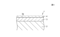
- FIG. 1 is a partial cross-sectional view of an electrical contact surface-treated with a surface treatment agent for electrical contact according to an embodiment of the present invention.
- the 1 includes a conductive portion 2 and a protective layer 3 thereon.
- a conductive metal or metal alloy is preferably used, and for example, Ni (nickel) or a Ni alloy can be used.
- the protective layer 3 is formed by coating a platinum group metal such as Au or a highly conductive metal such as Ag by plating or the like.
- the surface 3a of the protective layer 3 is a contact surface with an electrode formed of electronic component solder.
- a solder transfer preventing layer 4 is formed on the surface 3a of the protective layer 3.
- the protective layer 3 and the electrodes of the electronic component are electrically connected via the solder transfer preventing layer 4.
- the solder transfer preventing layer 4 is formed by removing the solvent component (C) in the treatment agent after providing the surface treatment agent for electrical contacts of the present embodiment on the surface 3a of the protective layer 3.
- the surface treatment agent for electrical contacts of the present embodiment is provided on the surface 3a of the protective layer 3 by, for example, a method such as coating or spraying, and then the solder transfer preventing layer 4 is formed by, for example, heating the electrical contacts. Is done. If the solvent component (C) is not completely removed, it may cause contact failure. Therefore, it is preferable to heat the electrical contacts at 40 to 100 ° C.
- the film thickness of the solder transfer preventing layer 4 is 0.05 to 100 ⁇ m. If the film thickness is larger than 100 ⁇ m, contact failure tends to occur, and if it is smaller than 0.05 ⁇ m, solder transfer cannot be prevented properly.
- the electrical contact of the present invention can be used as an elastic contact, for example.
- the example used for the connection apparatus provided with the electrical contact which has an elastic arm as an example of an elastic contact is shown.
- FIG. 2 is a partial cross-sectional view of the connection device using the electrical contact of the present invention
- FIG. 3 is an enlarged cross-sectional view showing the vicinity of the electrical contact of the connection device shown in FIG.
- the planar shape of the base 10 is, for example, a quadrangular shape, and side walls 10 a that rise substantially vertically are formed on each of the four sides of the base 10.
- a region surrounded by the four side wall portions 10 a is a concave portion, and the upper surface of the bottom portion 10 b is the support surface 12.
- a connection sheet 15 is installed on the support surface 12.
- the connection sheet 15 has a configuration in which, for example, a plurality of electrical contacts (contactors) 20 are provided on the surface of the flexible base sheet 16.
- a large number of through holes 16a are formed in the base sheet 16, and a conductor layer 17 is formed on the inner peripheral surface of each through hole 16a by means such as plating.
- a front-side connection land 17 a that conducts to the conductor layer 17 is formed on the surface of the base material sheet 16, and a back-side connection land 17 b that conducts to the conductor layer 17 is formed on the back surface of the base material sheet 16.
- the electrical contacts 20 are formed, for example, by punching a thin conductive metal plate, and further plated, and each electrical contact 20 is joined to the surface of the connection land 17a with a conductive adhesive or the like. .
- the electrical contact 20 is formed by a plating process using a conductive material such as copper or nickel.
- a plurality of electrical contacts 20 are formed on the surface of a sheet separate from the base sheet 16 by a plating process, the sheets are superimposed on the base sheet 16, and each electrical contact 20 is made of a conductive adhesive or the like. To be joined to the connection land 17a.
- Each electrical contact 20 is formed in a three-dimensional shape, for example, by applying an external force after being installed on the base sheet 16. At this time, the internal residual stress is removed by the heat treatment, and the electrical contact 20 can exhibit an elastic force in a three-dimensional shape.
- bump electrodes 18 made of a conductive material that are individually connected to the connection lands 17b are formed. As shown in FIG. 2, when the connection sheet 15 is installed on the support surface 12 that is the surface of the bottom 10 b of the base 10, the bump electrode 18 is connected to the conductive portion provided on the support surface 12.
- the arrangement pitch of the electrical contacts 20 on the support surface 12 is, for example, 2 mm or less, or 1 mm or less.
- the maximum value of the external dimension of the electrical contact 20 is also 2 mm or less, or 1 mm or less.
- connection sheet 15 is an example.
- the through hole 16a is provided in the base material sheet 16 in FIG. 3, the through hole 16a may not be formed and a wiring pattern that is electrically connected to the electrical contact 20 may be formed on the surface of the base material sheet 16. .
- the electrical contact 20 has a support portion 21 and an elastic arm 22 formed integrally and continuously.
- the elastic arm 22 is formed in, for example, a spiral shape, and the base end portion that is the winding start end of the elastic arm 22 is integrated with the support portion 21, and the distal end portion 22 b that is the winding end of the elastic arm 22 is substantially the spiral shape.
- the support portion 21 constituting the electrical contact 20 is connected to the connection land 17 a, and the elastic arm 22 is three-dimensionally molded so that the tip end portion 22 b is separated from the support surface 12.
- an electronic component 40 is installed in the connection device 9.
- the electronic component 40 is an IC package or the like, and various electronic elements such as an IC bare chip are sealed in the main body 41.
- a plurality of protruding electrodes 42 having solder on at least the surface are provided on the bottom surface 41 a of the main body 41, and each protruding electrode 42 is electrically connected to a circuit in the main body 41.
- the protruding electrode 42 has a spherical shape.
- the protruding electrode 42 may have a truncated cone shape.
- the connection device 9 is, for example, for inspecting the electronic component 40, and as shown in FIG. 2, the electronic component 40 which is an object to be inspected is mounted in the recess of the base 10. At this time, the electronic component 40 is positioned so that the individual protruding electrodes 42 provided on the bottom surface 41 a of the main body 41 are placed on the electrical contacts 20.
- a pressing lid (not shown) is provided on the base 10. When the lid is placed on the base 10, the electronic component 40 is pressed in the direction of arrow F by the lid. . Due to this pressing force, each protruding electrode 42 is pressed against the elastic arm 22, the three-dimensional elastic arm 22 is crushed, and the protruding electrode 42 and the elastic arm 22 are individually connected to each other. An operation test of the circuit in the main body 41 is performed to determine whether or not the circuit in the circuit 41 is disconnected.
- the electrical contact 20 is repeatedly brought into contact with the protruding electrode 42 by the pressing force.
- solder transfer is prevented on the surface of the electrical contact.
- Layer 4 is formed, and solder transfer can be effectively prevented.
- the electrical contact 20 and the protruding electrode 42 are in contact with each other by the pressing force, when the surface treatment is performed with the surface treatment agent for electrical contact of the present embodiment, good contact can be obtained even with a small load.
- Example 1 6.5 parts by weight of hydrofluorocarbon and 93.5 parts by weight of bis (trifluoromethyl) benzene were mixed to obtain a mixed solvent.
- a mixed solvent 100 parts by weight of the solvent component (C)
- 0.05 part by weight of an acrylate homopolymer as a solid component (A) and 0.5 part by weight of perfluoropolyether as an oil component (B) are added, and 10 to 10 parts at room temperature.
- the mixture was stirred for 30 minutes to obtain a surface treatment agent for electrical contacts (Example 1).
- the solid component (A) was dissolved in the solvent component (C) without being separated from the oil component (B).
- the acrylate homopolymer was a polymer of an acrylate polymer having a perfluoroalkyl group having 6 carbon atoms, and FTtronic FK6100H (manufactured by Eftron) having a molecular weight (number average molecular weight) of 50,000 to 150,000 was used. Further, Fomblin (registered trademark, manufactured by Solvay) was used as the perfluoropolyether.
- Example 2 With respect to 100 parts by weight of a mixed solvent (C) obtained by mixing 7.0 parts by weight of hydrofluorocarbon and 93.0 parts by weight of bis (trifluoromethyl) benzene, 0.05 part by weight of a methacrylate homopolymer as a solid component (A); As an oil component (B), 0.5 part by weight of perfluoropolyether was added to obtain a surface treatment agent for electrical contacts in the same manner as in Example 1 (Example 2).
- a mixed solvent (C) obtained by mixing 7.0 parts by weight of hydrofluorocarbon and 93.0 parts by weight of bis (trifluoromethyl) benzene, 0.05 part by weight of a methacrylate homopolymer as a solid component (A);
- an oil component (B) 0.5 part by weight of perfluoropolyether was added to obtain a surface treatment agent for electrical contacts in the same manner as in Example 1 (Example 2).
- the methacrylate homopolymer was a polymer of a methacrylate polymer having a C6 perfluoroalkyl group, and FTtronic FK6100M (manufactured by EFRON) having a molecular weight (number average molecular weight) of 50,000 to 150,000 was used. Further, the same Fomblin (registered trademark, manufactured by Solvay) as in Example 1 was used as the perfluoropolyether.
- Example 3 0.05 parts by weight of a copolymer of acrylate and methacrylate as a solid component (A) with respect to 100 parts by weight of a mixed solvent (C) in which 7.0 parts by weight of hydrofluorocarbon and 93.0 parts by weight of bis (trifluoromethyl) benzene are mixed. Then, 0.5 parts by weight of perfluoropolyether was added as an oil component (B) to obtain a surface treatment agent for electrical contacts in the same manner as in Example 1 (Example 3).
- the copolymer was a copolymer of an acrylate polymer and a methacrylate polymer having a perfluoroalkyl group having 6 carbon atoms, and FTtronic FK6100 (manufactured by EFRON) having a molecular weight (number average molecular weight) of 50,000 to 150,000 was used. Moreover, demnam (registered trademark, manufactured by Daikin Industries, Ltd.) was used as the perfluoropolyether.
- Example 4 With respect to 100 parts by weight of a mixed solvent (C) obtained by mixing 10.0 parts by weight of hydrofluorocarbon and 90.0 parts by weight of bis (trifluoromethyl) benzene, 0.07 part by weight of an acrylate homopolymer as a solid component (A); A surface treatment agent for electrical contacts was obtained in the same manner as in Example 1 by adding 1.0 part by weight of perfluoropolyether as the oil component (B) (Example 4).
- a mixed solvent (C) obtained by mixing 10.0 parts by weight of hydrofluorocarbon and 90.0 parts by weight of bis (trifluoromethyl) benzene, 0.07 part by weight of an acrylate homopolymer as a solid component (A);
- a surface treatment agent for electrical contacts was obtained in the same manner as in Example 1 by adding 1.0 part by weight of perfluoropolyether as the oil component (B) (Example 4).
- the acrylate homopolymer is the same acrylate polymer having a C6 perfluoroalkyl group as in Example 1, and EFtronic FK6100H (manufactured by EFRON) having a molecular weight (number average molecular weight) of 50,000 to 150,000 is used. It was. The same demnum (registered trademark, manufactured by Daikin Industries, Ltd.) as in Example 3 was used as the perfluoropolyether.
- Example 5 For 100 parts by weight of a mixed solvent obtained by mixing 7.0 parts by weight of hydrofluorocarbon and 93.0 parts by weight of bis (trifluoromethyl) benzene, 0.10 parts by weight of an acrylate homopolymer as a solid component (A), and an oil component ( As B), 0.5 part by weight of perfluorocarbon was added to obtain a surface treatment agent for electrical contacts in the same manner as in Example 1 (Example 5).
- the acrylate homopolymer is the same acrylate polymer having a C6 perfluoroalkyl group as in Example 1, and EFtronic FK6100H (manufactured by EFRON) having a molecular weight (number average molecular weight) of 50,000 to 150,000 is used. It was. In addition, Fluorinert (registered trademark, manufactured by 3M) was used as the perfluorocarbon.
- Example 6 To 100 parts by weight of a mixed solvent (C) obtained by mixing 6.0 parts by weight of hydrofluorocarbon and 94.0 parts by weight of bis (trifluoromethyl) benzene, 0.10 parts by weight of an acrylate homopolymer as a solid component (A); A surface treatment agent for electrical contacts was obtained in the same manner as in Example 1 by adding 0.1 part by weight of perfluoropolyether as the oil component (B) (Example 6).
- a mixed solvent (C) obtained by mixing 6.0 parts by weight of hydrofluorocarbon and 94.0 parts by weight of bis (trifluoromethyl) benzene, 0.10 parts by weight of an acrylate homopolymer as a solid component (A);
- a surface treatment agent for electrical contacts was obtained in the same manner as in Example 1 by adding 0.1 part by weight of perfluoropolyether as the oil component (B) (Example 6).
- the acrylate homopolymer is the same acrylate polymer having a C6 perfluoroalkyl group as in Example 1, and EFtronic FK6100H (manufactured by EFRON) having a molecular weight (number average molecular weight) of 50,000 to 150,000 is used. It was.
- the same perfluoropolyether as Fomblin (registered trademark, manufactured by Solvay) as in Example 1 was used.
- Comparative Example 1 Add only 0.05 parts by weight of acrylate homopolymer as the solid component (A) to 100.0 parts by weight of bis (trifluoromethyl) benzene as the solvent component (C), and stir and mix in the same manner as in Example 1. A surface treatment material for electrical contacts was obtained (Comparative Example 1).
- the acrylate homopolymer is the same acrylate polymer having a C6 perfluoroalkyl group as in Example 1, and EFtronic FK6100H (manufactured by EFRON) having a molecular weight (number average molecular weight) of 50,000 to 150,000 is used. It was.
- the methacrylate homopolymer was a polymer of a methacrylate polymer having a perfluoroalkyl group having 6 carbon atoms as in Example 2, and FTtronic FK6100M (manufactured by EFRON) having a molecular weight (number average molecular weight) of 50,000 to 150,000 was used. . Further, the same Fomblin (registered trademark, manufactured by Solvay) as in Example 1 was used as the perfluoropolyether. Table 1 shows the weight ratio of each component in Examples 1 to 6 and Comparative Examples 1 and 2.
- Test method The surface treatment agents for electric contacts of Examples 1 to 6 and Comparative Examples 1 and 2 were applied to the surface of the electric contact 20 of the connecting device 9 shown in FIGS. 2 and 3, and heated at 60 ° C. for solvent component (C ) Was removed.
- the test solder ball substrate was inserted into and removed from this connection device 20,000 times at a temperature of 85 ° C.
- the same insertion / extraction test was performed on the surface of the electrical contact 20 that was not coated with the surface treatment agent for electrical contact (Comparative Example 3) and the surface of the electrical contact 20 that was vacuum-deposited with titanium nitride (Comparative Example 4). It was.
- ⁇ The change of the average value of the measured value after the test with respect to the average value of the measured value before the test is 30 to 50%.
- X The change of the average value of the measured value after the test with respect to the average value of the measured value before the test is 50% or more.
- Table 2 shows the contact resistance values before and after the insertion / extraction test and the results of solder transfer after the insertion / extraction test for Examples 1 to 6 and Comparative Examples 1 to 4.
Landscapes
- Chemical & Material Sciences (AREA)
- Chemical Kinetics & Catalysis (AREA)
- General Chemical & Material Sciences (AREA)
- Oil, Petroleum & Natural Gas (AREA)
- Organic Chemistry (AREA)
- Lubricants (AREA)
- Other Surface Treatments For Metallic Materials (AREA)
- Paints Or Removers (AREA)
Abstract
Description
(ここで式中n=1~6の整数、R1はCmH2mであってm=1~10のアルキレン基またはフェニレン基、XはH、CH3、ClまたはF)
ここで-CnF2n+1で表されるパーフルオロアルキル基は、炭素数(n)に制限はなく、例えばn=7以上など炭素数が大きいものも用いることができる。しかしながら近年、n=7以上のパーフルオロアルキル基を含む化合物は環境へ与える負荷が大きいことが懸念されており、炭素数の小さなパーフルオロアルキル基を含む化合物の使用が求められている。そこで、本実施の形態では、n=1~6のパーフルオロアルキル基を含むものとした。n=1~6のパーフルオロアルキル基は、側鎖を有するもの、直鎖状のもの、いずれも用いることができる。炭素数の大きいパーフルオロアルキル基を含む化合物ははんだ転写を抑制する効果が高いことから、n=5~6のパーフルオロアルキル基、特にn=6のパーフルオロアルキル基を用いることが好ましい。
ハイドロフルオロカーボン6.5重量部とビス(トリフルオロメチル)ベンゼン93.5重量部を混合し、混合溶媒とした。この溶媒成分(C)100重量部に対し、固体成分(A)としてアクリレートホモポリマー0.05重量部と、オイル成分(B)としてパーフルオロポリエーテル0.5重量部を加え、室温で10~30分攪拌混合し、電気接点用表面処理剤を得た(実施例1)。この電気接点用表面処理剤は、固体成分(A)がオイル成分(B)と分離することなく、ともに溶媒成分(C)に溶解していた。前記アクリレートホモポリマーは炭素数6のパーフルオロアルキル基を有するアクリレートポリマーの重合体で、分子量(数平均分子量)は50000~150000であるエフトロニックFK6100H(エフトロン社製)を用いた。また、前記パーフルオロポリエーテルとしてフォンブリン(登録商標,ソルベイ社製)を用いた。
ハイドロフルオロカーボン7.0重量部とビス(トリフルオロメチル)ベンゼン93.0重量部を混合した混合溶媒(C)100重量部に対し、固体成分(A)としてメタクリレートホモポリマー0.05重量部と、オイル成分(B)としてパーフルオロポリエーテル0.5重量部を加えて実施例1と同様にして電気接点用表面処理剤を得た(実施例2)。前記メタクリレートホモポリマーは炭素数6のパーフルオロアルキル基を有するメタクリレートポリマーの重合体で、分子量(数平均分子量)は50000~150000であるエフトロニックFK6100M(エフトロン社製)を用いた。また、前記パーフルオロポリエーテルとして実施例1と同じフォンブリン(登録商標,ソルベイ社製)を用いた。
ハイドロフルオロカーボン7.0重量部とビス(トリフルオロメチル)ベンゼン93.0重量部を混合した混合溶媒(C)100重量部に対し、固体成分(A)としてアクリレートとメタクリレートのコポリマー0.05重量部と、オイル成分(B)としてパーフルオロポリエーテル0.5重量部を加えて実施例1と同様にして電気接点用表面処理剤を得た(実施例3)。前記コポリマーは炭素数6のパーフルオロアルキル基を有するアクリレートポリマーとメタクリレートポリマーの共重合体で、分子量(数平均分子量)は50000~150000であるエフトロニックFK6100(エフトロン社製)を用いた。また、前記パーフルオロポリエーテルとしてデムナム(登録商標,ダイキン工業社製)を用いた。
ハイドロフルオロカーボン10.0重量部とビス(トリフルオロメチル)ベンゼン90.0重量部を混合した混合溶媒(C)100重量部に対し、固体成分(A)としてアクリレートホモポリマー0.07重量部と、オイル成分(B)としてパーフルオロポリエーテル1.0重量部を加えて実施例1と同様にして電気接点用表面処理剤を得た(実施例4)。前記アクリレートホモポリマーは実施例1と同じ、炭素数6のパーフルオロアルキル基を有するアクリレートポリマーの重合体で、分子量(数平均分子量)は50000~150000であるエフトロニックFK6100H(エフトロン社製)を用いた。また、前記パーフルオロポリエーテルとして実施例3と同じデムナム(登録商標,ダイキン工業社製)を用いた。
ハイドロフルオロカーボン7.0重量部とビス(トリフルオロメチル)ベンゼン93.0重量部を混合した混合溶媒100重量部に対し、固体成分(A)としてアクリレートホモポリマー0.10重量部と、オイル成分(B)としてパーフルオロカーボン0.5重量部を加えて実施例1と同様にして電気接点用表面処理剤を得た(実施例5)。前記アクリレートホモポリマーは実施例1と同じ、炭素数6のパーフルオロアルキル基を有するアクリレートポリマーの重合体で、分子量(数平均分子量)は50000~150000であるエフトロニックFK6100H(エフトロン社製)を用いた。また、前記パーフルオロカーボンとしてフロリナート(登録商標,スリーエム社製)を用いた。
ハイドロフルオロカーボン6.0重量部とビス(トリフルオロメチル)ベンゼン94.0重量部を混合した混合溶媒(C)100重量部に対し、固体成分(A)としてアクリレートホモポリマー0.10重量部と、オイル成分(B)としてパーフルオロポリエーテル0.1重量部を加えて実施例1と同様にして電気接点用表面処理剤を得た(実施例6)。前記アクリレートホモポリマーは実施例1と同じ、炭素数6のパーフルオロアルキル基を有するアクリレートポリマーの重合体で、分子量(数平均分子量)は50000~150000であるエフトロニックFK6100H(エフトロン社製)を用いた。また、前記パーフルオロポリエーテルとして、実施例1と同じフォンブリン(登録商標,ソルベイ社製)を用いた。
溶媒成分(C)としてビス(トリフルオロメチル)ベンゼン100.0重量部に対し、固体成分(A)としてアクリレートホモポリマー0.05重量部のみを加え、実施例1と同様にして攪拌混合し、電気接点用表面処理材を得た(比較例1)。前記アクリレートホモポリマーは実施例1と同じ、炭素数6のパーフルオロアルキル基を有するアクリレートポリマーの重合体で、分子量(数平均分子量)は50000~150000であるエフトロニックFK6100H(エフトロン社製)を用いた。
ハイドロフルオロカーボン10.0重量部とビス(トリフルオロメチル)ベンゼン90.0重量部を混合した混合溶媒(C)100重量部に対し、固体成分(A)としてメタクリレートホモポリマー8.00重量部と、オイル成分(B)としてパーフルオロポリエーテル1.0重量部を加えて実施例1と同様にして電気接点用表面処理剤を得た(比較例2)。前記メタクリレートホモポリマーは実施例2と同じ炭素数6のパーフルオロアルキル基を有するメタクリレートポリマーの重合体で、分子量(数平均分子量)は50000~150000であるエフトロニックFK6100M(エフトロン社製)を用いた。また、前記パーフルオロポリエーテルとして実施例1と同じフォンブリン(登録商標,ソルベイ社製)を用いた。
表1に実施例1~6および比較例1,2における各成分の重量比を示す。

実施例1~6、および比較例1,2の電気接点用表面処理剤を、図2および3に示す接続装置9の電気接点20表面に塗付し、60℃で加熱して溶媒成分(C)を除去した。この接続装置に、試験用はんだボール基板を温度85℃において、2万回挿抜させた。また、電気接点20表面に電気接点用表面処理剤を塗付しないもの(比較例3)、電気接点20表面に窒化チタンを真空蒸着したもの(比較例4)について、それぞれ同様の挿抜試験を行った。
A.接触抵抗値
前記挿抜試験を行う前、および行った後それぞれについて、電気接点間の電圧を測定し、電圧降下の値によって接触抵抗値を求め、以下のように評価をした。
〔試験前〕
◎:接触抵抗値のばらつきが10%以下
〇:接触抵抗値のばらつきが10~30%
△:接触抵抗値のばらつきが30~50%
×:接触抵抗値のばらつきが50%以上
〔試験後〕
◎:試験前の測定値の平均値と試験後の測定値の平均値と変わらない
〇:試験前の測定値の平均値に対する試験後の測定値の平均値の変化が10~30%
△:試験前の測定値の平均値に対する試験後の測定値の平均値の変化が30~50%
×:試験前の測定値の平均値に対する試験後の測定値の平均値の変化が50%以上
電子顕微鏡を用いて、前記挿抜試験を行った後の電気接点の表面におけるはんだの移着状態を観察し、以下のように評価した。
◎:はんだが移着した痕跡が認められなかった
〇:はんだが移着した痕跡が1mm2当り1~2点認められた
△:はんだが移着した痕跡が1mm2当り数点認められた
×:はんだが移着した顕著な痕跡が認められた

2 導電部
3 保護層
4 はんだ転写防止層
9 接続装置
10 基台
10a 基台の側壁部
10b 基台の底部
12 支持面
15 接続シート
16 基材シート
16a スルーホール
17 導電体層
17b 接続ランド
18 バンプ電極
21 支持部
22 弾性腕
40 電子部品
41 電子部品の本体部
41a 本体部の底面
42 突出電極
Claims (12)
- (A)炭素数6以下のパーフルオロアルキル基を含むアクリレートおよびメタクリレートから選ばれるモノマーの付加重合ポリマーである固体成分と、
(B)フッ素系オイルと、
(C)フッ素系溶媒と、
を含有することを特徴とする電気接点用表面処理剤。 - 前記アクリレートおよびメタクリレートは下記一般式(1)で表される請求項1に記載の電気接点用表面処理剤。
CH2=CXCOOR1CnF2n+1 式(1)
(ここで式中n=1~6の整数、R1はCmH2mであってm=1~10のアルキレン基またはフェニレン基、XはH、CH3、ClまたはF) - 前記(C)100重量部に対し、前記(A)を0.01~5.0重量部、前記(B)を0.01~5.0重量部含む請求項1または2記載の電気接点用表面処理剤。
- 前記(A)は前記一般式(1)で表されるアクリレートおよびメタアクリレートから選ばれるモノマーの単独成分からなる付加重合物である請求項2記載の電気接点表面処理剤。
- 前記(A)は前記一般式(1)で表されるアクリレートおよびメタアクリレートから選ばれるモノマーと、オルガノアルキル基を含むアクリレートおよびメタアクリレートから選ばれるモノマーとの共付加重合物である請求項2記載の電気接点表面処理剤。
- 前記(A)は前記一般式(1)で表されるアクリレートとメタアクリレートとの共付加重合物である請求項2記載の電気接点表面処理剤。
- 前記(B)は、ハイドロフルオロエーテル、パーフルオロカーボン、ハイドロフルオロカーボン、パーフルオロポリエーテル、ハイドロフルオロポリエーテルから選ばれるいずれかを含む請求項1に記載の電気接点用表面処理剤。
- 前記(B)はパーフルオロポリエーテルである請求項7の電気接点用表面処理剤。
- 前記(C)は、ハイドロフルオロエーテル、パーフルオロカーボン、ハイドロフルオロカーボン、パーフルオロポリエーテル、ハイドロフルオロポリエーテル、ベンゾトリフルオライド、ビス(トリフルオロメチル)ベンゼンから選ばれるいずれかを含む請求項1または7に記載の電気接点用表面処理剤。
- 前記(C)は、ハイドロフルオロカーボンとビス(トリフルオロメチル)ベンゼンとの混合溶媒である請求項9記載の電気接点用表面処理剤。
- 前記混合溶媒中のハイドロフルオロカーボンとビス(トリフルオロメチル)ベンゼンとの重量比が1:10~1:25の範囲である請求項10記載の電気接点用表面処理剤。
- 請求項1または7に記載の電気接点用表面処理剤を塗付することを特徴とする電気接点の表面処理方法。
Priority Applications (2)
| Application Number | Priority Date | Filing Date | Title |
|---|---|---|---|
| CN2011800097355A CN102782105A (zh) | 2010-02-26 | 2011-02-10 | 电触头用表面处理剂 |
| JP2012501734A JPWO2011105223A1 (ja) | 2010-02-26 | 2011-02-10 | 電気接点用表面処理剤 |
Applications Claiming Priority (2)
| Application Number | Priority Date | Filing Date | Title |
|---|---|---|---|
| JP2010041313 | 2010-02-26 | ||
| JP2010-041313 | 2010-02-26 |
Publications (1)
| Publication Number | Publication Date |
|---|---|
| WO2011105223A1 true WO2011105223A1 (ja) | 2011-09-01 |
Family
ID=44506637
Family Applications (1)
| Application Number | Title | Priority Date | Filing Date |
|---|---|---|---|
| PCT/JP2011/052819 Ceased WO2011105223A1 (ja) | 2010-02-26 | 2011-02-10 | 電気接点用表面処理剤 |
Country Status (3)
| Country | Link |
|---|---|
| JP (1) | JPWO2011105223A1 (ja) |
| CN (1) | CN102782105A (ja) |
| WO (1) | WO2011105223A1 (ja) |
Cited By (2)
| Publication number | Priority date | Publication date | Assignee | Title |
|---|---|---|---|---|
| JP2013151648A (ja) * | 2011-12-26 | 2013-08-08 | Agc Seimi Chemical Co Ltd | 混合溶剤および表面処理剤 |
| JP2018199782A (ja) * | 2017-05-26 | 2018-12-20 | Nokクリューバー株式会社 | 潤滑剤組成物 |
Citations (5)
| Publication number | Priority date | Publication date | Assignee | Title |
|---|---|---|---|---|
| JPS6049859A (ja) * | 1983-08-30 | 1985-03-19 | Asahi Glass Co Ltd | 半田用フラツクスの這上り防止剤 |
| JPH1133708A (ja) * | 1997-07-15 | 1999-02-09 | Seimi Chem Co Ltd | 半田用フラックス這い上がり防止剤、該防止剤組成物およびその用途 |
| JP2001135926A (ja) * | 1999-11-02 | 2001-05-18 | Seimi Chem Co Ltd | 半田用フラックス這い上がり防止剤組成物とその用途 |
| WO2007099760A1 (ja) * | 2006-03-01 | 2007-09-07 | Agc Seimi Chemical Co., Ltd. | 半田用フラックス這い上がり防止組成物 |
| WO2009090798A1 (ja) * | 2008-01-18 | 2009-07-23 | Agc Seimi Chemical Co., Ltd. | はんだ用フラックス這い上がり防止組成物、該組成物を被覆したはんだ用電子部材、該部材のはんだ付け方法および電気製品 |
Family Cites Families (2)
| Publication number | Priority date | Publication date | Assignee | Title |
|---|---|---|---|---|
| EP0191882B1 (en) * | 1985-02-21 | 1989-06-07 | Asahi Glass Company Ltd. | Method for soldering an electrical product |
| ITMI20062310A1 (it) * | 2006-11-30 | 2008-06-01 | Solvay Solexis Spa | Lubrificanti fluorurati |
-
2011
- 2011-02-10 WO PCT/JP2011/052819 patent/WO2011105223A1/ja not_active Ceased
- 2011-02-10 JP JP2012501734A patent/JPWO2011105223A1/ja not_active Withdrawn
- 2011-02-10 CN CN2011800097355A patent/CN102782105A/zh active Pending
Patent Citations (5)
| Publication number | Priority date | Publication date | Assignee | Title |
|---|---|---|---|---|
| JPS6049859A (ja) * | 1983-08-30 | 1985-03-19 | Asahi Glass Co Ltd | 半田用フラツクスの這上り防止剤 |
| JPH1133708A (ja) * | 1997-07-15 | 1999-02-09 | Seimi Chem Co Ltd | 半田用フラックス這い上がり防止剤、該防止剤組成物およびその用途 |
| JP2001135926A (ja) * | 1999-11-02 | 2001-05-18 | Seimi Chem Co Ltd | 半田用フラックス這い上がり防止剤組成物とその用途 |
| WO2007099760A1 (ja) * | 2006-03-01 | 2007-09-07 | Agc Seimi Chemical Co., Ltd. | 半田用フラックス這い上がり防止組成物 |
| WO2009090798A1 (ja) * | 2008-01-18 | 2009-07-23 | Agc Seimi Chemical Co., Ltd. | はんだ用フラックス這い上がり防止組成物、該組成物を被覆したはんだ用電子部材、該部材のはんだ付け方法および電気製品 |
Cited By (2)
| Publication number | Priority date | Publication date | Assignee | Title |
|---|---|---|---|---|
| JP2013151648A (ja) * | 2011-12-26 | 2013-08-08 | Agc Seimi Chemical Co Ltd | 混合溶剤および表面処理剤 |
| JP2018199782A (ja) * | 2017-05-26 | 2018-12-20 | Nokクリューバー株式会社 | 潤滑剤組成物 |
Also Published As
| Publication number | Publication date |
|---|---|
| CN102782105A (zh) | 2012-11-14 |
| JPWO2011105223A1 (ja) | 2013-06-20 |
Similar Documents
| Publication | Publication Date | Title |
|---|---|---|
| US10056707B2 (en) | Electrical contact including corrosion-resistant coating | |
| US20120138868A1 (en) | Circuit connecting material, film-like circuit connecting material using the circuit connecting material, structure for connecting circuit member, and method for connecting circuit member | |
| JP6224090B2 (ja) | 電子部品 | |
| CN105281076A (zh) | 连接器 | |
| JP2007184142A (ja) | フラットケーブル | |
| KR101561418B1 (ko) | 도전성 미립자, 이방성 도전 재료 및 도전 접속 구조체 | |
| JP4313836B2 (ja) | 導電性微粒子、異方性導電材料、及び、導電接続構造体 | |
| WO2011105223A1 (ja) | 電気接点用表面処理剤 | |
| JP2019044043A (ja) | 回路接続用接着剤組成物及び構造体 | |
| US20230006386A1 (en) | Contact member, connector, composition, and method for producing contact member | |
| US20170085016A1 (en) | Press-fit terminal | |
| CN101952082A (zh) | 焊剂上爬防止组合物、被覆了该组合物的锡焊用电子构件、该构件的锡焊方法及电气产品 | |
| JP2005019103A (ja) | コネクタ接点材料および多極端子 | |
| JP4441817B2 (ja) | 回路基板 | |
| JP7839258B2 (ja) | 導電性粒子 | |
| JP7733583B2 (ja) | 導電性粒子、ソケット、導電材料及び接続構造体 | |
| JP5360586B2 (ja) | 嵌合型接続端子 | |
| JP6805547B2 (ja) | プレスフィット端子 | |
| JP2010174096A (ja) | 異方性導電接着剤 | |
| JP6868467B2 (ja) | 潤滑剤組成物 | |
| JP2023079632A (ja) | 接続構造体、及び接続構造体の製造方法 | |
| WO2023090115A1 (ja) | 配線基板 | |
| JP2023079630A (ja) | 接続構造体の製造方法及び接続構造体 |
Legal Events
| Date | Code | Title | Description |
|---|---|---|---|
| WWE | Wipo information: entry into national phase |
Ref document number: 201180009735.5 Country of ref document: CN |
|
| 121 | Ep: the epo has been informed by wipo that ep was designated in this application |
Ref document number: 11747187 Country of ref document: EP Kind code of ref document: A1 |
|
| WWE | Wipo information: entry into national phase |
Ref document number: 2012501734 Country of ref document: JP |
|
| NENP | Non-entry into the national phase |
Ref country code: DE |
|
| 122 | Ep: pct application non-entry in european phase |
Ref document number: 11747187 Country of ref document: EP Kind code of ref document: A1 |