WO2011102240A1 - インプリント方法 - Google Patents
インプリント方法 Download PDFInfo
- Publication number
- WO2011102240A1 WO2011102240A1 PCT/JP2011/052346 JP2011052346W WO2011102240A1 WO 2011102240 A1 WO2011102240 A1 WO 2011102240A1 JP 2011052346 W JP2011052346 W JP 2011052346W WO 2011102240 A1 WO2011102240 A1 WO 2011102240A1
- Authority
- WO
- WIPO (PCT)
- Prior art keywords
- molding material
- resist
- pattern
- mold
- pressing
- Prior art date
- Legal status (The legal status is an assumption and is not a legal conclusion. Google has not performed a legal analysis and makes no representation as to the accuracy of the status listed.)
- Ceased
Links
Images


Classifications
-
- H—ELECTRICITY
- H10—SEMICONDUCTOR DEVICES; ELECTRIC SOLID-STATE DEVICES NOT OTHERWISE PROVIDED FOR
- H10P—GENERIC PROCESSES OR APPARATUS FOR THE MANUFACTURE OR TREATMENT OF DEVICES COVERED BY CLASS H10
- H10P76/00—Manufacture or treatment of masks on semiconductor bodies, e.g. by lithography or photolithography
- H10P76/20—Manufacture or treatment of masks on semiconductor bodies, e.g. by lithography or photolithography of masks comprising organic materials
- H10P76/204—Manufacture or treatment of masks on semiconductor bodies, e.g. by lithography or photolithography of masks comprising organic materials of organic photoresist masks
- H10P76/2041—Photolithographic processes
-
- B—PERFORMING OPERATIONS; TRANSPORTING
- B29—WORKING OF PLASTICS; WORKING OF SUBSTANCES IN A PLASTIC STATE IN GENERAL
- B29C—SHAPING OR JOINING OF PLASTICS; SHAPING OF MATERIAL IN A PLASTIC STATE, NOT OTHERWISE PROVIDED FOR; AFTER-TREATMENT OF THE SHAPED PRODUCTS, e.g. REPAIRING
- B29C33/00—Moulds or cores; Details thereof or accessories therefor
- B29C33/44—Moulds or cores; Details thereof or accessories therefor with means for, or specially constructed to facilitate, the removal of articles, e.g. of undercut articles
-
- B—PERFORMING OPERATIONS; TRANSPORTING
- B29—WORKING OF PLASTICS; WORKING OF SUBSTANCES IN A PLASTIC STATE IN GENERAL
- B29C—SHAPING OR JOINING OF PLASTICS; SHAPING OF MATERIAL IN A PLASTIC STATE, NOT OTHERWISE PROVIDED FOR; AFTER-TREATMENT OF THE SHAPED PRODUCTS, e.g. REPAIRING
- B29C33/00—Moulds or cores; Details thereof or accessories therefor
- B29C33/42—Moulds or cores; Details thereof or accessories therefor characterised by the shape of the moulding surface, e.g. ribs or grooves
- B29C33/424—Moulding surfaces provided with means for marking or patterning
-
- B—PERFORMING OPERATIONS; TRANSPORTING
- B29—WORKING OF PLASTICS; WORKING OF SUBSTANCES IN A PLASTIC STATE IN GENERAL
- B29C—SHAPING OR JOINING OF PLASTICS; SHAPING OF MATERIAL IN A PLASTIC STATE, NOT OTHERWISE PROVIDED FOR; AFTER-TREATMENT OF THE SHAPED PRODUCTS, e.g. REPAIRING
- B29C37/00—Component parts, details, accessories or auxiliary operations, not covered by group B29C33/00 or B29C35/00
- B29C37/0003—Discharging moulded articles from the mould
-
- B—PERFORMING OPERATIONS; TRANSPORTING
- B29—WORKING OF PLASTICS; WORKING OF SUBSTANCES IN A PLASTIC STATE IN GENERAL
- B29C—SHAPING OR JOINING OF PLASTICS; SHAPING OF MATERIAL IN A PLASTIC STATE, NOT OTHERWISE PROVIDED FOR; AFTER-TREATMENT OF THE SHAPED PRODUCTS, e.g. REPAIRING
- B29C59/00—Surface shaping of articles, e.g. embossing; Apparatus therefor
- B29C59/02—Surface shaping of articles, e.g. embossing; Apparatus therefor by mechanical means, e.g. pressing
- B29C59/022—Surface shaping of articles, e.g. embossing; Apparatus therefor by mechanical means, e.g. pressing characterised by the disposition or the configuration, e.g. dimensions, of the embossments or the shaping tools therefor
-
- B—PERFORMING OPERATIONS; TRANSPORTING
- B82—NANOTECHNOLOGY
- B82Y—SPECIFIC USES OR APPLICATIONS OF NANOSTRUCTURES; MEASUREMENT OR ANALYSIS OF NANOSTRUCTURES; MANUFACTURE OR TREATMENT OF NANOSTRUCTURES
- B82Y10/00—Nanotechnology for information processing, storage or transmission, e.g. quantum computing or single electron logic
-
- B—PERFORMING OPERATIONS; TRANSPORTING
- B82—NANOTECHNOLOGY
- B82Y—SPECIFIC USES OR APPLICATIONS OF NANOSTRUCTURES; MEASUREMENT OR ANALYSIS OF NANOSTRUCTURES; MANUFACTURE OR TREATMENT OF NANOSTRUCTURES
- B82Y40/00—Manufacture or treatment of nanostructures
-
- G—PHYSICS
- G03—PHOTOGRAPHY; CINEMATOGRAPHY; ANALOGOUS TECHNIQUES USING WAVES OTHER THAN OPTICAL WAVES; ELECTROGRAPHY; HOLOGRAPHY
- G03F—PHOTOMECHANICAL PRODUCTION OF TEXTURED OR PATTERNED SURFACES, e.g. FOR PRINTING, FOR PROCESSING OF SEMICONDUCTOR DEVICES; MATERIALS THEREFOR; ORIGINALS THEREFOR; APPARATUS SPECIALLY ADAPTED THEREFOR
- G03F7/00—Photomechanical, e.g. photolithographic, production of textured or patterned surfaces, e.g. printing surfaces; Materials therefor, e.g. comprising photoresists; Apparatus specially adapted therefor
- G03F7/0002—Lithographic processes using patterning methods other than those involving the exposure to radiation, e.g. by stamping
-
- B—PERFORMING OPERATIONS; TRANSPORTING
- B29—WORKING OF PLASTICS; WORKING OF SUBSTANCES IN A PLASTIC STATE IN GENERAL
- B29C—SHAPING OR JOINING OF PLASTICS; SHAPING OF MATERIAL IN A PLASTIC STATE, NOT OTHERWISE PROVIDED FOR; AFTER-TREATMENT OF THE SHAPED PRODUCTS, e.g. REPAIRING
- B29C35/00—Heating, cooling or curing, e.g. crosslinking or vulcanising; Apparatus therefor
- B29C35/02—Heating or curing, e.g. crosslinking or vulcanizing during moulding, e.g. in a mould
- B29C35/08—Heating or curing, e.g. crosslinking or vulcanizing during moulding, e.g. in a mould by wave energy or particle radiation
- B29C35/0805—Heating or curing, e.g. crosslinking or vulcanizing during moulding, e.g. in a mould by wave energy or particle radiation using electromagnetic radiation
- B29C2035/0827—Heating or curing, e.g. crosslinking or vulcanizing during moulding, e.g. in a mould by wave energy or particle radiation using electromagnetic radiation using UV radiation
Definitions
- the present invention relates to an imprint method for transferring a reversal pattern of a molding material to a molding material by pressing the molding material on which the desired pattern is formed to the molding material.
- a desired pattern is generally formed on a base material using a lithography technique. Some have achieved further fine processing by lithography technology using a short wavelength laser or electron beam.
- the lithography technique requires multiple steps of transfer, exposure, and development. Further, lasers having a short wavelength such as ultraviolet rays are expensive to purchase and maintain, and have a problem that the apparatus becomes large and the exposure takes time, resulting in high costs.
- the imprint method requires a lot of time to separate the molding material from the molding material.
- the uneven pattern formed on the molding material is transferred to the molding material, the molding material is cured, and then the molding material is lifted and separated from the molding material. This is because it is not easily peeled off from the material to be molded.
- the number of wafers that can be processed in one hour is as small as about four, which has a problem in throughput.
- an object of the present invention is to provide a new and improved imprint method capable of quickly separating a molding material and a molding material in pattern formation.
- a transfer that transfers a reverse pattern of the molding material to the molding material by pressing the molding material on which the desired pattern is formed to the molding material.
- the peeling step includes a separation step of separating the molding material in a direction opposite to a pressing direction of the molding material, and a pressing step of pressing the molding material in the same direction as the pressing direction of the molding material.
- a peeling process including a pressing process and a separating process is performed. Specifically, the molding material is pulled away in the direction opposite to the pressing direction of the molding material in the separating step while pressing the molding material in the same direction as the pressing direction in the pressing step. At this time, the separating step and the peeling step may be performed in conjunction with each other or simultaneously.
- the stripping method that simply pulls the molding material away from the direction of crimping of the molding material takes a long time to peel it off. And it can be peeled off quickly. As a result, throughput during pattern formation can be improved.
- the molding material may be pressed in the same direction as the pressing direction of the molding material by passing a pin through a through hole provided in the molding material and contacting the molding material.
- a plurality of through-holes for the pins and the molding material are provided, and the arrangement of the plurality of pins that pass through the plurality of through-holes and come into contact with the molding material depends on the pattern density formed in the molding material. May be optimized.
- a plurality of through holes for the pins and the molding material may be provided, and the arrangement of the plurality of pins that pass through the plurality of through holes and come into contact with the molding material may be equally spaced.
- the length of the plurality of pins may be 5 times or more the thickness of the molding material.
- the imprint method includes at least one of semiconductor pattern formation, recording medium pattern formation, solar cell pattern formation, lens array pattern formation, photonic crystal device manufacture, and light-emitting diode antireflection film pattern formation. It may be used for
- the transfer step may be performed in an atmosphere of a gas that condenses at a temperature when the molding material enters the concave portion of the molding material and a pressure in the concave portion.
- Nanoimprinting is a microfabrication technique for transferring a nanometer-order pattern to a material to be molded by pressing a material called a mold against the material to be molded.
- the nanoimprint technique is used, for example, in place of a lithography technique that has been conventionally used for pattern formation during semiconductor manufacturing described below.
- Nanoimprint performs pattern transfer to a material to be molded as a series of steps including an alignment process, a crimping process, a transfer process, a mold release process, a pin retracting process, a mold and a pin moving process.
- the mold 10 is used as the molding material according to the present embodiment.
- the mold 10 is a quartz base material that transmits ultraviolet rays (UV), and has a desired uneven pattern formed on the surface thereof.
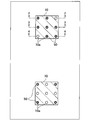
- FIG. 2 shows a cross section 1-1 of the mold 10 shown in the top view of FIG.
- the mold 10 has a square cross section and is provided with nine through holes 10a at equal intervals.
- a base material 20 such as a silicon substrate is used. Resin is applied to the substrate 20. Below, the said resin part formed on the base material 20 is also called the resist 30.
- the resist 30 may be a low-viscosity photo-curing resin that cures when irradiated with ultraviolet rays.
- the ⁇ positioning step> of the first step in FIG. 1 is executed.
- alignment of the mold 10 and the base material 20 in the XY direction (surface direction of the base material 20) is performed by a known method such as an optical method.
- the ⁇ crimping step> of the second step in FIG. 1 is performed.
- the pressure bonding step the mold 10 is lowered toward the base material 20, and the mold 10 is pressure bonded to the resist 30.
- the resist 30 enters the recess of the mold 10. In this way, the uneven pattern of the mold 10 is formed on the resist 30.
- the ⁇ mold release process (peeling process)> of the fourth process in FIG. 1 is performed.
- the mold release process includes an operation of separating the mold 10 in a direction opposite to the direction in which the resist 30 is pressed (here, the mold lowering direction) (a pulling process), and an operation of pressing the resist 30 in the same direction as the pressure of the mold 10 (pressing process). ) And.
- the mold 10 is peeled from the resist 30 by raising the mold 10 in the direction opposite to the direction in which the resist 30 is pressed as described above.
- the mold 10 is not easily peeled off. This has been the main factor that slows down the processing speed of pattern formation by the nanoimprint method.
- a pressing process is provided together with a separating process. This is executed by pressing a plurality of pins 50 against the resist 30 through the through holes 10 a provided in the mold 10.
- the timing of lowering the pin 50 may be after the resist 30 is cured or during irradiation with UV light. However, the timing at which the pin 50 is brought into contact with the resist 30 must be after the resist 30 is cured. Thus, the separation step and the pressing step are performed in conjunction with each other after the resist 30 is cured. The separating step and the pressing step may be performed almost simultaneously.
- the ⁇ pin retracting step> of the fifth step of FIG. 1 is executed.
- the pin retracting step when the mold 10 is completely separated from the resist 30, the pin 50 is raised above the mold 10, and the pin 50 is retracted so that the pin 50 does not get in the way when the mold 10 is moved.
- the mold 10 is pressed in the direction opposite to the pressing direction of the resist 30 while pressing the resist 30 in the same direction as the pressing direction by the pins 50. Pull apart.
- the resist 30 and the mold 10 which are difficult to be peeled off simply by pulling the mold 10 away in the direction opposite to the pressing direction of the resist 30 can be reliably and rapidly peeled off.
- the throughput at the time of pattern formation can be improved.
- Examples of the material of the pin 50 include aluminum and stainless steel.
- the tip of the pin 50 is made of, for example, a wholly aromatic polyimide resin or fluorine-containing resin excellent in friction resistance such as Vespel (registered trademark) so as not to damage the resist 30.
- the diameter of the pin 50 is formed in a size from micron order to milli order depending on the fineness of the pattern to be formed.
- the length of the pin 50 is 5 to 10 times the thickness of the mold 10.
- the arrangement of the pins 50 passing through the through holes 10a and coming into contact with the resist 30 is optimized according to the pattern density formed on the mold 10.
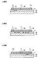
- the upper, middle, and lower views of FIG. 3 show the 2-2 cross section, 3-3 cross section, and 4-4 cross section of the mold 10 shown in the upper side of FIG.
- the pattern density of the mold 10 is dense on the left side of the drawing and sparse on the right side. Therefore, among the through holes 10a on the upper cutting line 2-2 in FIG. 2, the pins 50 are passed only from the left two through holes 10a, and as shown in the upper diagram of FIG.
- the resist 30 is pressed with the pin 50. In this way, the arrangement of the pins 50 that press the resist 30 is made denser in the left part having a high pattern density than in the right part having a low pattern density.
- the pattern density of the mold 10 is dense on both the left and right sides of the drawing. Accordingly, the pins 50 are passed through all of the through holes 10a on the upper 3-3 cutting line in FIG. 2, and the entire resist 30 is uniformly pressed by the three pins 50 as shown in the central view of FIG. . In this way, when the pattern density is uniformly high, the entire resist 30 is pressed evenly with the pins 50.
- the pattern density of the mold 10 is sparse on the left side of the drawing and dense on the right side. Accordingly, among the through holes 10a on the upper 4-4 cutting line of FIG. 2, the pins 50 are passed only from the two right through holes 10a, and as shown in the lower diagram of FIG. The resist 30 is pressed at 50. In this way, the arrangement of the pins 50 that press the resist 30 is made denser in the right part having a high pattern density than in the left part having a low pattern density.
- the arrangement of the plurality of pins 50 that pass through the plurality of through holes 10a and come into contact with the resist 30 depends on the pattern density formed on the mold 10. By optimizing, the mold 10 and the resist 30 can be peeled off reliably and rapidly.
- the arrangement of the plurality of pins 50 that contact the resist 30 through the plurality of through holes 10 a is made at equal intervals.
- four pins 50 pass through the through holes 10 a in the vicinity of the four corners of the mold 10 and come into contact with the resist 30 at equal intervals.
- the present invention is not limited to this, and for example, nine pins 50 may be pressed against the resist 30 from all nine through holes 10 a provided in the mold 10.
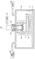
- FIG. 4 is a longitudinal sectional view showing the overall configuration of the pattern forming apparatus according to the present embodiment.
- the pattern forming apparatus 100 includes a processing container 105 in which a nanoimprint method is executed.
- the processing container 105 is provided with a sliding stage 115 on a surface plate 110.
- the sliding stage 115 freely slides in the horizontal plane. Thereby, the base material 20 (and the resist 30) on the sliding stage 115 moves horizontally.
- an elevating stage 120 is installed for elevating the mold 10 and pressing the uneven pattern formed on the lower surface of the mold 10 against the resist 30 positioned below the mold 10.
- the mold pressing mechanism (molding material pressing mechanism) 120a of the elevating stage 120 is operated, and the mold 10 is lowered.
- the mold 10 comes into close contact with the resist 30 due to the lowering, the uneven pattern on the lower surface of the mold 10 is pressed against the resist 30, and the uneven pattern of the mold 10 is formed in the softened resist 30.
- ultraviolet light is irradiated from the UV light source 40 installed on the ceiling surface of the processing container 105 through the sapphire window, and the resist 30 is cured.
- a predetermined amount of air is introduced into the air cylinder 130 from the air supply source 125 connected to the air cylinder 130 during or after the resist 30 is cured by ultraviolet light.
- the pin 50 connected to the air cylinder 130 is lowered toward the resist 30.
- the pin 50 is not brought into contact with the resist 30 until the resist 30 is completely cured.
- the mold 10 is raised by the mold pressing mechanism 120a while the pin 50 is brought into contact with the resist 30 by further inflow of air. Thereby, the mold 10 is smoothly separated from the resist 30.
- the mold 10 is completely raised by the mold pressing mechanism 120a. Further, by letting out a predetermined amount of air from the air cylinder 130, the pin 50 connected to the air cylinder 130 is completely retracted. In this state, the substrate 20 is moved in the horizontal direction by moving the sliding stage 115, the resist 30 to be imprinted next is positioned on the lower surface of the mold 10, and the same operation is repeated thereafter. In this manner, the pattern forming apparatus 100 forms the nanoimprint pattern shown in FIG.
- FIG. 5 is a longitudinal sectional view showing the overall configuration of the pattern forming apparatus according to this modification.
- the pattern forming apparatus further includes an exhaust device 135 and a condensable gas supply source 140 in addition to the components of the pattern forming apparatus according to the present embodiment.
- the atmosphere in the processing container 105 is evacuated using the exhaust device 135, and then a condensable gas having a predetermined component is supplied from the condensable gas supply source 140 into the processing container 105.
- the condensable gas is supplied so that the pressure in the processing container 105 becomes a predetermined pressure set in advance.
- the temperature in the processing container 105 may be, for example, room temperature.
- the “condensable gas” as used herein means that when the resist 30 enters the concave portion of the mold 10 during the imprint operation and compresses the gas confined inside the concave portion of the mold 10 as described later. A gas that can be condensed by pressure.
- condensable gases can be selected.
- trichlorofluoromethane having a vapor pressure of 0.1056 MPa at room temperature (23 ° C.) may be used as the condensable gas.
- a predetermined amount is supplied into the processing vessel 105 so that it is slightly lower than the vapor pressure, for example, about 0.1 MPa.
- the boiling point of the substance constituting such a condensable gas atmosphere is preferably a temperature close to room temperature of about 15 ° C. to 30 ° C. when the pressure in the processing vessel 105 is about 1 atm.
- it is appropriately changed in relation to the pressure setting in the processing container 105.
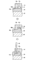
- FIG. 6 shows an initial state in which the imprint operation is performed by pressing the mold 10 against the surface of the resist 30 applied to the base material 20.
- the uneven pattern of the mold 10 is in contact with the resist 30.
- the concave portion 15a in the concave-convex pattern on the lower surface of the mold 10 is blocked from the outside, and the condensable gas 140a in the concave portion 15a is sealed.
- the convex portion 15b of the concave / convex pattern on the lower surface of the mold 10 is pushed into the softened resist 30, and the resist 30 enters the concave portion 15a.
- the condensable gas 140a that is sealed in the recess 15a is compressed, and the pressure inside the recess 15a increases.
- the resist 30 in the recess 15a rises in the space and compresses the condensable gas 140a inside.
- the pressure in the space A in which the condensable gas 140a is confined increases in proportion to the decrease in volume. Since the condensable gas 140a is selected as a gas that becomes liquid at the desired compression at the temperature of the above-mentioned working part, a part of the condensable gas 140a in the recess 15a is liquefied by the compression of the condensable gas 140a.
- the pressure of the recess 15a is kept below the vapor pressure of the gas.
- the pressure applied to the space A of the recess 15a is larger than the vapor pressure of the gas, the liquefaction of the gas occurs continuously.
- all the gas is liquefied, and the resist 30 that has entered the recess 15a is, for example, As shown in the lower side of FIG. 6, almost all the space A of the recess 15a is filled.
- the space A in the concave portion 15a of the mold 10 can be completely filled with the resist 30 by the liquefaction of the condensable gas 140a. Therefore, the problem that the concavo-convex pattern of the mold 10 cannot be accurately transferred due to the compressed gas remaining in the space A in the recess 15a as in the conventional nanoimprint can be solved.
- Pattern formation at the time of semiconductor manufacture As an example of using the imprint method according to this embodiment and this modification, after forming a wiring groove or a via hole using the imprint method, a metal wiring and a plug are formed by a dual damascene method. It can be used for manufacturing a semiconductor device. By using this imprint method instead of the conventional lithography technique, the cost can be reduced.
- Pattern formation at the time of manufacturing a recording medium can be used when a desired pattern is formed on a medium when manufacturing a recording medium such as an HDD or a CD.
- a desired pattern is formed on a medium when manufacturing a recording medium such as an HDD or a CD.
- HDD hard disk drive
- it can be used for a discrete track medium in which data tracks are magnetically separated.
- Discrete track media are intended to improve signal quality by removing (grooving) a portion of magnetic material that is not necessary for recording.
- the imprint method according to this embodiment and this modification can be used. After the grooves are processed, the data tracks are magnetically separated by filling the grooves with a nonmagnetic material.
- the transparent conductive film (antireflection film) formed by applying an In 2 O 3 —SnO 2 -based sol on the translucent substrate 1 is applied to the present embodiment and A pattern is formed using the pattern forming apparatus according to this modification.
- a micro pyramid structure is formed on the surface of the antireflection film.
- the Ni electroforming mold as a stamper (corresponding to the mold) has a plurality of convex portions having a quadrangular pyramid shape, and the Ni electroforming mold is pressed against the surface of the transparent conductive film by pressing the plurality of convex portions of the Ni electroforming mold
- the transparent conductive film is pressure-bonded for 10 minutes while being heated to form an uneven portion on the transparent conductive film.
- Pattern formation at the time of manufacturing a lens array When manufacturing a microlens array with a small coupling loss, which is used for optical coupling between optical fibers, the imprint method using the pattern forming apparatus according to this embodiment and this modification is also used.
- the lens array pattern can be transferred.
- the microlens array may be plastic or glass.
- Pattern formation on the antireflection film of the light emitting diode In addition, when forming the pattern on the antireflection film of the light emitting diode, an imprint method using the pattern forming apparatus according to this embodiment and this modification can be used.
- the nanoimprint method using the pattern forming apparatus includes magnetic fields such as a semiconductor integrated circuit, a flat screen, a micro electro mechanical system (MEMS), a sensor element, an optical disk, and a high-density memory disk.
- Optical components such as recording media, diffraction grating relief holograms, nanodevices, optical devices, flat panel display production, thin film transistors for liquid crystal displays, organic transistors, color filters, overcoat layers, pillar materials , Used for pattern formation used in the manufacture of liquid crystal alignment rib materials, microlens arrays, immunoassay chips, DNA separation chips, microreactors, nanobiodevices, optical waveguides, optical filters, photonic crystal devices, etc. Door can be.
- the present invention is not limited to the above fields and can be applied to various fields.
- the molding material and the molding material can be peeled reliably and quickly, and the throughput at the time of pattern formation can be improved.
- the optical imprint technique is used, but the present invention is not limited to such an example.
- the imprint method according to the present invention may use a thermal imprint technique.
- a resin as a molding material is cured by heating to transfer a reversal pattern of a mold as a molding material to the molding material.
- the material to be molded is formed by applying a thermoplastic resin to a base material.
- the mold as the molding material may not be quartz, and for example, a pattern may be formed on a silicon substrate or a silicon oxide layer on the silicon substrate.
- the mold is cooled to a glass transition temperature or lower, and the mold and the thermoplastic resin are pulled apart.
- heat is applied when the resin is deformed, and cooling is performed when the resin is embossed and hardened.
- the peeling process for peeling the molding material from the molding material includes a separation process for separating the molding material in a direction opposite to the pressing direction of the molding material, and a molding material. And a pressing step of pressing in the same direction as the pressing direction of the molding material.
- the material to be molded according to the present invention may be a resin or glass.
- the molding material according to the present invention may be of a type that transfers in accordance with the wafer size, or may be one in which the wafer is divided into a plurality of units and transferred for each unit as described above.
Landscapes
- Engineering & Computer Science (AREA)
- Nanotechnology (AREA)
- Chemical & Material Sciences (AREA)
- Physics & Mathematics (AREA)
- Mechanical Engineering (AREA)
- General Physics & Mathematics (AREA)
- Crystallography & Structural Chemistry (AREA)
- Condensed Matter Physics & Semiconductors (AREA)
- Mathematical Physics (AREA)
- Theoretical Computer Science (AREA)
- Manufacturing & Machinery (AREA)
- Shaping Of Tube Ends By Bending Or Straightening (AREA)
- Moulds For Moulding Plastics Or The Like (AREA)
- Exposure Of Semiconductors, Excluding Electron Or Ion Beam Exposure (AREA)
Abstract
【課題】パターン形成において成形材と被成形材とを迅速に剥離させることが可能な、新規かつ改良されたインプリント方法を提供する。 【解決手段】所望のパターンが形成されたモールド10をレジスト30に圧着させることによりモールド10の反転パターンをレジスト30に転写する転写工程と、加熱または光の照射によりレジスト30を硬化させる硬化工程と、硬化工程によりレジスト30が硬化した後、モールド10とレジスト30とを剥離する剥離工程と、を含み、剥離工程は、モールド10をレジスト30の圧着方向と反対方向に引き離す引離し工程と、レジスト30をモールド10の圧着方向と同方向に押し付ける押付け工程と、を含むことを特徴とするインプリント方法を提供する。
Description
本発明は、所望のパターンが形成された成形材を被成形材に圧着させることにより、成形材の反転パターンを被成形材に転写するインプリント方法に関する。
半導体製造では、リソグラフィー技術を用いて基材上に所望のパターンを形成することが一般的に行われている。短波長のレーザや電子線を用いたリソグラフィー技術により更なる微細加工を実現しているものもある。
しかし、リソグラフィー技術は、転写、露光、現像という多工程を要する。また、紫外等の短波長のレーザは購入価格及び維持費用が高い上、装置が大型化したり、露光に時間がかかったりして高コストになるという問題がある。
これに対して、インプリント方法により基材上に所望のパターンを形成することも提案されている(例えば、特許文献1、2を参照)。これによれば、リソグラフィー技術よりも工程数が少なくなる。また、レーザが不要であり、かつ大気中でパターン形成が可能となるため、装置構成をシンプルにできる。したがって、インプリント技術は、価格面や装置の維持管理面でリソグラフィー技術より有利である。
しかしながら、インプリント方法は、成形材を被成形材から離すために多くの時間を要していた。成形材を被成形材に押し当てて成形材に形成された凹凸パターンを被成形材に転写し、被成形材を硬化した後、成形材を上昇させて被成形材から剥離させる際、成形材が被成形材から簡単には剥がれないためである。これにより、現状では、1時間に処理できるウエハの枚数は4枚程度と少なく、スループットに問題を有していた。
上記課題に対して、本発明の目的とするところは、パターン形成において成形材と被成形材とを迅速に剥離させることが可能な、新規かつ改良されたインプリント方法を提供することにある。
上記課題を解決するために、本発明のある観点によれば、所望のパターンが形成された成形材を被成形材に圧着させることにより前記成形材の反転パターンを前記被成形材に転写する転写工程と、加熱または光の照射により前記被成形材を硬化させる硬化工程と、前記硬化工程により前記被成形材が硬化した後、前記成形材と前記被成形材とを剥離する剥離工程と、を含み、前記剥離工程は、前記成形材を前記被成形材の圧着方向と反対方向に引き離す引離し工程と、前記被成形材を前記成形材の圧着方向と同方向に押し付ける押付け工程と、を含むことを特徴とするインプリント方法が提供される。
かかる構成によれば、押付け工程と引離し工程とを含んだ剥離工程が実行される。具体的には、押付け工程にて被成形材を圧着方向と同方向に押し付けながら、引離し工程にて成形材を被成形材の圧着方向と反対方向に引き離す。このとき、前記引離し工程と前記剥離工程とは連動して行われてもよいし、同時に行われてもよい。
単に成形材を被成形材の圧着方向と反対方向に引き離すだけの剥離方法では剥がすまでに多くの時間を要していたのに対して、これによれば、成形材と被成形材とを確実かつ迅速に剥離させることができる。この結果、パターン形成時のスループットを向上させることができる。
前記押付け工程は、ピンを前記成形材に設けられた貫通穴に通して前記被成形材に当接することにより、前記被成形材を前記成形材の圧着方向と同方向に押し付けてもよい。
前記ピン及び前記成形材の貫通穴は、それぞれ複数設けられ、前記複数の貫通穴を通り抜けて前記被成形材に当接する前記複数のピンの配置は、前記成形材に形成されたパターン密度に応じて適正化されてもよい。
前記ピン及び前記成形材の貫通穴は、それぞれ複数設けられ、前記複数の貫通穴を通り抜けて前記被成形材に当接する前記複数のピンの配置は、等間隔であってもよい。
前記複数のピンの長さは、前記成形材の厚みの5倍以上に形成されてもよい。
前記インプリント方法は、半導体のパターン形成、記録媒体のパターン形成、太陽電池のパターン形成、レンズアレイのパターン形成、フォトニック結晶デバイスの製造、及び発光ダイオードの反射防止膜のパターン形成の少なくともいずれかの用途に用いられてもよい。
前記転写工程は、前記成形材の凹部に前記被成形材が入り込むときの温度及び凹部内の圧力で凝縮する気体の雰囲気内で行われてもよい。
以上説明したように、本発明によれば、パターン形成において成形材と被成形材とを迅速に剥離させることが可能なインプリント方法を提供することができる。
以下に添付図面を参照しながら、本発明の実施形態について詳細に説明する。なお、本明細書及び図面において、実質的に同一の機能構成を有する構成要素については、同一の符号を付することにより重複説明を省略する。
[ナノインプリントの工程]
まず、本発明の第1実施形態に係るナノインプリントの工程について図1を参照しながら説明する。なお、ナノインプリントとは、被成形材にモールド(型)と呼ばれる成形材を押しつけることにより、被成形材にナノメートルオーダのパターンを転写する微細加工技術である。ナノインプリント技術は、例えば以下に説明する半導体製造時のパターン形成に、従来使用されていたリソグラフィー技術に替えて使用される。
まず、本発明の第1実施形態に係るナノインプリントの工程について図1を参照しながら説明する。なお、ナノインプリントとは、被成形材にモールド(型)と呼ばれる成形材を押しつけることにより、被成形材にナノメートルオーダのパターンを転写する微細加工技術である。ナノインプリント技術は、例えば以下に説明する半導体製造時のパターン形成に、従来使用されていたリソグラフィー技術に替えて使用される。
ナノインプリントは、位置合わせ工程、圧着工程、転写工程、離型工程、ピン退避工程、モールド及びピン移動工程、を一連の工程として被成形材へのパターン転写を実行する。
以下の説明では、本実施形態に係る成形材としてモールド10が使用される。モールド10は、紫外線(UV)を透過する石英の基材であって、表面に所望の凹凸パターンが形成されたものである。図2には、図1の最上図に示したモールド10の1-1断面が示されている。モールド10は、断面が正方形であって等間隔に9つの貫通穴10aが設けられている。
また、本実施形態に係る被成形材としては、シリコン基板等の基材20が使用される。基材20には樹脂が塗布されている。以下では、基材20上に形成された前記樹脂部分をレジスト30とも称呼する。レジスト30には、紫外線を照射すると硬化する低粘性の光硬化樹脂が利用されてもよい。
(位置合わせ工程)
まず、図1の第1工程の<位置合わせ工程>が実行される。この工程ではたとえば光学的な方法等の周知の方法でモールド10と基材20のX-Y方向(基材20の面方向)の位置合わせを行う。
まず、図1の第1工程の<位置合わせ工程>が実行される。この工程ではたとえば光学的な方法等の周知の方法でモールド10と基材20のX-Y方向(基材20の面方向)の位置合わせを行う。
(圧着工程)
次に、図1の第2工程の<圧着工程>が実行される。圧着工程では、モールド10を基材20に向けて降下させ、そのモールド10をレジスト30に圧着させる。これにより、レジスト30がモールド10の凹部に入り込む。このようにして、モールド10の凹凸パターンがレジスト30に形成される。
次に、図1の第2工程の<圧着工程>が実行される。圧着工程では、モールド10を基材20に向けて降下させ、そのモールド10をレジスト30に圧着させる。これにより、レジスト30がモールド10の凹部に入り込む。このようにして、モールド10の凹凸パターンがレジスト30に形成される。
(転写工程)
次に、図1の第3工程の<転写工程>が実行される。転写工程では、UV光源40から紫外線を照射し、基材20上のレジスト30を硬化させる。これにより、モールド10の反転パターンをレジスト30に転写する。レジスト30に室温で瞬時に硬化する光硬化樹脂を使用するため、加熱、加圧によるパターン変形を生じず、高速プロセスが可能である。
次に、図1の第3工程の<転写工程>が実行される。転写工程では、UV光源40から紫外線を照射し、基材20上のレジスト30を硬化させる。これにより、モールド10の反転パターンをレジスト30に転写する。レジスト30に室温で瞬時に硬化する光硬化樹脂を使用するため、加熱、加圧によるパターン変形を生じず、高速プロセスが可能である。
(離型工程)
次に、図1の第4工程の<離型工程(剥離工程)>が実行される。離型工程では、転写工程で硬化したレジスト30からモールド10を剥離する。離型工程は、モールド10をレジスト30の圧着方向(ここではモールド降下方向)と反対方向に引き離す動作(引離し工程)と、レジスト30をモールド10の圧着方向と同方向に押し付ける動作(押付け工程)と、を含んでいる。
次に、図1の第4工程の<離型工程(剥離工程)>が実行される。離型工程では、転写工程で硬化したレジスト30からモールド10を剥離する。離型工程は、モールド10をレジスト30の圧着方向(ここではモールド降下方向)と反対方向に引き離す動作(引離し工程)と、レジスト30をモールド10の圧着方向と同方向に押し付ける動作(押付け工程)と、を含んでいる。
引離し工程では、前述の通りモールド10をレジスト30の圧着方向と反対方向に上昇させることによりモールド10をレジスト30から剥がす。しかしながら、この動作だけでは、モールド10を上昇させる際、モールド10が簡単には剥がれない。これが、ナノインプリント方法によるパターン形成の処理速度を遅くする主な要因となっていた。
そこで、本実施形態に係るナノインプリント方法では、引離し工程とともに押付け工程が設けられている。これは、複数のピン50をモールド10に設けられた貫通穴10aに通してレジスト30に押し当てることにより実行される。
ピン50を降下させるタイミングは、レジスト30が硬化した後でもよく、UV光を照射中でもよい。ただし、ピン50をレジスト30に当接させるタイミングは、レジスト30が硬化した後でなければならない。このように、引離し工程と押付け工程とは、レジスト30が硬化した後に連動して行われる。引離し工程と押付け工程とはほぼ同時に行われるようにしてもよい。
(ピン退避工程)
次に、図1の第5工程の<ピン退避工程>が実行される。ピン退避工程では、モールド10がレジスト30から完全に剥離したら、モールド10の上方までピン50を上昇させ、モールド10の移動時にピン50が邪魔にならないようにピン50を退避させる。
次に、図1の第5工程の<ピン退避工程>が実行される。ピン退避工程では、モールド10がレジスト30から完全に剥離したら、モールド10の上方までピン50を上昇させ、モールド10の移動時にピン50が邪魔にならないようにピン50を退避させる。
(モールド及びピン移動工程)
上記位置合わせ工程からピン退避工程までの一連の工程により、ナノインプリントによる1ユニットのパターン形成が完了する。次に、図1の最終工程の<モールド及びピン移動工程>では、基材20上の他のレジスト30部分にパターンを形成するために、モールド10及びピン50を所定位置までスライド移動させる。
上記位置合わせ工程からピン退避工程までの一連の工程により、ナノインプリントによる1ユニットのパターン形成が完了する。次に、図1の最終工程の<モールド及びピン移動工程>では、基材20上の他のレジスト30部分にパターンを形成するために、モールド10及びピン50を所定位置までスライド移動させる。
以上、位置合わせ工程からモールド及びピン移動工程までの一連の工程を基材全体にパターンを転写し終わるまで繰り返す。これにより、基材全体に所望のパターンが形成される。
以上に説明したように、本実施形態に係るナノインプリント方法を用いたパターン形成によれば、ピン50によりレジスト30を圧着方向と同方向に押し付けながら、モールド10をレジスト30の圧着方向と反対方向に引き離す。これにより、単にモールド10をレジスト30の圧着方向と反対方向に引き離すだけでは剥がれにくかったレジスト30とモールド10とを確実かつ迅速に剥離させることができる。これにより、パターン形成時のスループットを向上させることができる。
[ピンの構成]
次に、以上に説明した工程のうち、押付け工程で用いられるピン50の特徴及び配置について説明する。
次に、以上に説明した工程のうち、押付け工程で用いられるピン50の特徴及び配置について説明する。
(ピンの特徴)
ピン50の素材としては、アルミニウムやステンレスが挙げられる。ただし、ピン50の先端は、レジスト30を傷つけないように、例えばべスペル(登録商標)等の耐摩擦性に優れた全芳香族ポリイミド樹脂やフッ素入り樹脂等で形成される。
ピン50の素材としては、アルミニウムやステンレスが挙げられる。ただし、ピン50の先端は、レジスト30を傷つけないように、例えばべスペル(登録商標)等の耐摩擦性に優れた全芳香族ポリイミド樹脂やフッ素入り樹脂等で形成される。
ピン50の直径は、形成するパターンの微細度に応じてミクロンオーダからミリオーダまでの大きさに形成される。ピン50の長さは、モールド10の厚みに対して5倍以上、10倍以下に形成される。
(ピンの配置)
次に、モールド10のパターン密度が不均一の場合のピンの配置、モールド10のパターン密度が均一の場合のピンの配置について図2及び図3を参照しながら順に説明する。
次に、モールド10のパターン密度が不均一の場合のピンの配置、モールド10のパターン密度が均一の場合のピンの配置について図2及び図3を参照しながら順に説明する。
モールド10のパターン密度が不均一の場合、貫通穴10aを通り抜けてレジスト30に当接するピン50の配置は、モールド10に形成されたパターン密度に応じて適正化される。
例えば、図3の上図、中央図、下図には、図2の上側に示したモールド10の2-2断面、3-3断面、4-4断面が示されている。図3の上図では、モールド10のパターン密度は、図面左側が密、右側が疎である。したがって、図2の上側の2-2切断線上の貫通穴10aのうち、左側2つの貫通穴10aのみからピン50を通し、図3の上図に示したように、左側のピン50及び中央のピン50でレジスト30を押圧する。このようにして、パターン密度が高い左側部分はパターン密度が低い右側部分よりレジスト30を押し付けるピン50の配置を密にする。
図3の中央図では、モールド10のパターン密度は、図面左側及び右側のいずれも密である。したがって、図2の上側の3-3切断線上の貫通穴10aのすべてからピン50を通し、図3の中央図に示したように、3本のピン50でレジスト30の全体を均等に押圧する。このようにして、パターン密度が均等に高い場合、レジスト30全体をピン50で均等に押し付ける。
図3の下図では、モールド10のパターン密度は、図面左側が疎、右側が密である。したがって、図2の上側の4-4切断線上の貫通穴10aのうち、右側2つの貫通穴10aのみからピン50を通し、図3の下図に示したように、右側のピン50及び中央のピン50でレジスト30を押圧する。このようにして、パターン密度が高い右側部分はパターン密度が低い左側部分よりレジスト30を押し付けるピン50の配置を密にする。
以上に説明したようにして、モールド10のパターン密度が不均一の場合、複数の貫通穴10aを通り抜けてレジスト30に当接する複数のピン50の配置をモールド10に形成されたパターン密度に応じて適正化することにより、確実及び迅速にモールド10とレジスト30とを剥離することができる。
モールド10のパターン密度が均一の場合、図2の下側に示したように、複数の貫通穴10aを通り抜けてレジスト30に当接する複数のピン50の配置を等間隔にする。図2の下側では、モールド10の4つの角部近傍の貫通穴10aから4つのピン50が貫通し、等間隔にレジスト30に当接する。しかしながら、これに限られず、例えば、モールド10に設けられた9つの貫通穴10aのすべてから9つのピン50をレジスト30に押しつけるようにしてもよい。
[パターン形成装置]
次に、上述した本実施形態に係るナノインプリント方法を実行するパターン形成装置について、図4を参照しながら説明する。図4は、本実施形態に係るパターン形成装置の全体構成を示した縦断面図である。
次に、上述した本実施形態に係るナノインプリント方法を実行するパターン形成装置について、図4を参照しながら説明する。図4は、本実施形態に係るパターン形成装置の全体構成を示した縦断面図である。
パターン形成装置100は、内部でナノインプリント方法が実行される処理容器105を有する。処理容器105には、定盤110上に摺動ステージ115が設けられている。摺動ステージ115は、水平面内を自在に摺動する。これにより、摺動ステージ115上の基材20(及びレジスト30)は水平移動するようになっている。
処理容器105内にはモールド10を昇降させ、モールド10下面に形成された凹凸パターンをその下方に位置するレジスト30に押しつけるための昇降ステージ120が設置されている。摺動ステージ115を摺動するにより基材20が移動して所定位置で停止したとき、昇降ステージ120のモールド押圧機構(成形材押圧機構)120aが作動し、モールド10が降下する。降下によりモールド10がレジスト30に密着すると、モールド10下面の凹凸パターンがレジスト30に押しつけられ、軟化しているレジスト30内にモールド10の凹凸パターンが形成される。
その後、処理容器105の天井面上に設置されたUV光源40からサファイア窓を通して紫外光が照射され、レジスト30を硬化させる。紫外光によりレジスト30を硬化中又は硬化後、エアーシリンダ130に接続されたエアー供給源125からエアーシリンダ130内に所定量のエアーを流入する。これにより、エアーシリンダ130に連結されたピン50がレジスト30に向けて降下する。ただし、レジスト30が完全に硬化するまでピン50はレジスト30に当接させない。
レジスト30が光硬化後、更なるエアー流入によりピン50をレジスト30に当接させながら、モールド押圧機構120aによりモールド10を上昇させる。これにより、モールド10をスムーズにレジスト30から離す。
モールド押圧機構120aによりモールド10を完全に上昇させる。さらに、エアーシリンダ130内から所定量のエアーを流出することにより、エアーシリンダ130に連結されたピン50を完全に退避させる。その状態で摺動ステージ115を移動させることによって基材20を水平方向に移動し、モールド10の下面に次にインプリントを行いたいレジスト30を位置させ、以下同様の作業を繰り返す。このようにして、パターン形成装置100により、レジスト30全体に図1に示したナノインプリントによるパターンが形成される。
[パターン形成装置の変形例]
次に、本実施形態の変形例に係るパターン形成装置について、図5を参照しながら説明する。図5は、本変形例に係るパターン形成装置の全体構成を示した縦断面図である。
次に、本実施形態の変形例に係るパターン形成装置について、図5を参照しながら説明する。図5は、本変形例に係るパターン形成装置の全体構成を示した縦断面図である。
本変形例に係るパターン形成装置には、本実施形態に係るパターン形成装置の各構成に加え、排気装置135及び凝縮性ガス供給源140がさらに備えられている。本変形例では、排気装置135を用いて処理容器105内の大気を抜き、その後、処理容器105内に凝縮性ガス供給源140から所定成分の凝縮性ガスを供給する。その際には処理容器105内の圧力が予め設定した所定の圧力になるように凝縮性ガスを供給する。このとき、処理容器105内の温度は例えば常温であってもよい。
なお、ここでいう「凝縮性ガス」とは、後述するように、インプリント作業時にモールド10の凹部にレジスト30が侵入してモールド10の凹部の内部に閉じこめられた気体を圧縮するとき、その圧力によって凝縮することができる気体をいう。
凝縮性ガスとしては種々のものを選択することができる。例えば室温(23℃)での蒸気圧が0.1056MPaのトリクロロフルオロメタンを凝縮性ガスとして用いてもよい。このような気体であれば蒸気圧よりも少し低圧の、例えば0.1MPa程度になるように所定量を処理容器105内に供給する。このような凝縮性のある気体雰囲気を構成する物質の沸点は、処理容器105の圧力が1気圧程度であれば15℃~30℃程度の常温に近い温度であることが好ましい。但し、凝縮性ガスの種類によっては、処理容器105内の圧力設定との関係で適宜変更される。
このような凝縮性ガスの雰囲気中でインプリントによるパターン形成を行った場合の作用及び効果について説明する。図6の上側には、モールド10を基材20に塗布したレジスト30の表面に押しつけることによりインプリント作業を行う最初の状態が示されている。ここでは、モールド10の凹凸パターンがレジスト30に当接している。この時、モールド10下面の凹凸パターンのうちの凹部15aが外界から遮断され、凹部15a内の凝縮性ガス140aは密封状態となる。
その後、さらにモールド10が降下すると、軟化しているレジスト30内にモールド10下面の凹凸パターンのうちの凸部15bが押し込まれ、レジスト30が凹部15a内に入り込む。それにより、凹部15a内にて密封状態となっている凝縮性ガス140aは圧縮され、凹部15a内部の圧力は上昇する。
このようにして、例えば図6の中央に示すように、凹部15a内のレジスト30はその空間内で上昇し、内部の凝縮性ガス140aを圧縮する。この圧縮により、凝縮性ガス140aが閉じ込められた空間Aの圧力は、体積減少に比例して上昇する。凝縮性ガス140aは、前述の作業部分の温度において所望の圧縮時に液体になるガスが選択されているので、凝縮性ガス140aの圧縮によって凹部15a内の凝縮性ガス140aの一部が液化する。
凹部15aの空間A内の凝縮性ガス140aの液化によって、凹部15aの圧力がガスの蒸気圧以下に保たれる。凹部15aの空間Aにかかる圧力が、ガスの蒸気圧よりも大きい場合にはガスの液化が連続して起こり、ついには全てのガスが液化し、凹部15a内に侵入してきたレジスト30は、例えば図6の下側に示すように、ほとんどその凹部15aの空間Aを全て充填する状態となる。
以上に説明したように、変形例に係るパターン形成装置を用いたナノインプリント方法によれば、凝縮性ガス140aの液化によりモールド10の凹部15aの空間Aをレジスト30で完全に充填することができる。よって、従来のナノインプリントのように、凹部15a内の空間Aに圧縮された気体が残ることによりモールド10の凹凸パターンが正確に転写できないという問題を解決することができる。
[ナノインプリントによるパターン形成の利用例]
最後に、本実施形態に係るパターン形成装置及び本変形例に係るパターン形成装置を用いたナノインプリント方法を用いる用途について、いくつかの具体的利用例を述べる。
最後に、本実施形態に係るパターン形成装置及び本変形例に係るパターン形成装置を用いたナノインプリント方法を用いる用途について、いくつかの具体的利用例を述べる。
1.半導体製造時のパターン形成
本実施形態及び本変形例に係るインプリント方法の利用例としては、インプリント法を用いて配線溝又はヴィアホールを形成した後、デュアルダマシン法により金属配線及びプラグを形成する半導体装置の製造に利用することができる。従来のリソグラフィー技術に替えてこのインプリント方法を用いることにより、コスト安を図ることができる。
本実施形態及び本変形例に係るインプリント方法の利用例としては、インプリント法を用いて配線溝又はヴィアホールを形成した後、デュアルダマシン法により金属配線及びプラグを形成する半導体装置の製造に利用することができる。従来のリソグラフィー技術に替えてこのインプリント方法を用いることにより、コスト安を図ることができる。
2.記録媒体製造時のパターン形成
また、HDD、CD等の記録媒体製造時に媒体上に所望のパターンを形成する場合に利用することができる。例えば、ハードディスクドライブ(HDD)の記録密度を高めるために、データトラックを磁気的に分離して形成するディスクリートトラックメディアに利用することができる。ディスクリートトラックメディアは、記録に不要な部分の磁性材料を除去(溝加工)して信号品質を改善しようとするものである。記録媒体上に所望の溝パターンを形成する際、本実施形態及び本変形例に係るインプリント方法を用いることができる。溝加工した後にその溝を非磁性材料で充填することにより、データトラックを磁気的に分離する。
また、HDD、CD等の記録媒体製造時に媒体上に所望のパターンを形成する場合に利用することができる。例えば、ハードディスクドライブ(HDD)の記録密度を高めるために、データトラックを磁気的に分離して形成するディスクリートトラックメディアに利用することができる。ディスクリートトラックメディアは、記録に不要な部分の磁性材料を除去(溝加工)して信号品質を改善しようとするものである。記録媒体上に所望の溝パターンを形成する際、本実施形態及び本変形例に係るインプリント方法を用いることができる。溝加工した後にその溝を非磁性材料で充填することにより、データトラックを磁気的に分離する。
3.太陽電池製造時のパターン形成
太陽電池製造プロセスでは、例えば透光性基板1上にIn2O3-SnO2系ゾルを塗布して形成した透明導電膜(反射防止膜)に、本実施形態及び本変形例に係るパターン形成装置を用いてパターンを形成する。ここでは、反射防止膜の表面にミクロなピラミッド構造を形成する。スタンパ(モールドに対応)としてのNi電鋳金型は、四角錐形状の複数の凸部を有し、Ni電鋳金型の複数の凸部を透明導電膜の表面に押し付けて、Ni電鋳金型と透明導電膜を加熱しながら10分間圧着し、透明導電膜に凹凸部を形成する。
太陽電池製造プロセスでは、例えば透光性基板1上にIn2O3-SnO2系ゾルを塗布して形成した透明導電膜(反射防止膜)に、本実施形態及び本変形例に係るパターン形成装置を用いてパターンを形成する。ここでは、反射防止膜の表面にミクロなピラミッド構造を形成する。スタンパ(モールドに対応)としてのNi電鋳金型は、四角錐形状の複数の凸部を有し、Ni電鋳金型の複数の凸部を透明導電膜の表面に押し付けて、Ni電鋳金型と透明導電膜を加熱しながら10分間圧着し、透明導電膜に凹凸部を形成する。
このように反射防止膜の表面にピラミッド状の凹凸を形成することにより、入射した光は、反射防止膜の表面に形成されたピラミッド構造により透過及び反射を繰り返し、その結果、フラットな表面よりも多くの光を太陽電池の内部に導くことができる。
4.レンズアレイ製造時のパターン形成
光ファイバ間の光結合等に用いる、結合損失の少ないマイクロレンズアレイを製造する際にも、本実施形態及び本変形例に係るパターン形成装置を用いたインプリント方法によってレンズアレイパターンを転写することができる。なお、マイクロレンズアレイは、プラスチックでもよく、ガラスでもよい。
光ファイバ間の光結合等に用いる、結合損失の少ないマイクロレンズアレイを製造する際にも、本実施形態及び本変形例に係るパターン形成装置を用いたインプリント方法によってレンズアレイパターンを転写することができる。なお、マイクロレンズアレイは、プラスチックでもよく、ガラスでもよい。
5.発光ダイオードの反射防止膜上のパターン形成
その他、発光ダイオードの反射防止膜上のパターンを形成する際にも、本実施形態及び本変形例に係るパターン形成装置を用いたインプリント方法が利用できる。
その他、発光ダイオードの反射防止膜上のパターンを形成する際にも、本実施形態及び本変形例に係るパターン形成装置を用いたインプリント方法が利用できる。
このように、本実施形態及び本変形例に係るパターン形成装置を用いたナノインプリント方法は、半導体集積回路、フラットスクリーン、マイクロ電気機械システム(MEMS)、センサ素子、光ディスク、高密度メモリーデイスク等の磁気記録媒体、回折格子ヤレリーフホログラム等の光学部品、ナノデバイス、光学デバイス、フラットパネルディスプレイ製作のための光学フィルムや偏光素子、液晶ディスプレイの薄膜トランジタ、有機トランジスタ、カラーフィルター、オーバーコート層、柱材、液晶配向用のリブ材、マイクロレンズアレイ、免疫分析チップ、DNA分離チップ、マイクロリアクター、ナノバイオデバイス、光導波路、光学フィルター、フォトニック結晶デバイスの製造等の作製に用いられるパターン形成に用いることができる。
そして、いずれのパターン形成においても本実施形態及び本変形例のナノインプリント方法によれば、モールドを一度作製すれば、ナノ構造等の微細構造が簡単に繰り返して成型できるため経済的であるとともに、有害な廃棄・排出物が少ないナノ加工技術である。よって、上記分野以外に限られず、さまざまな分野に応用することができる。
以上、上記実施形態及び上記変形例に係るインプリント方法によれば、成形材と被成形材の剥離を確実かつ迅速に行うことができ、パターン形成時のスループットを向上させることができる。
以上、添付図面を参照しながら本発明の好適な実施形態について詳細に説明したが、本発明はかかる例に限定されない。本発明の属する技術の分野における通常の知識を有する者であれば、請求の範囲に記載された技術的思想の範疇内において、各種の変更例または修正例に想到し得ることは明らかであり、これらについても、当然に本発明の技術的範囲に属するものと了解される。
例えば、本実施形態及び本変形例に係るインプリント方法では、光インプリント技術を利用したが、本発明はかかる例に限定されない。例えば、本発明に係るインプリント方法は、熱インプリント技術を利用してもよい。
熱インプリントでは、加熱により被成形材としての樹脂を硬化させることにより、成形材としてのモールドの反転パターンを被成形材に転写する。被成形材は、熱可塑性樹脂を基材に塗布することにより形成される。成形材としてのモールドは、石英でなくてもよく、例えばシリコン基板やシリコン基板上の酸化シリコン層にパターンを形成してもよい。モールドを熱可塑性樹脂に圧着後、ガラス転移温度以下に冷却し、モールドと熱可塑性樹脂を引き離す。このように、熱インプリントでは、樹脂を変形させるときに熱を加えて、型押しして固めるときに冷却する。
熱インプリントの場合にも、被成形材の硬化後、被成形材から成形材を剥離させる剥離工程は、成形材を被成形材の圧着方向と反対方向に引き離す引離し工程と、被成形材を成形材の圧着方向と同方向に押し付ける押付け工程とを含む。
本発明に係る被成形材は、樹脂であってもよく、ガラスであってもよい。本発明に係る成形材は、ウエハサイズに合わせて転写する型のものであってもよく、上述したようにウエハを複数のユニットに分けて、ユニット毎に転写するものであってもよい。
10 モールド
10a 貫通穴
20 基材
30 レジスト
40 UV光源
50 ピン
100 パターン形成装置
105 処理容器
115 ステージ
120 モールド駆動ステージ
125 エアー供給源
130 エアーシリンダ
135 排気装置
140 凝縮性ガス供給源
10a 貫通穴
20 基材
30 レジスト
40 UV光源
50 ピン
100 パターン形成装置
105 処理容器
115 ステージ
120 モールド駆動ステージ
125 エアー供給源
130 エアーシリンダ
135 排気装置
140 凝縮性ガス供給源
Claims (9)
- 所望のパターンが形成された成形材を被成形材に圧着させることにより、前記成形材の反転パターンを前記被成形材に形成する圧着工程と、
加熱または光の照射により前記被成形材を硬化させることにより、前記成形材の反転パターンを前記被成形材に転写する転写工程と、
前記転写工程により前記被成形材が硬化した後、前記被成形材から前記成形材を剥離させる離型工程と、を含み、
前記離型工程は、
前記成形材を前記被成形材の圧着方向と反対方向に引き離す引離し工程と、
前記被成形材を前記成形材の圧着方向と同方向に押し付ける押付け工程と、
を含むことを特徴とするインプリント方法。 - 前記押付け工程は、ピンを前記成形材に設けられた貫通穴に通して前記被成形材に当接することにより、前記被成形材を前記成形材の圧着方向と同方向に押し付けることを特徴とする請求項1に記載のインプリント方法。
- 前記引離し工程と前記押付け工程とは連動して行われることを特徴とする請求項1に記載のインプリント方法。
- 前記引離し工程と前記押付け工程とは同時に行われることを特徴とする請求項3に記載のインプリント方法。
- 前記ピン及び前記成形材の貫通穴は、それぞれ複数設けられ、
前記複数の貫通穴を通り抜けて前記被成形材に当接する前記複数のピンの配置は、前記成形材に形成されたパターン密度に応じて適正化されることを特徴とする請求項1に記載のインプリント方法。 - 前記ピン及び前記成形材の貫通穴は、それぞれ複数設けられ、
前記複数の貫通穴を通り抜けて前記被成形材に当接する前記複数のピンの配置は、等間隔であることを特徴とする請求項1に記載のインプリント方法。 - 前記複数のピンの長さは、前記成形材の厚みの5倍以上に形成されることを特徴とする請求項1に記載のインプリント方法。
- 前記請求項1に記載のインプリント方法は、
半導体のパターン形成、記録媒体のパターン形成、太陽電池のパターン形成、レンズアレイのパターン形成、フォトニック結晶デバイスの製造、及び発光ダイオードの反射防止膜のパターン形成の少なくともいずれかの用途に用いられることを特徴とするインプリント方法。 - 前記圧着工程は、前記成形材の凹部に前記被成形材が入り込むときの温度及び凹部内の圧力で凝縮する気体の雰囲気内で行われる請求項1に記載のインプリント方法。
Priority Applications (2)
| Application Number | Priority Date | Filing Date | Title |
|---|---|---|---|
| KR1020127023853A KR101409248B1 (ko) | 2010-02-16 | 2011-02-04 | 임프린트 방법 |
| US13/585,970 US9370875B2 (en) | 2010-02-16 | 2012-08-15 | Imprinting method |
Applications Claiming Priority (2)
| Application Number | Priority Date | Filing Date | Title |
|---|---|---|---|
| JP2010-031415 | 2010-02-16 | ||
| JP2010031415A JP5546893B2 (ja) | 2010-02-16 | 2010-02-16 | インプリント方法 |
Related Child Applications (1)
| Application Number | Title | Priority Date | Filing Date |
|---|---|---|---|
| US13/585,970 Continuation US9370875B2 (en) | 2010-02-16 | 2012-08-15 | Imprinting method |
Publications (1)
| Publication Number | Publication Date |
|---|---|
| WO2011102240A1 true WO2011102240A1 (ja) | 2011-08-25 |
Family
ID=44482829
Family Applications (1)
| Application Number | Title | Priority Date | Filing Date |
|---|---|---|---|
| PCT/JP2011/052346 Ceased WO2011102240A1 (ja) | 2010-02-16 | 2011-02-04 | インプリント方法 |
Country Status (4)
| Country | Link |
|---|---|
| US (1) | US9370875B2 (ja) |
| JP (1) | JP5546893B2 (ja) |
| KR (1) | KR101409248B1 (ja) |
| WO (1) | WO2011102240A1 (ja) |
Cited By (3)
| Publication number | Priority date | Publication date | Assignee | Title |
|---|---|---|---|---|
| WO2013035761A1 (en) * | 2011-09-05 | 2013-03-14 | Canon Kabushiki Kaisha | Imprint apparatus, imprint method, and manufacturing method of commodities |
| WO2013042350A1 (en) * | 2011-09-21 | 2013-03-28 | Canon Kabushiki Kaisha | Imprint apparatus and article manufacturing method using same |
| JP2015099899A (ja) * | 2012-11-30 | 2015-05-28 | キヤノン株式会社 | インプリント方法およびインプリント用硬化性組成物 |
Families Citing this family (11)
| Publication number | Priority date | Publication date | Assignee | Title |
|---|---|---|---|---|
| JP6304921B2 (ja) * | 2012-06-05 | 2018-04-04 | キヤノン株式会社 | インプリント方法およびインプリント装置、それを用いた物品の製造方法 |
| US9240565B2 (en) * | 2013-06-06 | 2016-01-19 | Toyo Gosei Co., Ltd. | Composition |
| JP6327948B2 (ja) * | 2013-06-26 | 2018-05-23 | キヤノン株式会社 | 光硬化性組成物、硬化物、これを用いた、膜の製造方法、光学部品の製造方法、回路基板の製造方法、電子部品の製造方法 |
| JP6327947B2 (ja) * | 2013-06-26 | 2018-05-23 | キヤノン株式会社 | 光硬化性組成物、これを用いた、膜の製造方法、光学部品の製造方法、回路基板の製造方法、電子部品の製造方法、硬化物 |
| JP6494185B2 (ja) * | 2013-06-26 | 2019-04-03 | キヤノン株式会社 | インプリント方法および装置 |
| JP6584074B2 (ja) * | 2014-02-26 | 2019-10-02 | キヤノン株式会社 | 光硬化性組成物、硬化物、これを用いた、パターン形状を有する膜の製造方法、光学部品の製造方法、回路基板の製造方法、電子部品の製造方法 |
| JP6704701B2 (ja) * | 2014-12-15 | 2020-06-03 | キヤノン株式会社 | 密着層形成組成物、密着層の製造方法、硬化物パターンの製造方法、光学部品の製造方法、回路基板の製造方法、インプリント用モールドの製造方法、およびデバイス部品 |
| US10418235B2 (en) * | 2015-09-17 | 2019-09-17 | Milara Incorporated | Systems and methods for forming electronic devices from nanomaterials |
| TWI628062B (zh) * | 2016-03-17 | 2018-07-01 | 欣興電子股份有限公司 | 線路板的製作方法與感壓印模 |
| ES2901424T3 (es) | 2017-03-16 | 2022-03-22 | Univ Aix Marseille | Proceso de litografía por nanoimpresión y sustrato con patrón obtenible a partir del mismo |
| EP3422100B1 (en) * | 2017-06-29 | 2019-09-11 | Université d'Aix Marseille | Microtransfer molding process and patterned substrate obtainable therefrom |
Citations (6)
| Publication number | Priority date | Publication date | Assignee | Title |
|---|---|---|---|---|
| JP2002100079A (ja) * | 2000-09-25 | 2002-04-05 | Toshiba Corp | 転写装置及び転写方法 |
| JP2003154549A (ja) * | 2001-11-22 | 2003-05-27 | Mitsubishi Materials Corp | 光ディスク成形用金型装置 |
| JP2007253557A (ja) * | 2006-03-24 | 2007-10-04 | Towa Corp | 成形装置 |
| JP2008221552A (ja) * | 2007-03-12 | 2008-09-25 | Hitachi High-Technologies Corp | 微細構造転写装置、スタンパおよび微細構造の製造方法 |
| JP2008290438A (ja) * | 2007-05-24 | 2008-12-04 | Contrel Technology Co Ltd | 粘着性を有する微細構造を製造する方法 |
| JP2009123318A (ja) * | 2007-10-23 | 2009-06-04 | Tdk Corp | インプリント方法、情報記録媒体製造方法およびインプリントシステム |
Family Cites Families (8)
| Publication number | Priority date | Publication date | Assignee | Title |
|---|---|---|---|---|
| JPS60127544A (ja) * | 1983-12-13 | 1985-07-08 | Matsushita Electric Ind Co Ltd | 光情報担体ディスクの製造方法 |
| US4889311A (en) * | 1988-08-10 | 1989-12-26 | Outboard Marine Corporation | Molding apparatus with improved ejector pin |
| JP3039788B2 (ja) * | 1990-05-18 | 2000-05-08 | ティーディーケイ株式会社 | 光ディスク用基板の製造方法および光ディスク |
| US7641840B2 (en) * | 2002-11-13 | 2010-01-05 | Molecular Imprints, Inc. | Method for expelling gas positioned between a substrate and a mold |
| TW200503167A (en) | 2003-06-20 | 2005-01-16 | Matsushita Electric Industrial Co Ltd | Manufacturing method of semiconductor device |
| JP2007081048A (ja) * | 2005-09-13 | 2007-03-29 | Canon Inc | ナノインプリント用型、装置および方法 |
| KR101313774B1 (ko) * | 2006-12-08 | 2013-10-01 | 엘아이지에이디피 주식회사 | 미세패턴 형성장치 |
| JP5473266B2 (ja) | 2007-08-03 | 2014-04-16 | キヤノン株式会社 | インプリント方法および基板の加工方法、基板の加工方法による半導体デバイスの製造方法 |
-
2010
- 2010-02-16 JP JP2010031415A patent/JP5546893B2/ja not_active Expired - Fee Related
-
2011
- 2011-02-04 KR KR1020127023853A patent/KR101409248B1/ko not_active Expired - Fee Related
- 2011-02-04 WO PCT/JP2011/052346 patent/WO2011102240A1/ja not_active Ceased
-
2012
- 2012-08-15 US US13/585,970 patent/US9370875B2/en not_active Expired - Fee Related
Patent Citations (6)
| Publication number | Priority date | Publication date | Assignee | Title |
|---|---|---|---|---|
| JP2002100079A (ja) * | 2000-09-25 | 2002-04-05 | Toshiba Corp | 転写装置及び転写方法 |
| JP2003154549A (ja) * | 2001-11-22 | 2003-05-27 | Mitsubishi Materials Corp | 光ディスク成形用金型装置 |
| JP2007253557A (ja) * | 2006-03-24 | 2007-10-04 | Towa Corp | 成形装置 |
| JP2008221552A (ja) * | 2007-03-12 | 2008-09-25 | Hitachi High-Technologies Corp | 微細構造転写装置、スタンパおよび微細構造の製造方法 |
| JP2008290438A (ja) * | 2007-05-24 | 2008-12-04 | Contrel Technology Co Ltd | 粘着性を有する微細構造を製造する方法 |
| JP2009123318A (ja) * | 2007-10-23 | 2009-06-04 | Tdk Corp | インプリント方法、情報記録媒体製造方法およびインプリントシステム |
Cited By (4)
| Publication number | Priority date | Publication date | Assignee | Title |
|---|---|---|---|---|
| WO2013035761A1 (en) * | 2011-09-05 | 2013-03-14 | Canon Kabushiki Kaisha | Imprint apparatus, imprint method, and manufacturing method of commodities |
| WO2013042350A1 (en) * | 2011-09-21 | 2013-03-28 | Canon Kabushiki Kaisha | Imprint apparatus and article manufacturing method using same |
| US9694535B2 (en) | 2011-09-21 | 2017-07-04 | Canon Kabushiki Kaisha | Imprint apparatus and article manufacturing method using same |
| JP2015099899A (ja) * | 2012-11-30 | 2015-05-28 | キヤノン株式会社 | インプリント方法およびインプリント用硬化性組成物 |
Also Published As
| Publication number | Publication date |
|---|---|
| US20120306122A1 (en) | 2012-12-06 |
| KR101409248B1 (ko) | 2014-06-18 |
| US9370875B2 (en) | 2016-06-21 |
| JP5546893B2 (ja) | 2014-07-09 |
| KR20120115582A (ko) | 2012-10-18 |
| JP2011171364A (ja) | 2011-09-01 |
Similar Documents
| Publication | Publication Date | Title |
|---|---|---|
| JP5546893B2 (ja) | インプリント方法 | |
| CN101377618B (zh) | 双面压印光刻系统 | |
| CN100584636C (zh) | 纳米印刷模具、其制造方法及纳米印刷装置和方法 | |
| US8113816B2 (en) | Imprint device and imprint method | |
| JP4340086B2 (ja) | ナノプリント用スタンパ、及び微細構造転写方法 | |
| JP4061220B2 (ja) | ナノプリント装置、及び微細構造転写方法 | |
| JP4090374B2 (ja) | ナノプリント装置、及び微細構造転写方法 | |
| US7964135B2 (en) | Method and apparatus for imprinting energy ray-setting resin, and discs and semiconductor devices with imprinted resin layer | |
| JP2004288783A (ja) | ナノプリント装置、及び微細構造転写方法 | |
| JP4886400B2 (ja) | インプリント装置およびインプリント方法 | |
| US20170203471A1 (en) | Imprint template and method for producing the same | |
| JP2013038117A (ja) | 微細パターンを転写するための転写ヘッド及びそれを用いた微細パターンの形成方法 | |
| JP5383110B2 (ja) | インプリント装置 | |
| JP4220282B2 (ja) | ナノプリント装置、及び微細構造転写方法 | |
| JP5155814B2 (ja) | インプリント装置 | |
| JP4944158B2 (ja) | ナノプリント用スタンパ、及び微細構造転写方法 | |
| JP2008078550A (ja) | インプリントモールドおよびその製造方法およびパターン形成方法 | |
| JP5540628B2 (ja) | ナノインプリントパターン形成方法 | |
| JP4244207B2 (ja) | 緩衝層付押圧転写用金型及び押圧転写方法 | |
| JP6699146B2 (ja) | インプリント方法 | |
| JP2007042969A (ja) | ナノインプリントパターン形成用金型およびナノレベルのパターンを有する部材の製造方法 | |
| CN108196425B (zh) | 一种纳米压印衬底固化装置 | |
| JP2007268876A (ja) | パターン転写方法、パターン転写装置及び光ディスク製造方法 |
Legal Events
| Date | Code | Title | Description |
|---|---|---|---|
| 121 | Ep: the epo has been informed by wipo that ep was designated in this application |
Ref document number: 11744528 Country of ref document: EP Kind code of ref document: A1 |
|
| NENP | Non-entry into the national phase |
Ref country code: DE |
|
| ENP | Entry into the national phase |
Ref document number: 20127023853 Country of ref document: KR Kind code of ref document: A |
|
| 122 | Ep: pct application non-entry in european phase |
Ref document number: 11744528 Country of ref document: EP Kind code of ref document: A1 |