WO2011089944A1 - 電気化学デバイス - Google Patents
電気化学デバイス Download PDFInfo
- Publication number
- WO2011089944A1 WO2011089944A1 PCT/JP2011/050243 JP2011050243W WO2011089944A1 WO 2011089944 A1 WO2011089944 A1 WO 2011089944A1 JP 2011050243 W JP2011050243 W JP 2011050243W WO 2011089944 A1 WO2011089944 A1 WO 2011089944A1
- Authority
- WO
- WIPO (PCT)
- Prior art keywords
- heat seal
- terminal
- electrochemical device
- film package
- auxiliary member
- Prior art date
- Legal status (The legal status is an assumption and is not a legal conclusion. Google has not performed a legal analysis and makes no representation as to the accuracy of the status listed.)
- Ceased
Links
Images


Classifications
-
- H—ELECTRICITY
- H01—ELECTRIC ELEMENTS
- H01G—CAPACITORS; CAPACITORS, RECTIFIERS, DETECTORS, SWITCHING DEVICES, LIGHT-SENSITIVE OR TEMPERATURE-SENSITIVE DEVICES OF THE ELECTROLYTIC TYPE
- H01G11/00—Hybrid capacitors, i.e. capacitors having different positive and negative electrodes; Electric double-layer [EDL] capacitors; Processes for the manufacture thereof or of parts thereof
- H01G11/74—Terminals, e.g. extensions of current collectors
-
- H—ELECTRICITY
- H01—ELECTRIC ELEMENTS
- H01G—CAPACITORS; CAPACITORS, RECTIFIERS, DETECTORS, SWITCHING DEVICES, LIGHT-SENSITIVE OR TEMPERATURE-SENSITIVE DEVICES OF THE ELECTROLYTIC TYPE
- H01G11/00—Hybrid capacitors, i.e. capacitors having different positive and negative electrodes; Electric double-layer [EDL] capacitors; Processes for the manufacture thereof or of parts thereof
- H01G11/78—Cases; Housings; Encapsulations; Mountings
- H01G11/80—Gaskets; Sealings
-
- H—ELECTRICITY
- H01—ELECTRIC ELEMENTS
- H01M—PROCESSES OR MEANS, e.g. BATTERIES, FOR THE DIRECT CONVERSION OF CHEMICAL ENERGY INTO ELECTRICAL ENERGY
- H01M50/00—Constructional details or processes of manufacture of the non-active parts of electrochemical cells other than fuel cells, e.g. hybrid cells
- H01M50/10—Primary casings; Jackets or wrappings
- H01M50/172—Arrangements of electric connectors penetrating the casing
- H01M50/174—Arrangements of electric connectors penetrating the casing adapted for the shape of the cells
- H01M50/178—Arrangements of electric connectors penetrating the casing adapted for the shape of the cells for pouch or flexible bag cells
-
- H—ELECTRICITY
- H01—ELECTRIC ELEMENTS
- H01M—PROCESSES OR MEANS, e.g. BATTERIES, FOR THE DIRECT CONVERSION OF CHEMICAL ENERGY INTO ELECTRICAL ENERGY
- H01M50/00—Constructional details or processes of manufacture of the non-active parts of electrochemical cells other than fuel cells, e.g. hybrid cells
- H01M50/50—Current conducting connections for cells or batteries
- H01M50/543—Terminals
- H01M50/547—Terminals characterised by the disposition of the terminals on the cells
- H01M50/55—Terminals characterised by the disposition of the terminals on the cells on the same side of the cell
-
- H—ELECTRICITY
- H01—ELECTRIC ELEMENTS
- H01M—PROCESSES OR MEANS, e.g. BATTERIES, FOR THE DIRECT CONVERSION OF CHEMICAL ENERGY INTO ELECTRICAL ENERGY
- H01M50/00—Constructional details or processes of manufacture of the non-active parts of electrochemical cells other than fuel cells, e.g. hybrid cells
- H01M50/50—Current conducting connections for cells or batteries
- H01M50/543—Terminals
- H01M50/552—Terminals characterised by their shape
- H01M50/553—Terminals adapted for prismatic, pouch or rectangular cells
-
- H—ELECTRICITY
- H01—ELECTRIC ELEMENTS
- H01M—PROCESSES OR MEANS, e.g. BATTERIES, FOR THE DIRECT CONVERSION OF CHEMICAL ENERGY INTO ELECTRICAL ENERGY
- H01M50/00—Constructional details or processes of manufacture of the non-active parts of electrochemical cells other than fuel cells, e.g. hybrid cells
- H01M50/50—Current conducting connections for cells or batteries
- H01M50/543—Terminals
- H01M50/562—Terminals characterised by the material
-
- Y—GENERAL TAGGING OF NEW TECHNOLOGICAL DEVELOPMENTS; GENERAL TAGGING OF CROSS-SECTIONAL TECHNOLOGIES SPANNING OVER SEVERAL SECTIONS OF THE IPC; TECHNICAL SUBJECTS COVERED BY FORMER USPC CROSS-REFERENCE ART COLLECTIONS [XRACs] AND DIGESTS
- Y02—TECHNOLOGIES OR APPLICATIONS FOR MITIGATION OR ADAPTATION AGAINST CLIMATE CHANGE
- Y02E—REDUCTION OF GREENHOUSE GAS [GHG] EMISSIONS, RELATED TO ENERGY GENERATION, TRANSMISSION OR DISTRIBUTION
- Y02E60/00—Enabling technologies; Technologies with a potential or indirect contribution to GHG emissions mitigation
- Y02E60/10—Energy storage using batteries
-
- Y—GENERAL TAGGING OF NEW TECHNOLOGICAL DEVELOPMENTS; GENERAL TAGGING OF CROSS-SECTIONAL TECHNOLOGIES SPANNING OVER SEVERAL SECTIONS OF THE IPC; TECHNICAL SUBJECTS COVERED BY FORMER USPC CROSS-REFERENCE ART COLLECTIONS [XRACs] AND DIGESTS
- Y02—TECHNOLOGIES OR APPLICATIONS FOR MITIGATION OR ADAPTATION AGAINST CLIMATE CHANGE
- Y02E—REDUCTION OF GREENHOUSE GAS [GHG] EMISSIONS, RELATED TO ENERGY GENERATION, TRANSMISSION OR DISTRIBUTION
- Y02E60/00—Enabling technologies; Technologies with a potential or indirect contribution to GHG emissions mitigation
- Y02E60/13—Energy storage using capacitors
Definitions
- the present invention relates to an electrochemical device having a structure in which a power storage element is enclosed in a film package.
- FIG. 1 (A) and FIG. 1 (B) show a conventional electrochemical device RB.
- This electrochemical device RB includes a power storage element 101, a pair of terminals 102 electrically connected to the power storage element 101, and a film package 103 enclosing the power storage element 101.
- the electricity storage element 101 has a substantially rectangular outline in top view, and has a structure in which a collector electrode layer, a polarizable electrode layer, and a separate film are stacked in a predetermined order in the vertical direction. Further, a pair of left and right rectangular terminal connection portions are provided integrally with the current collecting electrode layer at the front edge of the current collecting electrode layer. The left terminal connection portion is used as one polarity, and the right terminal connection portion is used as the other polarity.
- Each terminal 102 has a substantially rectangular outline in top view, the rear end of one terminal 102 is electrically connected to one terminal connection portion of the power storage element 101, and the rear end of the other terminal 102 is connected to the power storage element 101. It is electrically connected to the other terminal connection.
- Each terminal 102 is generally made of a conductive material such as aluminum or platinum.
- the film package 103 has a substantially rectangular top view outline, and is formed using a laminate film LF having a heat-resistant layer LF1, a barrier layer LF2, and a heat seal layer LF3 in this order.
- the heat seal layer LF3 is generally made of a thermoplastic plastic such as polypropylene.
- the terminal lead-out sealing portion 103c is provided continuously with a predetermined width.
- the storage element 101 is enclosed together with the electrolyte, and the front side portion of each terminal 102 is led out of the film package 103 through a terminal lead-out sealing portion 103c.
- the storage element 101 to which each terminal 102 is connected is prepared, and a rectangular laminated film LF having a predetermined size is prepared. Subsequently, the laminate film LF is disposed so that the heat seal layer LF3 faces upward, and the power storage element 101 is placed on the laminate film LF so that the front portion of each terminal 102 protrudes from one film end.
- the laminate film LF is folded in half so that the upper film end is aligned with the lower film end, and the left and right edges are heated to a predetermined width using an appropriate heating device, and heat sealing is performed by the heating.
- the left side sealing portion 103a and the right side sealing portion 103b are formed by heat-sealing and integrating the layers LF3.
- an electrolyte is injected into the inside of the laminated film LF in the form of a bag from the front open portion, and the front edge of the laminated film LF is heated to a predetermined width using an appropriate heating device, and heat sealing is performed by the heating.
- the terminal LF3 sealing portion 103c is formed by heat-sealing and integrating the layers LF3.
- the heating for forming the terminal lead-out sealing portion 103c is performed in a state where a part of each terminal 103 is sandwiched between the upper and lower two heat seal layers LF3, the upper and lower two heat seal layers LF3 are formed by the heating.
- the terminals 102 are integrated, and a part of each terminal 102 is surrounded by the “integrated heat seal material” without a gap (see FIG. 1B).
- the electrochemical device RB can be easily reduced in thickness as compared with other power storage devices by using the film package 103. Therefore, (1) the electrochemical device RB is replaced with electronic components such as a chip capacitor and a chip register. There is a growing demand for reflow soldering to a circuit board together and (2) a demand for encapsulating an electrochemical device RB in an IC card.
- the electrochemical device RB when the electrochemical device RB is encapsulated in the IC card, a procedure is generally adopted in which the electrochemical device RB is accommodated in the device accommodation through-hole of the core sheet and the cover sheet is heat sealed on the upper and lower surfaces of the core sheet. Therefore, a temperature rise accompanying the temperature profile of the heat seal occurs in the electrochemical device RB, and the electrochemical device RB rises to a peak temperature of the heat seal or a temperature close thereto.
- the temperature increase causes softening or melting of the “integrated heat seal material” surrounding a part of each terminal 102 without a gap,
- the internal pressure of the film package 103 increases due to an increase in the vapor pressure of the electrolyte.
- voids VO can be formed at various positions. If the void VO is formed so as to communicate with the inside and outside of the film package 103, the electrolyte in the film package 103 leaks to the outside through the void VO, and the surroundings are soiled. Problems such as a decrease in the function of the electrochemical device RB occur.
- the object of the present invention is to prevent a gap communicating between the inside and outside of the film package from being formed in the terminal lead-out sealing portion even when the electrochemical device is reflow soldered to the circuit board or encapsulated in the IC card. It is to provide an electrochemical device that can be used.
- an embodiment of the present invention provides a terminal lead-out seal formed by using a laminate film having a heat seal layer and heat-sealing the heat seal layers together.
- a film package having a portion, a power storage element sealed in the film package, and a terminal that is electrically connected to the power storage element at one end and led out of the film package through a terminal lead-out sealing portion
- the film package has a support portion formed by one projecting end of the terminal lead-out sealing portion side projecting outward from the other film end.
- the terminal is provided with a heat seal auxiliary member made of the same material as the heat seal layer so as to surround a part of the heat seal auxiliary member.
- One side part is located in the terminal lead-out sealing part and is integrated with the heat seal layers when they are heat-sealed, and the other side part of the heat seal auxiliary member is for terminal lead-out It protrudes outward from the sealing part and is located on the support part.
- the “integrated heat seal material” surrounding a part of the terminal in the terminal lead-out sealing portion As the temperature of the terminal rises, heat is transferred through the terminal to the “integrated heat seal material” surrounding a part of the terminal in the terminal lead-out sealing portion. Further, as the temperature of the surface of the film package rises, heat is transferred into the film package, and the internal pressure rises due to an increase in the vapor pressure of the electrolyte. That is, the “integrated heat seal material” that surrounds a part of the terminal is softened or melted by the heat conduction, and a force to push it out acts on the rising internal pressure of the film package.
- the melt of the heat seal auxiliary member stops on the front side of the terminal lead-out sealing portion corresponding to the terminal, the “integrated heat” softened or melted by the heat conduction from the terminal. Even if the force to push the “seal material” to the outside acts based on the rising internal pressure of the film package, the softened or melted “integrated heat seal material” is prevented from being pushed to the outside. That is, the conventional gap is not formed around the portion of the terminal located in the terminal lead-out sealing portion.
- a gap communicating between the inside and outside of the film package is formed in the terminal lead-out sealing portion. Therefore, it is possible to reliably avoid problems such as the electrolyte in the film package leaking to the outside through the gap and contaminating the surroundings, and the leakage of the electrolyte lowers the function of the electrochemical device. .
- FIG. 1A is a top view of an electrochemical device showing a conventional embodiment
- FIG. 1B is an enlarged cross-sectional view taken along the line SS in FIG. 1A
- FIG. 2 shows the behavior of the heat sealing material of the terminal lead-out sealing portion when the electrochemical device shown in FIGS. 1A and 1B is reflow soldered to a circuit board or encapsulated in an IC card. It is a figure for demonstrating.
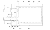
- 3A is a top view of the electrochemical device showing the first embodiment of the present invention
- FIG. 3B is a cross-sectional view taken along line S11-S11 in FIG. 3A
- FIG. 3 (A) is an enlarged sectional view taken along line S12-S12
- FIG. 3 (D) is an enlarged sectional view taken along line S13-S13 in FIG. 3 (A).
- 4 (A) and 4 (B) are for terminal derivation when the electrochemical device shown in FIGS. 3 (A) to 3 (D) is reflow soldered to a circuit board or encapsulated in an IC card. It is a figure for demonstrating the behavior of the heat seal material of a sealing part.
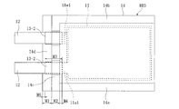
- FIG. 5 is a top view of an electrochemical device showing a second embodiment of the present invention.
- FIG. 6 is a top view of an electrochemical device showing a third embodiment of the present invention.
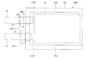
- FIG. 7 is a top view of an electrochemical device showing a fourth embodiment of the present invention.
- FIGS. 3A to 3D show an electrochemical device RB1 according to a first embodiment of the present invention.
- the electrochemical device RB1 includes a power storage element 11, a pair of terminals 12 electrically connected to the power storage element 11, a heat seal auxiliary member 13 provided at each terminal 12, and a film enclosing the power storage element 11 And a package 14.
- the power storage element 11 has a substantially rectangular outline in top view, and a collector electrode layer 11a, a polarizable electrode layer 11b, a separate film 11c, a polarizable electrode layer 11d, and a collector electrode layer 11e are stacked in this order from top to bottom.
- the collector electrode layers 11a and 11e are made of a conductive material such as aluminum or platinum and have a thickness of 5 to 50 ⁇ m.
- the polarizable electrode layers 11b and 11d are made of an active material such as PAS (polyacenic organic semiconductor) or activated carbon, and have a thickness of 10 to 100 ⁇ m.
- the seperate film 11c is made of an ion permeable film such as a cellulose film or a plastic film, and has a thickness of 10 to 50 ⁇ m.
- FIG. 3B shows the power storage element 11 having a five-layer structure for convenience of illustration. If the collector electrode layer, the polarizable electrode layer, and the separate film are laminated in a predetermined order, the number of layers is as follows. It can be increased as appropriate.
- Each terminal 12 has a substantially rectangular outline in top view, the rear end of one terminal 12 is electrically connected to one terminal connection portion 11 a 1 of the power storage element 11, and the rear end of the other terminal 12 is power storage element 11.
- the other terminal connection portion 11e1 is electrically connected.
- Each terminal 12 is made of a conductive material such as aluminum or platinum and has a thickness of 50 to 150 ⁇ m.
- a metal film such as tin or gold is formed on the front end of each terminal 12 by plating for soldering.
- Each heat seal auxiliary member 13 is provided so as to surround a part of each terminal 12.
- Each heat seal auxiliary member 13 is made of the same material as the heat seal layer LF3 described later, and has a thickness of 30 to 50 ⁇ m.
- Each heat seal auxiliary member 13 can be provided on each terminal 12 by applying a liquid material to the surface of the terminal 12 and curing it, or by winding a sheet-like material around the surface of the terminal 12.
- the film package 14 has a substantially rectangular top view outline, and is formed using a laminate film LF having a heat-resistant layer LF1, a barrier layer LF2, and a heat seal layer LF3 in this order.
- the heat-resistant layer LF1 is made of a thermoplastic such as nylon or polyethylene phthalate and has a thickness of 10 to 50 ⁇ m.
- the barrier layer LF2 is made of a metal such as aluminum or a metal oxide and has a thickness of 10 to 50 ⁇ m.
- the heat seal layer LF3 is made of a thermoplastic plastic such as polypropylene or modified polypropylene, and has a thickness of 30 to 50 ⁇ m.
- the left sealing portion 14a, the right sealing portion 14b, and the front sealing portion 14c (hereinafter referred to as terminals) formed by heat-sealing and integrating the heat seal layers LF3 together.
- the lead-out sealing portion 14c) is continuously formed with a predetermined width.
- the film package 14 has the lower film end on the terminal lead-out sealing portion 14c side protruding forward from the upper film end, and the support portion 14d formed by the projecting portion is connected to the terminal lead-out sealing. It has continuously along the part 14c.
- a portion of the lower film of the film package 14 that protrudes forward from the upper film that faces it may be referred to as a support portion 14d.
- the lower film end on the terminal lead-out sealing portion 14c side has the support portion 14d protruding forward from the upper film end on the terminal lead-out sealing portion 14c side, and the terminal lead-out sealing portion 14c. It has continuously along.
- the electricity storage element 11 is enclosed together with an electrolyte (for example, a liquid material obtained by adding triethylmethylammonium borofluoride to propylene carbonate as a solvent, or a gel material obtained by adding polyacrylonitrile or the like).
- an electrolyte for example, a liquid material obtained by adding triethylmethylammonium borofluoride to propylene carbonate as a solvent, or a gel material obtained by adding polyacrylonitrile or the like.
- each heat seal auxiliary projecting forward from the terminal derivation sealing portion 14c.
- the protrusion length of the front portion of the member 13 is substantially the same as the protrusion length M1 of the support portion 14d.
- the front-rear length M3 of each heat seal auxiliary member 13 is slightly larger than M1 + M2, and the rear end of each heat seal auxiliary member 13 protrudes into the film package 14 by a dimension M4.
- the storage element 11 to which each terminal 12 with the heat seal auxiliary member 13 is connected is prepared, and a rectangular laminate film LF having a predetermined size is prepared. Subsequently, the laminate film LF is arranged so that the heat seal layer LF3 faces upward, and the storage element 11 is mounted on the laminate film LF so that the front end of each heat seal auxiliary member 13 is substantially coincident with one film end. Put.
- the laminate film LF is folded in half so that the lower film end protrudes forward by the dimension M1 from the upper film end, and the left and right edges are heated to a predetermined width using an appropriate heating device.
- the left sealing part 14a and the right sealing part 14b are formed by heat-sealing and integrating the heat seal layers LF3 by the heating.
- an electrolyte is injected into the inside of the laminated film LF in the form of a bag from the front open portion, and the front edge of the laminated film LF is heated to a predetermined width using an appropriate heating device, and heat sealing is performed by the heating.
- the terminal LF3 sealing portion 14c is formed by heat-sealing and integrating the layers LF3.
- each heat seal auxiliary member 13 is made of the same material as the heat seal layer LF3, the heat seal layer LF3 and the rear side portion of each heat seal auxiliary member 13 are integrated by heating, and a part of each terminal 12 is this It is surrounded by “integrated heat seal material” without a gap (see FIG. 3D).
- a heating device having a hard heating surface is used in forming the portion 14c, the sealing capability of the thin portion is lower than that of the thick portion, and “integrated heat sealing”
- the “material” protrudes from the front edge or the rear edge of the terminal lead-out sealing portion 14c, but if a heating device having a heating surface that can be elastically deformed is used, the terminal lead-out sealing portion 14c does not cause such a problem. Can be formed.
- surface steps as shown in FIG. 3D appear on the upper and lower surfaces of the terminal lead-out sealing portion 14c based on the thickness difference, and accordingly, on the upper and lower surfaces of the support portion 14d.
- a surface level difference appears. That is, since the front portion of each heat seal auxiliary member 13 is held by the surface step appearing on the upper surface of the support portion 14d, the front portion of each heat seal auxiliary member 13 is displaced from side to side, that is, each terminal. It is possible to prevent the front portion of 12 from being displaced from side to side.
- 3 (C) and 3 (D) show a form in which the surface step is continuous on the slope for convenience of illustration, but in the case of using a heating instrument having an elastically deformable heating surface. Is such that the surface step is continuous on a curved surface.
- both terminals 12 of the electrochemical device RB1 are bent as necessary, and then both terminals 12 are connected to the electrode pads of the circuit board via cream solder.
- the external electrodes of electronic components such as chip capacitors and chip registers are disposed on the electrode pads of the circuit board via cream solder. And the circuit board after arrangement
- the electrochemical device RB1 on the circuit board is subjected to a soldering process according to a temperature profile of reflow soldering, whereby each terminal 12 is electrically joined to the electrode pad via the solder.
- the peak temperature when the solder is composed of lead-free solder is approximately 240 to 260 ° C. This peak temperature varies somewhat depending on the solder component.
- an IC module (a module in which an IC and other electronic components are modularized) is housed in a module housing through hole of the core sheet.
- another sheet including the module may be interposed between the core sheet and the lower cover sheet.
- the core sheet and upper and lower cover sheets are heat-sealed according to the heat-seal temperature profile. By this treatment, the sheets are brought into close contact with each other, and the electrochemical device RB1 is sealed in the IC card.
- the peak temperature when the core sheet and the upper and lower cover sheets are made of polyethylene phthalate is approximately 260 ° C. This peak temperature varies somewhat depending on the sheet component.
- the electrochemical device RB1 rises to each peak temperature or a temperature close thereto.
- the front portion of each terminal 12, the front portion of each heat seal auxiliary member 13, and the support portion 14d of the film package 14 do not have means for suppressing these temperature rises. It rises to a temperature close to.
- the heat-resistant layer LF1 is present on the surface of the film package 14 and the barrier layer LF2 is present on the inner side thereof, the storage element 11 and the electrolyte in the film package 14 are delayed from the front portion of each terminal 12 and the like. As a result, a similar temperature rise occurs.
- each terminal 12 is made of aluminum and each heat seal auxiliary member 13 and the heat seal layer LF3 of the support portion 14d are made of polypropylene (melting point is 170 ° C.)
- the rising temperature is the melting point of each heat seal auxiliary member 13. Therefore, the front side portion of each heat seal auxiliary member 13 and the heat seal layer LF3 of the support portion 14d are melted by the temperature rise.
- each heat seal auxiliary member 13 melts so as to spread along the surface of each terminal 12 as indicated by reference numeral 13 'in FIG.
- the front portion of each heat seal auxiliary member 13 is located on the support portion 14 and a melt of the seal layer LF3 made of the same material is present on the surface of the support portion 14. Although its shape changes upon melting, the melt remains at or near its original position.
- each terminal 12 rises, heat is transmitted through each terminal 12 to an “integrated heat seal material” that surrounds a part of each terminal 12 in the terminal lead-out sealing portion 14 c without a gap. .
- heat is transferred into the film package 14 through the heat-resistant layer LF1 and the barrier layer LF2, and the internal pressure rises due to an increase in the vapor pressure of the electrolyte.
- the “integrated heat seal material” that surrounds a part of each terminal 12 without gap is softened or melted by the heat conduction, and the force to push it outward acts on the rising internal pressure of the film package 14. To do.
- each heat seal auxiliary member 13 stops on the front side of the terminal lead-out sealing portion 14c corresponding to each terminal 12, so that the heat conduction from each terminal 12 softens or Even if the force to push the melted “integrated heat seal material” to the outside acts based on the rising internal pressure of the film package 14, the softened or melted “integrated heat seal material” is pushed to the outside. Is prevented. That is, the gap VO as shown in FIG. 2 is not formed around the portion of each terminal 12 located in the terminal derivation sealing portion 14c.
- each heat seal auxiliary member 13 When the temperature profile of reflow soldering or the temperature profile of heat seal shifts to cooling, the melt in the front portion of each heat seal auxiliary member 13 is sealed as indicated by reference numeral 13 ′′ in FIG.
- the “integrated heat seal material” that is rounded and solidified so as to approach the stop portion 14c and that surrounds a part of each terminal 12 without a gap is also solidified while maintaining the initial form.
- the “integrated heat seal material” that surrounds a part of each terminal 12 located in the terminal lead-out sealing portion 14c without a gap due to the presence of each heat seal auxiliary member 13 is provided. Since the thickness can be increased, the softening or melting of the “integrated heat seal material” can be delayed with the thickness, whereby the softened or melted “integrated heat seal material” is pushed out to the outside. Can be prevented more effectively.
- FIG. 5 shows an electrochemical device RB2 according to a second embodiment of the present invention.
- the electrochemical device RB2 is structurally different from the electrochemical device RB1 in that each of the heat seal auxiliary members 13-1 having a longer front and rear length M3 than the heat seal auxiliary members 13 is used.
- the front end of the auxiliary member 13-1 is protruded forward from the front edge of the support portion 14d by a dimension M5. That is, the protrusion length (M1 + M5) of the front side portion of each heat seal auxiliary member 13-1 protruding forward from the terminal lead-out sealing portion 14c of the film package 14 is longer than the protrusion length M1 of the support portion 13d.
- FIG. 6 shows an electrochemical device RB3 according to a third embodiment of the present invention.
- This electrochemical device RB3 is structurally different from the electrochemical device RB1 in that the front and rear length M3 is shorter than each heat seal auxiliary member 13 and used as each heat seal auxiliary member 13-2.
- the front end of the auxiliary member 13-2 is retracted from the front edge of the support portion 14d by a dimension M6. That is, the protrusion length (M1-M6) of the front portion of each heat seal auxiliary member 13-2 protruding forward from the terminal lead-out sealing portion 14c of the film package 14 is shorter than the protrusion length M1 of the support portion 13d.
- FIG. 7 shows an electrochemical device RB4 according to a fourth embodiment of the present invention.
- the electrochemical device RB4 is structurally different from the electrochemical device RB1 in that two support portions 14d-1 corresponding to the front portion of each heat seal auxiliary member 13 are provided instead of the support portion 14 in the front portion.
- the width M8 is larger than the width M7, and the front side portion of each heat seal auxiliary member 13 is located at the center in the left-right direction on each support portion 14d-1.
- Each support portion 14d-1 can be easily formed by preparing a rectangular laminate film LF in which a portion matching one of the support portions 14d-1 is provided in advance at one film end when the film package 14 is formed. Can do.
- the protruding length of the front portion of each heat seal auxiliary member 13 protruding forward from the terminal lead-out sealing portion 14c is substantially the same as the protruding length of the support portion 14d-1.
- the heat seal auxiliary members having longer front and back lengths than the respective heat seal auxiliary members 13 are used as the respective heat seal auxiliary members.
- the front end of each support portion 14d-1 can be projected from the front edge.
- the heat seal auxiliary member having a length shorter than the heat seal auxiliary member 13 is used as each heat seal auxiliary member. The front end of the seal auxiliary member can be retracted from the front edge of each support portion 14d-1.
- the film package 14 is formed by folding the rectangular laminate film LF in two and the left side sealing portion 14a and the right side sealing portion. It is created by forming the terminal lead-out sealing portion 14c after forming the stop portion 14b.
- the film package 14 has two rectangular laminated films LF overlapped to form a left side sealing portion, a right side sealing portion, and a rear side sealing portion, and then lead out the terminal. It is created by forming a sealing portion for use. Even an electrochemical device using such a film package can obtain the same operations and effects as the electrochemical device RB1.
- the film package 14 is formed using a three-layer laminated film LF.
- the film package 14 may be a laminate film having a heat seal layer on one side, and may be formed using a laminate film other than a three-layer structure. Even an electrochemical device using such a film package can obtain the same operations and effects as the electrochemical device RB1.
- each heat seal auxiliary member 13 is formed so as to protrude into the film package 14 by the dimension M4.
- the dimension M4 is arbitrary.
- the rear end of each heat seal assisting member 13 may not protrude into the film package 14, that is, the dimension M4 may be zero or a value close to zero. Also in these electrochemical devices, the same operation and effect as the electrochemical device RB1 can be obtained.
- Various embodiments of the present invention can be widely applied to various electrochemical devices such as an electric double layer capacitor, a lithium ion capacitor, a redox capacitor, and a lithium ion battery.
- electrochemical devices such as an electric double layer capacitor, a lithium ion capacitor, a redox capacitor, and a lithium ion battery.
- RB1, RB2, RB3, RB4 ... electrochemical device, 11 ... electricity storage element, 12 ... terminal, 13, 13-1, 13-2 ... heat seal auxiliary member, 14 ... film package, 14a, 14b, 14c ... sealing part , 14d, 14d-1 ... support portion, LF ... laminate film, LF3 ... heat seal layer.
Landscapes
- Chemical & Material Sciences (AREA)
- Chemical Kinetics & Catalysis (AREA)
- Electrochemistry (AREA)
- General Chemical & Material Sciences (AREA)
- Engineering & Computer Science (AREA)
- Power Engineering (AREA)
- Microelectronics & Electronic Packaging (AREA)
- Electric Double-Layer Capacitors Or The Like (AREA)
- Sealing Battery Cases Or Jackets (AREA)
- Battery Mounting, Suspending (AREA)
Abstract
【課題】リフロー半田付け時にフィルムパッケージの内外を連通する空隙が端子導出用封止部内に形成されるこを防止できる電気化学デバイスを提供する。 【解決手段】電気化学デバイスRB1は、端子導出用封止部14cを有するフィルムパッケージ14と、蓄電素子11と、後端を蓄電素子11に電気的に接続され前側部分を端子導出用封止部14cを通じてフィルムパッケージ14外に導出された端子12とを備える。フィルムパッケージ14は端子導出用封止部14c側に支持部14dを有しており、端子12にはヒートシール補助部材13がその一部分を囲むように設けられ、該ヒートシール補助部材13の後側部分は端子導出用封止部14c内に位置していてヒートシール層LF3相互が熱融着されるときにこれらと一体化しており、且つ、該ヒートシール補助部材13の前側部分は端子導出用封止部14cから前方に突出していて支持部14d上に位置している。
Description
本発明は、蓄電素子をフィルムパッケージ内に封入した構造を備える電気化学デバイスに関する。
以下、図面を引用して背景技術を説明する。該説明では図1(A)の紙面手前側から見て左、右、下、上、手前、及び奥の方向をそれぞれ「前」、「後」、「左」、「右」、「上」、及び「下」と称すると共に、他の図のこれらに相当する方向をそれぞれ「前」、「後」、「左」、「右」、「上」、及び「下」と称する。
図1(A)及び図1(B)は従来において一般的な電気化学デバイスRBを示す。この電気化学デバイスRBは、蓄電素子101と、蓄電素子101に電気的に接続された1対の端子102と、蓄電素子101を封入したフィルムパッケージ103と、を備えている。
蓄電素子101は略矩形の上面視輪郭を有し、集電極層と分極性電極層とセパレートフィルムが所定順序で上下方向に積層された構造を有している。また、集電極層の前縁には左右一対の矩形状の端子接続部が、それぞれ該集電極層と一体に設けられている。この左側の端子接続部は一方極性として用いられ、右側の端子接続部は他方極性として用いられる。
各端子102は略矩形の上面視輪郭を有し、一方の端子102の後端は蓄電素子101の一方の端子接続部に電気的に接続され、他方の端子102の後端は蓄電素子101の他方の端子接続部に電気的に接続されている。各端子102は一般にアルミニウムや白金等の導電材から成る。
フィルムパッケージ103は略矩形の上面視輪郭を有し、耐熱層LF1とバリア層LF2とヒートシール層LF3を順に有するラミネートフィルムLFを用いて形成されている。ヒートシール層LF3は一般にポリプロピレン等の熱可塑性プラスチックから成る。また、フィルムパッケージ103の外縁には、ヒートシール層LF3相互を熱融着して一体化することによって形成された左側封止部103aと右側封止部103bと前側封止部103c(以下、「端子導出用封止部103c」と言う)が所定幅で連続して設けられている。
このフィルムパッケージ103内には蓄電素子101が電解質と共に封入されていて、各端子102の前側部分は端子導出用封止部103cを通じてフィルムパッケージ103外に導出されている。
前記フィルムパッケージ103を作成するときには、各端子102が接続された蓄電素子101を用意すると共に、所定サイズの矩形状ラミネートフィルムLFを用意する。続いて、ヒートシール層LF3が上を向くようにラミネートフィルムLFを配置し、各端子102の前側部分が一方のフィルム端から突出するように蓄電素子101を該ラミネートフィルムLF上に載置する。
続いて、下側のフィルム端に上側のフィルム端が揃うようにラミネートフィルムLFを2つ折りにし、適当な加熱器具を用いてその左縁と右縁を所定幅で加熱し、該加熱によりヒートシール層LF3相互を熱融着して一体化することによって左側封止部103aと右側封止部103bを形成する。続いて、袋状となったラミネートフィルムLFの前側開放部分から電解質をその内側に注入し、適当な加熱器具を用いて該ラミネートフィルムLFの前縁を所定幅で加熱し、該加熱によりヒートシール層LF3相互を熱融着して一体化することによって端子導出用封止部103cを形成する。
端子導出用封止部103cを形成する際の加熱は、上下2つのヒートシール層LF3の間に各端子103の一部分を挟み込んだ状態で行われるため、該加熱によって上下2つのヒートシール層LF3は一体化し、各端子102の一部分はこの「一体化したヒートシール材料」によって隙間無く囲まれる(図1(B)を参照)。
ところで、前記電気化学デバイスRBは、フィルムパッケージ103を用いることによって他の蓄電デバイスに比べて薄型化が容易であることから、(1)電気化学デバイスRBをチップコンデンサやチップレジスタ等の電子部品と一緒に回路基板にリフロー半田付けする要望や(2)電気化学デバイスRBをICカード内に封入する要望が高まっている。
しかしながら、電気化学デバイスRBを回路基板にリフロー半田付けするときには、回路基板上に電気化学デバイスRBを搭載して該回路基板をリフロー炉に投入する手順が一般に採用されるため、リフロー半田付けの温度プロファイルに伴った温度上昇が電気化学デバイスRBに生じて、該電気化学デバイスRBがリフロー半田付けのピーク温度或いはこれに近い温度まで上昇してしまう。
一方、電気化学デバイスRBをICカード内に封入するときには、コアシートのデバイス収納用貫通孔に電気化学デバイスRBを収納して該コアシートの上下面それぞれにカバーシートをヒートシールする手順が一般に採用されるため、ヒートシールの温度プロファイルに伴った温度上昇が電気化学デバイスRBに生じて、該電気化学デバイスRBがヒートシールのピーク温度或いはこれに近い温度まで上昇してしまう。
この上昇温度が「一体化したヒートシール材料」の融点よりも高い場合には、前記温度上昇によって各端子102の一部分を隙間無く囲む「一体化したヒートシール材料」に軟化或いは溶融が生じると共に、フィルムパッケージ103の内圧が電解質の蒸気圧上昇等によって上昇する。
つまり、軟化或いは溶融した「一体化したヒートシール材料」がフィルムパッケージ103の上昇内圧によって外部に押し出される現象を生じる恐れがある。このように「一体化したヒートシール材料」が押し出された場合には、フィルムパッケージ103の内外を連通する空隙VOが各端子102の端子導出用封止部101c内に位置する部分の周囲に形成されてしまう(図2を参照)。
この現象によって、様々な位置に様々な大きさの空隙VOが形成され得る。該空隙VOがフィルムパッケージ103の内外を連通するように形成されてしまうと、該空隙VOを通じてフィルムパッケージ103内の電解質が外部に漏出して周囲を汚してしまったり、また、該電解質の漏出によって電気化学デバイスRBの機能が低下してしまったりする等の不具合を生じる。
本発明の目的は、電気化学デバイスを回路基板にリフロー半田付けする場合やICカード内に封入する場合でも、フィルムパッケージの内外を連通する空隙が端子導出用封止部内に形成されることを防止できる電気化学デバイスを提供することにある。
前記目的を達成するため、本発明の一実施形態は、ヒートシール層を有するラミネートフィルムを用いて作成されヒートシール層相互を熱融着して一体化することによって形成された端子導出用封止部を有するフィルムパッケージと、フィルムパッケージ内に封入された蓄電素子と、一端を蓄電素子に電気的に接続され他側部分を端子導出用封止部を通じてフィルムパッケージ外に導出された端子とを備える電気化学デバイスであって、フィルムパッケージは端子導出用封止部側の一方のフィルム端が他方のフィルム端よりも外方に突出するようになっていて該突出部分によって形成された支持部を有しており、端子にはヒートシール層と同一材料から成るヒートシール補助部材がその一部分を囲むように設けられ、該ヒートシール補助部材の一側部分は端子導出用封止部内に位置していてヒートシール層相互が熱融着されるときにこれらと一体化しており、且つ、該ヒートシール補助部材の他側部分は端子導出用封止部から外方に突出していて支持部上に位置している。
この電気化学デバイスを回路基板にリフロー半田付けする場合には、リフロー半田付けの温度プロファイルに伴った温度上昇が該電気化学デバイスに生じて、該電気化学デバイスがリフロー半田付けのピーク温度或いはこれに近い温度まで上昇してしまう。また、電気化学デバイスをICカード内に封入するときには、ヒートシールの温度プロファイルに伴った温度上昇が該電気化学デバイスに生じて、該電気化学デバイスがヒートシールのピーク温度或いはこれに近い温度まで上昇してしまう。
この上昇温度がヒートシール補助部材の融点よりも高い場合には前記温度上昇によってヒートシール補助部材の他側部分は端子の表面に沿って広がるように溶融するが、該各ヒートシール補助部材は支持部上に位置していることから、各ヒートシール補助部材の他側部分は溶融によってその形を変化するものの、該溶融物は当初位置或いはこれに近い位置に止まる。
一方、端子の温度上昇に伴って、該端子を介して、端子導出用封止部内において端子の一部分を囲む「一体化したヒートシール材料」に熱が伝わる。また、フィルムパッケージの表面の温度上昇に伴って該フィルムパッケージ内に熱が伝わり、電解質の蒸気圧上昇等によってその内圧が上昇する。つまり、端子の一部分を囲む「一体化したヒートシール材料」は前記熱伝導により軟化或いは溶融し、これを外部に押し出そうとする力がフィルムパッケージの上昇内圧に基づいて作用する。
しかしながら、先に述べたように端子に対応する端子導出用封止部の前側にはヒートシール補助部材の溶融物が止まっているため、端子からの熱伝導により軟化或いは溶融した「一体化したヒートシール材料」を外部に押し出そうとする力がフィルムパッケージの上昇内圧に基づいて作用しても、軟化或いは溶融した「一体化したヒートシール材料」が外部に押し出されることが阻止される。つまり、端子の端子導出用封止部内に位置する部分の周囲には、従前のような空隙が形成されることは無い。
よって、前記電気化学デバイスを回路基板にリフロー半田付けする場合やICカード内に封入する場合でも、フィルムパッケージの内外を連通する空隙が端子導出用封止部内に形成されることが無いため、該空隙を通じてフィルムパッケージ内の電解質が外部に漏出して周囲を汚してしまったり、また、該電解質の漏出によって電気化学デバイスの機能が低下する等の不具合を確実に回避できる。
本発明の一実施形態によれば、電気化学デバイスを回路基板にリフロー半田付けする場合やICカード内に封入する場合でも、フィルムパッケージの内外を連通する空隙が端子導出用封止部内に形成されることが無いため、該空隙を通じてフィルムパッケージ内の電解質が外部に漏出して周囲を汚してしまったり、また、該電解質の漏出によって電気化学デバイスの機能が低下する等の不具合を確実に回避できる。
本発明の前記目的とそれ以外の目的と、構成特徴と、作用効果は、以下の説明と添付図面によってさらに明らかとなる。
以下、図面を引用して発明を実施するための形態を説明するが、該説明では図3(A)の左、右、下、上、手前、及び奥をそれぞれ「前」、「後」、「左」、「右」、「上」、及び「下」と称すると共に、他の図のこれらに相当する方向をそれぞれ「前」、「後」、「左」、「右」、「上」、及び「下」と称する。
第1実施形態
図3(A)~図3(D)は本発明の第1実施形態に係る電気化学デバイスRB1を示す。この電気化学デバイスRB1は、蓄電素子11と、蓄電素子11に電気的に接続された1対の端子12と、各端子12に設けられたヒートシール補助部材13と、蓄電素子11を封入したフィルムパッケージ14と、を備えている。
図3(A)~図3(D)は本発明の第1実施形態に係る電気化学デバイスRB1を示す。この電気化学デバイスRB1は、蓄電素子11と、蓄電素子11に電気的に接続された1対の端子12と、各端子12に設けられたヒートシール補助部材13と、蓄電素子11を封入したフィルムパッケージ14と、を備えている。
蓄電素子11は略矩形の上面視輪郭を有し、集電極層11aと分極性電極層11bとセパレートフィルム11cと分極性電極層11dと集電極層11eがこの順序で上から下に向かって積層された構造を有している。集電極層11a及び11eはアルミニウムや白金等の導電材から成り、その厚さは5~50μmである。また、分極性電極層11b及び11dはPAS(ポリアセン系有機半導体)や活性炭等の活物質から成り、その厚さは10~100μmである。さらに、セパートフィルム11cはセルロース系フィルムやプラスチック系フィルム等のイオン透過フィルムから成り、その厚さは10~50μmである。
また、一方極性として用いられる集電極層11aの前縁の左側には矩形状の端子接続部11a1が該集電極層11aと一体に設けられ、他方極性として用いられる集電極層11eの前縁の右側には矩形状の端子接続部11e1が該集電極層11eと一体に設けられている。図3(B)には、図示の便宜上、5層構造の蓄電素子11を示したが、集電極層と分極性電極層とセパレートフィルムが所定の順序で積層されていれば、その層数は適宜増加可能である。
各端子12は略矩形の上面視輪郭を有し、一方の端子12の後端は蓄電素子11の一方の端子接続部11a1に電気的に接続され、他方の端子12の後端は蓄電素子11の他方の端子接続部11e1に電気的に接続されている。各端子12はアルミニウムや白金等の導電材から成り、その厚さは50~150μmである。また、各端子12の前端には、半田付けのために錫や金等の金属膜がメッキにより形成されている。
各ヒートシール補助部材13は各端子12の一部分を囲むように設けられている。各ヒートシール補助部材13は後記ヒートシール層LF3と同一材料から成り、その厚さは30~50μmである。各ヒートシール補助部材13は、液状物を端子12の表面に塗布して硬化させることにより、又は、シート状物を端子12の表面に巻き付けることにより、各端子12に設けることができる。
フィルムパッケージ14は略矩形の上面視輪郭を有し、耐熱層LF1とバリア層LF2とヒートシール層LF3を順に有するラミネートフィルムLFを用いて形成されている。耐熱層LF1はナイロンやポリエチレンフタレート等の熱可塑性プラスチックから成り、その厚さは10~50μmである。また、バリア層LF2はアルミニウム等の金属或いは金属酸化物から成り、その厚さは10~50μmである。さらに、ヒートシール層LF3はポリプロピレンや変性ポリプロピレン等の熱可塑性プラスチックから成り、その厚さは30~50μmである。
また、フィルムパッケージ14の外縁には、ヒートシール層LF3相互を熱融着して一体化することによって形成された左側封止部14aと右側封止部14bと前側封止部14c(以下、端子導出用封止部14cと言う)が所定幅で連続して形成される。さらに、フィルムパッケージ14は、端子導出用封止部14c側の下側のフィルム端が上側のフィルム端よりも前方に突出していて、該突出部分によって形成された支持部14dを端子導出用封止部14cに沿って連続して有している。つまり、本明細書においては、フィルムパッケージ14の下側のフィルムのうち、対向する上側のフィルムよりも前方に突出した部分を支持部14dと称することがある。換言すれば,端子導出用封止部14c側の下側のフィルム端は,端子導出用封止部14c側の上側のフィルム端よりも前方に突出する支持部14dを端子導出用封止部14cに沿って連続して有する。
このフィルムパッケージ14内には蓄電素子11が電解質(例えば硼弗化トリエチルメチルアンモニウムを溶媒であるプロピレンカーボネイトに加えた液状のものやこれにポリアクリロニトリル等を加えてゲル状にしたもの等)と共に封入されていて、各端子12の前側部分と各ヒートシール補助部材13の前側部分は端子導出用封止部14cを通じてフィルムパッケージ14外に導出されている。また、各ヒートシール補助部材13の後側部分は端子導出用封止部14c内に位置していてヒートシール層LF3相互が熱融着されるときにこれらと一体化しており、且つ、該各ヒートシール補助部材13の前側部分は端子導出用封止部14cから前方に突出していて支持部14d上に位置している。
図3(A)から分かるように、支持部14dの突出長をM1とし端子導出用封止部14cの幅をM2としたとき、端子導出用封止部14cから前方に突出する各ヒートシール補助部材13の前側部分の突出長は支持部14dの突出長M1と略一致している。また、各ヒートシール補助部材13の前後長M3はM1+M2よりも僅かに大きく、該各ヒートシール補助部材13の後端は寸法M4だけフィルムパッケージ14内に突出している。
前記フィルムパッケージ14を作成するときには、ヒートシール補助部材13付きの各端子12が接続された蓄電素子11を用意すると共に、所定サイズの矩形状ラミネートフィルムLFを用意する。続いて、ヒートシール層LF3が上を向くようにラミネートフィルムLFを配置し、各ヒートシール補助部材13の前端が一方のフィルム端と略一致するように蓄電素子11を該ラミネートフィルムLF上に載置する。
続いて、下側のフィルム端が上側のフィルム端よりも前方に寸法M1だけ突出するようにラミネートフィルムLFを2つ折りにし、適当な加熱器具を用いてその左縁と右縁を所定幅で加熱し、該加熱によりヒートシール層LF3相互を熱融着して一体化することによって左側封止部14aと右側封止部14bを形成する。続いて、袋状となったラミネートフィルムLFの前側開放部分から電解質をその内側に注入し、適当な加熱器具を用いて該ラミネートフィルムLFの前縁を所定幅で加熱し、該加熱によりヒートシール層LF3相互を熱融着して一体化することによって端子導出用封止部14cを形成する。
端子導出用封止部14cを形成する際の加熱は、上下2つのヒートシール層LF3の間に各ヒートシール補助部材13の後側部分を挟み込んだ状態で行われる。各ヒートシール補助部材13は、ヒートシール層LF3と同一材料から成るため、該加熱によってヒートシール層LF3と各ヒートシール補助部材13の後側部分とが一体化され、各端子12の一部分はこの「一体化したヒートシール材料」によって隙間無く囲まれる(図3(D)を参照)。
端子導出用封止部14cにおいて端子12の一部分とヒートシール補助部材13の後側部分が存する部分の厚さは他の部分の厚さに比べて僅かに厚くなるため、該端子導出用封止部14cを形成する際に硬質の加熱面を有する加熱器具を用いると、厚さの薄い部分のシール能力が厚さの厚い部分のシール能力よりも低下したり、また、「一体化したヒートシール材料」が端子導出用封止部14cの前縁または後縁からはみ出してしまうが、弾性変形可能な加熱面を有する加熱器具を用いればこのような不具合を生じることなく端子導出用封止部14cを形成できる。
また、前記の厚さの差に基づいて端子導出用封止部14cの上面及び下面に図3(D)に示したような表面段差が現れ、これに伴って支持部14dの上面及び下面にも図3(C)に示したような表面段差が現れる。つまり、各ヒートシール補助部材13の前側部分は支持部14dの上面に現れる表面段差によって保持されるため、該各ヒートシール補助部材13の前側部分が左右に位置ずれを生じること、即ち、各端子12の前側部分が左右に位置ずれを生じることが防止される。図3(C)及び図3(D)には、図示の便宜上、表面段差が斜面にて連続している形態を示してあるが、弾性変形可能な加熱面を有する加熱器具を用いた場合には該表面段差は曲面にて連続したような形態となる。
前記電気化学デバイスRB1を回路基板にリフロー半田付けするときには、電気化学デバイスRB1の両端子12の前側部分を必要に応じて折り曲げてから、該両端子12をクリーム半田を介して回路基板の電極パッド上に配置すると共に、チップコンデンサやチップレジスタ等の電子部品の外部電極をクリーム半田を介して回路基板の電極パッド上に配置する。そして、配置後の回路基板をリフロー炉に投入する。
回路基板上の電気化学デバイスRB1にはリフロー半田付けの温度プロファイルに準じて半田付け処理が施され、これにより各端子12は半田を介して電極パッドに電気的に接合される。半田が鉛フリー半田から成る場合のピーク温度は概ね240~260℃である。このピーク温度は半田成分によって多少変化する。
一方、前記電気化学デバイスRB1をICカードに封入するときには、ポリ塩化ビニルやポリエチレンフタレート等の熱可塑性プラスチックから成るコアシート及び2枚のカバーシートを用意し、コアシートのデバイス収納用貫通孔に電気化学デバイスRB1を収納し、該コアシートの上下面にカバーシートを重ね合わせる。そして、適当な加熱器具を用いてコアシートと上下のカバーシートを加圧しながらシート相互をヒートシールする。一実施形態においては、ICモジュール(ICと他の電子部品等がモジュール化されたもの)はコアシートのモジュール収納用貫通孔に収納される。他の実施形態において、該モジュールを含む別シートをコアシートと下側のカバーシートとの間に介装するようにしても良い。
コアシートと上下のカバーシートにはヒートシールの温度プロファイルに準じてヒートシール処理が施される。この処理によりシート相互が密着して電気化学デバイスRB1がICカード内に封入される。コアシート及び上下のカバーシートがポリエチレンフタレートから成る場合のピーク温度は概ね260℃である。このピーク温度はシート成分によって多少変化する。
このように、前者の場合にはリフロー半田付けの温度プロファイルに伴った温度上昇が電気化学デバイスRB1に生じ、後者の場合にはヒートシールの温度プロファイルに伴った温度上昇が電気化学デバイスRB1に生じるため、何れの場合も電気化学デバイスRB1は各々のピーク温度或いはこれに近い温度まで上昇してしまう。
詳しくは、各端子12の前側部分や各ヒートシール補助部材13の前側部分やフィルムパッケージ14の支持部14dはこれらの温度上昇を抑制する手段が無いため、これらは短時間で前記ピーク温度或いはこれに近い温度まで上昇する。これに対し、フィルムパッケージ14の表面には耐熱層LF1が在りその内側にはバリア層LF2が在るため、フィルムパッケージ14内の蓄電素子11や電解質は各端子12の前側部分等よりも遅れるようにして同様の温度上昇を生じることになる。
つまり、各端子12がアルミニウムから成り、各ヒートシール補助部材13と支持部14dのヒートシール層LF3がポリプロピレン(融点は170℃)から成る場合には、上昇温度が各ヒートシール補助部材13の融点よりも高いために、前記温度上昇によって各ヒートシール補助部材13の前側部分と支持部14dのヒートシール層LF3は溶融する。
このとき、各ヒートシール補助部材13の前側部分は、図4(A)に符号13’で示したように各端子12の表面に沿って広がるように溶融するが、該各ヒートシール補助部材13の前側部分は支持部14上に位置していて、且つ、該支持部14の表面には同一材料から成るシール層LF3の溶融物が在ることから、各ヒートシール補助部材13の前側部分は溶融によってその形を変化するものの、該溶融物は当初位置或いはこれに近い位置に止まる。
一方、各端子12の温度上昇に伴って、該各端子12を介して、端子導出用封止部14c内において各端子12の一部分を隙間無く囲む「一体化したヒートシール材料」に熱が伝わる。また、フィルムパッケージ14の表面の温度上昇に伴って、耐熱層LF1とバリア層LF2を介して、該フィルムパッケージ14内に熱が伝わり、電解質の蒸気圧上昇等によってその内圧が上昇する。つまり、各端子12の一部分を隙間無く囲む「一体化したヒートシール材料」は前記熱伝導により軟化或いは溶融し、これを外部に押し出そうとする力がフィルムパッケージ14の上昇内圧に基づいて作用する。
しかしながら、先に述べたように各端子12に対応する端子導出用封止部14cの前側には各ヒートシール補助部材13の溶融物が止まっているため、各端子12からの熱伝導により軟化或いは溶融した「一体化したヒートシール材料」を外部に押し出そうとする力がフィルムパッケージ14の上昇内圧に基づいて作用しても、軟化或いは溶融した「一体化したヒートシール材料」が外部に押し出されることが阻止される。つまり、各端子12の端子導出用封止部14c内に位置する部分の周囲には、図2に示したような空隙VOが形成されることは無い。
リフロー半田付けの温度プロファイルやヒートシールの温度プロファイルが冷却に移行すると、各ヒートシール補助部材13の前側部分の溶融物は、図4(B)に符号13”で
示したように端子導出用封止部14cに近寄るように丸みを帯びて固化し、且つ、各端子12の一部分を隙間無く囲む「一体化したヒートシール材料」も当初形態を維持したままで固化する。
示したように端子導出用封止部14cに近寄るように丸みを帯びて固化し、且つ、各端子12の一部分を隙間無く囲む「一体化したヒートシール材料」も当初形態を維持したままで固化する。
このように、前記電気化学デバイスRB1を回路基板にリフロー半田付けする場合やICカード内に封入する場合でも、フィルムパッケージ14の内外を連通する空隙が端子導出用封止部14c内に形成されることが無いため、該空隙を通じてフィルムパッケージ14内の電解質が外部に漏出して周囲を汚してしまったり、また、該電解質の漏出によって電気化学デバイスRB1の機能が低下してしまったりする等の不具合を確実に回避できる。
また、前記電気化学デバイスRB1によれば、各ヒートシール補助部材13の存在によって、端子導出用封止部14c内に位置する各端子12の一部分を隙間無く囲む「一体化したヒートシール材料」の厚さを増加できるので、該厚さをもってして「一体化したヒートシール材料」の軟化或いは溶融を遅延させることができ、これにより軟化或いは溶融した「一体化したヒートシール材料」が外部に押し出されることをより効果的に阻止できる。
第2実施形態
図5は本発明の第2実施形態に係る電気化学デバイスRB2を示す。この電気化学デバイスRB2が、前記電気化学デバイスRB1と構造上で異なるところは、各ヒートシール補助部材13よりも前後長M3が長いものを各ヒートシール補助部材13-1として用い、該各ヒートシール補助部材13-1の前端を寸法M5だけ支持部14dの前縁から前方に突出させた点にある。つまり、フィルムパッケージ14の端子導出用封止部14cから前方に突出する各ヒートシール補助部材13-1の前側部分の突出長(M1+M5)は、支持部13dの突出長M1よりも長い。
図5は本発明の第2実施形態に係る電気化学デバイスRB2を示す。この電気化学デバイスRB2が、前記電気化学デバイスRB1と構造上で異なるところは、各ヒートシール補助部材13よりも前後長M3が長いものを各ヒートシール補助部材13-1として用い、該各ヒートシール補助部材13-1の前端を寸法M5だけ支持部14dの前縁から前方に突出させた点にある。つまり、フィルムパッケージ14の端子導出用封止部14cから前方に突出する各ヒートシール補助部材13-1の前側部分の突出長(M1+M5)は、支持部13dの突出長M1よりも長い。
この電気化学デバイスRB2であっても、前述の電気化学デバイスRB1と同様の作用,効果を得ることができる。
第3実施形態
図6は本発明の第3実施形態に係る電気化学デバイスRB3を示す。この電気化学デバイスRB3が、前記電気化学デバイスRB1と構造上で異なるところは、各ヒートシール補助部材13よりも前後長M3が短いものを各ヒートシール補助部材13-2として用い、該各ヒートシール補助部材13-2の前端を寸法M6だけ支持部14dの前縁から後退させた点にある。つまり、フィルムパッケージ14の端子導出用封止部14cから前方に突出する各ヒートシール補助部材13-2の前側部分の突出長(M1-M6)は、支持部13dの突出長M1よりも短い。
図6は本発明の第3実施形態に係る電気化学デバイスRB3を示す。この電気化学デバイスRB3が、前記電気化学デバイスRB1と構造上で異なるところは、各ヒートシール補助部材13よりも前後長M3が短いものを各ヒートシール補助部材13-2として用い、該各ヒートシール補助部材13-2の前端を寸法M6だけ支持部14dの前縁から後退させた点にある。つまり、フィルムパッケージ14の端子導出用封止部14cから前方に突出する各ヒートシール補助部材13-2の前側部分の突出長(M1-M6)は、支持部13dの突出長M1よりも短い。
この電気化学デバイスRB3であっても、前記電気化学デバイスRB1と同様の作用,効果を得ることができる。
第4実施形態
図7は本発明の第4実施形態に係る電気化学デバイスRB4を示す。この電気化学デバイスRB4が、前記電気化学デバイスRB1と構造上で異なるところは、支持部14の代わりに各ヒートシール補助部材13の前側部分に対応する2つの支持部14d-1を該前側部分の幅M7よりも大きな幅M8で形成し、各ヒートシール補助部材13の前側部分を各支持部14d-1上の左右方向中央に位置させた点にある。各支持部14d-1は、フィルムパッケージ14を作成するに際して、一方のフィルム端に予め各支持部14d-1に合致した部分を設けた矩形状ラミネートフィルムLFを用意することで簡単に形成することができる。
図7は本発明の第4実施形態に係る電気化学デバイスRB4を示す。この電気化学デバイスRB4が、前記電気化学デバイスRB1と構造上で異なるところは、支持部14の代わりに各ヒートシール補助部材13の前側部分に対応する2つの支持部14d-1を該前側部分の幅M7よりも大きな幅M8で形成し、各ヒートシール補助部材13の前側部分を各支持部14d-1上の左右方向中央に位置させた点にある。各支持部14d-1は、フィルムパッケージ14を作成するに際して、一方のフィルム端に予め各支持部14d-1に合致した部分を設けた矩形状ラミネートフィルムLFを用意することで簡単に形成することができる。
この電気化学デバイスRB4であっても、前記電気化学デバイスRB1と同様の作用,効果を得ることができる。
一実施形態においては,図7に示されるように,端子導出用封止部14cから前方に突出する各ヒートシール補助部材13の前側部分の突出長が支持部14d-1の突出長と略一致するように形成される。他の実施形態においては,前記第2実施形態に係る電気化学デバイスRB2と同様に、各ヒートシール補助部材13よりも前後長が長いものを各ヒートシール補助部材として用い、該各ヒートシール補助部材の前端を各支持部14d-1の前縁から突出させるようにすることができる。また、さらに他の実施形態においては,前記第3実施形態に係る電気化学デバイスRB3と同様に、各ヒートシール補助部材13よりも前後長が短いものを各ヒートシール補助部材として用い、該各ヒートシール補助部材の前端を各支持部14d-1の前縁から引っ込ませるようにすることができる。
他の実施形態
(1)前述の第1~第4実施形態(電気化学デバイスRB1~RB4)においては,フィルムパッケージ14は,矩形状ラミネートフィルムLFを2つ折りにして左側封止部14aと右側封止部14bを形成してから端子導出用封止部14cを形成することによって作成される。これに対し,他の実施形態においては,フィルムパッケージ14は,2枚の矩形状ラミネートフィルムLFを重ね合わせて左側封止部と右側封止部と後側封止部を形成してから端子導出用封止部を形成することによって作成される。このようなフィルムパッケージを用いた電気化学デバイスであっても、前記電気化学デバイスRB1と同様の作用,効果を得ることができる。
(1)前述の第1~第4実施形態(電気化学デバイスRB1~RB4)においては,フィルムパッケージ14は,矩形状ラミネートフィルムLFを2つ折りにして左側封止部14aと右側封止部14bを形成してから端子導出用封止部14cを形成することによって作成される。これに対し,他の実施形態においては,フィルムパッケージ14は,2枚の矩形状ラミネートフィルムLFを重ね合わせて左側封止部と右側封止部と後側封止部を形成してから端子導出用封止部を形成することによって作成される。このようなフィルムパッケージを用いた電気化学デバイスであっても、前記電気化学デバイスRB1と同様の作用,効果を得ることができる。
(2)前述の第1~第4実施形態(電気化学デバイスRB1~RB4)においては、フィルムパッケージ14は,3層構成ラミネートフィルムLFを用いて形成される。これに対し,他の実施形態においては,フィルムパッケージ14は,ヒートシール層を片面側に有するラミネートフィルムであればよく,3層構成以外のラミネートフィルムを用いて形成されてもよい。このようなフィルムパッケージを用いた電気化学デバイスであっても、前記電気化学デバイスRB1と同様の作用,効果を得ることができる。
(3)前述の第1~第4実施形態(電気化学デバイスRB1~RB4)では、各ヒートシール補助部材13の後端は,寸法M4だけフィルムパッケージ14内に突出するよう形成されているが、該寸法M4は任意である。他の実施形態においては、各ヒートシール補助部材13の後端がフィルムパッケージ14内に突出していなくても、即ち、寸法M4が零または零に近い数値であってもよい。これらの電気化学デバイスにおいても,前記電気化学デバイスRB1と同様の作用,効果を得ることができる。
本発明の様々な実施形態は、電気二重層キャパシタやリチウムイオンキャパシタやレドックスキャパシタやリチウムイオン電池等の各種電気化学デバイスに広く適用できる。本発明の様々な実施形態をこれらの電気化学デバイスに適用することによって,上述したのと同様の作用,効果を得ることができる。
RB1,RB2,RB3,RB4…電気化学デバイス、11…蓄電素子、12…端子、13,13-1,13-2…ヒートシール補助部材、14…フィルムパッケージ、14a,14b,14c…封止部、14d,14d-1…支持部、LF…ラミネートフィルム、LF3…ヒートシール層。
Claims (6)
- ヒートシール層を有するラミネートフィルムを用いて作成され前記ヒートシール層相互を熱融着して一体化することによって形成された端子導出用封止部を有するフィルムパッケージと、前記フィルムパッケージ内に封入された蓄電素子と、一端を前記蓄電素子に電気的に接続され他側部分を前記端子導出用封止部を通じてフィルムパッケージ外に導出された端子とを備える電気化学デバイスであって、
前記フィルムパッケージは前記端子導出用封止部側の一方のフィルム端が他方のフィルム端よりも外方に突出していて該突出部分によって形成された支持部を有しており、
端子には前記ヒートシール層と同一材料から成るヒートシール補助部材がその一部分を囲むように設けられ、該ヒートシール補助部材の一側部分は前記端子導出用封止部内に位置していてヒートシール層相互が熱融着されるときにこれらと一体化しており、且つ、該ヒートシール補助部材の他側部分は前記端子導出用封止部から外方に突出していてフィルムパッケージの支持部上に位置している。 - 請求項1に記載の電気化学デバイスにおいて、
フィルムパッケージの支持部は、前記端子導出用封止部に沿って連続して形成されている。 - 請求項1に記載の電気化学デバイスにおいて、
前記フィルムパッケージの前記支持部は、前記端子導出用封止部から外方に突出する前記ヒートシール補助部材の他側部分に対応して部分的に形成されており、該支持部の幅は、前記ヒートシール補助部材の他側部分の幅よりも大きい。 - 請求項1~3の何れか1項に記載の電気化学デバイスにおいて、
前記フィルムパッケージの前記端子導出用封止部から外方に突出する前記ヒートシール補助部材の他側部分の突出長は、前記支持部の突出長と略一致している。 - 請求項1~3の何れか1項に記載の電気化学デバイスにおいて、
前記フィルムパッケージの前記端子導出用封止部から外方に突出する前記ヒートシール補助部材の他側部分の突出長は、前記支持部の突出長よりも長い。 - 請求項1~3の何れか1項に記載の電気化学デバイスにおいて、
前記フィルムパッケージの前記端子導出用封止部から外方に突出する前記ヒートシール補助部材の他側部分の突出長は、支持部の突出長よりも短い。
Priority Applications (1)
| Application Number | Priority Date | Filing Date | Title |
|---|---|---|---|
| US13/574,533 US20130108917A1 (en) | 2010-01-21 | 2011-01-11 | Electrochemical device |
Applications Claiming Priority (2)
| Application Number | Priority Date | Filing Date | Title |
|---|---|---|---|
| JP2010-010676 | 2010-01-21 | ||
| JP2010010676A JP5349345B2 (ja) | 2010-01-21 | 2010-01-21 | 電気化学デバイス |
Publications (1)
| Publication Number | Publication Date |
|---|---|
| WO2011089944A1 true WO2011089944A1 (ja) | 2011-07-28 |
Family
ID=44306747
Family Applications (1)
| Application Number | Title | Priority Date | Filing Date |
|---|---|---|---|
| PCT/JP2011/050243 Ceased WO2011089944A1 (ja) | 2010-01-21 | 2011-01-11 | 電気化学デバイス |
Country Status (3)
| Country | Link |
|---|---|
| US (1) | US20130108917A1 (ja) |
| JP (1) | JP5349345B2 (ja) |
| WO (1) | WO2011089944A1 (ja) |
Families Citing this family (6)
| Publication number | Priority date | Publication date | Assignee | Title |
|---|---|---|---|---|
| JP2013197267A (ja) * | 2012-03-19 | 2013-09-30 | Kojima Press Industry Co Ltd | コンデンサ |
| MY195773A (en) | 2016-05-20 | 2023-02-11 | Kyocera Avx Components Corp | Multi-Cell Ultracapacitor |
| US11830672B2 (en) | 2016-11-23 | 2023-11-28 | KYOCERA AVX Components Corporation | Ultracapacitor for use in a solder reflow process |
| KR20240090881A (ko) * | 2018-03-30 | 2024-06-21 | 교세라 에이브이엑스 컴포넌츠 코포레이션 | 장벽층을 구비하는 슈퍼 커패시터 어셈블리 |
| JP2023539355A (ja) * | 2020-09-23 | 2023-09-13 | 寧徳新能源科技有限公司 | 電池 |
| WO2022133419A1 (en) * | 2020-12-15 | 2022-06-23 | Emerson Professional Tools, Llc | Power tool with hybrid supercapacitors |
Citations (6)
| Publication number | Priority date | Publication date | Assignee | Title |
|---|---|---|---|---|
| JP2002343681A (ja) * | 2001-05-11 | 2002-11-29 | Meidensha Corp | 電気二重層キャパシタ |
| JP2004319098A (ja) * | 2003-04-11 | 2004-11-11 | Sii Micro Parts Ltd | 電気化学セル及びその製造方法 |
| JP2004335889A (ja) * | 2003-05-09 | 2004-11-25 | Tdk Corp | 電気化学キャパシタ |
| JP2008135443A (ja) * | 2006-11-27 | 2008-06-12 | Nissan Diesel Motor Co Ltd | 電気二重層キャパシタ |
| JP2009043719A (ja) * | 2007-07-19 | 2009-02-26 | Sumitomo Electric Ind Ltd | リード部材及びその製造方法並びに非水電解質蓄電デバイス |
| JP2009253093A (ja) * | 2008-04-08 | 2009-10-29 | Taiyo Yuden Co Ltd | 電気化学デバイス |
Family Cites Families (9)
| Publication number | Priority date | Publication date | Assignee | Title |
|---|---|---|---|---|
| KR100342045B1 (ko) * | 1999-04-16 | 2002-06-27 | 김순택 | 2차전지 |
| EP1096589A1 (en) * | 1999-05-14 | 2001-05-02 | Mitsubishi Denki Kabushiki Kaisha | Flat battery and electronic device |
| JP2001102014A (ja) * | 1999-09-30 | 2001-04-13 | Mitsubishi Electric Corp | 板状電池および携帯無線端末 |
| CN1288769C (zh) * | 2001-01-18 | 2006-12-06 | 大日本印刷株式会社 | 电池以及引线绝缘膜 |
| JP2002319437A (ja) * | 2002-03-15 | 2002-10-31 | Japan Storage Battery Co Ltd | 電 池 |
| JP3758629B2 (ja) * | 2002-09-26 | 2006-03-22 | 日産自動車株式会社 | ラミネートシートおよびこれを用いたラミネート電池 |
| JP2005243453A (ja) * | 2004-02-26 | 2005-09-08 | Sii Micro Parts Ltd | 電気化学セル及びその製造方法 |
| JP5021961B2 (ja) * | 2006-06-16 | 2012-09-12 | Necエナジーデバイス株式会社 | ラミネート電池およびその製造方法 |
| JP5075464B2 (ja) * | 2007-04-19 | 2012-11-21 | シャープ株式会社 | 電源装置およびその製造方法 |
-
2010
- 2010-01-21 JP JP2010010676A patent/JP5349345B2/ja not_active Expired - Fee Related
-
2011
- 2011-01-11 WO PCT/JP2011/050243 patent/WO2011089944A1/ja not_active Ceased
- 2011-01-11 US US13/574,533 patent/US20130108917A1/en not_active Abandoned
Patent Citations (6)
| Publication number | Priority date | Publication date | Assignee | Title |
|---|---|---|---|---|
| JP2002343681A (ja) * | 2001-05-11 | 2002-11-29 | Meidensha Corp | 電気二重層キャパシタ |
| JP2004319098A (ja) * | 2003-04-11 | 2004-11-11 | Sii Micro Parts Ltd | 電気化学セル及びその製造方法 |
| JP2004335889A (ja) * | 2003-05-09 | 2004-11-25 | Tdk Corp | 電気化学キャパシタ |
| JP2008135443A (ja) * | 2006-11-27 | 2008-06-12 | Nissan Diesel Motor Co Ltd | 電気二重層キャパシタ |
| JP2009043719A (ja) * | 2007-07-19 | 2009-02-26 | Sumitomo Electric Ind Ltd | リード部材及びその製造方法並びに非水電解質蓄電デバイス |
| JP2009253093A (ja) * | 2008-04-08 | 2009-10-29 | Taiyo Yuden Co Ltd | 電気化学デバイス |
Also Published As
| Publication number | Publication date |
|---|---|
| US20130108917A1 (en) | 2013-05-02 |
| JP5349345B2 (ja) | 2013-11-20 |
| JP2011151171A (ja) | 2011-08-04 |
Similar Documents
| Publication | Publication Date | Title |
|---|---|---|
| JP5427239B2 (ja) | 電気化学キャパシタ | |
| JP5349345B2 (ja) | 電気化学デバイス | |
| US10193180B2 (en) | Method for manufacturing laminated electrical storage device | |
| TWI517192B (zh) | 一種儲能裝置的封裝結構 | |
| JP2016039091A (ja) | 電気化学セル、電気化学セルモジュール、携帯機器、および電気化学セルモジュールの製造方法 | |
| JP3931983B2 (ja) | 電気リード部の構造、該リード部構造を有する電気デバイス、電池および組電池 | |
| CN102918615B (zh) | 电化学器件 | |
| JP6491548B2 (ja) | 二次電池の製造方法および製造装置 | |
| CN109564990B (zh) | 电化学装置 | |
| US10418617B2 (en) | Laminate-type power storage element and manufacturing method thereof | |
| JP2009188195A (ja) | 電気化学デバイス及びその実装構造 | |
| JP2007273606A (ja) | ラミネートフィルム外装電子部品 | |
| JP2017134961A (ja) | ラミネート型蓄電素子およびラミネート型蓄電素子の実装方法 | |
| US10546700B2 (en) | Laminate-type power storage element and method of implementing the same | |
| JP2011222891A (ja) | 電気化学デバイス | |
| JP2009123889A (ja) | 電気化学デバイス及びその製造方法 | |
| CN107004824A (zh) | 电极 | |
| JP6986347B2 (ja) | ラミネート型蓄電素子およびラミネート型蓄電素子の実装方法 | |
| JP2007273625A (ja) | 電子部品及びその製造方法 | |
| JP2000286171A (ja) | 電気二重層コンデンサ | |
| JP3062551U (ja) | 非水系二次電池の封止構造 | |
| JP2004221575A (ja) | 積層型アルミニウム電解コンデンサ | |
| JP5626858B2 (ja) | ラミネートフィルム外装型二次電池 | |
| JP2018037338A (ja) | 蓄電素子 | |
| JPH02305426A (ja) | 電気二重層コンデンサとその製造方法 |
Legal Events
| Date | Code | Title | Description |
|---|---|---|---|
| 121 | Ep: the epo has been informed by wipo that ep was designated in this application |
Ref document number: 11734551 Country of ref document: EP Kind code of ref document: A1 |
|
| NENP | Non-entry into the national phase |
Ref country code: DE |
|
| WWE | Wipo information: entry into national phase |
Ref document number: 13574533 Country of ref document: US |
|
| 122 | Ep: pct application non-entry in european phase |
Ref document number: 11734551 Country of ref document: EP Kind code of ref document: A1 |