WO2011087028A1 - フィン一体型基板およびフィン一体型基板の製造方法 - Google Patents
フィン一体型基板およびフィン一体型基板の製造方法 Download PDFInfo
- Publication number
- WO2011087028A1 WO2011087028A1 PCT/JP2011/050381 JP2011050381W WO2011087028A1 WO 2011087028 A1 WO2011087028 A1 WO 2011087028A1 JP 2011050381 W JP2011050381 W JP 2011050381W WO 2011087028 A1 WO2011087028 A1 WO 2011087028A1
- Authority
- WO
- WIPO (PCT)
- Prior art keywords
- fin
- base plate
- metal base
- integrated substrate
- substrate according
- Prior art date
Links
- 239000000758 substrate Substances 0.000 title claims abstract description 113
- 238000004519 manufacturing process Methods 0.000 title claims abstract description 24
- 238000000034 method Methods 0.000 claims abstract description 53
- 239000000919 ceramic Substances 0.000 claims abstract description 43
- 229910052751 metal Inorganic materials 0.000 claims description 132
- 239000002184 metal Substances 0.000 claims description 132
- 230000005855 radiation Effects 0.000 claims description 38
- 238000005520 cutting process Methods 0.000 claims description 35
- 229910000838 Al alloy Chemical group 0.000 claims description 22
- 229910052782 aluminium Inorganic materials 0.000 claims description 22
- XAGFODPZIPBFFR-UHFFFAOYSA-N aluminium Chemical group [Al] XAGFODPZIPBFFR-UHFFFAOYSA-N 0.000 claims description 17
- 230000002093 peripheral effect Effects 0.000 claims description 7
- 239000013078 crystal Substances 0.000 claims description 5
- 238000005219 brazing Methods 0.000 claims description 4
- 229910052797 bismuth Inorganic materials 0.000 claims description 3
- 229910052749 magnesium Inorganic materials 0.000 claims description 3
- 229910052710 silicon Inorganic materials 0.000 claims description 3
- 229910052718 tin Inorganic materials 0.000 claims description 3
- 229910052725 zinc Inorganic materials 0.000 claims description 3
- 230000015572 biosynthetic process Effects 0.000 claims 1
- 238000004873 anchoring Methods 0.000 abstract 1
- 238000003780 insertion Methods 0.000 abstract 1
- 230000037431 insertion Effects 0.000 abstract 1
- 229910001338 liquidmetal Inorganic materials 0.000 abstract 1
- 238000007493 shaping process Methods 0.000 abstract 1
- 238000001816 cooling Methods 0.000 description 26
- 239000000463 material Substances 0.000 description 26
- 230000017525 heat dissipation Effects 0.000 description 13
- 238000012545 processing Methods 0.000 description 13
- 238000012360 testing method Methods 0.000 description 12
- 238000010438 heat treatment Methods 0.000 description 11
- 239000011295 pitch Substances 0.000 description 10
- 239000007788 liquid Substances 0.000 description 9
- 238000003825 pressing Methods 0.000 description 7
- 230000007797 corrosion Effects 0.000 description 6
- 238000005260 corrosion Methods 0.000 description 6
- 238000005304 joining Methods 0.000 description 5
- 238000003672 processing method Methods 0.000 description 5
- 230000001052 transient effect Effects 0.000 description 5
- 230000000052 comparative effect Effects 0.000 description 4
- 230000007423 decrease Effects 0.000 description 4
- 238000011156 evaluation Methods 0.000 description 4
- 229910052799 carbon Inorganic materials 0.000 description 3
- 238000005266 casting Methods 0.000 description 3
- 239000000110 cooling liquid Substances 0.000 description 3
- 239000000498 cooling water Substances 0.000 description 3
- 238000005259 measurement Methods 0.000 description 3
- 229920006395 saturated elastomer Polymers 0.000 description 3
- 239000004065 semiconductor Substances 0.000 description 3
- 230000035939 shock Effects 0.000 description 3
- 238000005476 soldering Methods 0.000 description 3
- OKTJSMMVPCPJKN-UHFFFAOYSA-N Carbon Chemical compound [C] OKTJSMMVPCPJKN-UHFFFAOYSA-N 0.000 description 2
- -1 aluminum Chemical class 0.000 description 2
- 239000002826 coolant Substances 0.000 description 2
- 239000004519 grease Substances 0.000 description 2
- 230000010354 integration Effects 0.000 description 2
- 150000002739 metals Chemical class 0.000 description 2
- 238000012986 modification Methods 0.000 description 2
- 230000004048 modification Effects 0.000 description 2
- 238000004088 simulation Methods 0.000 description 2
- 229910018072 Al 2 O 3 Inorganic materials 0.000 description 1
- 229910018566 Al—Si—Mg Inorganic materials 0.000 description 1
- BQCADISMDOOEFD-UHFFFAOYSA-N Silver Chemical compound [Ag] BQCADISMDOOEFD-UHFFFAOYSA-N 0.000 description 1
- 238000003848 UV Light-Curing Methods 0.000 description 1
- 229910045601 alloy Inorganic materials 0.000 description 1
- 239000000956 alloy Substances 0.000 description 1
- AZDRQVAHHNSJOQ-UHFFFAOYSA-N alumane Chemical group [AlH3] AZDRQVAHHNSJOQ-UHFFFAOYSA-N 0.000 description 1
- 239000012298 atmosphere Substances 0.000 description 1
- 150000001721 carbon Chemical class 0.000 description 1
- 239000002131 composite material Substances 0.000 description 1
- 230000008602 contraction Effects 0.000 description 1
- 238000007599 discharging Methods 0.000 description 1
- 238000005530 etching Methods 0.000 description 1
- 239000007789 gas Substances 0.000 description 1
- FBAFATDZDUQKNH-UHFFFAOYSA-M iron chloride Chemical compound [Cl-].[Fe] FBAFATDZDUQKNH-UHFFFAOYSA-M 0.000 description 1
- 239000007791 liquid phase Substances 0.000 description 1
- 238000003754 machining Methods 0.000 description 1
- 238000002844 melting Methods 0.000 description 1
- 230000008018 melting Effects 0.000 description 1
- 239000000203 mixture Substances 0.000 description 1
- 239000012299 nitrogen atmosphere Substances 0.000 description 1
- 238000007747 plating Methods 0.000 description 1
- 230000003014 reinforcing effect Effects 0.000 description 1
- 229910052709 silver Inorganic materials 0.000 description 1
- 239000004332 silver Substances 0.000 description 1
- 229910000679 solder Inorganic materials 0.000 description 1
- 238000007711 solidification Methods 0.000 description 1
- 230000008023 solidification Effects 0.000 description 1
- 238000012546 transfer Methods 0.000 description 1
- 238000003466 welding Methods 0.000 description 1
- NWONKYPBYAMBJT-UHFFFAOYSA-L zinc sulfate Chemical compound [Zn+2].[O-]S([O-])(=O)=O NWONKYPBYAMBJT-UHFFFAOYSA-L 0.000 description 1
Images


Classifications
-
- H—ELECTRICITY
- H01—ELECTRIC ELEMENTS
- H01L—SEMICONDUCTOR DEVICES NOT COVERED BY CLASS H10
- H01L23/00—Details of semiconductor or other solid state devices
- H01L23/34—Arrangements for cooling, heating, ventilating or temperature compensation ; Temperature sensing arrangements
- H01L23/36—Selection of materials, or shaping, to facilitate cooling or heating, e.g. heatsinks
- H01L23/373—Cooling facilitated by selection of materials for the device or materials for thermal expansion adaptation, e.g. carbon
- H01L23/3735—Laminates or multilayers, e.g. direct bond copper ceramic substrates
-
- H—ELECTRICITY
- H01—ELECTRIC ELEMENTS
- H01L—SEMICONDUCTOR DEVICES NOT COVERED BY CLASS H10
- H01L21/00—Processes or apparatus adapted for the manufacture or treatment of semiconductor or solid state devices or of parts thereof
- H01L21/02—Manufacture or treatment of semiconductor devices or of parts thereof
- H01L21/04—Manufacture or treatment of semiconductor devices or of parts thereof the devices having potential barriers, e.g. a PN junction, depletion layer or carrier concentration layer
- H01L21/48—Manufacture or treatment of parts, e.g. containers, prior to assembly of the devices, using processes not provided for in a single one of the groups H01L21/18 - H01L21/326 or H10D48/04 - H10D48/07
- H01L21/4814—Conductive parts
- H01L21/4871—Bases, plates or heatsinks
- H01L21/4878—Mechanical treatment, e.g. deforming
-
- H—ELECTRICITY
- H01—ELECTRIC ELEMENTS
- H01L—SEMICONDUCTOR DEVICES NOT COVERED BY CLASS H10
- H01L23/00—Details of semiconductor or other solid state devices
- H01L23/34—Arrangements for cooling, heating, ventilating or temperature compensation ; Temperature sensing arrangements
- H01L23/46—Arrangements for cooling, heating, ventilating or temperature compensation ; Temperature sensing arrangements involving the transfer of heat by flowing fluids
- H01L23/473—Arrangements for cooling, heating, ventilating or temperature compensation ; Temperature sensing arrangements involving the transfer of heat by flowing fluids by flowing liquids
-
- H—ELECTRICITY
- H01—ELECTRIC ELEMENTS
- H01L—SEMICONDUCTOR DEVICES NOT COVERED BY CLASS H10
- H01L2924/00—Indexing scheme for arrangements or methods for connecting or disconnecting semiconductor or solid-state bodies as covered by H01L24/00
- H01L2924/0001—Technical content checked by a classifier
- H01L2924/0002—Not covered by any one of groups H01L24/00, H01L24/00 and H01L2224/00
-
- Y—GENERAL TAGGING OF NEW TECHNOLOGICAL DEVELOPMENTS; GENERAL TAGGING OF CROSS-SECTIONAL TECHNOLOGIES SPANNING OVER SEVERAL SECTIONS OF THE IPC; TECHNICAL SUBJECTS COVERED BY FORMER USPC CROSS-REFERENCE ART COLLECTIONS [XRACs] AND DIGESTS
- Y10—TECHNICAL SUBJECTS COVERED BY FORMER USPC
- Y10T—TECHNICAL SUBJECTS COVERED BY FORMER US CLASSIFICATION
- Y10T29/00—Metal working
- Y10T29/49—Method of mechanical manufacture
- Y10T29/49002—Electrical device making
- Y10T29/49117—Conductor or circuit manufacturing
- Y10T29/49124—On flat or curved insulated base, e.g., printed circuit, etc.
- Y10T29/4913—Assembling to base an electrical component, e.g., capacitor, etc.
- Y10T29/49144—Assembling to base an electrical component, e.g., capacitor, etc. by metal fusion
Definitions
- the present invention relates to a metal / ceramic bonding substrate, and in particular, a metal circuit board and a metal base plate made of aluminum or an aluminum alloy are bonded to both surfaces of the ceramic substrate, respectively, and protrudes from the non-bonded surface of the ceramic substrate of the metal base plate.
- the present invention relates to a fin-integrated substrate in which plate-like radiating fins extending at a predetermined interval are integrally formed with a metal base plate, and a method for manufacturing the same.
- a metal-ceramic insulating substrate is provided on one side of a metal plate or composite material called a base plate.
- An electronic component such as a semiconductor chip is fixed on the metal-ceramic insulating substrate by soldering.
- a metal radiating fin or a cooling jacket is attached to the other surface (back surface) of the base plate via a heat conductive grease by screwing or the like.
- the base plate Since soldering of the base plate and electronic parts to the metal-ceramic insulating substrate is performed by heating, the base plate is likely to warp due to the difference in thermal expansion coefficient between the joining members during soldering. In addition, the heat generated from the electronic parts is released to the air or cooling water by the radiating fins or cooling jacket through the metal-ceramic insulating substrate, the solder, and the base plate, causing the warp of the base plate as described above. Then, the clearance when the radiating fins and the cooling jacket are attached to the base plate is increased, and the heat dissipation performance is extremely lowered.
- Patent Document 1 discloses a metal-ceramic bonding substrate in which a heat dissipating fin (reinforcing portion) and a metal base plate that are capable of extremely reducing the warpage of the base plate, which is the above problem, are integrally formed. It is disclosed. Further, for example, Patent Document 2 and Patent Document 3 disclose a cooling jacket that is attached to a metal base plate, a heat radiating fin, or the like and efficiently cools a heat generating body.
- Patent Document 4 discloses a grooving method for grooving a work material block disposed on a base member (metal base plate) in a heat sink or the like for cooling a semiconductor device or the like. According to this grooving method, grooving can be performed without generating burrs in the work material block.
- strength and hardness is assumed as a work material block, for example,
- the work material to be processed (work material block) and the metal on which the work material is placed When the base plate is fixed by a jig, the inventors have found that the metal base plate is bent, and that the fins (waving shape) are generated in the radiating fins after cutting. Furthermore, when cutting with a multi-cutter, stress is generated on the material to be cut (block to be cut) and the metal base plate, which may cause warpage.
- an object of the present invention is to provide a fin-integrated substrate provided with fine pitch heat radiation fins by a processing method in which warpage of the metal base plate and deformation of the heat radiation fins (occurrence of cracks and the like) are suppressed.
- this manufacturing method is equipped with fins with fine pitches.
- Air-cooled (gas-cooled) or liquid-cooled fin-integrated type with excellent strength, cooling efficiency, heat dissipation, electronic component assembly, thermal shock resistance and corrosion resistance. It is to provide a substrate.
- a metal circuit board made of aluminum or an aluminum alloy is bonded to one surface of a ceramic substrate, and a flat metal made of aluminum or an aluminum alloy is bonded to the other surface.
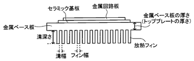
- the metal base plate has a thermal conductivity of 170 W / (m ⁇ K) or more, the metal base plate has a Vickers hardness of 20 to 40 (Hv), and the radiating fin has a width of 0.2. Is 2.0 mm, the width of the groove formed between the plurality of heat radiation fins is 0.2 to 2.0 mm, and the depth of the groove is 2 to 20 mm. , Fin integration substrate.
- the thickness of the portion of the metal base plate where the heat dissipating fins are not formed may be 0.5 to 5 mm.
- the plurality of radiating fins may be formed to protrude in a substantially vertical direction with respect to the metal base plate, and may be substantially parallel to each other.
- the metal base plate may be an aluminum alloy containing at least one element selected from Si, Mg, Zn, Bi, and Sn.
- the metal base plate may have a crystal grain size of 5 mm or less.
- the arrangement of the plurality of radiating fins may be staggered.
- a liquid-cooled jacket having a box shape in which a plurality of the heat radiation fins are accommodated may be provided, and the jacket may be joined to the metal base plate. The jacket and at least a part of the tip of the radiation fin may be joined.
- a metal circuit board made of aluminum or an aluminum alloy is joined to one surface of a ceramic substrate, and a flat metal base made of aluminum or an aluminum alloy is joined to the other surface.
- a multi-layer disk cutter is laminated on the surface where the tensile stress is applied. It is moved while rotating the cutter is formed by performing a grooving to form a plurality of grooves, the manufacturing method of the fin integration substrate.
- the metal circuit board may be integrally formed by a plate portion and a block portion protruding in the vicinity of the center of the plate portion, and a surface on the block portion on which the heat radiating fins are formed may be convex.
- the central part of the block part may be thicker than the peripheral part of the block part.
- the rotary blades of the multi-cutter may be alternating blades, and the rake angle may be 10 ° or more.
- the cutting speed of the multi-cutter may be 700 mm / min or more.
- the jig may have a shape that does not contact the ceramic substrate, and may be disposed at a position that does not interfere with the deformation of the metal base plate in the grooving process.
- the jig may be a vacuum suction method, and the suction force may be controllable.
- a box-shaped liquid-cooled jacket for housing the radiation fins may be joined to the surface of the metal base plate on which the radiation fins are formed.
- the metal base plate and the jacket may be joined by brazing. You may join the said jacket and the front-end
- a fin-integrated substrate having a fine pitch heat radiation fin in a simple process by a processing method in which warpage of the metal base plate and deformation of the heat radiation fin (occurrence of warp or the like) are suppressed.
- a method for manufacturing a fin-integrated substrate capable of supporting the above. Furthermore, with this manufacturing method, air-cooled (gas-cooled) or liquid-cooled fins that have fine pitch radiating fins and are excellent in strength, cooling efficiency, heat dissipation, electronic component assembly, thermal shock resistance and corrosion resistance An integrated substrate can be provided.
- FIG. 3 is a perspective view of a workpiece 40.
- FIG. It is explanatory drawing about grooving. It is side surface sectional drawing of the to-be-cut material 40 when the shape of the to-be-cut part 40b is made into the shape whose center part is thicker than an edge part. It is side surface sectional drawing of the to-be-cut material 40 at the time of making the to-be-cut material 40 the curved shape.
- A It is a top view of fin integrated substrate 1 '.
- (B) It is side surface sectional drawing which looked at the fin integrated substrate 1 'from the X direction in Fig.6 (a).
- FIG. 6 is a graph showing the difference in temperature of a heating element in an unsteady state when a heating element is heated under the same conditions (same heat input) in four types of metal base plates.
- FIG. 6 is a configuration explanatory view (cross-sectional view) of an apparatus used in Examples 2 to 4.
- FIG. 10 is an enlarged view of a metal base plate, a ceramic substrate, and a metal circuit board in FIG. 9. It is sectional drawing explaining the clamping method of Example 6.
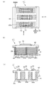
- FIG. 1A is a plan view of a fin integrated substrate 1 according to an embodiment of the present invention
- FIG. 1B is a side sectional view of the fin integrated substrate 1 according to an embodiment of the present invention.
- a metal circuit board 15 made of aluminum or an aluminum alloy is joined to the upper surface of the ceramic substrate 10 (upper in FIG. 1B).
- a metal base plate 20 made of aluminum or an aluminum alloy is joined to the lower surface of 10 (lower part in FIG. 1B).
- a plurality of heat radiation fins 20a are formed integrally with the metal base plate 20 so as to protrude substantially vertically from the lower surface of the metal base plate 20 and to be arranged substantially parallel to each other at a predetermined interval.
- the groove part 25 is formed in the gap part between the fins of the plurality of radiating fins 20a.
- the radiation fin 20a is formed near the center of the lower surface of the metal base plate 20, and the lower peripheral edge 27 of the metal base plate 20 has a planar shape.
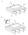
- the fin integrated substrate 1 shown in FIG. 1 is a liquid cooling type, and is formed in a bottom portion (lower side in FIG. 1B), for example, a box shape molded so as to be able to accommodate the heat radiating fins 20a.
- the liquid cooling type jacket 30 is attached by joining (for example, brazing). That is, the cooling liquid A supplied from a cooling liquid supply unit (not shown) flows inside the jacket 30 (the part in which the heat radiation fins 20a are stored). The heat radiation fins 20a are cooled by the cooling liquid A.
- the thermal conductivity of the metal base plate 20 is 170 W / (m ⁇ K) or more, and the hardness is 20 to 40 in terms of Vickers hardness Hv.
- the warp is preferably 100 ⁇ m or less.
- the peripheral edge 27 preferably has a thickness of 0.5 to 5 mm.
- warp refers to the difference in height between the center and the edge of the flat surface of the metal base plate 20 on the ceramic substrate bonding side, and the warp when the metal base plate 20 warps in a concave shape is corrected. (+), And the warp when it is warped convexly is negative (-).
- the metal base plate has a role to transmit heat of the element that generates heat on the circuit to the fin, and it is preferable that the thermal conductivity of the metal base plate is 170 W / (m ⁇ K) or more.
- the thermal conductivity of the metal base plate is 170 W / (m ⁇ K) or more.
- it is 180 W / (m ⁇ K) or more.
- the Vickers hardness of Al or Al alloy which is the material of the metal base plate
- the heat cycle resistance (described later) is significantly reduced.
- the Vickers hardness is less than 20 (Hv)
- the Vickers hardness is less than 20 (Hv)
- the heat is [holding at ⁇ 40 ° C. for 30 minutes ⁇ holding at 25 ° C. for 10 minutes ⁇ holding at 125 ° C. for 30 minutes ⁇ holding at 25 ° C. for 10 minutes ⁇ ] once.
- the cycle test thermal shock repetition test
- peripheral part thickness exceeds 5 mm, melting and joining by local heating such as laser welding becomes difficult. If the thickness is less than 0.5 mm, there is a possibility of fracture due to fatigue due to expansion / contraction when heating / cooling is repeated due to insufficient mechanical strength.
- the metal base plate 20 is preferably made of aluminum or an aluminum alloy, but more preferably an aluminum alloy containing at least one element selected from Si, Mg, Zn, Bi, and Sn.
- the crystal grain size is preferably 5 mm or less. When the crystal grain size exceeds 5 mm, the level difference and deformation of the crystal grain boundary when a heat cycle is applied increase.
- the width of the radiating fin 20a is 0.2 to 2.0 mm, more preferably 0.3 to 1.5 mm, and the groove portion 25 formed between the radiating fins 20a. Is preferably 0.2 to 2.0 mm, more preferably 0.5 to 2.0 mm, and the depth of the groove 25 is preferably 2 to 20 mm, more preferably 3 to 15 mm.
- the width of the radiating fin 20a is less than 0.2 mm, the amount of heat transfer (fin efficiency) decreases, and when it exceeds 2.0 mm, the number of fins becomes too small. Also, if the fin width is 0.2 mm or less, the material characteristics of the metal base plate of the present invention may be easily deformed even in the fin processing method. If the fin width exceeds 2 mm, the mold dimensions may be set. This is a dimensional area that can be cast.
- the width of the groove portion 25 is less than 0.2 mm, the pressure loss is remarkably increased and the cooling ability is lowered, and when it exceeds 2.0 mm, the flow velocity is significantly lowered and the cooling ability is lowered.
- the depth of the groove 25 is less than 2 mm, the pressure loss increases, and when it exceeds 20 mm, the fin integrated substrate 1 becomes thick. If the groove width (fin interval) exceeds 2 mm, it is an area that can be cast by setting the dimensions of the mold, and if the groove width is made thinner than 0.2 mm, problems such as cutting chips being easily generated during processing occur. There is a fear.
- the depth of the groove is less than 2 mm, the pressure loss becomes too large and the heat exchange rate decreases. If it is deeper than 20 mm, the flow rate becomes too small and the heat exchange rate decreases, and there is a risk that problems such as cutting chips during processing being easily clogged may occur.
- the thickness and material / composition of the metal base plate 20, the width and pitch of the radiating fins 20a are defined as described above, and the liquid cooling type
- the jacket 30 By attaching the jacket 30 so as to accommodate the heat dissipating fins 20a, the fin integrated substrate 1 having excellent strength, cooling efficiency and heat dissipating property can be obtained.
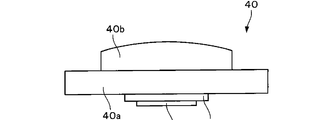
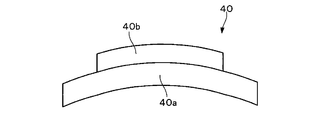
- FIG. 2 is a perspective view of the workpiece 40 that is the metal base plate 20 at the previous stage where the heat dissipating fins 20a are formed, and includes a base portion 40a and a cut portion 40b.
- the portion to be cut 40b is processed to become the heat radiation fin 20a.
- FIG. 2 is a perspective view of the workpiece 40 that is the metal base plate 20 at the previous stage where the heat dissipating fins 20a are formed, and includes a base portion 40a and a cut portion 40b.
- the portion to be cut 40b is processed to become the heat radiation fin 20a.
- FIG. 3 is explanatory drawing in the case of performing the grooving process which processes the to-be-cut material 40 and forms the radiation fin 20a.
- the heat radiating fins 20 a are illustrated as being formed in the lower part of the drawing (the lower surface of the metal base plate 20). However, in FIG. 2 and FIG. The fins 20a) are shown as facing upward in the figure, and will be described below along the arrangement of the drawings.
- the material to be cut 40 includes a substantially rectangular base portion 40a and a substantially rectangular cut portion 40b formed integrally with the base portion 40a at the center of the base portion 40a.
- the ceramic substrate 10 and the metal circuit board 15 are bonded to the lower surface of the base portion 40a (the lower surface in FIG. 2).
- the material to be cut 40 may be a single substantially rectangular shape.
- the peripheral portion may be formed by cutting or the like before or after the fin processing.
- the radiating fin 20a is formed by grooving the workpiece 40b
- the workpiece 40 is fixed by the jig 50 as shown in FIG.
- the multi-cutter 55 cuts into the cut portion 40.
- the shape of the jig 50 is such that the base portion 40a can be inserted, and the jig 50 contacts the ceramic substrate 10 bonded to the lower surface of the workpiece 40.
- the deformed cut portion 40b and the jig 50 are not in contact with each other.
- the workpiece 40 is fixed by the jig 50 so that a tensile stress is applied to the upper surface (upper surface in FIG. 3) of the cut portion 40b. That is, as shown in FIG.
- the base portion 40a is inserted into the jig 50, and for example, the tip of the screw 50 ′ is pressed so as to apply pressure to the lower side surface of the base portion 40a, so that the material 40 is cut.
- the fixing is performed in a state where a tensile stress is applied to the upper surface of the cut portion 40b.
- the multi-cutter 55 is rotated and pressed against the upper surface of the cut portion 40b to perform grooving.
- the multi-cutter 55 has a configuration in which a plurality of disk-type cutters 55 ′ are stacked so as to be parallel to each other, and the disk-type cutter 55 ′ rotates at high speed to cut an object. It is.
- the multi-cutter 55 is pressed against the cut portion 40b so that the rotation direction of the disk cutter 55 'and the longitudinal direction of the cut portion 40b are parallel, and the multi-cutter is pressed. Machining is performed by moving 55 in the longitudinal direction of the cut portion 40b.
- the depth of the groove 25 formed between the radiating fins 20a is preferably 2 to 20 mm, the cutting depth of the multi-cutter 55 with respect to the cut portion 40b is cut. Similarly, it is preferably 2 to 20 mm.
- the rotary blades of the multi-cutter 55 are alternating blades, and the rake angle is preferably 10 ° or more, and the cutting speed (moving speed during cutting) of the multi-cutter 55 is 700 mm / min or more. Is preferred.
- the cutting speed of the multi cutter 55 is more preferably 1000 mm / min or more.
- the deformation of the radiating fins 20 a formed after the grooving process is suppressed, and the jig 50 is used to cover the surface.
- the jig 50 is used to cover the surface.
- the grooving process is performed using the jig 50 in a state where a tensile stress is applied to the upper surface of the part 40b to be cut. Therefore, the shape of the non-cutting portion 40b may be thicker at the center than the end portion, as long as the occurrence of warpage of the entire workpiece 40 (metal base plate 20) can be suppressed.
- FIG. 4 is a side cross-sectional view of the material to be cut 40 when the shape of the part to be cut 40b is made thicker at the center than the end (a shape that is convex upward in FIG. 4).
- the ceramic substrate 10 and the metal circuit board 15 may be joined to the lower surface (the lower surface in FIG. 4) of the base portion 40a during the grooving process.
- the shape of the part to be cut 40b thicker at the center than at the end, the residual stress produced by the cutting after the grooving (cutting) by the multi-cutter 55 is performed,
- the shape of the cut portion 40b after grooving is flat, and the metal base plate 20 (fin integrated substrate 1) having a desired shape is manufactured.
- obtaining a preferable numerical value by performing an appropriate grooving process suitably do it.
- the depth of the groove in the central portion is increased. That is, the height of the fin increases, but the tip of the fin at this portion may be joined to the jacket in a later step.
- FIG. 5 is a side cross-sectional view of the workpiece 40 when the entire workpiece 40 is warped (convex shape upward in FIG. 5).
- the entire shape of the workpiece 40 is warped in advance so that after the grooving (cutting) by the multi-cutter 55 is performed, the residual stress generated by the cutting and the change thereof are caused by the change.
- the shape after grooving of the entire workpiece 40 including the cutting portion 40b becomes flat, and the metal base plate 20 (fin integrated substrate 1) having a desired shape is manufactured.
- the present invention is not necessarily limited to this configuration.
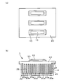
- a plurality of heat radiation fins 20 a may be formed at a plurality of locations below the metal base plate 20.
- FIG. 7 it is conceivable to integrally form a plurality of radiating fins 20 a at a plurality of staggered positions when viewed from below the metal base plate 20.
- FIGS. 6 and 7 show a fin-integrated substrate 1 ′ in which a plurality of heat radiation fins 20 a are integrally formed at a plurality of locations below the metal base plate 20 and a plurality of zigzag-shaped substrates. It is explanatory drawing of the fin integrated substrate 1 '' which is the structure formed in FIG.
- FIGS. 6A and 7A are plan views of the fin-integrated substrates 1 ′ and 1 ′′
- FIGS. 6B and 7B are FIGS. 7 (a) is a side cross-sectional view seen from the X direction (FIG. 6 (a), FIG. 7 (a) downward direction), and FIG. 6 (c) and FIG. It is side surface sectional drawing seen from the Y direction (FIG.
- the radiation fin 20a formed in the lower surface of the metal base board 20 is shown with the broken line for description.
- the radiating fins 20a are formed in three rows as viewed from the X direction in FIGS. 6A and 7A, and viewed from the X direction. First row, second row, and third row from the front side (the lower side in FIG. 6 and FIG. 7).
- a plurality of radiating fins 20 a are formed at a plurality of staggered positions when viewed from below the metal base plate 20. That is, when the fin-integrated substrate 1 ′ is viewed from the X direction (downward in FIG. 7A), the second row of radiation fins 20a can be seen from between the first row of radiation fins 20a. It has become. Further, the first row of radiation fins 20a and the third row of radiation fins 20a may be arranged so as to overlap each other when viewed from the X direction.
- the plurality of heat radiating fins may be formed discontinuously on the metal base plate, and may be formed, for example, at positions on the opposite surface of the metal base plate corresponding to the metal circuit plate.
- the radiation fin 20a is formed in several places, you may attach the jacket 30 to each.
- the liquid cooling type jacket 30 was attached so that the radiation fin 20a might be accommodated, at this time, the front-end
- air cooling gas cooling
- Example 1 As an example of the present invention, four types of metal base plates (thickness 1.0 mm, 3.0 mm, 5.0 mm, 10.0 mm) having heating elements installed on the same condition on the upper surface where only the base thickness was changed, The simulation verified the difference in temperature change of the heating element due to the difference in base thickness.
- FIG. 8 is a graph showing the difference in the temperature of the heating element in an unsteady state when the heating element is heated under the same conditions (the same heat input) in the above-described four types of metal base plates.
- the temperature of the heating element in the metal base plate having a thickness of 1.0 mm and 3.0 mm is different from the temperature of the heating element in the metal base plate having a thickness of 5.0 mm and 10.0 mm. It was found that the cooling efficiency was better when a metal base plate having a thickness of 5.0 mm or more was used. From FIG. 8 and required characteristics such as heat dissipation and strength, it was found that the optimum thickness of the metal base plate is 3.0 to 5.0 mm. From the simulation results, it was estimated that the optimum width of the radiating fin 20a at that time was 0.7 mm, the optimum width of the groove 25 was 1 to 5 mm, and the optimum depth of the groove 25 was 3.5 mm. At this time, when the thickness of the metal base plate was 5.0 mm, the estimated temperature of the element was expected to decrease by about 9% with respect to the thickness of 1.0 mm.
- FIG. 9 shows the apparatus used
- FIG. 10 shows the metal base plate, ceramic substrate and metal circuit board extracted from FIG.
- a metal circuit board having a length of 31 mm, a width of 31 mm, and a thickness of 0.6 mm is bonded to one surface of an AlN substrate having a length of 35 mm, a width of 35 mm, and a thickness of 0.6 mm, and a fin is connected to the other surface of the AlN substrate.
- a metal base plate not including the height (thickness of the top plate) having a thickness of 1 mm and a length of 69.5 mm ⁇ width of 69.5 mm was formed.
- the shape of the fin integrated with the top plate is shown below.
- the groove depth and the fin height have the same dimensions.
- the material of the metal base plate was Al and the Vickers hardness was 21 (Hv).
- the fin shape of the sample at this time is as follows, the fin was not bent, and the warp amount of the metal base plate was 100 ⁇ m or less.
- a box-shaped water-cooled jacket was joined to this with screws so as not to leak the coolant, and cooling water at 15 ° C. was allowed to flow.
- thermocouple was brought into contact with the center of the micro heater so that the temperature could be measured.
- the thermocouple was fixed with a weight. In this state, the microheater was heated at 300 W, and the temperature rise was measured. The results are as follows, and it was found that the product has sufficient heat dissipation.
- Example 3 For the measurement of the transient thermal resistance, a sample was prepared and evaluated in the same manner as in Example 2 except that power was applied to the microheater and the slope of the temperature rise between 0.05 and 0.15 seconds was obtained. The results are as follows, and it was found that the product has sufficient heat dissipation. From this result, the thermal resistance was about 4.5 (K / W).
- Example 4 A metal base plate was joined by the same method as in Example 2, and fins were processed by a multi-cutter.
- the processing speed at this time was 400 mm / min, 700 mm / min, and 1200 mm / min.
- the processing speed (cutter feed speed) was 400 mm / min, fin fining occurred and a good shape could not be obtained. Good shapes could be obtained at 700 mm / min and 1200 mm / min.
- Example 5 Three ceramic substrates of 65 mm ⁇ 35 mm were set on a carbon mold of 90 mm ⁇ 155 mm.
- the ceramic substrate has (1) AlN having a thermal conductivity of 170 W / (m ⁇ K) and a thickness of 0.635 mm, and (2) Si 3 N 4 having a thermal conductivity of 70 W / (m ⁇ K) and a thickness of 0.32 mm. (3) Three types of Al 2 O 3 having a thermal conductivity of 20 W / (m ⁇ K) and a thickness of 0.38 mm were carried out. This carbon mold was put into a furnace at 630 ° C. in a nitrogen atmosphere.
- the carbon mold is preliminarily provided with a gap (space) of the circuit part, base plate part, and fin block part (peripheral taper 2 °), and a molten metal of Al or Al alloy is poured into the gap for joining and solidification.
- the material of the Al or Al alloy molten metal is (4) pure aluminum (Al: 99.9 mass% or more) with a thermal conductivity of 210 W / (m ⁇ K) as Al, and (5) thermal conductivity as an Al alloy.
- Two types of alloys of Al-0.5 mass% Si-0.05 mass% B having a rate of 190 W / (m ⁇ K) and a Vickers hardness of 28 were used.
- the heat sink fin was machined.
- the fin width was 1 mm
- the groove width was 0.9 mm
- the processing pitch was 1.9 mm
- the depth was 6 mm.
- a high-speed metal saw having 38 blades with a blade edge of 0.9 mm in thickness was used, and the rotation speed was 5000 rpm and the cutting speed was 1200 mm / min. Processed with one pass and degreased after processing. At this time, in any of the samples, there was no crack in the formed fin.
- fins were bent by pressing only every other row of fins using a skewer mold. To make a staggered arrangement.
- a UV curable resist ink having a circuit pattern shape was screen-printed on the circuit portion, and after UV curing, unnecessary portions in the circuit portion were removed by etching with an iron chloride solution, and the resist ink was peeled off to form a circuit pattern. Then, double zincate treatment was performed so that only the circuit pattern aluminum part was in contact with the liquid, and electric Ni plating was performed so that the film thickness averaged 5 ⁇ m.
- the flatness of the base plate was 100 ⁇ m or less, and the flatness of the circuit portion was 100 ⁇ m or less.
- the cooling case was attached by the following two methods. (8) Using an Al—Si—Mg brazing material, a cooling case made of A1050 was brazed at 600 ° C. in the atmosphere. (9) Screwed to the integrated substrate and the cooling case made of A1050 through an O-ring.
- the fin integrated substrate manufactured as described above was evaluated for heat dissipation, reliability, and corrosion resistance.
- cooling water at 25 ° C. was flowed at 10 L / min, a heater assumed to be an element was placed on the circuit pattern, and the saturation thermal resistance was measured.
- the ceramic substrate is (1), (2), the material (4) or (5) of the molten Al, presence or absence of offset press processing (6) or (7), mounting method of the cooling case (8) or (9 ) was about 0.25 K / W.
- a liquid bath (liquid phase) heat cycle test was performed in which one cycle was held at ⁇ 40 ° C. for 5 minutes and held at 125 ° C. for 5 minutes.
- the ceramic had no crack after 3000 times of the liquid bath heat cycle test, and passed the withstand voltage test of AC 9 kV in the front and back oil.
- the sample with the ceramic substrate (3) there was no crack in the ceramic after 300 times of the liquid bath heat cycle test, and the dielectric strength test of AC 5 kV in front and back oil was passed.
- the fatigue fracture of the aluminum under the ceramic after 3000 times of the liquid bath heat cycle was 2 mm or less from the creeping surface.
- Corrosion resistance evaluation was 5000 h, 50% LLC (75 ° C.), and pitting corrosion was investigated, but pitting corrosion was not confirmed in all types. The results are shown in Table 1.
- an AlN ceramic having a size of 30 mm ⁇ 30 mm ⁇ 0.64 mm, a metal base plate (substantially rectangular shaped base body and a substantially rectangular substrate integrally formed with the base portion at the center portion of the base portion).
- a material to be cut consisting of a cutting part
- a test body in which the base part was 70 mm ⁇ 70 mm ⁇ 7 mm and the cutting part was 60 mm ⁇ 60 mm ⁇ 6 mm in aluminum was produced by a casting method. Further, a test body having the same shape as the test body except that the metal base plate is only the base part (no part to be cut) was produced by the same method as the casting method.
- Samples 31 and 32 and Comparative Examples 1 and 2 which are examples of the present invention described below.
- the fin width was 1 mm
- the groove width was 0.9 mm
- the processing pitch was 1.9 mm
- the depth was 6 mm.
- a high-speed metal saw having 35 blades with a blade edge of 0.9 mm thickness, it was processed at a rotational speed of 5000 rpm and a cutting speed of 1200 mm / min.
- Samples 31 and 32 and Comparative Example 2 were used for the fin processing, and the test body consisting of a part to be cut and a base part was used for the fin processing.
- FIG. 11A shows a method of clamping the sample 31.
- FIG. 11B shows a method of clamping the sample 32. In this case, since the cutting can be performed while correcting with the tensile force, the flatness of the heat radiation fin can be improved.
- FIG. 11 (d) shows the comparative example 2, and if it changes to the clamp 62 from upper direction instead of the horizontal pressing clamp like (c), it can cut without a problem.
- the flatness of the radiating fin after cutting is affected by the flatness at the time of casting, and the fins may be warped, so care must be taken.
- cutting resistance may increase.
- the present invention is applied to a metal-ceramic bonding substrate, and in particular, a metal circuit board and a metal base plate made of aluminum or an aluminum alloy are bonded to both surfaces of the ceramic substrate, respectively.
- the present invention is applied to a fin-integrated substrate in which plate-like radiating fins that protrude and extend at a predetermined interval are formed integrally with a metal base plate and a method for manufacturing the same.
Landscapes
- Engineering & Computer Science (AREA)
- Microelectronics & Electronic Packaging (AREA)
- Condensed Matter Physics & Semiconductors (AREA)
- General Physics & Mathematics (AREA)
- Computer Hardware Design (AREA)
- Physics & Mathematics (AREA)
- Power Engineering (AREA)
- Chemical & Material Sciences (AREA)
- Manufacturing & Machinery (AREA)
- Ceramic Engineering (AREA)
- Materials Engineering (AREA)
- Cooling Or The Like Of Semiconductors Or Solid State Devices (AREA)
- Cooling Or The Like Of Electrical Apparatus (AREA)
- Ceramic Products (AREA)
Abstract
Description
本発明の実施例として、ベース厚のみを変更した上面に発熱素子を同条件で設置した4種類の金属ベース板(厚さ1.0mm、3.0mm、5.0mm、10.0mm)について、ベース厚の違いによる発熱素子の温度変化の違いについてシミュレーションによる検証を行った。
次にサンプル1~5のフィン一体基板を前述の方法で作成し、熱特性を測定した。ここで、用いた装置を図9に示し、図9中の金属ベース板、セラミック基板および金属回路板を抜き出したものが図10である。長さ35mm×幅35mm×厚さ0.6mmのAlN基板の一方の面に長さ31mm×幅31mm×厚さ0.6mmの金属回路板を接合し、前記AlN基板の他方の面にフィンの高さを含まない金属ベース板の厚さ(トッププレートの厚さ)が1mmで長さ69.5mm×幅69.5mmのものを形成した。また、トッププレートと一体となっているフィンの形状は下記に示す。なお、溝深さとフィンの高さは同一寸法である。
金属ベース板の材質はAlでビッカース硬度は21(Hv)であった。
この時のサンプルのフィン形状は以下の通りであり、フィンのビレの発生はなく、金属ベース板の反り量も100μm以下であった。
これに箱型の水冷ジャケットを冷却液がもれないようにネジ止めにより接合し、15℃の冷却水を流した。
放熱性の評価は、前記回路板表面に長さ5mm×幅5mmのマイクロヒーターを厚み10μmのシルバーグリース(9W/(m・K))を介して接触させた。また、マイクロヒーターの中央部に熱電対を接触させて温度を測定できるようにした。なお、熱電対はおもりで固定した。この状態で、マイクロヒーターを300Wで発熱させその温度上昇を測定した。その結果は以下の通りで、充分な放熱性を有することがわかった。
(サンプル形状)
溝幅 フィン幅 溝深さ 溝の数 フィンの表面積
mm mm mm mm2
サンプル1: 0.8 0.8 6 19 7,980
サンプル2: 1 0.6 5 21 7,350
サンプル3: 1 0.6 6 21 8,820
サンプル4: 1 0.6 7 21 10,290
サンプル5: 1 0.4 7 24 11,760
(放熱性測定結果1)
飽和熱抵抗(℃) 過渡熱抵抗(℃/sec)
サンプル1: 58.2 58.0
サンプル2: 57.0 58.1
サンプル3: 56.9 58.0
サンプル4: 56.8 58.4
サンプル5: 57.6 57.7
飽和熱抵抗はマイクロヒーターに電力を加えて2分後の温度を測定したもの。
過渡熱抵抗は、マイクロヒーターに電力を加えて0.1~0.4秒の間の温度上昇の傾きを求めたもの。
過渡熱抵抗の測定について、マイクロヒーターに電力を加えて0.05~0.15秒の間の温度上昇の傾きを求めた以外は、実施例2と同様にサンプルを作成し、評価した。その結果は以下の通りで、充分な放熱性を有することがわかった。
この結果より熱抵抗は約4.5(K/W)であった。
(サンプル形状)
溝幅 フィン幅 溝深さ 溝の数 フィンの表面積
mm mm mm mm2
サンプル6: 0.8 0.8 6 19 7,980
サンプル7: 1 0.4 7 24 11,760
(放熱性測定結果1)
飽和熱抵抗(℃) 過渡熱抵抗(℃/sec)
サンプル6: 61.3 76.2
サンプル7: 62.3 80.1
実施例2と同様の方法で金属ベース板を接合し、マルチカッターによりフィンの加工を行った。このときの加工速度を400mm/min、700mm/min、1200mm/minとした。加工速度(カッターの送り速度)が400mm/minのとき、フィンのビレが発生して良好な形状を得ることができなかった。700mm/min、1200mm/minでは良好な形状を得ることができた。
90mm×155mmのカーボン型に、65mm×35mmの3枚のセラミックス基板をセットした。セラミックス基板は、(1)熱伝導率170W/(m・K)、厚さ0.635mmのAlN、(2)熱伝導率70W/(m・K)、厚さ0.32mmのSi3N4、(3)熱伝導率が20W/(m・K)、厚さ0.38mmのAl2O3の3種類について実施した。このカーボン型を、630℃の窒素雰囲気の炉に投入した。カーボン型には、予め、回路部、ベース板部、フィンブロック部(外周のテーパー2°)の空隙(空間)が設けられており、この空隙にAl又はAl合金の溶湯を流し込み、接合、凝固させた。Al又はAl合金溶湯の材質は、(4)Alとして熱伝導率210W/(m・K)、ビッカース硬度24の純アルミニウム(Al:99.9質量%以上)、(5)Al合金として熱伝導率190W/(m・K)、ビッカース硬度28のAl-0.5質量%Si-0.05質量%B合金の2種類とした。

セラミックス基板として、30mm×30mm×0.64mmの大きさのAlNセラミックス、金属ベース板(略矩形状のベース部とベース部の中央部にベース部と一体的に構成されている略矩形状の被切削部からなる被切削材)として、ベース部が70mm×70mm×7mm、被切削部が60mm×60mm×6mmの大きさのアルミとした試験体を鋳造法で作製した。また、金属ベース板がベース部のみである(被切削部がない)以外は前記試験体と同様の形状である試験体を、前記鋳造法と同様の方法で作製した。
Claims (19)
- セラミックス基板の一方の面にアルミニウムまたはアルミニウム合金からなる金属回路板が接合されると共に、他方の面にアルミニウムまたはアルミニウム合金からなる平板状の金属ベース板の一方の面が接合され、前記金属ベース板の他方の面から突出して互いに所定の間隔で配置するように複数の放熱フィンが前記金属ベース板と一体的に形成されたフィン一体型基板において、
前記金属ベース板の熱伝導率が170W/(m・K)以上であり、
前記金属ベース板の硬度がビッカース硬度で20~40(Hv)であり、
前記放熱フィンの幅が0.2~2.0mmであり、
複数の前記放熱フィン同士の間に形成される溝部の幅が0.2~2.0mmであり、
前記溝部の深さが2~20mmである、フィン一体型基板。 - 前記金属ベース板の前記放熱フィンが形成されていない部分の厚さが0.5~5mmである、請求項1に記載のフィン一体型基板。
- 複数の前記放熱フィンは前記金属ベース板に対して略垂直方向に突出するように形成され、かつ、互いに略平行である、請求項1に記載のフィン一体型基板。
- 前記金属ベース板はSi、Mg、Zn、Bi、Snから選ばれる少なくとも1つの元素を含有するアルミニウム合金である、請求項1に記載のフィン一体型基板。
- 前記金属ベース板の結晶粒径は5mm以下である、請求項1に記載のフィン一体型基板。
- 複数の前記放熱フィンの配置は千鳥状である、請求項1に記載のフィン一体型基板。
- 複数の前記放熱フィンが収納される箱型形状の液冷式のジャケットを備え、前記ジャケットは前記金属ベース板に接合される、請求項1に記載のフィン一体型基板。
- 前記ジャケットと少なくとも一部の前記放熱フィンの先端部が接合されている、請求項7に記載のフィン一体型基板。
- セラミックス基板の一方の面にアルミニウムまたはアルミニウム合金からなる金属回路板が接合されると共に、他方の面にアルミニウムまたはアルミニウム合金からなる平板状の金属ベース板の一方の面が接合され、前記金属ベース板の他方の面から突出して互いに所定の間隔で配置するように複数の放熱フィンが前記金属ベース板と一体的に形成されたフィン一体型基板を製造するフィン一体型基板の製造方法であって、
前記金属回路板の前記セラミックス基板との接合は溶湯接合法によって行われ、
前記金属ベース板の一部である被切削部への複数の放熱フィンの形成は、前記被切削部の放熱フィンを形成させる面に引張応力を負荷させるように治具による固定を行い、引張応力が負荷された面上に複数枚の円盤型カッターを積層したマルチカッターを回転させながら移動させて複数の溝を形成させる溝入れ加工を行うことで形成される、フィン一体型基板の製造方法。 - 前記金属回路板は、板部およびその板部中央近傍において突出するブロック部によって一体的に構成され、前記放熱フィンを形成させる前記ブロック部上の面は凸形状である、請求項9に記載のフィン一体型基板の製造方法。
- 前記ブロック部の中央部は、前記ブロック部の周縁部より厚い、請求項10に記載のフィン一体型基板の製造方法。
- 前記マルチカッターの回転刃は交互刃であり、かつすくい角が10°以上である、請求項9に記載のフィン一体型基板の製造方法。
- 前記マルチカッターの切削スピードは700mm/min以上である、請求項9に記載のフィン一体型基板の製造方法。
- 前記治具は前記セラミックス基板に非接触な形状であり、かつ、前記溝入れ加工における金属ベース板の変形に非干渉な位置に配置される、請求項9に記載のフィン一体型基板の製造方法。
- 前記治具は真空吸引方式であり、その吸引力は制御可能である、請求項9に記載のフィン一体型基板の製造方法。
- 前記溝入れ加工後に、放熱フィンが形成された前記金属ベース板の面上に、前記放熱フィンを収納する箱型形状の液冷式のジャケットを接合する、請求項9に記載のフィン一体型基板の製造方法。
- 前記金属ベース板と前記ジャケットの接合がろう接である、請求項16に記載のフィン一体型基板の製造方法。
- 前記放熱フィンの少なくとも一部の先端部と前記ジャケットを接合する、請求項16に記載のフィン一体型基板の製造方法。
- 前記ジャケットにおいて、前記放熱フィン先端部と前記ジャケットの接合が行われる部分は、他の部分に比べ薄肉化されている、請求項16に記載のフィン一体型基板の製造方法。
Priority Applications (5)
| Application Number | Priority Date | Filing Date | Title |
|---|---|---|---|
| RU2012134375/28A RU2521787C2 (ru) | 2010-01-12 | 2011-01-12 | Реберная объединенная подложка и способ изготовления реберной объединенной подложки |
| CN201180005825.7A CN102714929B (zh) | 2010-01-12 | 2011-01-12 | 翅片一体型基板及翅片一体型基板的制造方法 |
| KR1020127018072A KR101690825B1 (ko) | 2010-01-12 | 2011-01-12 | 핀 일체형 기판 및 핀 일체형 기판의 제조 방법 |
| US13/521,922 US8927873B2 (en) | 2010-01-12 | 2011-01-12 | Fin-integrated substrate and manufacturing method of fin-integrated substrate |
| EP11732898.9A EP2525638B1 (en) | 2010-01-12 | 2011-01-12 | Method of manufacturing a substrate with integrated fins |
Applications Claiming Priority (4)
| Application Number | Priority Date | Filing Date | Title |
|---|---|---|---|
| JP2010-003630 | 2010-01-12 | ||
| JP2010003630 | 2010-01-12 | ||
| JP2011-000386 | 2011-01-05 | ||
| JP2011000386A JP5686606B2 (ja) | 2010-01-12 | 2011-01-05 | フィン一体型基板の製造方法およびフィン一体型基板 |
Publications (1)
| Publication Number | Publication Date |
|---|---|
| WO2011087028A1 true WO2011087028A1 (ja) | 2011-07-21 |
Family
ID=44304301
Family Applications (1)
| Application Number | Title | Priority Date | Filing Date |
|---|---|---|---|
| PCT/JP2011/050381 WO2011087028A1 (ja) | 2010-01-12 | 2011-01-12 | フィン一体型基板およびフィン一体型基板の製造方法 |
Country Status (7)
| Country | Link |
|---|---|
| US (1) | US8927873B2 (ja) |
| EP (1) | EP2525638B1 (ja) |
| JP (1) | JP5686606B2 (ja) |
| KR (1) | KR101690825B1 (ja) |
| CN (1) | CN102714929B (ja) |
| RU (1) | RU2521787C2 (ja) |
| WO (1) | WO2011087028A1 (ja) |
Cited By (6)
| Publication number | Priority date | Publication date | Assignee | Title |
|---|---|---|---|---|
| FR2978872A1 (fr) * | 2011-08-01 | 2013-02-08 | Valeo Sys Controle Moteur Sas | Dispositif comportant un substrat portant au moins un composant electronique et une piece dans laquelle est menage un espace interieur apte a recevoir un fluide de refroidissement |
| WO2013068009A1 (en) * | 2011-11-09 | 2013-05-16 | Danfoss A/S | Power module cooling |
| WO2015033724A1 (ja) * | 2013-09-05 | 2015-03-12 | 富士電機株式会社 | 電力用半導体モジュール |
| JP2016219571A (ja) * | 2015-05-19 | 2016-12-22 | 昭和電工株式会社 | 液冷式冷却装置 |
| JP2018098469A (ja) * | 2016-12-16 | 2018-06-21 | 三菱アルミニウム株式会社 | 空冷モジュール |
| WO2023053580A1 (ja) * | 2021-09-28 | 2023-04-06 | 日軽熱交株式会社 | パワーデバイス用冷却器 |
Families Citing this family (35)
| Publication number | Priority date | Publication date | Assignee | Title |
|---|---|---|---|---|
| JP6012990B2 (ja) * | 2012-03-19 | 2016-10-25 | 日本軽金属株式会社 | 放熱器一体型基板の製造方法 |
| JP6262422B2 (ja) * | 2012-10-02 | 2018-01-17 | 昭和電工株式会社 | 冷却装置および半導体装置 |
| JP5838949B2 (ja) * | 2012-10-17 | 2016-01-06 | 日本軽金属株式会社 | 複合型中空容器の製造方法及び複合型中空容器 |
| ITBO20120618A1 (it) * | 2012-11-09 | 2014-05-10 | Mecc Al S R L A Socio Unico | Procedimento per la realizzazione di un dissipatore e dissipatore cosi' ottenuto |
| KR101446023B1 (ko) | 2013-05-28 | 2014-10-01 | 전북대학교산학협력단 | 히트싱크 |
| CN107517596B (zh) * | 2015-03-25 | 2019-11-26 | 三菱电机株式会社 | 电力转换装置 |
| WO2016158020A1 (ja) * | 2015-04-01 | 2016-10-06 | 富士電機株式会社 | 半導体モジュール |
| JP6558114B2 (ja) | 2015-07-16 | 2019-08-14 | 富士通株式会社 | 冷却部品の接合方法 |
| KR101703724B1 (ko) | 2015-12-09 | 2017-02-07 | 현대오트론 주식회사 | 파워 모듈 패키지 |
| CN112714588A (zh) * | 2015-12-30 | 2021-04-27 | 讯凯国际股份有限公司 | 热交换腔及液冷装置 |
| JP6462958B2 (ja) * | 2016-06-16 | 2019-01-30 | 三菱電機株式会社 | 半導体実装用放熱ベース板およびその製造方法 |
| CN108231714B (zh) * | 2016-12-14 | 2019-12-27 | 株洲中车时代电气股份有限公司 | 一种功率模块及其制作方法 |
| JP2018163995A (ja) * | 2017-03-27 | 2018-10-18 | 三菱電機株式会社 | 半導体実装用放熱ベース板及びその製造方法並びに製造装置 |
| US10211124B2 (en) * | 2017-05-12 | 2019-02-19 | Intel Corporation | Heat spreaders with staggered fins |
| JP6940997B2 (ja) * | 2017-07-31 | 2021-09-29 | Dowaメタルテック株式会社 | アルミニウム−セラミックス接合基板およびその製造方法 |
| US10292316B2 (en) * | 2017-09-08 | 2019-05-14 | Hamilton Sundstrand Corporation | Power module with integrated liquid cooling |
| JP6939481B2 (ja) * | 2017-11-30 | 2021-09-22 | 富士通株式会社 | 冷却ジャケット及び電子機器 |
| CN108337862B (zh) * | 2018-03-02 | 2019-09-06 | 惠州市博宇科技有限公司 | 一种新能源电动车专用铝基板 |
| US10900412B2 (en) * | 2018-05-31 | 2021-01-26 | Borg Warner Inc. | Electronics assembly having a heat sink and an electrical insulator directly bonded to the heat sink |
| CN108770304A (zh) * | 2018-06-27 | 2018-11-06 | 江苏英杰电子器件有限公司 | 一种分体式散热器盖板 |
| EP3595002A1 (de) | 2018-07-12 | 2020-01-15 | Heraeus Deutschland GmbH & Co KG | Metall-keramik-substrat mit einer zur direkten kühlung geformten folie als substratunterseite |
| CN110828398A (zh) * | 2018-08-08 | 2020-02-21 | 株洲中车时代电气股份有限公司 | 用于功率半导体模块封装的一体化均热基板及其制造方法 |
| JP7334464B2 (ja) | 2019-05-15 | 2023-08-29 | 富士電機株式会社 | 半導体モジュール、半導体モジュールの製造方法および段差冶具 |
| CN113892172B (zh) * | 2019-05-30 | 2025-01-14 | 三菱电机株式会社 | 半导体装置 |
| JP7388145B2 (ja) * | 2019-11-19 | 2023-11-29 | 株式会社レゾナック | 半導体冷却装置 |
| DE102019135146B4 (de) * | 2019-12-19 | 2022-11-24 | Rogers Germany Gmbh | Metall-Keramik-Substrat |
| CN114365282A (zh) * | 2020-03-18 | 2022-04-15 | 富士电机株式会社 | 半导体模块 |
| JP7383582B2 (ja) * | 2020-07-29 | 2023-11-20 | Dowaメタルテック株式会社 | アルミニウム-セラミックス接合基板およびその製造方法 |
| CN112144054B (zh) * | 2020-08-27 | 2022-12-13 | 东南大学 | 带有鳍式散热片的激光熔覆冷却装置 |
| CN112285974B (zh) * | 2020-10-30 | 2021-12-03 | 惠州市华星光电技术有限公司 | 背光模组和显示装置 |
| JP7622410B2 (ja) * | 2020-12-01 | 2025-01-28 | 富士電機株式会社 | 冷却器及び半導体装置 |
| JP7555261B2 (ja) * | 2020-12-22 | 2024-09-24 | 日立Astemo株式会社 | 電気回路体および電力変換装置 |
| DE102021201263A1 (de) * | 2021-02-10 | 2022-08-11 | Zf Friedrichshafen Ag | Leistungsmodul zum Betreiben eines Elektrofahrzeugantriebs mit einer Direktkühlung der Leistungshalbleiter |
| CN114126345B (zh) * | 2021-10-18 | 2022-07-05 | 富贤勋电子科技(南通)有限公司 | 一种散热片的制作方法 |
| CN114850797B (zh) * | 2022-05-18 | 2023-11-03 | 浙江华鑫实业有限公司 | 一种通信用散热器加工方法 |
Citations (8)
| Publication number | Priority date | Publication date | Assignee | Title |
|---|---|---|---|---|
| JP2002185175A (ja) * | 2000-12-19 | 2002-06-28 | Toyota Motor Corp | 冷却フィン装置及び機器 |
| JP2004022914A (ja) * | 2002-06-19 | 2004-01-22 | Hitachi Ltd | 絶縁回路基板とその冷却構造及ぴパワー半導体装置とその冷却構造 |
| JP2004115337A (ja) * | 2002-09-27 | 2004-04-15 | Dowa Mining Co Ltd | アルミニウム−セラミックス接合体 |
| JP2006245479A (ja) * | 2005-03-07 | 2006-09-14 | Nichicon Corp | 電子部品冷却装置 |
| JP2006324647A (ja) | 2005-04-21 | 2006-11-30 | Nippon Light Metal Co Ltd | 液冷ジャケット |
| JP2008135757A (ja) | 2005-04-21 | 2008-06-12 | Nippon Light Metal Co Ltd | 液冷ジャケット |
| JP2008218938A (ja) | 2007-03-08 | 2008-09-18 | Dowa Metaltech Kk | 金属−セラミックス接合基板 |
| JP2009056520A (ja) | 2007-08-30 | 2009-03-19 | Nippon Light Metal Co Ltd | 溝入れ加工方法 |
Family Cites Families (16)
| Publication number | Priority date | Publication date | Assignee | Title |
|---|---|---|---|---|
| SU1450154A1 (ru) * | 1986-05-11 | 1989-01-07 | Предприятие П/Я В-2634 | Радиоэлектронный модуль |
| DE19615787A1 (de) * | 1996-04-20 | 1997-10-23 | Bosch Gmbh Robert | Verfahren zur Herstellung eines keramischen Multilayer-Substrats |
| JP2002083910A (ja) * | 2000-09-08 | 2002-03-22 | Mizutani Denki Kogyo Kk | 電子部品の放熱器およびその製造方法 |
| US6845647B2 (en) * | 2002-08-28 | 2005-01-25 | Fan Zhen Co., Ltd. | Heat sink processing method |
| JP4115795B2 (ja) * | 2002-09-27 | 2008-07-09 | 株式会社東芝 | 帳票類処理装置 |
| US7215545B1 (en) * | 2003-05-01 | 2007-05-08 | Saeed Moghaddam | Liquid cooled diamond bearing heat sink |
| JP2005011922A (ja) * | 2003-06-18 | 2005-01-13 | Mitsubishi Electric Corp | ヒートシンクを備えた両面銅貼り基板、およびこれを用いた半導体装置 |
| JP4821013B2 (ja) * | 2003-09-29 | 2011-11-24 | Dowaメタルテック株式会社 | アルミニウム−セラミックス接合基板およびその製造方法 |
| EP1518847B1 (en) * | 2003-09-29 | 2013-08-28 | Dowa Metaltech Co., Ltd. | Aluminum/ceramic bonding substrate and method for producing same |
| JP4543279B2 (ja) * | 2004-03-31 | 2010-09-15 | Dowaメタルテック株式会社 | アルミニウム接合部材の製造方法 |
| JP2007294891A (ja) * | 2006-03-30 | 2007-11-08 | Dowa Metaltech Kk | 放熱器 |
| WO2007142261A1 (ja) * | 2006-06-06 | 2007-12-13 | Mitsubishi Materials Corporation | パワー素子搭載用基板、その製造方法、パワー素子搭載用ユニット、その製造方法、およびパワーモジュール |
| JP2008124187A (ja) * | 2006-11-10 | 2008-05-29 | Toyota Industries Corp | パワーモジュール用ベース |
| US7564129B2 (en) * | 2007-03-30 | 2009-07-21 | Nichicon Corporation | Power semiconductor module, and power semiconductor device having the module mounted therein |
| JP5467407B2 (ja) * | 2007-10-22 | 2014-04-09 | Dowaメタルテック株式会社 | アルミニウム−セラミックス接合体 |
| JP5381561B2 (ja) * | 2008-11-28 | 2014-01-08 | 富士電機株式会社 | 半導体冷却装置 |
-
2011
- 2011-01-05 JP JP2011000386A patent/JP5686606B2/ja active Active
- 2011-01-12 WO PCT/JP2011/050381 patent/WO2011087028A1/ja active Application Filing
- 2011-01-12 EP EP11732898.9A patent/EP2525638B1/en active Active
- 2011-01-12 CN CN201180005825.7A patent/CN102714929B/zh active Active
- 2011-01-12 KR KR1020127018072A patent/KR101690825B1/ko active Active
- 2011-01-12 US US13/521,922 patent/US8927873B2/en active Active
- 2011-01-12 RU RU2012134375/28A patent/RU2521787C2/ru active
Patent Citations (8)
| Publication number | Priority date | Publication date | Assignee | Title |
|---|---|---|---|---|
| JP2002185175A (ja) * | 2000-12-19 | 2002-06-28 | Toyota Motor Corp | 冷却フィン装置及び機器 |
| JP2004022914A (ja) * | 2002-06-19 | 2004-01-22 | Hitachi Ltd | 絶縁回路基板とその冷却構造及ぴパワー半導体装置とその冷却構造 |
| JP2004115337A (ja) * | 2002-09-27 | 2004-04-15 | Dowa Mining Co Ltd | アルミニウム−セラミックス接合体 |
| JP2006245479A (ja) * | 2005-03-07 | 2006-09-14 | Nichicon Corp | 電子部品冷却装置 |
| JP2006324647A (ja) | 2005-04-21 | 2006-11-30 | Nippon Light Metal Co Ltd | 液冷ジャケット |
| JP2008135757A (ja) | 2005-04-21 | 2008-06-12 | Nippon Light Metal Co Ltd | 液冷ジャケット |
| JP2008218938A (ja) | 2007-03-08 | 2008-09-18 | Dowa Metaltech Kk | 金属−セラミックス接合基板 |
| JP2009056520A (ja) | 2007-08-30 | 2009-03-19 | Nippon Light Metal Co Ltd | 溝入れ加工方法 |
Non-Patent Citations (1)
| Title |
|---|
| See also references of EP2525638A4 |
Cited By (8)
| Publication number | Priority date | Publication date | Assignee | Title |
|---|---|---|---|---|
| FR2978872A1 (fr) * | 2011-08-01 | 2013-02-08 | Valeo Sys Controle Moteur Sas | Dispositif comportant un substrat portant au moins un composant electronique et une piece dans laquelle est menage un espace interieur apte a recevoir un fluide de refroidissement |
| WO2013068009A1 (en) * | 2011-11-09 | 2013-05-16 | Danfoss A/S | Power module cooling |
| WO2015033724A1 (ja) * | 2013-09-05 | 2015-03-12 | 富士電機株式会社 | 電力用半導体モジュール |
| JPWO2015033724A1 (ja) * | 2013-09-05 | 2017-03-02 | 富士電機株式会社 | 電力用半導体モジュール |
| US9888611B2 (en) | 2013-09-05 | 2018-02-06 | Fuji Electric Co., Ltd. | Power semiconductor module |
| JP2016219571A (ja) * | 2015-05-19 | 2016-12-22 | 昭和電工株式会社 | 液冷式冷却装置 |
| JP2018098469A (ja) * | 2016-12-16 | 2018-06-21 | 三菱アルミニウム株式会社 | 空冷モジュール |
| WO2023053580A1 (ja) * | 2021-09-28 | 2023-04-06 | 日軽熱交株式会社 | パワーデバイス用冷却器 |
Also Published As
| Publication number | Publication date |
|---|---|
| EP2525638B1 (en) | 2021-12-08 |
| CN102714929A (zh) | 2012-10-03 |
| RU2012134375A (ru) | 2014-02-20 |
| US8927873B2 (en) | 2015-01-06 |
| CN102714929B (zh) | 2015-05-20 |
| US20120279761A1 (en) | 2012-11-08 |
| KR20130000372A (ko) | 2013-01-02 |
| KR101690825B1 (ko) | 2017-01-09 |
| EP2525638A1 (en) | 2012-11-21 |
| JP2011166122A (ja) | 2011-08-25 |
| EP2525638A4 (en) | 2013-09-04 |
| RU2521787C2 (ru) | 2014-07-10 |
| JP5686606B2 (ja) | 2015-03-18 |
Similar Documents
| Publication | Publication Date | Title |
|---|---|---|
| JP5686606B2 (ja) | フィン一体型基板の製造方法およびフィン一体型基板 | |
| JP5144279B2 (ja) | アルミニウム−炭化珪素質複合体及びそれを用いた放熱部品 | |
| EP3057125B1 (en) | Substrate for heat sink-equipped power module, and production method for same | |
| KR102027615B1 (ko) | 히트 싱크 장착 파워 모듈용 기판, 냉각기 장착 파워 모듈용 기판 및 파워 모듈 | |
| TWI550790B (zh) | 電源模組用基板、附散熱塊之電源模組用基板、電源模組、及電源模組用基板之製造方法 | |
| JP2004115337A (ja) | アルミニウム−セラミックス接合体 | |
| JP5125241B2 (ja) | パワーモジュール用基板の製造方法 | |
| JP2008227336A (ja) | 半導体モジュール、これに用いられる回路基板 | |
| JP3922538B2 (ja) | セラミックス回路基板の製造方法 | |
| JPWO2011065457A1 (ja) | 積層材およびその製造方法 | |
| JP2008218938A (ja) | 金属−セラミックス接合基板 | |
| KR20140012738A (ko) | 금속-세라믹스 접합 기판 및 그 제조 방법 | |
| JP4864593B2 (ja) | アルミニウム−炭化珪素質複合体の製造方法 | |
| JP5741793B2 (ja) | パワーモジュール用基板、ヒートシンク付パワーモジュール用基板、パワーモジュール、パワーモジュール用基板の製造方法及びヒートシンク付パワーモジュール用基板の製造方法 | |
| JP2005011922A (ja) | ヒートシンクを備えた両面銅貼り基板、およびこれを用いた半導体装置 | |
| JP5467407B2 (ja) | アルミニウム−セラミックス接合体 | |
| JP2011230954A (ja) | セラミック部材とフィン付き放熱部材との接合体の製造方法 | |
| JP6360722B2 (ja) | くし歯形放熱ピン部材を用いたパワー半導体の水冷用ピン付き放熱板 | |
| JP5631446B2 (ja) | 金属−セラミックス接合基板の製造方法 | |
| JP5724273B2 (ja) | パワーモジュール用基板、ヒートシンク付パワーモジュール用基板、パワーモジュール、パワーモジュール用基板の製造方法及びヒートシンク付パワーモジュール用基板の製造方法 | |
| JP4798171B2 (ja) | パワーモジュール用基板、パワーモジュール及びパワーモジュール用基板の製造方法 | |
| JP2017224748A (ja) | 回路基板付きヒートシンク及びその製造方法 | |
| JP2016048789A (ja) | アルミニウム−セラミックス接合体の製造方法 | |
| WO2022209024A1 (ja) | 金属-セラミックス接合基板およびその製造方法 | |
| JP2022171241A (ja) | 金属-セラミックス接合基板およびその製造方法 |
Legal Events
| Date | Code | Title | Description |
|---|---|---|---|
| WWE | Wipo information: entry into national phase |
Ref document number: 201180005825.7 Country of ref document: CN |
|
| ENP | Entry into the national phase |
Ref document number: 20127018072 Country of ref document: KR Kind code of ref document: A |
|
| NENP | Non-entry into the national phase |
Ref country code: DE |
|
| WWE | Wipo information: entry into national phase |
Ref document number: 13521922 Country of ref document: US Ref document number: 6172/DELNP/2012 Country of ref document: IN |
|
| WWE | Wipo information: entry into national phase |
Ref document number: 2011732898 Country of ref document: EP |
|
| WWE | Wipo information: entry into national phase |
Ref document number: 2012134375 Country of ref document: RU |