WO2011083758A1 - 増幅装置 - Google Patents
増幅装置 Download PDFInfo
- Publication number
- WO2011083758A1 WO2011083758A1 PCT/JP2011/000013 JP2011000013W WO2011083758A1 WO 2011083758 A1 WO2011083758 A1 WO 2011083758A1 JP 2011000013 W JP2011000013 W JP 2011000013W WO 2011083758 A1 WO2011083758 A1 WO 2011083758A1
- Authority
- WO
- WIPO (PCT)
- Prior art keywords
- power supply
- signal
- supply voltage
- voltage control
- unit
- Prior art date
Links
- 230000005236 sound signal Effects 0.000 claims abstract description 52
- 230000003321 amplification Effects 0.000 description 20
- 238000000034 method Methods 0.000 description 20
- 238000003199 nucleic acid amplification method Methods 0.000 description 20
- 238000010586 diagram Methods 0.000 description 7
- 238000006243 chemical reaction Methods 0.000 description 6
- 230000002238 attenuated effect Effects 0.000 description 5
- 230000007274 generation of a signal involved in cell-cell signaling Effects 0.000 description 5
- 239000000872 buffer Substances 0.000 description 4
- 230000003111 delayed effect Effects 0.000 description 4
- 230000000630 rising effect Effects 0.000 description 4
- 230000001934 delay Effects 0.000 description 1
- 230000005669 field effect Effects 0.000 description 1
- 238000001914 filtration Methods 0.000 description 1
- 238000012986 modification Methods 0.000 description 1
- 230000004048 modification Effects 0.000 description 1
- 238000002360 preparation method Methods 0.000 description 1
Images


Classifications
-
- H—ELECTRICITY
- H03—ELECTRONIC CIRCUITRY
- H03F—AMPLIFIERS
- H03F1/00—Details of amplifiers with only discharge tubes, only semiconductor devices or only unspecified devices as amplifying elements
- H03F1/02—Modifications of amplifiers to raise the efficiency, e.g. gliding Class A stages, use of an auxiliary oscillation
- H03F1/0205—Modifications of amplifiers to raise the efficiency, e.g. gliding Class A stages, use of an auxiliary oscillation in transistor amplifiers
- H03F1/0211—Modifications of amplifiers to raise the efficiency, e.g. gliding Class A stages, use of an auxiliary oscillation in transistor amplifiers with control of the supply voltage or current
- H03F1/0216—Continuous control
- H03F1/0222—Continuous control by using a signal derived from the input signal
-
- H—ELECTRICITY
- H03—ELECTRONIC CIRCUITRY
- H03F—AMPLIFIERS
- H03F1/00—Details of amplifiers with only discharge tubes, only semiconductor devices or only unspecified devices as amplifying elements
- H03F1/32—Modifications of amplifiers to reduce non-linear distortion
- H03F1/3205—Modifications of amplifiers to reduce non-linear distortion in field-effect transistor amplifiers
-
- H—ELECTRICITY
- H03—ELECTRONIC CIRCUITRY
- H03F—AMPLIFIERS
- H03F3/00—Amplifiers with only discharge tubes or only semiconductor devices as amplifying elements
- H03F3/181—Low-frequency amplifiers, e.g. audio preamplifiers
- H03F3/183—Low-frequency amplifiers, e.g. audio preamplifiers with semiconductor devices only
- H03F3/185—Low-frequency amplifiers, e.g. audio preamplifiers with semiconductor devices only with field-effect devices
-
- H—ELECTRICITY
- H03—ELECTRONIC CIRCUITRY
- H03F—AMPLIFIERS
- H03F3/00—Amplifiers with only discharge tubes or only semiconductor devices as amplifying elements
- H03F3/20—Power amplifiers, e.g. Class B amplifiers, Class C amplifiers
- H03F3/21—Power amplifiers, e.g. Class B amplifiers, Class C amplifiers with semiconductor devices only
- H03F3/217—Class D power amplifiers; Switching amplifiers
- H03F3/2173—Class D power amplifiers; Switching amplifiers of the bridge type
-
- H—ELECTRICITY
- H03—ELECTRONIC CIRCUITRY
- H03F—AMPLIFIERS
- H03F2200/00—Indexing scheme relating to amplifiers
- H03F2200/03—Indexing scheme relating to amplifiers the amplifier being designed for audio applications
-
- H—ELECTRICITY
- H03—ELECTRONIC CIRCUITRY
- H03F—AMPLIFIERS
- H03F2200/00—Indexing scheme relating to amplifiers
- H03F2200/102—A non-specified detector of a signal envelope being used in an amplifying circuit
-
- H—ELECTRICITY
- H03—ELECTRONIC CIRCUITRY
- H03F—AMPLIFIERS
- H03F2200/00—Indexing scheme relating to amplifiers
- H03F2200/351—Pulse width modulation being used in an amplifying circuit
-
- H—ELECTRICITY
- H03—ELECTRONIC CIRCUITRY
- H03F—AMPLIFIERS
- H03F2200/00—Indexing scheme relating to amplifiers
- H03F2200/504—Indexing scheme relating to amplifiers the supply voltage or current being continuously controlled by a controlling signal, e.g. the controlling signal of a transistor implemented as variable resistor in a supply path for, an IC-block showed amplifier
Definitions
- the present invention relates to an amplifying device that amplifies the power of an input signal, and more particularly to an amplifying device that performs power supply voltage control of a power supply in a signal power amplifying stage.
- a voltage variable power supply has been used to increase or decrease the power supply voltage value supplied to the power amplification stage following the input signal to the amplifier, thereby reducing noise superimposed on the output signal and improving the power efficiency of the power supply.
- the power supply voltage supplied to the power amplification stage follows the input signal, and when the input signal is a small signal, the power supply voltage of the power amplification stage is reduced to a voltage value corresponding to the signal amplitude. For this reason, the noise superimposed on the output signal of the amplifier can be reduced, and the power efficiency of the power supply can be improved.
- the in-vehicle device be smaller and lighter and consume less power. If the power efficiency of the apparatus is increased, parts such as a heat sink for heat countermeasures can be reduced in size or reduced. In addition, the power consumption of the apparatus can be suppressed by increasing the power efficiency. Therefore, as an in-vehicle device, high power efficiency has a great merit.
- a conventional voltage variable power supply is disclosed in which a voltage source supplies a first drive voltage component that follows an amplified absolute value of an input reference (see, for example, Patent Document 1).
- the digital buffer also stores a copy of the input signal that indicates a predetermined time interval, and the envelope profiler analyzes the buffered interval of the input signal and applies it to the amplifier over a predetermined time interval.
- a power amplifier configured to determine a correct supply signal profile is disclosed (see, for example, Patent Document 2).
- the conventional amplification device has the following problems.
- the power supply voltage is controlled according to a value obtained by adding a fixed headroom to a value obtained by multiplying the absolute value of the input signal by a constant.
- the fixed headroom is set to a low estimate, when the input signal changes suddenly, the power supply voltage of the power amplification stage cannot follow the change of the input signal and distorts the output signal of the power amplification stage. Will occur.
- the fixed headroom is set with a high estimate assuming a sudden change in the input signal, the power efficiency of the power source deteriorates.
- Patent Document 2 generates a variable supply voltage signal based on the slew rate of the voltage variable power supply and controls the power supply voltage of the power amplification stage.
- the voltage variable power supply cannot respond to the variable supply voltage signal, and distortion occurs in the output signal of the power amplification stage.
- An object of the present invention is to eliminate the need for the above-mentioned fixed headroom in a power supply apparatus that can control a power supply voltage following an input signal, and to distort the output signal regardless of a change in the slew rate of the voltage variable power supply. It is an object of the present invention to provide an amplifying device that can be reduced and can suppress a decrease in power efficiency.
- An amplifying apparatus is an amplifying apparatus that amplifies an input audio signal input to the apparatus and outputs the audio, and a signal delay processing unit that outputs the input audio signal with a predetermined time delay; and the signal delay
- An amplifier unit that amplifies the signal output from the processing unit, a voltage variable power source that supplies power to the amplifier unit, and a power source voltage control signal is output to the voltage variable power source to control the output voltage of the voltage variable power source
- a power supply voltage control unit wherein the power supply voltage control unit calculates an envelope of the input audio signal from the input audio signal, and a waveform formed by the power supply voltage control signal becomes a waveform along the envelope
- the power supply voltage control signal is generated, and the power supply voltage control signal is output to the voltage variable power supply a predetermined time before the predetermined time.
- the present invention there is no need to consider the fixed headroom provided in the power supply voltage supplied from the voltage variable power supply to the amplification stage, and even if the slew rate of the voltage variable power supply fluctuates due to load fluctuations, etc. Power supply voltage control that ensures power supply voltage tracking is possible. For this reason, the noise superimposed on the output signal of the amplifying device can be reduced as compared with the prior art. In addition, an amplifying device with improved power efficiency of the voltage variable power supply can be provided.
- the block diagram which shows each function of the amplifier in Embodiment 1 of this invention The flowchart of the process which the simple envelope creation part in Embodiment 1 of this invention performs The figure which shows an example of the simple envelope in Embodiment 1 of this invention.
- the flowchart of the process which the power supply voltage control signal preparation part in Embodiment 1 of this invention performs The figure which shows an example of the power supply voltage control signal in Embodiment 1 of this invention
- the flowchart of the process which the prefetch width update part in Embodiment 1 of this invention performs The figure which shows an example of the input signal to the prefetch width update part in Embodiment 1 of this invention
- FIG. 1 is a block diagram showing each function of the amplification device according to Embodiment 1 of the present invention.
- the amplification device 1 is connected to an audio device 2 that outputs an audio signal having a level of about the line level.
- the audio signal output from the audio device 2 is input as an input audio signal of the amplifying device 1, is power-amplified by an amplifier unit 14 that is a power amplifying stage provided in the amplifying device 1, and is output to the speaker 3.
- the amplifier unit 14 that is a power amplifying stage provided in the amplifying device 1, and is output to the speaker 3.
- the amplifying device 1 and the audio device 2 are electrically connected to a DC power source 4 that supplies power necessary to operate them.
- a DC power source 4 that supplies power necessary to operate them.
- the power source required to operate each device is not necessarily limited to the DC power source, and an AC power source may be used as appropriate in accordance with the characteristics of each device.
- the amplifying apparatus 1 includes a power supply voltage control unit 11, a voltage variable power supply 12, a signal delay processing unit 13, an amplifier unit 14 that is a power amplification stage, an attenuator unit 15, and an A / D conversion unit 16.
- the input audio signal input from the audio device 2 to the amplification device 1 is input to the signal delay processing unit 13 and the power supply voltage control unit 11.
- the signal delay processing unit 13 buffers the input audio signal for a predetermined time.
- the signal input to the power supply voltage control unit 11 at the same timing as the input audio signal input to the signal delay processing unit 13 is processed by the power supply voltage control unit 11 and then the voltage variable power supply 12 as a power supply voltage control signal. Is input. Details of the processing of the power supply voltage control unit 11 will be described later.
- the voltage variable power supply 12 supplies power of an output voltage value corresponding to the power supply voltage control signal input from the power supply voltage control unit 11 to the amplifier unit 14.
- the amplifier unit 14 amplifies the audio signal input from the signal delay processing unit 13 using the power supplied from the voltage variable power supply 12 and outputs the amplified signal to the speaker 3 connected to the amplification device 1.
- the speaker 3 converts the supplied power into sound and emits the sound.
- the attenuator unit 15 attenuates the output voltage of the voltage variable power supply 12 and feeds it back to the power supply voltage control unit 11.
- a general one combining resistors is used as a component of the attenuator unit 15.
- the A / D converter 16 is a converter that converts the output voltage value of the voltage variable power supply 12 obtained as an analog signal attenuated by the attenuator 15 into a digital signal.
- the power supply voltage control unit 11 includes a simple envelope creation unit 111, an envelope signal delay processing unit 112, a look-ahead width update unit 113, and a power supply voltage control signal creation unit 114.
- a digital signal processor (DSP) It is realized by a microcontroller.
- the signal delay processing unit 13 is also realized by a digital signal processor (DSP), a microcontroller, or the like.
- the voltage variable power supply 12 is a switching power supply, and is a power supply that outputs power having a voltage value corresponding to the power supply voltage control signal input from the power supply voltage control unit 11.
- the amplifier unit 14 is a class D amplifier, and includes a PWM generation unit 141, a gate driver 142, a half bridge circuit 143, and a low-pass filter 144.
- the amplifier unit 14 amplifies the audio signal input from the signal delay processing unit 13 with an amplification degree A.
- the input audio signal is input to the signal delay processing unit 13 and the simple envelope creation unit 111 of the power supply voltage control unit 11.
- the simple envelope creation unit 111 performs signal processing on the input voice signal input from the audio device 2 to create a simple envelope signal of the input voice signal.
- a simple envelope signal is defined as follows.
- the amplitude of the simple envelope signal does not fall below the amplitude of the input voice signal.
- the rise and fall of the simple envelope signal the first rise rises along the input audio signal, and the fall follows the input audio signal or falls more slowly than the input audio signal. It rises again along the input audio signal from where it overlaps.
- the simple envelope signal created by the simple envelope creation unit 111 is output to the envelope signal delay processing unit 112 and the power supply voltage control signal creation unit 114.
- the envelope signal delay processing unit 112 temporarily stores the simple envelope signal, and therefore serves as a buffer for the simple envelope signal for the period described below.
- the above period means that after a simple envelope signal is input to the power supply voltage control signal creation unit 114, the power supply voltage control signal creation unit 114 processes the simple envelope signal and outputs a power supply voltage control signal to change the voltage.
- the power supply 12 outputs power having a voltage value corresponding to the power supply voltage control signal, the attenuator 15 attenuates the output voltage to 1 / A, and the A / D converter 16 attenuates the analog signal. Is converted to a digital signal, and the digital signal is input to the prefetch width update unit 113.
- the envelope signal delay processing unit 112 stores the simple envelope signal during the period, so that the simple envelope generation unit 111 transfers to the envelope signal delay processing unit 112 and the power supply voltage control signal generation unit 114.
- the timing at which the digital signal output from the A / D converter 16 is input to the prefetch width update unit 113 and the simple envelope signal is buffered by the envelope signal delay processing unit 112 with respect to the simple envelope signal input simultaneously.
- the pre-read width updating unit 113 receives the simple envelope signal from the envelope signal delay processing unit 112 and simultaneously the output voltage of the voltage variable power supply 12 is reduced to 1 / A by the attenuator unit 15.
- a digital signal that is attenuated and A / D converted by the A / D converter 16 is input.
- A is the amplification degree of the amplifier unit 14.
- the look-ahead width updating unit 113 compares the input simple envelope signal with the digital signal input from the A / D conversion unit 16 indicating the voltage value obtained by attenuating the output voltage from the voltage variable power supply 12 to 1 / A. Then, based on the comparison result, the prefetch width is updated as will be described later, and the updated prefetch width is output to the power supply voltage control signal generator 114.
- the prefetch width will be described.
- the power supply voltage control unit 11 uses the power supply voltage control signal creation unit 114 as the voltage variable power supply 12 for the audio signal amplified by the amplifier unit 14. Control is performed so that the output power supply voltage control signal rises in advance.
- the prefetch width is a time width between the rising edge of the audio signal and the rising edge of the power supply voltage control signal. In the present embodiment, no pre-reading width relating to the fall of the power supply voltage control signal is provided.
- the input audio signal that is an audio signal input from the outside is delayed by the signal delay processing unit 13 for a predetermined time and then amplified by the amplifier unit 14.
- the amplifier unit 14 is supplied with electric power having a voltage value based on a control signal output a predetermined time before the predetermined time.
- the “certain time” is a time width represented by the prefetch width.
- the look-ahead width update unit 113 compares the simple envelope signal and the digital signal input from the A / D conversion unit 16 indicating the voltage value attenuated to 1 / A by the output voltage from the voltage variable power supply 12.
- the prefetch width is updated as described above. For this reason, it is possible to cope with a change in the slew rate of the voltage variable power supply 12. As a result, the audio signal is not distorted in the amplifier unit 14, and the power efficiency of the voltage variable power source 12 can be kept high.
- the power supply voltage control signal creation unit 114 creates a power supply voltage control signal based on the prefetch width input from the prefetch width update unit 113 and the simple envelope signal input from the simple envelope creation unit 111 as described later. And output to the voltage variable power source 12.
- the voltage variable power supply 12 outputs a positive power supply voltage (+ V) and a negative power supply voltage ( ⁇ V) with the value indicated by the power supply voltage control signal input from the power supply voltage control signal generator 114 as a voltage target value.
- the positive power supply voltage is supplied to the high-side high-speed switching element 143a disposed on the high-potential power supply side of the half bridge circuit 143 in the amplifier unit 14. At the same time, the positive power supply voltage is attenuated to 1 / A by the attenuator 15 and further converted into a digital signal by the A / D converter 16 and then processed by the prefetch width updating unit 113.
- the negative power supply voltage is supplied to the low-side high-speed switching element 143b disposed on the low potential power supply side of the half bridge circuit 143 in the amplifier unit 14.
- the signal delay processing unit 13 performs processing required in the power supply voltage control unit 11 and the voltage variable power supply 12, the PWM generation unit 141, and the gate.
- the input audio signal is delayed by a time difference from the time required for processing by the driver 142.
- the signal delay processing unit 13 processes the time until the input audio signal is processed in the amplifier unit 14 and reaches the half-bridge circuit 143, and the input audio signal is processed by the power supply voltage control unit 11 to change the voltage variable power supply 12. Acts as a buffer that absorbs the difference from the time until power is supplied to the half-bridge circuit 143.
- the input audio signal delayed by the signal delay processing unit 13 is output to the PWM generation unit 141.
- the PWM signal generation unit 141 converts the inputted input audio signal into a PWM signal and outputs it.
- a PWM conversion method a ⁇ conversion method, a PWM generation method based on a triangular wave comparison, or the like is known, and any one of these methods is also applied in the present embodiment.
- the PWM signal output from the PWM generator 141 is input to the gate driver 142.
- the gate driver 142 inputs a drive signal for driving the half bridge circuit 143 to the half bridge circuit 143.
- the gate driver 142 amplifies the PWM signal to a power that can drive the high-side high-speed switching element 143a and the low-side high-speed switching element 143b of the half-bridge circuit 143.
- the half-bridge circuit 143 includes a high-side high-speed switching element 143a arranged on the high-potential power supply side of the half-bridge circuit 143 and a low-side high-speed switching element 143b arranged on the low-potential power supply (or ground) side.
- the high-side high-speed switching element 143a is supplied with positive power from the voltage variable power supply 12
- the low-side high-speed switching element 143b is supplied with negative-side power from the voltage variable power supply 12.
- the high-side high-speed switching element 143a and the low-side high-speed switching element 143b perform a switching operation between a positive-side power supply voltage (+ V) value and a negative-side power supply voltage ( ⁇ V) value by a drive signal input from the gate driver 142.
- the output signal of the half bridge circuit 143 is a signal obtained by amplifying the amplitude of the PWM signal output from the PWM generation unit 141 to A times that is the amplification degree of the amplifier unit 14.
- a MOS field effect transistor or the like is used as the high-side high-speed switching element 143a and the low-side high-speed switching element 143b.
- the output signal of the half-bridge circuit 143 which is a PWM signal, is converted into an analog audio signal by filtering by the low-pass filter 144.
- the analog audio signal is output to the speaker 3.
- a digital signal is assumed as an input audio signal, x, N, and n are treated as integers, and x is treated as time.
- the value indicated by the input digital signal is set as data f (x) at time x in the order of input, and further, the data length of consecutive N points is set as one frame, and each frame is processed as the nth frame in the order of input. I will explain as going.
- FIG. 3, FIG. 5, FIG. 7 and FIG. 8, which are waveform diagrams of digital signals corresponding to the following description, are illustrated as analog waveforms in which signal values of digital signals are connected for convenience.
- the simple envelope creation unit 111 obtains a simple envelope g (x) from the input voice signal f (x) by the following procedure.
- g (x) is the signal value of the simple envelope at time x.
- FIG. 2 is a flowchart of processing performed by the simple envelope creation unit 111 according to the first embodiment.
- the simple envelope creation unit 111 determines whether (n ⁇ 1) N ⁇ x ⁇ nN in the process of the nth frame (step S201), (n ⁇ 1) If N ⁇ x ⁇ nN, the absolute value
- the simple envelope creating unit 111 multiplies
- the simple envelope creation unit 111 updates x (step S206).
- the coefficient a is a value for determining the falling slope of the simple envelope g (x), and is determined from the maximum falling slew rate of the voltage variable power supply 12.
- the reason why the maximum slew rate of the voltage variable power supply 12 is used to determine the falling slope of the simple envelope g (x) will be described.
- the output voltage of the voltage variable power supply 12 with respect to the falling of the power supply voltage control signal does not depend on the power supply voltage control signal.
- the voltage value never falls below the amplitude value of the audio signal, so that the audio signal is not distorted. Therefore, the maximum slew rate of the voltage variable power supply 12 falling is used to determine the falling slope of the simple envelope g (x).
- FIG. 3 is a diagram illustrating an example of a simple envelope in the first embodiment.
- the simple envelope creation unit 111 processes the input audio signal as described above, and as shown in FIG. 3, the rising rises along
- a simple envelope signal of the envelope g (x) is created.
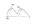
- the power supply voltage control signal generation unit 114 generates a power supply voltage control signal h according to the simple envelope g (x) input from the simple envelope generation unit 111 and the prefetch width b (n) input from the prefetch width update unit 113. (X) is created in the following procedure.
- FIG. 4 is a flowchart of processing performed by the power supply voltage control signal creation unit 114 in the first embodiment.
- FIG. 5 is a diagram illustrating an example of a power supply voltage control signal in the first embodiment.
- the power supply voltage control signal generator 114 determines whether or not (n ⁇ 1) N ⁇ x ⁇ nN (step S401), and (n ⁇ 1) ) If N ⁇ x ⁇ nN, the maximum value of the simple envelopes g (x) to g (x + b (n)) is set to h (x) (step S402). When (n ⁇ 1) N ⁇ x ⁇ nN is not satisfied, the power supply voltage control signal creation unit 114 ends this process. After step S402, the power supply voltage control signal creation unit 114 updates x (step S403).
- h (x) rises ahead of the simple envelope g (x) by the look-ahead width b (n), and the simple envelope g (x ) To g (x + b (n)), the maximum point of the maximum value h (x) is held up to the maximum point of the simple envelope g (x), and the fall is a curve along the simple envelope g (x).
- This h (x) is output from the power supply voltage control signal generator 114 to the voltage variable power supply 12 as a power supply voltage control signal.
- the voltage variable power supply 12 uses a value obtained by multiplying the value of the power supply voltage control signal h (x) input from the power supply voltage control signal creation section 114 by the amplification degree A of the amplifier section 14 as a voltage target value, and the positive power supply voltage v ( x) is output, and at the same time, the negative power supply voltage ⁇ v (x) having the same amplitude and the reverse sign as the positive power supply voltage v (x) is output.
- the power supply voltage control signal creation unit 114 creates the power supply voltage control signal h (x) corresponding to the simple envelope g (x) and the prefetch width b (n).
- FIG. 6 is a flowchart of processing performed by the prefetch width update unit 113 according to the first embodiment.
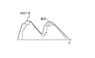
- FIG. 7 is a diagram illustrating an example of an input signal to the prefetch width update unit 113 in the first embodiment.
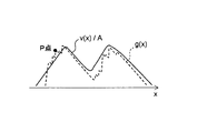
- FIG. 8 is a diagram illustrating another example of an input signal to the prefetch width update unit 113 in the first embodiment.
- the prefetch width update unit 113 attenuates the positive power supply voltage v (x) output from the voltage variable power supply 12 to 1 / A and the simple envelope g (x) created by the simple envelope creation unit 111.
- the prefetch width b (n) is updated based on the value of.
- the prefetch width b (n) is a prefetch width used in the nth frame.
- the look-ahead width updating unit 113 determines whether the positive power supply voltage v (x) is attenuated to 1 / A and the comparison result between the value of the simple envelope g (x) and The process is divided into two cases. That is, the prefetch width update unit 113 determines whether ⁇ v (x) / A ⁇ is larger than g (x) at all times x at which the simple envelope g (x) in the frame rises ( Step S601).
- step S601 the determination in step S601 is Yes.
- the output voltage of the voltage variable power supply 12 rises earlier than the audio signal amplified by the amplifier unit 14.
- the look-ahead width b (n) can be reduced to delay the rise of the output voltage of the voltage variable power supply 12.
- the prefetch width update unit 113 calculates the area S of the difference between ⁇ v (x) / A ⁇ and g (x) in the time region where the simple envelope g (x) rises (step S602).
- step S604 To reduce the prefetch width b (n) (step S604).
- step S601 in the time domain in which the simple envelope g (x) in the frame rises, for example, ⁇ v (x) / A ⁇ ⁇ g (x) as point P in FIG.
- the rise of the output voltage of the voltage variable power supply 12 is not in time for the audio signal amplified by the amplifier unit 14.
- the look-ahead width b (n) is increased to speed up the rise of the output voltage of the voltage variable power source 12.
- the prefetch width update unit 113 calculates the area R of the difference between ⁇ v (x) / A ⁇ and g (x) in the time domain where ⁇ v (x) / A ⁇ ⁇ g (x). (Step S603).
- the prefetch width b (n) is increased (step S605).
- the prefetch width update unit 113 updates the prefetch width b (n).
- the audio signal is not distorted in the amplifier unit 14, and the power efficiency of the voltage variable power source 12 can be kept high.
- the power supply voltage control signal h (x) is created while updating the prefetch width b (n), and the output voltage of the voltage variable power supply 12 follows the input audio signal by the power supply voltage control signal h (x).
- the following power supply voltage control can be performed without distorting the output signal of the amplifying apparatus 1.
- Power supply voltage control can be performed to ensure that the power supply voltage follows the audio signal. For this reason, the noise superimposed on the output signal of the amplifying apparatus 1 can be reduced as compared with the prior art.
- the amplifying apparatus 1 with improved power efficiency of the voltage variable power supply 12 can be provided.
- the present invention is an amplifying device that amplifies an input audio signal input to its own device and outputs the audio, and delays the input audio signal for a predetermined time and outputs the signal delay processing unit
- An amplifier unit that amplifies the signal output from the signal delay processing unit, a voltage variable power source that supplies power to the amplifier unit, a power source voltage control signal is output to the voltage variable power source, and the output voltage of the voltage variable power source is
- a power supply voltage control unit for controlling wherein the power supply voltage control unit calculates an envelope of the input audio signal from the input audio signal and forms a waveform formed by the power supply voltage control signal along the envelope The power supply voltage control signal is generated so that the power supply voltage control signal is generated, and the power supply voltage control signal is output to the voltage variable power supply a predetermined time before the predetermined time.
- the output voltage may be delayed from the power supply voltage control signal, but may not be accelerated. Therefore, the power supply voltage control signal is larger than the output voltage at the rising edge of the signal, and the power supply voltage control signal is smaller than the output voltage at the falling edge of the signal. Therefore, in order to keep the output voltage of the voltage variable power supply larger than the output signal of the amplifier, it is only necessary to advance the rise of the signal. Therefore, a power supply voltage control signal based on the control described above is created.
- the amplifying device reduces the headroom provided in the power supply voltage of the amplifying stage so that the output signal of the amplifying device is not distorted, and even when the capability of the voltage variable power supply fluctuates due to load fluctuations, etc. Power supply voltage control that ensures power supply voltage tracking is possible. For this reason, the noise superimposed on the output signal of the amplifying device can be reduced as compared with the prior art.
- an amplifying device with improved power efficiency of the voltage variable power supply can be provided.
- the present invention relates to an amplifying apparatus that amplifies the power of an input signal, and is particularly useful as an amplifying apparatus that performs power supply voltage control of a power supply in a signal power amplification stage.
Landscapes
- Engineering & Computer Science (AREA)
- Power Engineering (AREA)
- Physics & Mathematics (AREA)
- Nonlinear Science (AREA)
- Multimedia (AREA)
- Amplifiers (AREA)
Abstract
Description
以下、本発明の実施の形態1における増幅装置について図面を参照しながら説明する。
以下、上述した電源電圧制御信号作成部114の詳細な処理内容について説明する。以下の説明において、入力音声信号としてデジタル信号を想定し、x、N、nを整数として扱い、xを時刻として扱う。また、入力されたデジタル信号が示す値を入力順に時刻xのデータf(x)とし、さらに、連続するN点のデータ長を1フレームとして、各フレームを入力順にn番目のフレームとして処理していくこととして説明する。また、以下の説明に対応したデジタル信号の波形図である図3、図5、図7及び図8については、便宜的にデジタル信号の信号値を結んだアナログ波形として図示する。
先ず、簡易包絡線作成部111が簡易包絡線を作成する処理動作について説明する。簡易包絡線作成部111は、以下の手順で入力音声信号f(x)から簡易包絡線g(x)を得る。ここで、g(x)は、時刻xにおける簡易包絡線の信号値である。
図6は、実施の形態1における先読み幅更新部113が行う処理のフローチャートである。また、図7は、実施の形態1における先読み幅更新部113への入力信号の一例を示す図である。図8は、実施の形態1における先読み幅更新部113への入力信号の他の例を示す図である。
2 オーディオ装置
3 スピーカー
4 直流電源
11 電源電圧制御部
12 電圧可変電源
13 信号遅延処理部
14 アンプ部
15 アッテネータ部
16 A/D変換部
111 簡易包絡線作成部
112 包絡線信号遅延処理部
113 先読み幅更新部
114 電源電圧制御信号作成部
141 PWM生成部
142 ゲートドライバ
143 ハーフブリッジ回路
143a ハイサイド高速スイッチング素子
143b ローサイド高速スイッチング素子
144 ローパスフィルタ
Claims (3)
- 自装置に入力された入力音声信号を増幅して音声出力する増幅装置であって、
前記入力音声信号を所定時間遅延させて出力する信号遅延処理部と、
前記信号遅延処理部から出力された信号を増幅するアンプ部と、
前記アンプ部に電源を供給する電圧可変電源と、
前記電圧可変電源に電源電圧制御信号を出力して前記電圧可変電源の出力電圧を制御する電源電圧制御部と、を備え、
前記電源電圧制御部は、前記入力音声信号から前記入力音声信号の包絡線を算出して、前記電源電圧制御信号が成す波形を前記包絡線に沿った波形となるように前記電源電圧制御信号を作成し、前記電源電圧制御信号を前記所定時間よりも一定時間前に前記電圧可変電源へ出力する増幅装置。 - 前記電源電圧制御部は、前記アンプ部で増幅すべき音声信号に対して前記電源電圧制御信号が前もって立ち上がるように制御を行う請求項1に記載の増幅装置。
- 前記電源電圧制御部は、前記電源電圧制御信号の立下り時に、前記一定時間をゼロに設定する請求項2に記載の増幅装置。
Priority Applications (4)
| Application Number | Priority Date | Filing Date | Title |
|---|---|---|---|
| EP11731756.0A EP2432120B1 (en) | 2010-01-07 | 2011-01-05 | Amplifying device |
| US13/381,213 US8686792B2 (en) | 2010-01-07 | 2011-01-05 | Amplifying device |
| JP2011522183A JP5635507B2 (ja) | 2010-01-07 | 2011-01-05 | 増幅装置 |
| CN201180002896.1A CN102598504B (zh) | 2010-01-07 | 2011-01-05 | 放大装置 |
Applications Claiming Priority (2)
| Application Number | Priority Date | Filing Date | Title |
|---|---|---|---|
| JP2010-001695 | 2010-01-07 | ||
| JP2010001695 | 2010-01-07 |
Publications (1)
| Publication Number | Publication Date |
|---|---|
| WO2011083758A1 true WO2011083758A1 (ja) | 2011-07-14 |
Family
ID=44305494
Family Applications (1)
| Application Number | Title | Priority Date | Filing Date |
|---|---|---|---|
| PCT/JP2011/000013 WO2011083758A1 (ja) | 2010-01-07 | 2011-01-05 | 増幅装置 |
Country Status (5)
| Country | Link |
|---|---|
| US (1) | US8686792B2 (ja) |
| EP (1) | EP2432120B1 (ja) |
| JP (1) | JP5635507B2 (ja) |
| CN (1) | CN102598504B (ja) |
| WO (1) | WO2011083758A1 (ja) |
Families Citing this family (18)
| Publication number | Priority date | Publication date | Assignee | Title |
|---|---|---|---|---|
| EP2613438B1 (en) * | 2010-08-30 | 2016-04-06 | Panasonic Intellectual Property Management Co., Ltd. | Amplifier |
| KR101763410B1 (ko) * | 2010-12-21 | 2017-08-04 | 한국전자통신연구원 | 디지털 전치 왜곡 전력 증폭 장치 및 그 장치에서의 디지털 방식의 동기 조절 방법 |
| US8841894B1 (en) | 2011-12-16 | 2014-09-23 | Cirrus Logic, Inc. | Pulse-width modulated (PWM) audio power amplifier with output transition slope control |
| WO2013093989A1 (ja) * | 2011-12-19 | 2013-06-27 | 富士通株式会社 | 増幅回路 |
| WO2013186863A1 (ja) * | 2012-06-12 | 2013-12-19 | 富士通株式会社 | 増幅回路 |
| US9154095B2 (en) * | 2013-03-15 | 2015-10-06 | Bose Corporation | Boost-on-demand amplifier |
| US9184705B2 (en) | 2013-03-15 | 2015-11-10 | Bose Corporation | Feedback mechanism for boost-on-demand amplifiers |
| US9209762B1 (en) * | 2013-04-01 | 2015-12-08 | Cirrus Logic, Inc. | Switching power amplifier with rate-controlled power supply voltage transitions |
| CN103607176B (zh) * | 2013-10-21 | 2017-05-24 | 梁秀红 | 音频功放供电电路控制方法及音频功放供电电路及音频功放电路 |
| JP6252164B2 (ja) * | 2013-12-24 | 2017-12-27 | 株式会社デンソー | 車両用オーディオアンプ制御装置 |
| US9543908B2 (en) | 2014-02-21 | 2017-01-10 | Bang & Olufsen A/S | Adaptive rail voltage regulation on power supplies |
| CN105981450B (zh) * | 2014-07-30 | 2020-04-14 | 华为技术有限公司 | 功率放大器的供电电压控制方法及电子设备 |
| US10624158B2 (en) * | 2014-10-21 | 2020-04-14 | Ultraflex International Inc. | Radio frequency heating apparatus using direct-digital radio frequency power control and fine-tune power control |
| US11051369B2 (en) | 2014-10-21 | 2021-06-29 | Ultraflex International, Inc. | Radio frequency heating apparatus using direct-digital radio frequency power control and fine-tune power control |
| US9559642B2 (en) * | 2015-01-02 | 2017-01-31 | Logitech Europe, S.A. | Audio delivery system having an improved efficiency and extended operation time between recharges or battery replacements |
| KR102429755B1 (ko) * | 2015-01-28 | 2022-08-05 | 한국전자통신연구원 | 포락선-추적 전력증폭기의 포락선 신호 지연 조정 장치 및 그 방법 |
| US10250194B2 (en) * | 2015-11-13 | 2019-04-02 | Analog Devices Global | Broadband envelope tracking |
| US11750164B2 (en) * | 2020-11-17 | 2023-09-05 | Harman International Industries, Incorporated | Controlled rail-voltage decay for boost power supply output protection |
Citations (5)
| Publication number | Priority date | Publication date | Assignee | Title |
|---|---|---|---|---|
| JPH0353602A (ja) * | 1989-07-21 | 1991-03-07 | Hitachi Ltd | 増幅装置 |
| JP2007243927A (ja) * | 2006-01-27 | 2007-09-20 | Marvell World Trade Ltd | 可変パワー適応送信機 |
| WO2009019459A1 (en) * | 2007-08-03 | 2009-02-12 | Wolfson Microelectronics Plc | Amplifier circuit |
| JP2009152904A (ja) * | 2007-12-20 | 2009-07-09 | Fujitsu Ltd | 電力増幅装置 |
| JP2009177640A (ja) * | 2008-01-25 | 2009-08-06 | Fujitsu Ltd | 電力増幅器 |
Family Cites Families (14)
| Publication number | Priority date | Publication date | Assignee | Title |
|---|---|---|---|---|
| JPH05316012A (ja) * | 1992-05-07 | 1993-11-26 | Nec Corp | 出力電力制御回路 |
| DE19858963A1 (de) * | 1998-12-21 | 2000-07-13 | Becker Gmbh | Audiosignalverstärker |
| US6043707A (en) * | 1999-01-07 | 2000-03-28 | Motorola, Inc. | Method and apparatus for operating a radio-frequency power amplifier as a variable-class linear amplifier |
| GB2360410A (en) * | 2000-03-18 | 2001-09-19 | Univ Bristol | An amplifier in which the input signal is delayed to allow time for the power supply to adjust to a level which minimises power loss |
| DE10140258A1 (de) | 2001-08-16 | 2003-03-13 | Werner Ullrich | Schneckenabwehrvorrichtung |
| DE10140285A1 (de) * | 2001-08-16 | 2003-02-27 | Klein & Hummel Gmbh | Schaltungsanordnung zur Verstärkung eines Audiosignals |
| US6696866B2 (en) * | 2002-07-24 | 2004-02-24 | Motorola, Inc. | Method and apparatus for providing a supply voltage based on an envelope of a radio frequency signal |
| US6937094B2 (en) * | 2002-11-22 | 2005-08-30 | Powerwave Technologies, Inc. | Systems and methods of dynamic bias switching for radio frequency power amplifiers |
| SE0302681D0 (sv) | 2003-10-09 | 2003-10-09 | Bang & Olufsen Icepower As | Method for pulse area modulation |
| US7026868B2 (en) | 2003-11-20 | 2006-04-11 | Northrop Grumman Corporation | Variable supply amplifier system |
| US7602155B2 (en) * | 2005-07-27 | 2009-10-13 | Artesyn Technologies, Inc. | Power supply providing ultrafast modulation of output voltage |
| US7454179B1 (en) * | 2005-11-15 | 2008-11-18 | Rf Micro Devices, Inc. | Radio frequency power detector and decision circuit used with DC supply voltage controlled power amplifiers |
| US7761066B2 (en) * | 2006-01-27 | 2010-07-20 | Marvell World Trade Ltd. | Variable power adaptive transmitter |
| WO2008024666A2 (en) | 2006-08-21 | 2008-02-28 | Cirrus Logic, Inc. | Method and apparatus for controlling a selectable voltage audio power output stage |
-
2011
- 2011-01-05 JP JP2011522183A patent/JP5635507B2/ja not_active Expired - Fee Related
- 2011-01-05 EP EP11731756.0A patent/EP2432120B1/en not_active Not-in-force
- 2011-01-05 CN CN201180002896.1A patent/CN102598504B/zh active Active
- 2011-01-05 US US13/381,213 patent/US8686792B2/en active Active
- 2011-01-05 WO PCT/JP2011/000013 patent/WO2011083758A1/ja active Application Filing
Patent Citations (5)
| Publication number | Priority date | Publication date | Assignee | Title |
|---|---|---|---|---|
| JPH0353602A (ja) * | 1989-07-21 | 1991-03-07 | Hitachi Ltd | 増幅装置 |
| JP2007243927A (ja) * | 2006-01-27 | 2007-09-20 | Marvell World Trade Ltd | 可変パワー適応送信機 |
| WO2009019459A1 (en) * | 2007-08-03 | 2009-02-12 | Wolfson Microelectronics Plc | Amplifier circuit |
| JP2009152904A (ja) * | 2007-12-20 | 2009-07-09 | Fujitsu Ltd | 電力増幅装置 |
| JP2009177640A (ja) * | 2008-01-25 | 2009-08-06 | Fujitsu Ltd | 電力増幅器 |
Non-Patent Citations (1)
| Title |
|---|
| See also references of EP2432120A4 * |
Also Published As
| Publication number | Publication date |
|---|---|
| JP5635507B2 (ja) | 2014-12-03 |
| EP2432120A4 (en) | 2014-01-22 |
| US20120262232A1 (en) | 2012-10-18 |
| EP2432120B1 (en) | 2017-12-06 |
| CN102598504B (zh) | 2015-05-13 |
| EP2432120A1 (en) | 2012-03-21 |
| JPWO2011083758A1 (ja) | 2013-05-13 |
| US8686792B2 (en) | 2014-04-01 |
| CN102598504A (zh) | 2012-07-18 |
Similar Documents
| Publication | Publication Date | Title |
|---|---|---|
| JP5635507B2 (ja) | 増幅装置 | |
| JP5914842B2 (ja) | 増幅装置 | |
| JP5903638B2 (ja) | 増幅装置 | |
| US7649410B2 (en) | Systems and methods for improving performance in a digital amplifier by adding an ultrasonic signal to an input audio signal | |
| US8115564B2 (en) | Systems and methods to minimize startup transients in class-D amplifiers | |
| US11018644B2 (en) | Audio amplifier with embedded buck controller for class-G application | |
| KR100952384B1 (ko) | 파워 앰프 | |
| US7315209B2 (en) | Power amplifier apparatus and DC component removing method | |
| US7528662B2 (en) | Signal amplification apparatus and signal amplification method | |
| KR20140002180A (ko) | 리시버 회로 | |
| TW200419899A (en) | Operational amplifier with self control circuit for realizing high slew rate throughout full operating range | |
| US20210391831A1 (en) | Amplifier circuits | |
| JP7387391B2 (ja) | オーディオ回路、それを用いた電子機器および車載オーディオシステム | |
| JP2008154117A (ja) | D級アンプ | |
| KR101982065B1 (ko) | 차량용 음원 신호 증폭 장치 및 이의 방법 | |
| JP6405759B2 (ja) | 信号処理装置および信号処理方法 | |
| JP4722384B2 (ja) | 多段高出力増幅器 | |
| JP2006101022A (ja) | デジタルアンプ | |
| US20230007395A1 (en) | Audio processor | |
| WO2019235061A1 (ja) | 電源装置及び電源供給方法 | |
| US8169260B2 (en) | Amplifier circuit utilizing characteristic correction and smooth curvilinear correction | |
| JP2001196864A (ja) | 増幅回路 | |
| JP2002290160A (ja) | 高周波増幅器 | |
| JP2013187770A (ja) | 増幅装置 |
Legal Events
| Date | Code | Title | Description |
|---|---|---|---|
| WWE | Wipo information: entry into national phase |
Ref document number: 201180002896.1 Country of ref document: CN |
|
| WWE | Wipo information: entry into national phase |
Ref document number: 2011522183 Country of ref document: JP |
|
| 121 | Ep: the epo has been informed by wipo that ep was designated in this application |
Ref document number: 11731756 Country of ref document: EP Kind code of ref document: A1 |
|
| WWE | Wipo information: entry into national phase |
Ref document number: 2011731756 Country of ref document: EP |
|
| WWE | Wipo information: entry into national phase |
Ref document number: 13381213 Country of ref document: US |
|
| NENP | Non-entry into the national phase |
Ref country code: DE |