WO2011065282A1 - ツイストボール型電子ペーパー - Google Patents
ツイストボール型電子ペーパー Download PDFInfo
- Publication number
- WO2011065282A1 WO2011065282A1 PCT/JP2010/070588 JP2010070588W WO2011065282A1 WO 2011065282 A1 WO2011065282 A1 WO 2011065282A1 JP 2010070588 W JP2010070588 W JP 2010070588W WO 2011065282 A1 WO2011065282 A1 WO 2011065282A1
- Authority
- WO
- WIPO (PCT)
- Prior art keywords
- base material
- twist ball
- counter electrode
- electronic paper
- substrate
- Prior art date
- Legal status (The legal status is an assumption and is not a legal conclusion. Google has not performed a legal analysis and makes no representation as to the accuracy of the status listed.)
- Ceased
Links
Images




Classifications
-
- G—PHYSICS
- G09—EDUCATION; CRYPTOGRAPHY; DISPLAY; ADVERTISING; SEALS
- G09F—DISPLAYING; ADVERTISING; SIGNS; LABELS OR NAME-PLATES; SEALS
- G09F9/00—Indicating arrangements for variable information in which the information is built-up on a support by selection or combination of individual elements
- G09F9/30—Indicating arrangements for variable information in which the information is built-up on a support by selection or combination of individual elements in which the desired character or characters are formed by combining individual elements
- G09F9/37—Indicating arrangements for variable information in which the information is built-up on a support by selection or combination of individual elements in which the desired character or characters are formed by combining individual elements being movable elements
- G09F9/372—Indicating arrangements for variable information in which the information is built-up on a support by selection or combination of individual elements in which the desired character or characters are formed by combining individual elements being movable elements the positions of the elements being controlled by the application of an electric field
-
- G—PHYSICS
- G02—OPTICS
- G02B—OPTICAL ELEMENTS, SYSTEMS OR APPARATUS
- G02B26/00—Optical devices or arrangements for the control of light using movable or deformable optical elements
- G02B26/02—Optical devices or arrangements for the control of light using movable or deformable optical elements for controlling the intensity of light
- G02B26/026—Optical devices or arrangements for the control of light using movable or deformable optical elements for controlling the intensity of light based on the rotation of particles under the influence of an external field, e.g. gyricons, twisting ball displays
Definitions
- the present invention relates to a twist ball type electronic paper using a twist ball as a display medium.
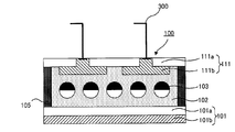
- FIG. 8 is a schematic cross-sectional view showing an example of such electronic paper.
- the electronic paper 100 includes a common electrode side base material 101 having a first base material 101a and a common electrode 101b formed on the first base material 101a, and a common electrode of the common electrode side base material 101.
- the first base material 101a opposite to the 101b side is disposed on the twist ball 103 and the twist ball layer 102 containing a low-polar solvent, and the second base material 111a and the second base material 111a are disposed on the twist ball layer 102.
- a display electrode side substrate 111 having a display electrode 111b formed in a pattern on the substrate is provided. Further, the display electrode side substrate 111 is disposed so that the display electrode 111 b faces the twist ball layer 102 side, and the end of the electronic paper 100 is sealed with a sealant 105.
- the display electrode 111b and the twist ball layer 102 are in direct contact with each other, the display electrode material may be eluted into the low polarity solvent of the twist ball layer 102, which may deteriorate the image display of the electronic paper. was there.
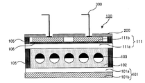
- the electronic paper 100 shown in FIG. 9 has a configuration in which a display electrode 111b is formed on a fixed substrate 200, and this is disposed on a second base material 111a via a sealant 105, an adhesive 106, and the like. Further, the electronic paper 100 shown in FIG. 10 has a twisted ball layer 102 composed of a low polarity solvent and a twist ball 103 sealed with a film-like first base material 101a and a film-like second base material 111a, and a fixed substrate. The display electrode 111 b formed on the substrate 200 is arranged with an adhesive 106 interposed therebetween. Note that reference numerals not described in FIG. 9 and FIG.
- the twisting ball layer 102 composed of the low polarity solvent and the twisting ball 103 is completely sealed by the first base material 101a and the second base material 111a, so that the display electrode as shown in FIG. There is no need for a process of completely closing the through hole used for connecting the wiring 111b to the wiring 111b.
- the twist ball layer 102 and the display electrode 111b are not in direct contact with each other, so that it is possible to prevent the display electrode material from being eluted into the low polarity solvent of the twist ball layer 102.
- the second base material 111a is a flexible film base material
- the display electrode 111b formed on the fixed substrate 200 and the second base material 111a are arranged via the adhesive 106, the display electrode
- the yield of bonding between the fixed substrate 200 and the second base material 111a due to the unevenness of the 111b may be reduced and the image display of the electronic paper may be deteriorated.
- the transparent electrode side having the counter electrode formed in a stripe shape on the fixed substrate, the first base material, and the transparent electrode formed on the first base material The base material, the transparent electrode side base material is disposed on the first base material opposite to the transparent electrode side, the twist ball layer including a twist ball and a low polarity solvent, and the twist ball layer disposed on the twist ball layer
- a configuration in which the counter electrode and the second base material are arranged via an adhesive or the like has been proposed.
- problems such as a decrease in the yield of bonding between the substrate and the second base material, and a possibility that the image display of the electronic paper is deteriorated.
- the present invention provides a first substrate made of a transparent film, a transparent electrode side substrate having a transparent electrode formed on one surface of the first substrate, and insulation.
- a second substrate made of a film having a property, a counter electrode side substrate having a counter electrode formed on one surface of the second substrate, and a low polarity solvent layer containing a twist ball and a low polarity solvent
- a twist ball layer wherein the twist ball layer is sealed by the first base material and the second base material, and the counter electrode side base material is configured such that the counter electrode is opposite to the twist ball layer.
- a twisting ball type electronic paper which is arranged as described above.
- the counter electrode since the counter electrode is not in direct contact with the twist ball layer, it is possible to prevent image display deterioration due to elution of the material of the counter electrode into the low polarity solvent. In addition, it is possible to prevent a decrease in yield at the time of bonding due to the unevenness of the counter electrode and deterioration of image display of the twisting ball type electronic paper. Furthermore, when the twist ball type electronic paper of the present invention is an electronic paper used for a segment application (hereinafter sometimes referred to as an electronic paper for a segment), the counter electrode side substrate is the counter electrode is the above. The wiring can be easily taken out by being disposed on the side opposite to the twist ball layer.
- the first base material and the second base material are made of materials that can be laminated, and the twist ball layer is sealed by laminating the first base material and the second base material. It is preferable that Since the twist ball layer is sealed by laminating the first base material and the second base material, the display area of the twist ball type electronic paper of the present invention is compared with, for example, a case where a sealant or the like is used. Can be made in a wide range.
- the sealing method is a twisting ball layer sealing method in which no sealant is arranged on the outer periphery of the twisting ball layer, when tiling a plurality of display panels side by side, the effect on the display due to the joint between the panels can be reduced. Is possible. This is because the heat-sealed portion of the both substrates of the film by laminating can be arranged on the side surface or the back surface of the display surface using the plasticity of the film.
- the present invention also provides a first base material comprising a transparent film, a transparent electrode side base material having a transparent electrode formed on one surface of the first base material, and a film-like holding base material having insulation properties.
- a twisting ball member comprising a twisting ball layer comprising a twisting ball and a low polarity solvent layer containing a low polarity solvent, wherein the twisting ball layer is sealed with the first base material and the holding base material, and insulated
- a counter electrode side base material having a counter electrode formed on one surface of the second base material, wherein the counter electrode side base material is the twist
- a twisted ball type electronic paper characterized in that the counter electrode is disposed on the outer side of a holding base of a ball member so as to be opposite to the twisted ball member.
- the counter electrode since the counter electrode is not in direct contact with the twist ball layer, it is possible to suppress deterioration in image display due to the counter electrode material being eluted in the low polarity solvent. In addition, it is possible to prevent a decrease in yield at the time of pasting due to the unevenness of the counter electrode and deterioration of image display of electronic paper.
- the twist ball type electronic paper of the present invention is an electronic paper for a segment
- the counter electrode side base material is disposed outside the twist base material holding base, and the counter electrode is connected to the twist ball member. By arranging them so as to be on the opposite side, the wiring can be easily taken out.
- the counter electrode side base material since the counter electrode side base material is disposed outside the holding base material of the twist ball member, only the counter electrode side base material disposed on the twist ball member is replaced. Thus, the twist ball type electronic paper can be easily reused.
- the counter electrode side substrate is disposed on the surface of the holding substrate opposite to the twist ball member via a removable adhesive. This is because the counter electrode side substrate can be easily replaced by using a re-peelable adhesive.
- the first base material and the holding base material are made of a material that can be laminated, and the twist ball layer is sealed by laminating the first base material and the holding base material.
- the twist ball layer is sealed by laminating the first base material and the holding base material, for example, the twist ball layer is sealed using a sealant or the like.
- the display area of the twisting ball type electronic paper of the invention can be widened.
- the sealing method is a twisting ball layer sealing method in which no sealant is arranged on the outer periphery of the twisting ball layer, when tiling a plurality of display panels side by side, the effect on the display due to the joint between the panels can be reduced. Is possible. This is because the heat-sealed portion of the both substrates of the film by laminating can be arranged on the side surface or the back surface of the display surface using the plasticity of the film.
- the twist ball type electronic paper of the present invention has the configuration as described above, the twist ball layer and the counter electrode are not in direct contact with each other, so that the counter electrode material is eluted in the low polarity solvent of the twist ball layer. It is possible to prevent image display deterioration. In addition, it is possible to prevent a decrease in yield at the time of pasting due to the unevenness of the counter electrode and deterioration of image display of electronic paper.
- the twist ball type electronic paper of the present invention is an electronic paper for a segment, the counter electrode side base material is disposed so that the counter electrode is opposite to the twist ball layer. Therefore, the wiring of the counter electrode can be easily taken out.
- the twist ball type electronic paper of the present invention has a configuration in which the counter electrode side base material is disposed outside the holding base material of the twist ball member, and therefore only replaces the counter electrode side base material. Therefore, it becomes possible to reuse easily.
- the twist ball type electronic paper of the present invention (hereinafter sometimes simply referred to as electronic paper) will be described.
- the electronic paper of the present invention is roughly classified into two modes depending on the position of the counter electrode.
- the electronic paper of each aspect will be described.
- the electronic paper of the present aspect includes a first base material made of a transparent film, and a transparent electrode side base material having a transparent electrode formed on one surface of the first base material, A second base material made of an insulating film, a counter electrode side base material having a counter electrode formed on one surface of the second base material, and a low polarity solvent layer containing a twist ball and a low polarity solvent A twist ball layer, wherein the twist ball layer is sealed by the first base material and the second base material, and the counter electrode side base material is configured such that the counter electrode is opposite to the twist ball layer. It arrange
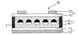
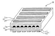
- FIG. 1A is a schematic view showing an example of the electronic paper of this embodiment
- FIG. 1B is a schematic cross-sectional view taken along the line AA in FIG.
- the electronic paper of this aspect is the electronic paper for segments
- the electronic paper 10 of this aspect is transparent which has the 1st base material 11 which consists of a film which has transparency, and the transparent electrode 12 formed in one surface of a 1st base material.
- Electrode side base material 1 second base material 21 made of an insulating film, counter electrode side base material 2 having counter electrode 22 formed on one surface of second base material 21, and twist ball 3a And a twist ball layer 3 composed of a low polarity solvent layer 3b containing a low polarity solvent.
- the twist ball layer 3 is sealed by a first base material 11 and a second base material 21, and the counter electrode side base material 2 is The counter electrode 22 is disposed on the side opposite to the twisting ball layer 3.
- the counter electrode 22 and the counter electrode side base material 2 are used as a display electrode and a display electrode side base material.
- the transparent electrode 12 and the transparent electrode side base material 1 are used as a common electrode and a common electrode side base material.
- 1 shows an example in which the twisted ball layer 3 is hermetically sealed by laminating the first base material 11 and the second base material 21, but as shown in FIG.
- the twist ball layer 3 may be sealed by disposing the sealing agent 4 between the first base material 11 and the second base material 21. 2 that are not described in FIG. 2 can be the same as those in FIG.
- FIG. 3 is a schematic diagram illustrating another example of the electronic paper of this aspect.
- FIG. 3 shows a case where the electronic paper of this embodiment is a passive drive type electronic paper.
- the transparent electrode 12 and the counter electrode 22 are formed on each base material in stripes so as to cross each other.
- the electronic paper 10 is a passive drive type electronic paper
- one of the transparent electrode 12 and the counter electrode 22 formed in the stripe shape is a scanning (row) electrode
- the other is used as a signal (column) electrode. 3 that are not described in FIG. 3 can be the same as those in FIG.
- FIG. 4 is a schematic cross-sectional view illustrating an example of electronic paper.
- a permanent dipole is formed by charging a black phase portion with a positive charge and charging a white phase portion with a negative charge.
- the said 1st base material 11 shall have insulation.
- the twist ball 3a sandwiched between the transparent electrode 12 and the counter electrode 22 is placed under the electric field.
- the black phase is charged with a positive charge and the white phase is charged with a negative charge.
- each twist ball 3a (FIG. 4A )),
- the black phase of the twist ball 3a faces the second substrate 21 side, and the white phase of the twist ball 3a faces the first substrate 11 side (FIG. 4B).
- the black phase of the twist ball faces the first substrate side, and the white phase of the twist ball is the second group. It comes to face the material side.
- image display can be performed by controlling the direction of the twist ball.
- FIG. 4 it is shown in a simplified manner that the twist ball layer 3 is sealed by laminating the first base material 11 and the second base material 21.
- reference numerals not described in FIG. 4 can be the same as those in FIG.
- the twist ball has a charge
- the electronic paper is configured such that the twist ball layer 102 and the display electrode 111b are in direct contact
- the twist ball layer There is a problem that the display electrode material having conductivity eluted in the low-polarity solvent 102 may affect the twist ball 103, and the display quality of the electronic paper may be deteriorated.
- the wiring 300 is taken out from the display electrode 111b, it is necessary to take out the wiring 300 by providing a through hole in the second base material 111a in accordance with the formation position of the display electrode 111b, and the pattern of the display electrode 111b is fine.
- FIG. 8 shows an example of segmented electronic paper, although not shown, even in passive drive type electronic paper, when the counter electrode and the twist ball layer are in direct contact with each other, There has been a problem that the display quality of the paper may deteriorate.
- the counter electrode since the counter electrode does not directly contact the twist ball layer, the counter electrode material does not elute in the low polarity solvent contained in the twist ball layer. Deterioration can be suppressed.
- the display electrode 111b is formed on the fixed substrate 200, and this is disposed on the second base material 111a.
- the display electrode 111b is formed on the fixed substrate 200, and this is disposed on the second base material 111a.
- the second base material 111a is a film base material having plasticity
- the display electrode 111b formed on the fixed substrate 200 and the second base material 111a are disposed via the adhesive 106, the display electrode 111b
- the yield of bonding between the fixed substrate 200 and the second base material 111a due to the unevenness may be reduced and the image display of the electronic paper may be deteriorated.
- FIG. 9 and FIG. 10 show an example of the segmented electronic paper, although not shown, even in the passive drive type electronic paper, the decrease in yield during the production of the electronic paper due to the unevenness of the counter electrode, The deterioration of electronic paper image display is a problem.
- the counter electrode is arranged on the side opposite to the twist ball layer, the yield at the time of bonding due to the unevenness of the counter electrode and the deterioration of the image display of the electronic paper are reduced. Can be prevented. Furthermore, when the electronic paper of this aspect is an electronic paper for segments, the wiring of the counter electrode can be easily taken out by arranging the counter electrode on the side opposite to the twist ball layer. It is. Hereinafter, each structure of the electronic paper of this aspect is demonstrated.
- the counter electrode side base material used for this aspect has the 2nd base material which consists of a film which has insulation, and the counter electrode formed in one surface of the said 2nd base material. Is. Such a counter electrode side base material is disposed and used such that the counter electrode is on the side opposite to a twist ball layer described later.
- the said counter electrode side base material shall be used as a display electrode side base material.
- the counter electrode is used as a display electrode.
- the electronic paper of this aspect is a passive drive type electronic paper, one of the counter electrode and the transparent electrode described later is used as a scanning (row) electrode, and the other is used as a signal (column) electrode. .
- the counter electrode is not particularly limited as long as it is made of a conductive material and can display an image using a twist ball layer described later by applying a voltage to the counter electrode.
- the counter electrode may be directly formed on the second base material, and for example, an adhesive layer or the like is interposed between the second base material and the counter electrode.
- the counter electrode is formed on a film different from the second base material, and the film on which the counter electrode is formed is disposed on the second base material. May be. In this embodiment, for simplification of the process, it is more preferable that the counter electrode is directly formed on the second base material.
- the shape of the counter electrode used in this embodiment is particularly limited if the electronic paper of this embodiment is an electronic paper for segments, as long as it has a shape that matches the displayed pattern. is not. Specific examples include characters and designs.
- the counter electrode when the electronic paper of this embodiment is a passive drive type electronic paper, the counter electrode usually has a pattern corresponding to a pattern of a transparent electrode described later, as shown in FIG. Such a pattern of the counter electrode can be the same as the pattern of the counter electrode used in a general passive drive display device, and thus description thereof is omitted here.
- the material used for such a counter electrode is not particularly limited as long as it is a conductive material.
- metals such as Au, Al, Ag, Ni, and Cu, ITO, SnO 2 , and ZnO: Examples thereof include a transparent conductor such as Al, a mixture of a conductive agent in a solvent or a synthetic resin binder, and the like.
- the conductive agent include cationic polymer electrolytes such as polymethylbenzyltrimethyl chloride and polyallylpolymethylammonium chloride, anionic polymer electrolytes such as polystyrene sulfonate and polyacrylate, electron conductive zinc oxide, and oxidation. Tin, indium oxide, carbon fine powder, Ag fine powder or the like is used.
- the material used for the counter electrode is, among other things, a conductive material that is flexible and can withstand expansion and contraction of the substrate in consideration of conductivity and formation on the film substrate.
- a conductive paste in which a metal such as Cu, Al, or Ag, carbon, Ag fine powder, or the like is mixed with a synthetic resin binder is preferable.
- the above-described metal, the transparent conductor, and the like are sputtered using a metal mask or the like, or a vacuum deposition method.
- a method of forming a thin film in a pattern on the second substrate by a CVD method, a coating method, etc., a method of applying the conductive agent in a solvent or a synthetic resin binder and applying the pattern on the second substrate, etc. can be mentioned.
- the counter electrode when the counter electrode is formed on the second base material, which will be described later, via an adhesive or the like, the metal foil made of the metal is cut into a predetermined shape, and this is pasted on the second base material with the adhesive or the like.
- the method of attaching is mentioned.
- positioning the said counter electrode on the said 2nd base material through a film different from a 2nd base material a counter electrode is formed in the said film in pattern shape, and this is formed through an adhesive agent etc. Examples include a method of disposing on the second substrate, a method in which the above-described metal, transparent conductor, and the like deposited on the entire surface are cut into a predetermined shape, and this is attached to the second substrate with an adhesive or the like. .
- the said counter electrode As a film in which the said counter electrode is formed, it shall consist of the material similar to a 2nd base material. Moreover, about the said adhesive agent etc., since it can be the same as that used when sticking an electrode on a resin base material in a general electrode member, description here is abbreviate
- the film thickness of the counter electrode can be formed with a uniform film thickness on the surface opposite to the twist ball layer side of the second base material described later, and image display can be performed with the electronic paper of this embodiment.
- it is not particularly limited as long as it has a film thickness of about a degree, specifically, it is in the range of 50 nm to 500 ⁇ m, especially in the range of 100 nm to 100 ⁇ m, particularly in the range of 300 nm to 50 ⁇ m.
- the thickness of the counter electrode is less than the above range, it is difficult to form a counter electrode having a uniform thickness. If the thickness exceeds the above range, it takes time to form the counter electrode. In addition, since a large amount of material for the counter electrode is required, the manufacturing cost increases.
- the 2nd base material used for this aspect consists of a film which has insulation, and the said counter electrode is formed on one surface of a 2nd base material. Moreover, the twist ball layer mentioned later is sealed with the 1st base material used for the transparent electrode side base material mentioned later.
- the 2nd base material used for this aspect will not be specifically limited if it has a self-supporting property of the grade which can form a counter electrode on the said 2nd base material. Moreover, as said 2nd base material, although it may have transparency and does not need to have transparency, what does not have transparency is more preferable.
- image display is observed from the transparent electrode side. Therefore, in this embodiment, when the electronic paper is observed from the transparent electrode side, the second base material is disposed on the lower layer side of the twist ball layer that performs image display. This is because problems such as light leakage are considered to occur.
- the material for the second substrate is not particularly limited as long as it is a general plastic material, but polypropylene, polyethylene, polyvinyl chloride, polystyrene, polyvinyl alcohol, polyimide, polyethylene naphthalate, polyethylene terephthalate, polycarbonate, Examples include polyetherimide, polyetheretherketone, polyetherketone, polyphenylene sulfide, liquid crystal polymer, epoxy resin, silicone resin, and phenol resin.
- the twist ball layer described later it is preferable to seal the twist ball layer described later by laminating a first substrate and a second substrate described later.
- laminating it is more preferable to use a base material on which a base film material capable of laminating and a sealant film material described later are laminated as the second base material.
- the base film material that can be laminated is polyimide, polyethylene naphthalate, polyethylene terephthalate, polycarbonate, polyetherimide, poly, from the viewpoint of heat resistance by thermocompression bonding during lamination.
- Examples include ether ether ketone, polyether ketone, polyphenylene sulfide, liquid crystal polymer, epoxy resin, silicone resin, and phenol resin.
- a sealant film material a non-stretched polypropylene film, a biaxially stretched polypropylene film, etc. are mentioned. It is also possible to use a coating film made of a heat-sealable material such as polyurethane, polyacryl, epoxy resin, or silicone.
- a heat-sealable material such as polyurethane, polyacryl, epoxy resin, or silicone.
- the materials are the same base film material and sealant film material.
- the second base material and the first base material described later are the same base film material and sealant film material, thereby improving the adhesion between the second base material and the first base material when laminating. Because it becomes possible.
- the film thickness of the second substrate is not particularly limited as long as the counter electrode can be formed.
- the film thickness is in the range of 10 ⁇ m to 300 ⁇ m, and in particular, 15 ⁇ m to It is preferably in the range of 100 ⁇ m, particularly in the range of 25 ⁇ m to 50 ⁇ m. If the film thickness of the second base material is less than the above range, it is difficult to form the counter electrode on the second base material, and the film thickness of the second base material is within the above range. This is because, when the display is performed using the electronic paper of this aspect, the second base material is thick, and thus it may not be possible to perform image display using a twist ball. Moreover, since the 2nd base material is thick, the flexibility of the electronic paper of this aspect may fall.
- the transparent electrode side base material used for this aspect has the 1st base material which consists of a film which has transparency, and the transparent electrode formed in one surface of the said 1st base material. Is.
- a transparent electrode side base material shall be used as a common electrode side base material.
- the 1st base material used for this aspect consists of a film which has transparency, and the transparent electrode mentioned later is formed in one surface of a 1st base material. Moreover, the twist ball layer described later is sealed together with the second substrate used for the counter electrode side substrate described above.
- a 1st base material used for this aspect is a film which has transparency, and if it can form the transparent electrode mentioned later on the surface of the 1st base material, it will not be limited in particular, It may have insulating properties or may not have insulating properties, but those having insulating properties are preferable. Since the first base material has insulating properties, in the electronic paper of this aspect, it is possible to suitably perform image display using the twist ball in the twist ball layer.
- the material of the first base material is not particularly limited as long as it is a plastic material having transparency. Specifically, the same material as the material of the second base material described above is used. The description here is omitted.
- a material that can be laminated is used as the material of the first base material. More preferred. Since the material that can be laminated can be the same as the material that can be laminated used for the second base material, the description thereof is omitted here.
- the film thickness of the first base material is not particularly limited as long as it has a self-supporting property capable of forming a transparent electrode described later.
- the film thickness of the first substrate is preferably in the range of 10 ⁇ m to 300 ⁇ m, more preferably in the range of 15 ⁇ m to 100 ⁇ m, and particularly preferably in the range of 25 ⁇ m to 50 ⁇ m.
- the film thickness of the first base material is less than the above range, it is difficult to form a transparent electrode, which will be described later, on the surface of the first base material. If the range is exceeded, the first base material is thick, so that image display cannot be performed, and the flexibility of the electronic paper of this aspect may be reduced.
- the transparent electrode used for this aspect is formed on the said 1st base material.
- the said transparent electrode shall be used as a common electrode.
- the electronic paper of this aspect is passive drive type electronic paper, one of the above-described counter electrode and transparent electrode is used as a scanning (row) electrode and the other is used as a signal (column) electrode.
- Such a transparent electrode is not particularly limited as long as it is formed on the first base material.
- the transparent electrode may be directly formed on the first base material. You may form by forming a transparent electrode on the film which has transparency, and arrange
- Examples of such a transparent electrode material include ITO, SnO 2 , ZnO: Al, and other transparent conductors.
- the said transparent electrode is normally formed in the 1st base material whole surface mentioned above, when the said transparent electrode is a common electrode.
- the transparent electrode is an electrode used for passively driven electronic paper, the transparent electrode is formed to have a pattern corresponding to the pattern of the counter electrode.
- Such a pattern of the transparent electrode can be the same as the pattern of the transparent electrode used in a general passive drive type display device, and thus description thereof is omitted here.
- the formation method of the said transparent electrode will not be specifically limited if a transparent electrode can be formed on a 1st base material with the desired film thickness.
- a transparent electrode when the transparent electrode is directly formed on the first substrate, the above-described transparent conductor is used to form a sputtering method, a vacuum deposition method, a CVD method, a coating method, or the like.
- the method of forming a thin film on the said 1st base material can be mentioned.
- the transparent electrode is formed on a transparent film and the transparent film on which the transparent electrode is formed is disposed on the first substrate, the transparent electrode is formed on the first substrate.
- a method of forming a transparent electrode on a transparent film in the same manner as in the case of directly forming the film on the first substrate using an adhesive or the like, and the transparent electrode was formed.
- Examples thereof include a film having transparency and a method of laminating the first substrate.
- a film which has the said transparency what consists of a material similar to the 1st base material mentioned above specifically can be used.
- the adhesive having transparency and the like can be the same as that used when pasting general resin substrates together, description thereof is omitted here.
- the film thickness of the transparent electrode used in this embodiment is not particularly limited as long as it can be formed on the surface of the first base material.
- the film thickness of such a transparent electrode is preferably in the range of 50 nm to 10 ⁇ m, more preferably in the range of 100 nm to 5 ⁇ m, and particularly preferably in the range of 200 nm to 1 ⁇ m. This is because, when the film thickness of the transparent electrode is less than the above range, it is difficult to form the transparent electrode with a uniform film thickness on the surface of the first base material. In addition, when the film thickness of the transparent electrode exceeds the above range, the manufacturing cost increases because the time and material used for forming the transparent electrode increase.
- (C) Transparent electrode side base material The arrangement of the transparent electrode side base material used in the present embodiment is not particularly limited as long as desired display can be performed using the electronic paper of the present embodiment.
- the transparent electrode side base material may be disposed so that the transparent electrode is on the twist ball layer side described later, and for example, the transparent electrode is opposite to the twist ball layer. You may arrange
- the transparent electrode side base material is disposed so that the transparent electrode is on the side opposite to the twist ball layer.
- the transparent electrode does not come into direct contact with the twisting ball layer, so the transparent electrode material does not elute in the low polarity solvent of the twisting ball layer. Can be prevented. Further, when a material that does not easily dissolve in a low-polar solvent is used as the material for the transparent electrode, the transparent electrode side substrate may be disposed so that the transparent electrode is on the twist ball layer side described later. .
- the electronic paper of this aspect is a passive drive type electronic paper
- the transparent electrode is formed in a pattern such as a stripe shape, when the transparent electrode is arranged on the side opposite to the twist ball layer, the unevenness of the transparent electrode This is because image display deterioration of the electronic paper can be prevented, and furthermore, wiring can be easily connected without installing a through hole in the transparent electrode side base material.
- twist ball layer used in this embodiment is composed of a low polarity solvent layer containing a twist ball and a low polarity solvent, and the first substrate and the counter electrode used for the transparent electrode side substrate. It is sealed by the second base material used for the side base material.
- the sealing method is not particularly limited.
- the twist base layer is not limited.
- a method of sealing the twisted ball layer by disposing a sealing agent for sealing between the second substrate and the first substrate of the transparent electrode side substrate, for example.
- a method of sealing the twist ball layer by laminating the first base material and the second base material using a material that can be laminated on the second base material of the counter electrode side base material. .
- a method of sealing the twisted ball layer by laminating is more preferable.
- the method of sealing the twist ball layer by the laminating process can make the display area of the electronic paper wider than the method using a sealing agent, and when tiling a plurality of display panels side by side. It is possible to reduce the influence on the display by the joint between the panels. This is because the heat-sealed portions of the both substrates of the film by lamination can be arranged on the side surface or the back surface of the display surface by utilizing the plasticity of the film.
- the twist ball layer when the twist ball layer is sealed with a sealant, the transparent electrode side base material and the counter electrode side base material have flexibility. There is a problem that liquid leakage of a low polarity solvent in the ball layer may occur. On the other hand, when the twist ball layer is sealed by laminating, the twist ball layer laminated by the first base material and the second base material becomes easy to handle.
- the method of sealing the twist ball layer by laminating can be the same as that of general laminating, and therefore description thereof is omitted here. Further, the sealing method using the sealant can be the same as the sealing method by bonding together common base materials, and thus description thereof is omitted here.
- the twist ball layer used in this embodiment is composed of a low polarity solvent layer including a twist ball and a low polarity solvent, and can be sealed with the first base material and the second base material described above.
- the paper is not particularly limited as long as a desired image display can be performed.
- the twist ball used for such a twist ball layer and the low polarity solvent layer will be described respectively.
- twist ball used in this embodiment is included in the twist ball layer and serves as a display medium in the electronic paper of this embodiment.
- the twist ball used in this embodiment is spherical and has two hues of colored hue / white hue or colored hue / colored layer, and two different hues having different dipoles. It is not particularly limited.
- twist ball can be the same as the twist ball manufactured by the microchannel manufacturing method proposed in Japanese Patent Application Laid-Open No. 2004-197083.
- the colored continuous phase and the spherical particleized phase are in an O / W type or W / O type relationship with each other, and from the first microchannel in which the colored continuous phase is transferred, Bipolar spherical polymer particles that are discharged in a spherical particle phase of a flowing medium flowing through the second microchannel in sequence, and having a positive ( ⁇ ) polarity.
- the polymerizability in a colored continuous phase in which an oily or aqueous fluid medium containing a polymerizable resin component is phase-separated into two colors containing a coloring dye or pigment insoluble in this medium.
- the resin component is formed with different positively and negatively charged polymerizable monomers, transferred to the first microchannel, and this colored continuous phase is then transferred into the aqueous or oily spherical particleized phase flowing in the second microchannel.
- the liquid is sequentially or intermittently discharged.
- the discharged material discharged into the spherical particle phase is gradually formed into spherical particles during the series of discharge, dispersion, and transfer in the microchannel, and then into spherical particles.
- a twist ball is appropriately prepared by polymerizing and curing the polymerizable resin component in the activated particles under UV irradiation and / or heating.
- the colored continuous phase is a continuous hue divided into two hues, for example, any one of black / white, red / white, yellow / white, blue / white, green / white, purple / white, etc.
- Examples thereof include any two-color hue separation hues selected from “chromatic hue / white hue” or two-color hue separation hues having different color hue / color layers.
- the colorant for forming such a hue is appropriately selected and used without particular limitation as long as it is insoluble or uniformly dispersed in a fluid dispersion medium containing a polymerizable resin component described later.
- the colorant dyes and pigments can be used.
- the addition amount of the dyes and pigments as these colorants is not particularly limited, and the desired color tone varies depending on the use of the colored particles, and the dispersibility in the above-described colored continuous phase, etc. Therefore, in this embodiment, the amount is 0.1 to 80 parts by weight, preferably 2 to 10 parts by weight, per 100 parts by weight of the total polymerizable resin component which is a polymerization and curing component in the colored continuous phase. It can add suitably suitably.
- the chargeability of the twist ball depends on the kind of the functional group or substituent of the polymerizable monomer used in the twist ball. And monomer species that tend to exhibit (+) chargeability. Therefore, in the case where at least two or more types of monomers are used as the polymerizable resin component in this embodiment, the tendency to show the (+) and ( ⁇ ) chargeability is well known, A plurality of monomers having a tendency to property can be used in combination as appropriate.
- examples of the functional group or substituent include a carbonyl group, a vinyl group, a phenyl group, Examples thereof include an amino group, an amide group, an imide group, a hydroxyl group, a halogen group, a sulfonic acid group, an epoxy group, and a urethane bond.
- it can use suitably suitably combining the monomer type which has a functional group or a substituent in such a polymerizable monomer individually or in combination of 2 or more types.
- ( ⁇ ) chargeable monomer and the (+) chargeable polymerizable monomer those described in Japanese Patent Application Laid-Open No. 2004-197083 can be used. Description is omitted.
- the monomer having a tendency to be charged on a weight basis is preferably in the range of 1% to 100% of the total monomers, More preferably, it is suitably used as long as it is a copolymer particle with a polymerizable monomer in the range of 5% to 100%, particularly preferably in the range of 10% to 100%, to provide a desired twist ball. it can.
- the twist ball is a spherical monodisperse particle having an average particle diameter in the range of 1.0 ⁇ m to 400 ⁇ m, preferably in the range of 20 ⁇ m to 200 ⁇ m, more preferably in the range of 50 ⁇ m to 50 ⁇ m. It can be suitably prepared within the range of 120 ⁇ m. In addition, uniform particles with extremely low variation in average particle diameter are appropriately prepared. In this embodiment, the degree of uniformity is expressed as a Cv value and is suitably used as a twist ball of monodisperse particles of 20% or less, preferably 5% or less, more preferably 3% or less.
- the low polarity solvent layer used in this embodiment is not particularly limited as long as it contains a low polarity solvent.
- the low-polarity solvent layer is usually composed of a low-polarity solvent and an elastomer sheet made of an elastomer material that swells the low-polarity solvent.
- the low polarity solvent used in the low polarity solvent layer and the elastomer sheet will be described.
- (I) Low-polar solvent The low-polar solvent used in this embodiment is used for smooth rotation of the twist ball described above. Moreover, it is normally used by swelling in an elastomer sheet described later.
- Such a low-polar solvent is not particularly limited as long as it can be smoothly rotated without hindering the rotation of the twist ball.
- Examples of such a low polarity solvent include dimethyl silicone oil, isoparaffinic solvents, and linear alkanes such as linear paraffinic solvents, dodecane, and tridecane.
- Elastomer sheet used in this embodiment is made of an elastomer material capable of swelling the low-polarity solvent.
- the elastomer sheet is a sheet-like member in which the twist balls are dispersed, and is used by swelling the low-polarity solvent therein.
- the material used for such an elastomer sheet is not particularly limited as long as the twist ball can be dispersed and the low polarity solvent can be swollen.
- Examples of the material for such an elastomer sheet include silicone resin, (microcrosslinked) acrylic resin, (microcrosslinked) styrene resin, and polyolefin resin.
- the film thickness of the elastomer sheet is not particularly limited as long as the electronic paper of this embodiment can display an image with a twist ball dispersed in the elastomer sheet, but the film thickness is 50 ⁇ m to 1000 ⁇ m. Within the range, it is particularly preferable to be within the range of 100 ⁇ m to 700 ⁇ m, particularly within the range of 200 ⁇ m to 500 ⁇ m. When the film thickness of the elastomer sheet is less than the above range, it is difficult to obtain an elastomer sheet in which the twist balls are uniformly dispersed. When the film thickness of the elastomer sheet exceeds the above range, This is because the twist ball may be prevented from rotating.
- the film thickness of the twist ball layer used in this embodiment is not particularly limited as long as image display can be performed by rotating the twist ball in the electronic paper of this embodiment. However, it is preferably in the range of 50 ⁇ m to 1000 ⁇ m, more preferably in the range of 100 ⁇ m to 700 ⁇ m, particularly in the range of 200 ⁇ m to 500 ⁇ m.
- the film thickness of the twist ball layer is less than the above range, since the distance between the twist ball and each substrate is small, it may be difficult for the twist ball to rotate in a desired direction.
- the film thickness of the twist ball layer exceeds the above range, even if an electric field is applied between the transparent electrode and the counter electrode, the distance between the twist ball and each substrate is too large. This is because it is difficult to display an image using a twist ball in the electronic paper of the aspect.
- the electronic paper according to this aspect is not particularly limited as long as it has the above-described counter electrode side base material, twist ball layer, and transparent electrode side base material. It is possible to add.
- Such a member examples include a sealing agent used for sealing the twist ball layer.
- a sealing agent used for sealing the twist ball layer Such a sealant can be the same as the sealant used when sealing together by bonding together common substrates, and thus description thereof is omitted here.
- the electronic paper of this aspect is used for a display of a digital device, an electronic book, a digital signage (electronic signage), and the like.
- the electronic paper according to this aspect includes a first substrate made of a transparent film and a transparent electrode-side substrate having a transparent electrode formed on one surface of the first substrate.
- a film-like holding base material, and a twisting ball layer comprising a twisting ball and a low polarity solvent layer containing a low polarity solvent, and the twisting ball layer is sealed by the first base material and the holding base material
- the electrode-side base material is characterized in that the counter electrode is arranged on the outer side of the holding base material of the twist ball member so that the counter electrode is opposite to the twist ball member.
- FIG. 5 is a schematic cross-sectional view illustrating an example of the electronic paper of this aspect.
- the electronic paper 10 of this embodiment is a transparent electrode side group having a first substrate 11 made of a transparent film and a transparent electrode 12 formed on one surface of the first substrate 11.
- a first base material 11 and a holding base material comprising a material 1, a film-like holding base material 20 having insulating properties, and a twisting ball layer 3 comprising a twisting ball 3a and a low polarity solvent layer 3b containing a low polarity solvent 20, a twist ball member 30 in which the twist ball layer 3 is hermetically sealed, a second base 21 made of an insulating film, and a counter electrode 22 formed on one surface of the second base 21
- the counter electrode side base material 2 is disposed outside the holding base material 20 of the twist ball member 30 so that the counter electrode 22 is opposite to the twist ball member 30. And it is characterized in that is.
- twist ball member 30 is hermetically sealed by laminating the first base material 11 and the holding base material 20 in a simplified manner, but as shown in FIG. 6.
- the twist ball member 30 may be sealed by disposing the sealant 4 between the first base material 11 and the holding base material 20. Note that reference numerals not described in FIG. 6 can be the same as those described in FIG.
- the electronic paper of this aspect may be passively driven electronic paper.
- the counter electrode formed on the counter electrode side base material and the transparent electrode formed on the transparent electrode side base material have corresponding patterns.
- the counter electrode material is a low-polarity solvent of the twist ball layer. It is possible to prevent the image display of the electronic paper from being degraded by elution. In addition, it is possible to prevent a decrease in yield at the time of bonding due to the unevenness of the counter electrode and deterioration of image display of the electronic paper.
- the counter electrode side substrate is disposed on the outer side of the holding substrate of the twist ball member, and the counter electrode is on the side opposite to the twist ball member. Thus, the wiring can be easily taken out from the counter electrode.
- the said counter electrode side base material has the structure arrange
- a predetermined interval between the transparent electrode and the counter electrode is the same as that described in the section “1.
- the second base material and the twist ball layer are arranged via the holding base material. In this case as well, the twist is caused by the predetermined electric field E generated between the transparent electrode and the counter electrode. It is possible to display a desired image by rotating the ball.
- the twist ball member used in this embodiment is a transparent electrode-side substrate having a first substrate made of a transparent film and a transparent electrode formed on one surface of the first substrate. And a film-like holding base material having insulating properties, and a twist ball layer comprising a twist ball and a low polarity solvent layer containing a low polarity solvent.
- the twist ball is formed by the first base material and the holding base material.
- the layer is hermetically sealed.
- the transparent electrode side base material can be the same as that described in the section of “1. Electronic paper of the first aspect”, and therefore description thereof is omitted here.
- the holding base material used in this embodiment is an insulating film-like member, and seals the twist ball layer together with the first base material used for the transparent electrode side base material. It is used to make a ball member. Moreover, the said holding base material arrange
- the twist ball layer can be sealed together with the first substrate used for the transparent electrode side substrate to form a twist ball member, and the twist ball layer of the holding substrate.
- the said counter electrode side base material can be arrange
- the same materials as those for the first base material and the second base material described in “1. Electronic paper of first aspect” can be appropriately selected and used. .
- the material of such a holding substrate is a material that can be laminated. This is because the twist ball layer can be sealed by laminating by using a material that can be laminated as the material of the first base and the holding base.
- the material which can be laminated is used as a material of the said 1st base material and a holding base material
- the material of the said 1st base material and a holding base material is the same material. It is because the adhesiveness at the time of laminating the said 1st base material and a holding base material can be made high because the material of the said 1st base material and a holding base material is the same material.
- the twist ball layer can be sealed together with the first substrate to form a twist ball member, and the opposite side of the holding substrate from the twist ball layer
- the above-mentioned counter electrode side base material can be disposed on the surface. It is preferable to be in the range of 50 ⁇ m. If the film thickness of the holding substrate is less than the above range, it is difficult to dispose the counter electrode side substrate on the holding substrate, and the film thickness of the holding substrate is within the above range. It is because it will become difficult to perform a favorable image display in the electronic paper of this aspect.
- twist ball layer used in this embodiment includes a twist ball and a low-polarity solvent, and is sealed by the first substrate and the holding substrate of the transparent electrode side substrate.
- the twisting ball layer is not particularly limited as long as the twisting ball layer includes a twisting ball and a low polarity solvent layer containing a low polarity solvent and can be sealed by the first base material and the holding base material.
- the twist ball layer is sealed by disposing a sealing agent for sealing between the first substrate and the holding substrate used for the transparent electrode side substrate.
- a sealing agent for sealing between the first substrate and the holding substrate used for the transparent electrode side substrate.
- a method of sealing the twist ball layer may be used.
- a method of sealing the twisted ball layer by laminating is more preferable. The reason why the method by laminating is preferable is the same as that described in the section of “1. Electronic paper of the first aspect”, and therefore description thereof is omitted here.
- twist ball layer can be the same as that described in the section “1. Electronic paper of the first aspect”, so description thereof is omitted here.
- the counter electrode side base material used in this aspect includes a second base material and a counter electrode, and the counter electrode is arranged on the outside of the holding base material of the twist ball member. It is arrange
- a 2nd base material used for the counter electrode side base material in this aspect it is possible to form a counter electrode on the 2nd base material, and on the outside of the holding base material of the twist ball member, There is no particular limitation as long as the counter electrode side base material can be arranged so that the counter electrode is opposite to the twist ball member.
- the base material which can be covered may be sufficient, for example, as shown in FIG. 7, the base material which has the pattern match
- the second base material used for the counter electrode side base material can be the same as that described in the section of “1. Electronic paper of the first aspect” except for the above points. Is omitted. Further, the counter electrode can be the same as that described in the section “1. Electronic paper of the first aspect”, so description thereof is omitted here.
- the counter electrode side base material used in this aspect is disposed on the outside of the holding base material of the twist ball member so that the counter electrode is on the side opposite to the twist ball member, the counter electrode side base material is disposed.
- the method is not particularly limited, and the counter electrode side substrate and the holding substrate may be arranged by a method of completely fixing the counter electrode side substrate and the holding substrate via an adhesive or the like.
- the base material may be arranged by a method that can be easily detached. In this aspect, it is preferable that the counter electrode side substrate and the holding substrate are arranged by a method that can be easily attached and detached.
- a fixing portion for fixing the counter electrode side base material is provided on the holding base material, and the counter electrode side base material is fixed to the fixing portion.
- positioning by this, the method of installing through the adhesive which can peel a counter electrode side base material and a holding base material again, etc. can be mentioned.
- the electronic paper of this aspect enables reuse of the electronic paper by replacing the counter electrode side substrate, and the counter electrode side substrate and the holding substrate can be re-peeled through an adhesive. This is because the counter electrode side base material can be easily replaced by the arrangement.
- removable means that the holding base material and the second base material can be peeled off without being damaged when they are peeled off after the holding base material and the second base material are bonded. It points to something.
- adhesives include acrylic adhesives or adhesives, silicone adhesives or adhesives, natural rubber adhesives or adhesives, ethylene-vinyl acetate (EVA) adhesives or adhesives. And urethane-based pressure-sensitive adhesives or adhesives.
- the re-peelable adhesive is preferably applied on the counter electrode side substrate. This is because the re-peelable adhesive does not remain on the holding base material surface, so that the twist ball member can be easily reused.
- the gap between the holding base material and the counter electrode side base material when the counter electrode side base material used in the present embodiment is disposed on the holding base material is obtained when image display is performed using the electronic paper of the present aspect.
- the gap is not particularly limited as long as the gap can be set so that a desired image can be displayed by rotating the twist ball, and it is 50 ⁇ m or less, particularly 30 ⁇ m or less, particularly 20 ⁇ m or less. preferable. When the above range is exceeded, it is practically difficult to supply a voltage to be applied to the transparent electrode and the counter electrode in order to obtain an electric field E necessary for rotating the twist ball.
- the electronic paper of the present embodiment is not particularly limited as long as it has the twist ball member and the counter electrode side base material, and necessary members can be appropriately added.
- Examples of such a member include a sealing agent used for sealing the twist ball member.
- a sealing agent used for sealing the twist ball member.
- the present invention is not limited to the above embodiment.
- the above-described embodiment is an exemplification, and the present invention has the same configuration as the technical idea described in the claims of the present invention. It is included in the technical scope of the invention.
- Example 1 A twist ball having an average particle diameter of about 100 ⁇ m and having a black phase positively charged in black and a white phase negatively charged in white was prepared. This was dispersed in a thermosetting silicone resin, applied onto glass with a coater, and heat-treated to produce a sheet in which 300 ⁇ m thick twist balls were dispersed. Next, the sheet was immersed in silicone oil for 24 hours and swollen to obtain a twist ball layer.
- a laminate film (CPP / PET) transparent electrode side substrate) having an ITO film formed on the PET surface was prepared.
- a laminate film (CPP / PET) (counter electrode side base material) in which an aluminum film (counter electrode) was formed on the PET surface according to the display pattern was prepared.
- Example 2 A twist ball having an average particle diameter of about 100 ⁇ m having a colored phase positively charged by mixing a blue colorant and a black colorant and a white phase negatively charged in white was prepared. This was dispersed in a thermosetting silicone resin, applied onto glass with a coater, and heat-treated to produce a sheet in which 300 ⁇ m thick twist balls were dispersed. Next, the sheet was immersed in silicone oil for 24 hours and swollen to obtain a twist ball layer.
- a PET film (transparent electrode side substrate) on which an ITO film was formed was prepared.
- a PET film (counter electrode side base material) in which an aluminum film was formed according to the display pattern was prepared.
- an adhesive is applied to the surface of the transparent electrode side base material on which the ITO film is not formed and on the surface of the counter electrode side base material on which the aluminum film is not formed, and a laminate film of twist ball layers Pasted together.
- wiring was performed using a conductive tape and lead wires in accordance with the display pattern of the counter electrode side substrate.
Landscapes
- Physics & Mathematics (AREA)
- General Physics & Mathematics (AREA)
- Health & Medical Sciences (AREA)
- Life Sciences & Earth Sciences (AREA)
- Molecular Biology (AREA)
- Optics & Photonics (AREA)
- Engineering & Computer Science (AREA)
- Theoretical Computer Science (AREA)
- Electrochromic Elements, Electrophoresis, Or Variable Reflection Or Absorption Elements (AREA)
- Liquid Crystal (AREA)
- Devices For Indicating Variable Information By Combining Individual Elements (AREA)
Abstract
Description
この情報媒体の構成にはいくつか種類があり、その中に、例えば2色相球状粒子(ツイストボール)を用いた構成がある(例えば、特許文献1~特許文献2)。
図9に示す電子ペーパー100は、固定基板200上に表示電極111bを形成し、これを第2基材111a上にシール剤105や粘着剤106等を介して配置する構成としている。
また、図10に示した電子ペーパー100は、低極性溶媒とツイストボール103とから成るツイストボール層102をフィルム状の第1基材101aとフィルム状の第2基材111aで密閉し、固定基板200上に形成された表示電極111bが接着剤106を介して配置される構成としている。なお、図9および図10において説明しない符号については図8と同様とすることができるので、ここでの記載は省略する。
上記構成によって、低極性溶媒とツイストボール103とから成るツイストボール層102は第1基材101aと第2基材111aとによって完全に封止されているため、図8で示したような表示電極111bと配線300との接続に用いる貫通孔を完全に塞ぐ工程を必要としない。また、上記構成によって、ツイストボール層102および表示電極111bが直接接触することがなくなるため、ツイストボール層102の低極性溶媒中に表示電極材料が溶出するのを防止することが可能となる。
さらに、本発明のツイストボール型電子ペーパーがセグメント用途に用いられる電子ペーパー(以下、セグメント用電子ペーパーと称する場合がある。)である場合は、上記対向電極側基材が、上記対向電極が上記ツイストボール層とは反対側となるように配置されていることにより、配線の取り出しを容易に行うことができる。
また、本発明のツイストボール型電子ペーパーがセグメント用電子ペーパーである場合には、上記対向電極側基材は、上記ツイストボール部材の保持基材の外側に、上記対向電極が上記ツイストボール部材とは反対側となるように配置されていることにより、配線の取り出しを容易に行うことができる。
さらに、本発明によれば、上記対向電極側基材が上記ツイストボール部材の保持基材の外側に配置されていることから、上記ツイストボール部材に配置されている対向電極側基材を取り換えるのみで、ツイストボール型電子ペーパーを容易に再利用することが可能となる。
また、本発明のツイストボール型電子ペーパーがセグメント用電子ペーパーである場合には、上記対向電極側基材が、上記対向電極が上記ツイストボール層とは反対側となるように配置されていることから、対向電極の配線の取り出しを容易に行うことが可能となる。
さらに、本発明のツイストボール型電子ペーパーは、上記対向電極側基材が上記ツイストボール部材の保持基材の外側に配置されているという構成を有することから、上記対向電極側基材を取り換えるのみで、容易に再利用を行うことが可能となる。
本発明の電子ペーパーは、対向電極の配置の位置により2つの態様に大別される。以下、各態様の電子ペーパーについてそれぞれ説明する。
本態様の電子ペーパーは、透明性を有するフィルムからなる第1基材、および上記第1基材の一方の表面に形成された透明電極を有する透明電極側基材と、絶縁性を有するフィルムからなる第2基材、および上記第2基材の一方の表面に形成された対向電極を有する対向電極側基材と、ツイストボールおよび低極性溶媒を含む低極性溶媒層からなるツイストボール層とを有し、上記ツイストボール層は、上記第1基材および上記第2基材により密封され、上記対向電極側基材は、上記対向電極が上記ツイストボール層とは反対側となるように配置されていることを特徴とするものである。
また、図1においては、第1基材11および第2基材21をラミネート加工することにより、上記ツイストボール層3が密封されている例について示しているが、図2に示すように、第1基材11および第2基材21の間にシール剤4を配置させることにより、上記ツイストボール層3が密封されていてもよい。なお、図2において説明しない符号については図1と同様とすることができるのでここでの記載は省略する。
なお、図3において説明しない符号については、図1と同様とすることができるので、ここでの記載は省略する。
また、図示しないが、透明電極12と対向電極22間に上述した電界と逆方向の電界を印加すると、ツイストボールの黒色相は第1基材側を向き、ツイストボールの白色相は第2基材側を向くようになる。
このようにツイストボールを用いた電子ペーパーにおいては、ツイストボールの向きを制御することによって画像表示を行うことが可能となる。
なお、図4においては、第1基材11および第2基材21をラミネート加工することにより、ツイストボール層3が密封されていることを簡略化して示している。また、図4において説明しない符号については図1と同様とすることができるため、ここでの記載は省略する。
なお、図8はセグメント用電子ペーパーの一例を示しているが、図示はしないがパッシブ駆動型の電子ペーパーにおいても、対向電極とツイストボール層とが直接接触している構成とした場合は、電子ペーパーの表示品質が劣化する可能性があるといった問題があった。
なお、図9および図10はセグメント用電子ペーパーの一例を示しているが、図示はしないが、パッシブ駆動型の電子ペーパーにおいても、対向電極の凹凸による電子ペーパーの製造時の歩留まりの低下や、電子パーパーの画像表示の劣化については問題とされている。
さらに、本態様の電子ペーパーがセグメント用電子ペーパーである場合、上記対向電極が上記ツイストボール層とは反対側となるように配置されていることにより、対向電極の配線を容易に取り出すことが可能である。
以下、本態様の電子ペーパーの各構成について説明する。
本態様に用いられる対向電極側基材は、絶縁性を有するフィルムからなる第2基材、および上記第2基材の一方の表面に形成された対向電極を有するものである。このような対向電極側基材は、上記対向電極が後述するツイストボール層とは反対側になるように配置されて用いられる。
本態様に用いられる対向電極は、後述する第2基材上に形成されるものである。
本態様においては、上記対向電極に用いられる材料としては、なかでも、導電性とフィルム基材上に形成することを考慮して基材の伸縮に耐えうる柔軟性のある導電性材料、特にAu、Cu、Al、Ag等の金属、カーボンやAg微粉末等を合成樹脂バインダに混合した導電性ペースト等が好ましい。
一方、後述する第2基材上に接着剤等を介して対向電極を形成する場合は、上記金属からなる金属箔を所定の形状に切り取り、これを第2基材上に接着剤等によって貼りつける方法等が挙げられる。
また、上記対向電極を第2基材とは別のフィルムを介して上記第2基材上に配置する場合は、上記フィルムに対向電極をパターン状に形成し、これを接着剤等を介して第2基材上に配置する方法、上述した金属および透明導電体等が全面に蒸着されたフィルムを所定の形状に切り取り、これを第2基材上に接着剤等によって貼りつける方法が挙げられる。なお、上記対向電極が形成されるフィルムとしては、第2基材と同様の材料からなるものとすることができる。また、上記接着剤等については、一般的な電極部材において樹脂基材上に電極を貼りつける際に用いられるものと同様とすることができるので、ここでの記載は省略する。
本態様に用いられる第2基材は、絶縁性を有するフィルムからなり、第2基材の一方の表面上に上記対向電極が形成されているものである。また、後述する透明電極側基材に用いられる第1基材とともに、後述するツイストボール層を密封するものである。
また、本態様においては、必要に応じて第2基材を、画像表示に用いられるツイストボールの一方の色と同色に着色してもよい。
上述した第2基材の材料のうち、ラミネート加工可能なベースフィルム材料としては、ラミネート加工時の加熱圧着による耐熱性の観点からポリイミド、ポリエチレンナフタレート、ポリエチレンテレフタラート、ポリカーボネート、ポリエーテルイミド、ポリエーテルエーテルケトン、ポリエーテルケトン、ポリフェニレンスルフィド、液晶ポリマー、エポキシ樹脂、シリコーン樹脂、フェノール樹脂等が挙げられる。
また、シーラントフィルム材料としては無延伸ポリプロピレンフィルム、二軸延伸ポリプロピレンフィルム等が挙げられる。また、ポリウレタン、ポリアクリル、エポキシ樹脂、シリコーン等の熱シール性のある材料からなる塗膜等を用いることも可能である。
ここで、ラミネート加工時には、当然のことながら、第1基材および第2基材は積層したベースフィルム材料とシーラントフィルム材料とのうち、シーラントフィルム材料側が対向するように配置されて接着される。
また、ラミネート加工可能なベースフィルム材料とシーラントフィルム材料が積層された上記第2基材および後述する第1基材を用いてラミネート加工する場合、上記第2基材および後述する第1基材の材料が同一のベースフィルム材料及びシーラントフィルム材料であることがさらに好ましい。上記第2基材および後述する第1基材の材料が同一のベースフィルム材料及びシーラントフィルム材料であることにより、ラミネート加工を行う際の第2基材および第1基材の密着性を向上させることが可能となるからである。
本態様に用いられる透明電極側基材は、透明性を有するフィルムからなる第1基材、および上記第1基材の一方の表面に形成された透明電極を有するものである。
なお、本態様においては、本態様の電子ペーパーがセグメント用電子ペーパーである場合は、透明電極側基材を共通電極側基材として用いるものとする。
本態様に用いられる第1基材は、透明性を有するフィルムからなり、第1基材の一方の表面に後述する透明電極が形成されているものである。また、上述した対向電極側基材に用いられる第2基材とともに、後述するツイストボール層を密封するものである。
上記第1基材が絶縁性を有していることにより、本態様の電子ペーパーにおいては、ツイストボール層中のツイストボールによる画像表示を好適に行うことが可能である。
本態様に用いられる透明電極は、上記第1基材上に形成されるものである。ここで、本態様の電子ペーパーがセグメント用電子ペーパーである場合、上記透明電極は共通電極として用いられるものとする。また、本態様の電子ペーパーがパッシブ駆動型の電子ペーパーである場合は、上述した対向電極および透明電極のいずれか一方を走査(行)電極、他方を信号(列)電極として用いるものとする。
一方、上記透明電極が、パッシブ駆動型の電子ペーパーに用いられる電極である場合は、上述した対向電極が有するパターンに対応したパターンを有するように形成されるものである。このような透明電極のパターンとしては、一般的なパッシブ駆動型の表示装置に用いられる透明電極が有するパターンと同様とすることができるので、ここでの記載は省略する。
このような透明電極の形成方法としては、上記透明電極を上記第1基材上に直接形成する場合は、上述した透明導電体を用いてスパッタリング法、真空蒸着法、CVD法、塗布法等により上記第1基材上に薄膜を形成する方法を挙げることができる。
また、上記透明電極を透明性を有するフィルム上に形成し、上記透明電極が形成された透明性を有するフィルムを上記第1基材上に配置する場合は、上記透明電極を上記第1基材上に直接形成する場合と同様の方法で、透明性を有するフィルム上に透明電極を形成し、これを接着剤等を用いて第1基材上に貼りつける方法、上記透明電極が形成された透明性を有するフィルムおよび上記第1基材をラミネート加工する方法等が挙げられる。なお、上記透明性を有するフィルムとしては、具体的には、上述した第1基材と同様の材料からなるものを用いることができる。また、透明性を有する接着剤等についても、一般的な樹脂基材どうしを貼り合わせる際に用いられるものと同様とすることができるのでここでの記載は省略する。
本態様に用いられる透明電極側基材の配置としては、本態様の電子ペーパーを用いて所望する表示を行うことができるのであれば特に限定されるものではない。例えば、本態様の電子ペーパーにおいて、透明電極が後述するツイストボール層側になるように上記透明電極側基材を配置してもよいし、また例えば、上記透明電極が上記ツイストボール層とは反対側になるように上記透明電極側基材を配置してもよい。本態様の電子ペーパーにおいては、上記透明電極が上記ツイストボール層とは反対側になるように上記透明電極側基材が配置されていることがより好ましい。このような配置とすることにより、透明電極がツイストボール層と直接接触しないため、透明電極の材料がツイストボール層の低極性溶媒中に溶出しないことから、本態様の電子ペーパーの表示品質の低下を防止することが可能となる。
また上記透明電極の材料として、低極性溶媒に溶出しにくい材料が用いられている場合は、上記透明電極が後述するツイストボール層側になるように上記透明電極側基材を配置してもよい。
本態様に用いられるツイストボール層は、ツイストボールおよび低極性溶媒を含む低極性溶媒層からなるものであり、上記透明電極側基材に用いられる第1基材および対向電極側基材に用いられる第2基材により密封されるものである。
一方、上記ツイストボール層をラミネート加工により密封した場合は、上記第1基材および第2基材によってラミネートされたツイストボール層の扱いが容易になる。
また、シール剤を用いた密封方法についても、一般的な基材どうしを貼り合わせることによる密封方法と同様とすることができるので、ここでの記載は省略する。
以下、このようなツイストボール層に用いられるツイストボール、および低極性溶媒層についてそれぞれ説明する。
本態様に用いられるツイストボールは、ツイストボール層に含まれるものであり、本態様の電子ペーパーにおいて表示媒体として働くものである。
本態様に用いられる低極性溶媒層は、低極性溶媒を含むものであれば特に限定されるものではない。上記低極性溶媒層としては、通常、低極性溶媒と、上記低極性溶媒を膨潤させる、エラストマー材料からなるエラストマーシートとから構成されるものである。
以下、上記低極性溶媒層に用いられる低極性溶媒、およびエラストマーシートについてそれぞれ説明する。
本態様に用いられる低極性溶媒は、上述したツイストボールの回転が円滑となるようにするために用いられるものである。また、通常は後述するエラストマーシートに膨潤させて用いられるものである。
本態様に用いられるエラストマーシートは、上記低極性溶媒を膨潤させることができるエラストマー材料からなるものである。また、上記エラストマーシートは、上記ツイストボールが分散されたシート状部材であり、これに上記低極性溶媒を膨潤させることによって用いられるものである。
このようなエラストマーシートの材料としては、シリコーン樹脂、(微架橋した)アクリル樹脂、(微架橋した)スチレン樹脂、およびポリオレフィン樹脂等を挙げることができる。
本態様に用いられるツイストボール層の膜厚としては、本態様の電子ペーパーにおいてツイストボールを回転させることにより画像表示を行うことが可能であれば特に限定されるものではないが、50μm~1000μmの範囲内、なかでも100μm~700μmの範囲内、特に200μm~500μmの範囲内であることが好ましい。上記ツイストボール層の膜厚が上記範囲に満たない場合は、上記ツイストボールおよび各基材間の距離が小さいことから、ツイストボールが所望する方向へ回転するのが困難である可能性があるからであり、上記ツイストボール層の膜厚が上記範囲を超える場合は、上記透明電極および対向電極間に電界を印加したとしても、上記ツイストボールおよび各基材間の距離が大きすぎることにより、本態様の電子ペーパーにおいて、ツイストボールを用いて画像表示を行うことが困難であるからである。
本態様の電子ペーパーは、上述した対向電極側基材、ツイストボール層、および透明電極側基材を有するものであれば特に限定されるものではなく、必要な部材を適宜追加することが可能である。
本態様の電子ペーパーの用途としては、デジタル機器のディスプレイ、電子ブック、デジタル・サイネージ(電子看板)等に用いられる。
本態様の電子ペーパーは、透明性を有するフィルムからなる第1基材および上記第1基材の一方の表面に形成された透明電極を有する透明電極側基材、絶縁性を有するフィルム状の保持基材、および、ツイストボールおよび低極性溶媒を含む低極性溶媒層からなるツイストボール層を有し、上記第1基材および上記保持基材により上記ツイストボール層が密封されてなるツイストボール部材と、絶縁性を有するフィルムからなる第2基材、および上記第2基材の一方の表面に形成された対向電極を有する対向電極側基材と、を有し、上記対向電極側基材は、上記ツイストボール部材の保持基材の外側に、上記対向電極が上記ツイストボール部材とは反対側となるように配置されていることを特徴とするものである。
さらに、本態様の電子ペーパーがセグメント用電子ペーパーである場合は、上記対向電極側基材は、上記ツイストボール部材の保持基材の外側に、上記対向電極が上記ツイストボール部材とは反対側となるように配置されていることから、対向電極から容易に配線を取り出すことが可能である。また、本態様においては、上記対向電極側基材が保持基材上に配置されている構成を有することから、上記対向電極側基材を取り換えるのみで新たな画像表示を行うことが可能であり、電子ペーパーの再利用を容易に行うことが可能である。
本態様に用いられるツイストボール部材は、透明性を有するフィルムからなる第1基材および上記第1基材の一方の表面に形成された透明電極を有する透明電極側基材、絶縁性を有するフィルム状の保持基材、および、ツイストボールおよび低極性溶媒を含む低極性溶媒層からなるツイストボール層を有するものであり、上記第1基材および保持基材により上記ツイストボール層が密封されてなるものである。
ここで、上記透明電極側基材については、「1.第1態様の電子ペーパー」の項で記載したものと同様とすることができるのでここでの記載は省略する。
本態様に用いられる保持基材は、絶縁性を有するフィルム状の部材であり、上記透明電極側基材に用いられる第1基材とともに上記ツイストボール層を密封し、ツイストボール部材とするために用いられるものである。また、上記保持基材は、ツイストボール層とは反対側に上記対向電極側基材が配置されるものである。
本態様に用いられるツイストボール層は、ツイストボールおよび低極性溶媒を含み、上記透明電極側基材の第1基材および保持基材により密封されているものである。
本態様に用いられる対向電極側基材は、第2基材と対向電極とを有し、上記ツイストボール部材の保持基材の外側に、上記対向電極が上記ツイストボール部材とは反対側となるように配置されているものである。
本工程においては、特に対向電極側基材および保持基材を再剥離可能な接着剤を介して設置する方法を用いることが好ましい。本態様の電子ペーパーは、対向電極側基材を取り換えることにより、電子ペーパーの再利用を可能としたものであり、上記対向電極側基材および保持基材が再剥離可能な接着剤を介して配置されていることにより、上記対向電極側基材を容易に取り換えることが可能となるからである。
ここで、「再剥離可能」とは、保持基材と第2基材とを接着した後、剥離した場合に、保持基材および第2基材が破損することなく剥離することができるものであることを指す。このような接着剤としては、アクリル系の粘着剤または接着剤、シリコーン系の粘着剤または接着剤、天然ゴム系の粘着剤または接着剤、エチレン-酢酸ビニル(EVA)系の粘着剤または接着剤、ウレタン系の粘着剤または接着剤等を挙げることができる。また、上記再剥離可能な接着剤は対向電極側基材上に塗布されていることが好ましい。保持基材表面上に上記再剥離可能な接着剤が残存しないことにより、上記ツイストボール部材を再利用しやすいものとすることができるからである。
本態様の電子ペーパーは、上記ツイストボール部材、および対向電極側基材を有するものであれば、特に限定されるものではなく、必要な部材を適宜追加することができる。このような部材としては、上記ツイストボール部材を密封するために用いられるシール剤を挙げることができる。このようなシール剤については、一般的な基材どうしを貼り合わせて密封させる際に用いられるシール剤と同様とすることができるので、ここでの記載は省略する。
本態様の電子ペーパーの用途としては「1.第1態様の電子ペーパー」の項で記載したものと同様とすることができるので、ここでの記載は省略する。
本態様においては、ポスター、車内広告等のセグメント用途に用いることがより好ましい。
黒色でプラスに帯電した黒色相と、白色でマイナスに帯電した白色相とを有する平均粒子径が約100μmのツイストボールを準備した。これを熱硬化型シリコーン樹脂中に分散し、コーターによりガラス上に塗布し、熱処理することで、膜厚300μmのツイストボールが分散されたシートを作製した。次いで、上記シートをシリコーンオイル中に24時間浸漬し、膨潤させてツイストボール層を得た。
次に、アルミニウム膜(対向電極)がPET面に表示絵柄に応じて形成されたラミネートフィルム(CPP/PET)(対向電極側基材)を準備した。
青色着色剤と黒色着色剤を混合してプラスに帯電した有色彩相と、白色でマイナスに帯電した白色相とを有する平均粒子径が約100μmのツイストボールを準備した。これを熱硬化型シリコーン樹脂中に分散し、コーターによりガラス上に塗布し、熱処理することで、膜厚300μmのツイストボールが分散されたシートを作製した。次いで、上記シートをシリコーンオイル中に24時間浸漬し、膨潤させてツイストボール層を得た。
次に、透明電極側基材のITO膜が製膜されていない側、および対向電極側基材のアルミニウム膜が製膜されていない側の表面に粘着剤を塗布し、ツイストボール層のラミネートフィルムに貼り合わせた。その後、対向電極側基材の表示絵柄に応じて導電テープおよびリード線を用いて配線を行った。
11 … 第1基材
12 … 透明電極
2 … 対向電極側基材
21 … 第2基材
22 … 対向電極
3 … ツイストボール層
3a … ツイストボール
3b … 低極性溶媒層
4 … シール剤
10 … 電子ペーパー
20 … 保持基材
30 … ツイストボール部材
Claims (5)
- 透明性を有するフィルムからなる第1基材、および前記第1基材の一方の表面に形成された透明電極を有する透明電極側基材と、
絶縁性を有するフィルムからなる第2基材、および前記第2基材の一方の表面に形成された対向電極を有する対向電極側基材と、
ツイストボールおよび低極性溶媒を含む低極性溶媒層からなるツイストボール層とを有し、
前記ツイストボール層は、前記第1基材および前記第2基材により密封され、
前記対向電極側基材は、前記対向電極が前記ツイストボール層とは反対側となるように配置されていることを特徴とするツイストボール型電子ペーパー。 - 前記第1基材および前記第2基材がラミネート加工可能な材料からなり、前記第1基材および前記第2基材をラミネート加工することによって前記ツイストボール層が密封されていることを特徴とする請求の範囲第1項に記載のツイストボール型電子ペーパー。
- 透明性を有するフィルムからなる第1基材および前記第1基材の一方の表面に形成された透明電極を有する透明電極側基材、絶縁性を有するフィルム状の保持基材、および、ツイストボールおよび低極性溶媒を含む低極性溶媒層からなるツイストボール層を有し、前記第1基材および前記保持基材により前記ツイストボール層が密封されてなるツイストボール部材と、
絶縁性を有するフィルムからなる第2基材、および前記第2基材の一方の表面に形成された対向電極を有する対向電極側基材と、を有し、
前記対向電極側基材は、前記ツイストボール部材の保持基材の外側に、前記対向電極が前記ツイストボール部材とは反対側となるように配置されていることを特徴とするツイストボール型電子ペーパー。 - 前記対向電極側基材が、再剥離可能な接着剤を介して前記保持基材の前記ツイストボール部材とは反対側の表面上に配置されていることを特徴とする請求の範囲第3項に記載のツイストボール型電子ペーパー。
- 前記第1基材および前記保持基材がラミネート加工可能な材料からなり、前記第1基材および前記保持基材をラミネート加工することによって前記ツイストボール層が密封されていることを特徴とする請求の範囲第3項または第4項に記載のツイストボール型電子ペーパー。
Priority Applications (2)
| Application Number | Priority Date | Filing Date | Title |
|---|---|---|---|
| US13/511,510 US20120275014A1 (en) | 2009-11-25 | 2010-11-18 | Twist ball type electronic paper |
| CN201080053118.0A CN102667603B (zh) | 2009-11-25 | 2010-11-18 | 扭转球型电子纸 |
Applications Claiming Priority (2)
| Application Number | Priority Date | Filing Date | Title |
|---|---|---|---|
| JP2009267930A JP5638229B2 (ja) | 2009-11-25 | 2009-11-25 | ツイストボール型電子ペーパー |
| JP2009-267930 | 2009-11-25 |
Publications (1)
| Publication Number | Publication Date |
|---|---|
| WO2011065282A1 true WO2011065282A1 (ja) | 2011-06-03 |
Family
ID=44066386
Family Applications (1)
| Application Number | Title | Priority Date | Filing Date |
|---|---|---|---|
| PCT/JP2010/070588 Ceased WO2011065282A1 (ja) | 2009-11-25 | 2010-11-18 | ツイストボール型電子ペーパー |
Country Status (4)
| Country | Link |
|---|---|
| US (1) | US20120275014A1 (ja) |
| JP (1) | JP5638229B2 (ja) |
| CN (1) | CN102667603B (ja) |
| WO (1) | WO2011065282A1 (ja) |
Families Citing this family (12)
| Publication number | Priority date | Publication date | Assignee | Title |
|---|---|---|---|---|
| JP2797196B2 (ja) | 1989-05-23 | 1998-09-17 | ゲオルグ ゲルハルト ミュレンベック | 電気治療器 |
| JP2013117625A (ja) * | 2011-12-02 | 2013-06-13 | Dainippon Printing Co Ltd | 表示システム |
| EP2607950B1 (en) * | 2011-12-22 | 2014-05-21 | Acreo Swedish ICT AB | Fixed image display device and method of manufacturing the same |
| JP5974565B2 (ja) * | 2012-03-15 | 2016-08-23 | 大日本印刷株式会社 | 電子ペーパー部材 |
| JP6115200B2 (ja) * | 2013-03-11 | 2017-04-19 | 大日本印刷株式会社 | 電子ペーパー |
| JP2014174396A (ja) * | 2013-03-11 | 2014-09-22 | Dainippon Printing Co Ltd | ツイストボール型電子ペーパー |
| EP3100111B1 (en) | 2014-01-31 | 2020-01-22 | Hewlett-Packard Development Company, L.P. | Display device |
| CN107533280B (zh) | 2015-04-22 | 2021-02-26 | 大日本印刷株式会社 | 屏幕、显示装置、屏幕的使用方法、粒子、粒子层、粒子片和光控制片 |
| JP6380880B1 (ja) | 2016-10-20 | 2018-08-29 | 大日本印刷株式会社 | 表示装置 |
| DE102019102228A1 (de) * | 2019-01-29 | 2020-07-30 | Beissbarth Gmbh | Mustertafel |
| CN111161648A (zh) * | 2020-02-27 | 2020-05-15 | 亚世光电股份有限公司 | 一种电子墨水屏整版热压贴合、封边工艺方法 |
| CN114265255A (zh) * | 2021-12-21 | 2022-04-01 | Oppo广东移动通信有限公司 | 显示器件、壳体组件、电子设备及显示器件的制备方法 |
Citations (3)
| Publication number | Priority date | Publication date | Assignee | Title |
|---|---|---|---|---|
| JPH11316397A (ja) * | 1998-03-10 | 1999-11-16 | Xerox Corp | 電気ペ―パ―構成材料 |
| JP2001100225A (ja) * | 1999-09-29 | 2001-04-13 | Toshiba Corp | 液晶表示素子 |
| JP2007206365A (ja) * | 2006-02-01 | 2007-08-16 | Kobayashi Kirokushi Co Ltd | 情報表示媒体 |
Family Cites Families (12)
| Publication number | Priority date | Publication date | Assignee | Title |
|---|---|---|---|---|
| JP2001350365A (ja) * | 2000-06-05 | 2001-12-21 | Minolta Co Ltd | 画像形成装置 |
| US6462859B1 (en) * | 2000-10-04 | 2002-10-08 | 3M Innovative Properties Company | Electromagnetically responsive particle assembly and methods and articles for manufacture and use |
| US6700695B2 (en) * | 2001-03-14 | 2004-03-02 | 3M Innovative Properties Company | Microstructured segmented electrode film for electronic displays |
| JP2003058066A (ja) * | 2001-08-03 | 2003-02-28 | Three M Innovative Properties Co | 光学フィルタ |
| JP2003280050A (ja) * | 2002-03-22 | 2003-10-02 | Hitachi Displays Ltd | 画像表示装置 |
| DE10217632A1 (de) * | 2002-04-19 | 2003-11-06 | Giesecke & Devrient Gmbh | Sicherheitsdokument |
| US7649674B2 (en) * | 2002-06-10 | 2010-01-19 | E Ink Corporation | Electro-optic display with edge seal |
| JP4427942B2 (ja) * | 2002-08-29 | 2010-03-10 | 富士ゼロックス株式会社 | 画像書込装置 |
| US7357978B2 (en) * | 2003-12-18 | 2008-04-15 | Palo Alto Research Center Incorporated | Flexible electric paper display apparatus |
| US20070159574A1 (en) * | 2006-01-06 | 2007-07-12 | Eastman Kodak Company | Common transparent electrode for reduced voltage displays |
| JP5003148B2 (ja) * | 2006-12-27 | 2012-08-15 | 凸版印刷株式会社 | 封止フィルム及び表示装置 |
| JP4873070B2 (ja) * | 2009-11-25 | 2012-02-08 | 大日本印刷株式会社 | ツイストボール型電子ペーパーの製造方法 |
-
2009
- 2009-11-25 JP JP2009267930A patent/JP5638229B2/ja not_active Expired - Fee Related
-
2010
- 2010-11-18 WO PCT/JP2010/070588 patent/WO2011065282A1/ja not_active Ceased
- 2010-11-18 US US13/511,510 patent/US20120275014A1/en not_active Abandoned
- 2010-11-18 CN CN201080053118.0A patent/CN102667603B/zh not_active Expired - Fee Related
Patent Citations (3)
| Publication number | Priority date | Publication date | Assignee | Title |
|---|---|---|---|---|
| JPH11316397A (ja) * | 1998-03-10 | 1999-11-16 | Xerox Corp | 電気ペ―パ―構成材料 |
| JP2001100225A (ja) * | 1999-09-29 | 2001-04-13 | Toshiba Corp | 液晶表示素子 |
| JP2007206365A (ja) * | 2006-02-01 | 2007-08-16 | Kobayashi Kirokushi Co Ltd | 情報表示媒体 |
Also Published As
| Publication number | Publication date |
|---|---|
| US20120275014A1 (en) | 2012-11-01 |
| CN102667603A (zh) | 2012-09-12 |
| JP2011112792A (ja) | 2011-06-09 |
| CN102667603B (zh) | 2016-11-02 |
| JP5638229B2 (ja) | 2014-12-10 |
Similar Documents
| Publication | Publication Date | Title |
|---|---|---|
| JP5638229B2 (ja) | ツイストボール型電子ペーパー | |
| JP4873070B2 (ja) | ツイストボール型電子ペーパーの製造方法 | |
| JP5863924B2 (ja) | ツイストボール型電子ペーパー | |
| JP2012027488A (ja) | ツイストボール型電子ペーパーの製造方法 | |
| JP5733023B2 (ja) | 電子ペーパー用背面電極基材および電子ペーパー | |
| JP6248398B2 (ja) | 情報表示媒体 | |
| JP5824844B2 (ja) | 電子ペーパー用背面電極基材および電子ペーパー | |
| JP5565350B2 (ja) | ツイストボール型電子ペーパー付表示装置 | |
| JP6003122B2 (ja) | 自動販売機 | |
| JP5790713B2 (ja) | ツイストボール型電子ペーパーの製造方法 | |
| JP5974565B2 (ja) | 電子ペーパー部材 | |
| JP6201349B2 (ja) | ツイストボール型電子ペーパーおよびその製造方法 | |
| JP2013195459A (ja) | 看板 | |
| JP7078069B2 (ja) | 情報表示媒体 | |
| JP6115200B2 (ja) | 電子ペーパー | |
| JP6205762B2 (ja) | ツイストボール型電子ペーパー | |
| JP6763361B2 (ja) | 情報表示媒体 | |
| JP6217406B2 (ja) | ツイストボール型電子ペーパーパネルの製造方法 | |
| JP2016075719A (ja) | 電子ペーパー部材 | |
| JP2014174396A (ja) | ツイストボール型電子ペーパー | |
| JP2014112159A (ja) | 電子広告媒体 | |
| JP2017106979A (ja) | ツイストボール型電子ペーパー | |
| JP2007072127A (ja) | 電気泳動装置、電子機器 | |
| JP2017116563A (ja) | ツイストボール型電子ペーパー | |
| JP2017138392A (ja) | 電気泳動表示シート及び電気泳動表示装置 |
Legal Events
| Date | Code | Title | Description |
|---|---|---|---|
| WWE | Wipo information: entry into national phase |
Ref document number: 201080053118.0 Country of ref document: CN |
|
| 121 | Ep: the epo has been informed by wipo that ep was designated in this application |
Ref document number: 10833128 Country of ref document: EP Kind code of ref document: A1 |
|
| WWE | Wipo information: entry into national phase |
Ref document number: 13511510 Country of ref document: US |
|
| NENP | Non-entry into the national phase |
Ref country code: DE |
|
| 122 | Ep: pct application non-entry in european phase |
Ref document number: 10833128 Country of ref document: EP Kind code of ref document: A1 |