WO2011065192A1 - Memsスイッチ - Google Patents
Memsスイッチ Download PDFInfo
- Publication number
- WO2011065192A1 WO2011065192A1 PCT/JP2010/069460 JP2010069460W WO2011065192A1 WO 2011065192 A1 WO2011065192 A1 WO 2011065192A1 JP 2010069460 W JP2010069460 W JP 2010069460W WO 2011065192 A1 WO2011065192 A1 WO 2011065192A1
- Authority
- WO
- WIPO (PCT)
- Prior art keywords
- signal line
- layer
- tunable capacitor
- electrode layer
- bias voltage
- Prior art date
- Legal status (The legal status is an assumption and is not a legal conclusion. Google has not performed a legal analysis and makes no representation as to the accuracy of the status listed.)
- Ceased
Links
Images





Classifications
-
- H—ELECTRICITY
- H01—ELECTRIC ELEMENTS
- H01G—CAPACITORS; CAPACITORS, RECTIFIERS, DETECTORS, SWITCHING DEVICES, LIGHT-SENSITIVE OR TEMPERATURE-SENSITIVE DEVICES OF THE ELECTROLYTIC TYPE
- H01G7/00—Capacitors in which the capacitance is varied by non-mechanical means; Processes of their manufacture
- H01G7/06—Capacitors in which the capacitance is varied by non-mechanical means; Processes of their manufacture having a dielectric selected for the variation of its permittivity with applied voltage, i.e. ferroelectric capacitors
-
- H—ELECTRICITY
- H01—ELECTRIC ELEMENTS
- H01G—CAPACITORS; CAPACITORS, RECTIFIERS, DETECTORS, SWITCHING DEVICES, LIGHT-SENSITIVE OR TEMPERATURE-SENSITIVE DEVICES OF THE ELECTROLYTIC TYPE
- H01G4/00—Fixed capacitors; Processes of their manufacture
- H01G4/002—Details
- H01G4/224—Housing; Encapsulation
-
- H—ELECTRICITY
- H01—ELECTRIC ELEMENTS
- H01H—ELECTRIC SWITCHES; RELAYS; SELECTORS; EMERGENCY PROTECTIVE DEVICES
- H01H57/00—Electrostrictive relays; Piezoelectric relays
Definitions
- the present invention relates to a MEMS (Micro Electro Mechanical Systems) switch.
- a MEMS switch has a multilayer structure created by using a known thin film forming method.
- a contact electrode is brought into contact with a non-conducting first signal line and a second signal line so that both signal lines are made conductive through the contact electrode, and contact of the contact electrode with both signal lines is made. It has a function of bringing both signal lines into a non-conductive state by solving.
- the MEMS switch is designed to have a predetermined characteristic impedance such as 50 ⁇ or 75 ⁇ , for example. However, when used in a high frequency circuit, the characteristic impedance may be disturbed due to external influences.
- the characteristic impedance is adjusted based on the estimation result by adjusting the signal line structure (line width, line length, line thickness, etc.). Even if the impedance is adjusted in advance, an unexpected external influence may actually occur. Therefore, it is difficult to secure an optimum characteristic impedance. Moreover, it cannot be said that it is preferable from the surface of versatility and a cost reduction to manufacture the MEMS switch from which a signal line structure differs for every use.
- the characteristic impedance can be adjusted so as to cancel out the disturbance of the characteristic impedance that may occur during use, the optimum characteristic impedance for the MEMS switch can be ensured in any application. As a result, it is possible to avoid deterioration in characteristics such as an increase in transmission loss and a decrease in isolation caused by disturbance of characteristic impedance.
- An object of the present invention is to provide a MEMS switch capable of adjusting the characteristic impedance so as to cancel out the disturbance of the characteristic impedance that may occur during use.
- the present invention brings both signal lines into a conductive state through the contact electrodes by bringing the contact electrodes into contact with the non-conductive first signal line and the second signal line.
- a MEMS switch for bringing both signal lines into a non-conductive state by releasing contact of the contact electrodes, the MEMS switch including a first tunable capacitor provided corresponding to the first signal line, and a second signal line And a second tunable capacitor provided corresponding to the first tunable capacitor, and a first voltage line for applying a bias voltage to the dielectric layer of the first tunable capacitor through one electrode layer side of the first signal line and the first tunable capacitor.
- the relative dielectric constant of the dielectric layers of both tunable capacitors is changed.
- the capacitance of both tunable capacitors can be changed by the change, and the characteristic impedance of the MEMS switch can be changed by the change.
- the characteristic impedance for example, 50 ⁇ or 75 ⁇
- the capacitances of both tunable capacitors are changed by the bias voltage so as to cancel the disturbance.
- the characteristic impedance can be adjusted to an optimum value.
- the characteristic impedance can be adjusted so as to cancel out the disturbance of the characteristic impedance that occurs during use, so that the optimum characteristic impedance for the MEMS switch can be ensured, and thus the characteristic impedance can be reduced. It is possible to avoid deterioration in characteristics such as transmission loss increase and isolation decrease due to disturbance.
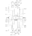
- FIG. 1 is a top view of the MEMS switch according to the first embodiment of the present invention.
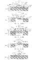
- 2 (S1) is a sectional view taken along line S1-S1 in FIG. 1
- FIG. 2 (S2) is a sectional view taken along line S2-S2 in FIG. 1
- FIG. 2 (S3) is taken along line S3-S3 in FIG. 2 is a sectional view taken along line S4-S4 in FIG. 1
- FIG. 2 (S5) is a sectional view taken along line S5-S5 in FIG. 3
- S6 is a sectional view taken along line S6-S6 in FIG.
- FIG. 3 (S7) is a sectional view taken along line S7-S7 in FIG. 1, and FIG.
- FIG. 4 is an explanatory diagram of a usage method and functions of the MEMS switch shown in FIG.
- FIG. 5 is an explanatory diagram of the usage and functions of the MEMS switch shown in FIG.
- FIG. 6 is a top view of the MEMS switch according to the second embodiment of the present invention.
- FIG. 7 is an explanatory diagram of a usage method and functions of the MEMS switch shown in FIG.
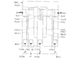
- FIG. 8 is a top view of the MEMS switch according to the third embodiment of the present invention.
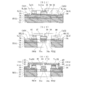
- FIG. 9 (S11) is a sectional view taken along line S11-S11 in FIG. 8
- FIG. 9 (S12) is a sectional view taken along line S12-S12 in FIG. 8
- FIG. 9 (S13) is taken along line S13-S13 in FIG.
- 10 (S14) is a sectional view taken along line S14-S14 in FIG. 8
- FIG. 10 (S15) is a sectional view taken along line S15-S15 in FIG. 8
- FIG. 10 (S16) is taken along line S16-S16 in FIG.
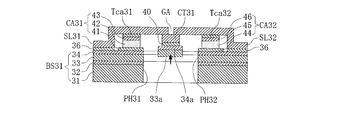
- FIG. 10 (S17) is a sectional view taken along line S17-S17 in FIG. 8, and FIG.
- FIG. 10 (S18) is a sectional view taken along line S18-S18 in FIG.
- FIG. 11 is an explanatory diagram of usage and functions of the MEMS switch shown in FIG.
- FIG. 12 is an explanatory diagram of the usage and functions of the MEMS switch shown in FIG.
- First Embodiment 1 to 5 show a first embodiment of the present invention (MEMS switch).
- MEMS switch the left, right, bottom, top, front, back, and back directions in FIG. 1 and the directions corresponding to these in the other drawings are respectively represented as front, back, left, right, top, and bottom. .
- the MEMS switch SD10 shown in FIGS. 1 to 3 has a multilayer structure created by using a known thin film forming method.
- the MEMS switch SD10 is configured to have a front-rear dimension of about 1.0 mm, a left-right dimension of about 2.0 mm, and a vertical dimension of about 0.5 mm.
- the MEMS switch SD10 includes a base BS11, a lever FL11, a contact electrode CT11, a first tunable capacitor CA11, a connection terminal Tca11, a second tunable capacitor CA12, a connection terminal Tca12, and a first signal line SL11.
- the base BS 11 is made of a first base layer 11 made of Si or the like, SiO 2 or the like, and A first insulator layer 12 formed on the first base layer 11 made of Si or the like, and, the second base layer 13 formed on the first insulator layer 11 made of SiO 2 or the like, and And a second insulator layer 14 formed on the second base layer 13.
- a first through hole PH11 having a substantially rectangular outline in top view is formed in the first base layer 11 and the first insulator layer 12.
- the second base layer 13 and the second insulator layer 14 are formed with two second through holes PH12 having a substantially rectangular outline in top view and a smaller front-rear dimension than the first through hole PH11 in parallel. ing. Between the two second through holes PH12, there are a band-shaped base layer 13a and a band-shaped insulator layer 14a which are base materials of the lever FL11.
- the lever FL11 may be operable by removing only the first insulator layer 12 without forming the first through hole PH11 in the first base layer 11.
- a pair of first electrode layers 15 made of Ti / Pt in which a Ti layer and a Pt layer are stacked and having a substantially rectangular outline in top view are formed.
- a pair of second electrode layers 16 made of Ti / Pt and having a substantially rectangular outline in top view are formed on the front upper surface and the rear upper surface of the base BS 11 with the same thickness as the first electrode layer 15. ing.
- the lever FL11 has two drive portions FL11a, a displacement portion FL11b located between the drive portions FL11a, and a hinge portion FL11c that connects each drive portion FL11a and the displacement portion FL11b.
- Each drive unit FL11a uses the left and right portions of the band-shaped base layer 13a and the band-shaped insulator layer 14a described above as its base material.
- a third electrode layer 17 made of Ti / Pt and having a substantially rectangular outline in top view is formed continuously with the first electrode layer 15 with the same thickness as the first electrode layer 15.
- a piezoelectric layer 18 made of PZT or the like and having the same top view contour as that of the third electrode layer 17 is formed.
- a fourth electrode layer 19 made of Ti / Pt and having the same top view contour as that of the piezoelectric layer 18 is formed on the piezoelectric layer 18.
- the displacement part FL11b uses the central part of the band-shaped base layer 13a and the band-shaped insulator layer 14a described above as its base material.
- a dummy electrode layer 20 made of Ti / Pt and having a substantially rectangular outline in top view has the same thickness as the third electrode layer 17 at the center in the front-rear direction of the center portion of the band-shaped base layer 13a and the band-shaped insulator layer 14a. Is formed.
- a dummy piezoelectric layer 21 made of PZT or the like and having the same top profile as the dummy electrode layer 20 is formed with the same thickness as the piezoelectric layer 18.
- a dummy electrode layer 22 made of Ti / Au in which a Ti layer and an Au layer are stacked and having the same top view outline as the dummy piezoelectric layer 21 is formed on the fourth electrode layer 19. They are formed with the same thickness. Further, on the dummy electrode layer 22, a contact electrode CT 11 made of Ti / Au and having the same top view contour as the dummy electrode layer 22 is formed.
- a lower electrode layer 23 made of Ti / Pt and having a substantially rectangular outline in top view is a dummy electrode layer 20 on the front side of the central portion of the band-shaped base layer 13a and the band-shaped insulator layer 14a constituting the displacement part FL11b. Are formed with the same thickness.
- a dielectric layer 24 made of PZT or the like and having the same top profile as the lower electrode layer 23 is formed with the same thickness as the dummy piezoelectric layer 21.
- the upper electrode layer 25 made of Ti / Pt and having the same top view contour as the dielectric layer 24 has the same thickness as the dummy electrode layer 22 or 0 than the dummy electrode layer 22.
- the lower electrode layer 23, the dielectric layer 24, and the upper electrode layer 25 constitute a first tunable capacitor CA11, and the first tunable capacitor CA11 is disposed on the displacement portion FL11b.
- a connection terminal Tca11 made of Ti / Au and having the same top view outline as the upper electrode layer 25 is formed on the upper electrode layer 25 of the first tunable capacitor CA11.
- the upper electrode layer connection terminal Tca11 is formed to have the same thickness as the contact electrode CT11 or slightly thinner than the contact electrode CT11 by about 0.01 ⁇ m to 0.5 ⁇ m.
- the height of the upper surface of the connection terminal Tca11 coincides with the height of the upper surface of the contact electrode CT11 or is slightly lower by about 0.01 ⁇ m to 0.5 ⁇ m.
- a lower electrode layer 26 made of Ti / Pt and having a substantially rectangular outline in top view is a dummy electrode layer on the rear side of the central portion of the band-shaped base layer 13a and the band-shaped insulator layer 14a constituting the displacement part FL11b.
- the same thickness as 20 is formed.
- a dielectric layer 27 made of PZT or the like and having the same top profile as the lower electrode layer 26 is formed with the same thickness as the dummy piezoelectric layer 21.
- the upper electrode layer 28 made of Ti / Pt and having the same top view contour as the dielectric layer 27 has the same thickness as the dummy electrode layer 22, or 0 than the dummy electrode layer 22.
- the lower electrode layer 26, the dielectric layer 27, and the upper electrode layer 28 constitute a second tunable capacitor CA12, and the second tunable capacitor CA12 is disposed on the displacement portion FL11b.
- a connection terminal Tca12 made of Ti / Au and having the same top view contour as that of the upper electrode layer 28 is formed on the upper electrode layer 28 of the second tunable capacitor CA12.
- the connection terminal Tca12 is formed to have the same thickness as the contact electrode CT11 or slightly thinner from about 0.01 ⁇ m to 0.5 ⁇ m.
- the height of the upper surface of the connection terminal Tca12 coincides with the height of the upper surface of the contact electrode CT11 or is slightly lower by about 0.01 ⁇ m to 0.5 ⁇ m.
- Each hinge portion FL11c uses as its base material a portion sandwiched between the front and rear portions and the central portion of the band-shaped base layer 13a and the band-shaped insulator layer 14a described above. By forming through holes (without reference numerals) in these base materials, each hinge portion FL11c is given flexibility to serve as a hinge. As can be seen from FIG. 1 and FIG. 3 (S8), the third electrode layer 17 on each drive portion FL11a is formed so as to reach the displacement portion FL11b via each hinge portion FL11c. The end of the layer 17 reaches both the lower electrode layer 23 of the first tunable capacitor CA11 and the lower electrode layer 26 of the second tunable capacitor CA12.
- the first signal line SL11 and the second signal line SL12 are made of Ti / Au, and have a cross-sectional shape in which a flat base material is bent 90 degrees and further bent 90 degrees in the opposite direction.
- the lower surface of the front portion of the first signal line SL11 is connected to the upper surface of the second electrode layer 16 on the front side
- the lower surface of the rear portion of the second signal line SL12 is connected to the upper surface of the second electrode layer 16 on the rear side.
- the first signal line SL11 and the second signal line SL12 are formed to be line symmetric with respect to the S8-S8 line, the upper and lower surfaces of the rear portion of the first signal line SL11 and the second signal line SL12 are formed.
- the upper and lower surfaces of the front portion of the are flush with each other.
- the left and right dimensions of the first signal line SL11 and the second signal line SL12 are larger than the left and right dimensions of the contact electrode CT11 and the connection terminals Tca11 and Tca12. Further, the rear portion of the first signal line SL11 and the front portion of the second signal line SL12 extend above the contact electrode CT11, and the first signal line SL11 and the front portion are between the rear portion and the front portion. A gap GA is provided for non-conduction with the second signal line SL12.
- the top surface heights of the contact electrode CT11, the connection terminal Tca11, and the connection terminal Tca12 are substantially the same, or the contact electrode CT11 is slightly higher than the connection terminal Tca11 or the connection terminal Tca12 by about 0.01 ⁇ m to 0.5 ⁇ m. Therefore, the lower surface of the rear portion of the first signal line SL11, the lower surface of the front portion of the second signal line SL12, and the contact electrode CT11, the lower surface of the rear portion of the first signal line SL11, and the connection terminal Between the upper surface of the Tca11 and between the lower surface of the front portion of the second signal line SL12 and the upper surface of the connection terminal Tca12, gaps (not shown) having substantially the same vertical dimension are formed.
- the ground terminal Tg11 is made of Ti / Au, and is formed on the left first electrode layer 15 so that the outline in top view is substantially rectangular.
- the ground terminal Tg12 is made of Ti / Au and is formed on the first electrode layer 15 on the right side so that the outline in top view is substantially rectangular.
- the drive voltage input terminal Ti11a is made of Ti / Au and is formed at the left end on the fourth electrode layer 19 of the left drive unit FL11a so that the outline in top view is substantially rectangular.
- the drive voltage input terminal Ti12a is made of Ti / Au and is formed at the right end on the fourth electrode layer 19 of the right drive unit FL11a so that the outline in top view is substantially rectangular.
- the bias voltage input terminal Ti11b is made of Ti / Au, and is formed on the upper surface on the left side of the base BS11 so that the outline in top view is substantially rectangular and is aligned with the drive voltage input terminal Ti11a.
- the bias voltage input terminal Ti12b is made of Ti / Au, and is formed on the right upper surface of the base BS11 so that the outline in top view is substantially rectangular and aligned with the drive voltage input terminal Ti12a. Yes.
- the bias voltage input terminal Ti11b and the front second electrode layer 16 are connected by a high resistance line HRL11, and the bias voltage input terminal Ti12b and the rear second electrode layer 16 are connected by a high resistance line HRL12. ing.
- These high resistance lines HRL11 and HRL12 are made of a high resistance material such as TaN, and have a higher resistivity than the first signal line SL11 and the second signal line SL12.
- the MEMS switch SD10 is mounted on a circuit board or the like as shown in FIG.
- the positive side of the first variable DC power source DC11a is connected to the drive voltage input terminal Ti11a
- the positive side of the second variable DC power source DC11b is connected to the bias voltage input terminal Ti11b
- the negative side of both the variable DC power sources DC11a and DC11b Is connected to the ground terminal Tg11.
- the positive side of the third variable DC power source DC12a is connected to the drive voltage input terminal Ti12a
- the positive side of the fourth variable DC power source DC11b is connected to the bias voltage input terminal Ti12b
- the negative side of both the variable DC power sources DC12a and DC12b Is connected to the ground terminal Tg11.
- one variable DC power supply can be commonly used for drive voltage application.
- one variable DC power supply different from the drive voltage application power supply is shared for bias voltage application. May be.
- the variable DC power supply may be replaced with a DC voltage input line provided on a circuit board or the like as long as voltage application described later can be performed in the same manner.
- a high-frequency signal line (input side) provided on a circuit board or the like is connected to the first signal line SL11, and a high-frequency signal line (output side) is connected to the second signal line SL12. Conversely, the high frequency signal line (input side) may be connected to the second signal line SL12, and the high frequency signal line (output side) may be connected to the first signal line SL11.
- a DC voltage of a predetermined value (hereinafter referred to as drive voltage) is applied from the first variable DC power supply DC11a to the drive voltage input terminal Ti11a, and this is applied to the drive voltage input terminal Ti12a from the third variable DC power supply DC12a.
- drive voltage a DC voltage of a predetermined value
- bias voltage a DC voltage of a predetermined value
- the drive voltage applied to the drive voltage input terminal Ti11a is applied to the piezoelectric layer 18 of the drive unit FL11a through the fourth electrode layer 19 constituting the drive unit FL11a on the left side of the lever FL11. Further, the drive voltage applied to the drive voltage input terminal Ti12a is applied to the piezoelectric layer 18 of the drive unit FL11a through the fourth electrode layer 19 constituting the drive unit FL11a on the right side of the lever FL11.
- the piezoelectric layer 18 constituting both the drive units FL11a contracts due to the piezoelectric effect. Due to the contraction of the piezoelectric layer 18, the hinge portion FL11c side of both the driving portions FL11a is warped upward, so that the displacement portion FL11b of the lever FL11 is displaced upward due to the warping, and the upper surface of the contact electrode CT11 is changed by the upward displacement. The lower surface of the rear portion of the first signal line SL11 and the lower surface of the front portion of the second signal line SL12 are contacted. By this contact, both signal lines SL11 and SL12 are brought into conduction through the contact electrode CT11. That is, the high-frequency signal input to the first signal line SL11 is output from the second signal line SL12 via the first signal line SL11, the contact electrode CT11, and the second signal line SL12.
- first tunable capacitor CA11 and the second tunable capacitor CA12 are disposed on the displacement portion FL11b of the lever FL11, and the lower surface of the rear portion of the first signal line SL11 and the front portion of the second signal line SL12 are disposed.
- connection terminal Tca11 of CA11 is in contact with and electrically connected to the lower surface of the rear portion of the first signal line SL11, and , The upper surface of the connection terminal Tca12 second tunable capacitor CA12 is electrically connected in contact with the lower surface of the front portion of the second signal line SL12.
- the bias voltage applied to the bias voltage input terminal Ti11b passes through the high resistance line HRL11, the front second electrode layer 16, the first signal line SL11, the connection terminal Tca11, and the upper electrode layer 25 of the first tunable capacitor CA11.
- the bias voltage applied to the bias voltage input terminal Ti12b is the high resistance line HRL12, the second electrode layer 16 on the rear side, the second signal line SL12, the connection terminal Tca12, and the upper electrode layer 28 of the second tunable capacitor CA12.
- the dielectric layer 27 of the second tunable capacitor CA12 Through the dielectric layer 27 of the second tunable capacitor CA12.
- the capacitances of both the tunable capacitors CA11 and CA11 are set so as to cancel the disturbance. If the bias voltage is changed, the characteristic impedance can be adjusted to an optimum value.
- the capacitance of both the tunable capacitors CA11 and CA11 is changed by the bias voltage so as to cancel the disturbance of the characteristic impedance that occurs during use. Since the characteristic impedance can be adjusted, the optimum characteristic impedance for the MEMS switch SD10 can be ensured. As a result, it is possible to avoid deterioration in characteristics such as an increase in transmission loss and a decrease in isolation caused by disturbance of characteristic impedance.
- the first tunable capacitor CA11 is provided corresponding to the first signal line SL11, and the second corresponding to the second signal line SL12. Since the two tunable capacitors CA12 are provided, the intended characteristic impedance adjustment is effectively performed on the entire line (the first signal line SL11, the contact electrode CT11, and the second signal line SL12) through which the high-frequency signal flows. Can do.
- the first tunable capacitor CA11 and the second tunable capacitor CA12 are disposed on the displacement portion FL11b of the lever FL11, and the first signal line A gap between the lower surface of the rear portion of SL11 and the lower surface of the front portion of the second signal line SL12 and the contact electrode CT11; a gap between the lower surface of the rear portion of the first signal line SL11 and the upper surface of the connection terminal Tca11; Since the gap between the lower surface of the front portion of the two-signal line SL12 and the upper surface of the connection terminal Tca12 is substantially the same, the upper surface of the contact electrode CT11 is moved upward by the displacement portion FL11b of the lever FL11.
- the first tuner is substantially simultaneously with the lower surface of the rear portion and the lower surface of the front portion of the second signal line SL12.
- the upper surface of the connection terminal Tca11 of the capacitor CA11 is brought into contact with and electrically connected to the lower surface of the rear portion of the first signal line SL11, and the upper surface of the connection terminal Tca12 of the second tunable capacitor CA12 is connected to the second signal line SL12. It can be made to contact and electrically connect to the lower surface of the front part.
- the first tunable capacitor CA11 is connected to the first signal line SL11 only when the first signal line SL11 and the second signal line SL12 become conductive through the contact electrode CT11, and the first The desired characteristic impedance can be adjusted by connecting the second tunable capacitor CA12 to the two-signal line SL12.
- the upper surface height of the contact electrode CT11 is slightly higher than the upper surface height of the connection terminal Tca11 and the upper surface height of the connection terminal Tca12 by about 0.01 ⁇ m to 0.5 ⁇ m, thereby making the first signal line SL11.
- the contact pressure between the lower surface of the rear portion and the lower surface of the front portion of the second signal line SL12 and the contact electrode CT11 is the contact pressure between the lower surface of the rear portion of the first signal line SL11 and the upper surface of the connection terminal Tca11. Since the contact pressure between the lower surface of the front portion of the two-signal line SL12 and the upper surface of the connection terminal Tca12 can be increased, the stability of the conduction state of the switch is improved.
- the bias voltage applied to the bias voltage input terminal Ti11b is applied to the dielectric layer 24 of the first tunable capacitor CA11 via the high resistance line HRL11.
- the bias voltage applied to the bias voltage input terminal Ti12b is applied to the dielectric layer 27 of the second tunable capacitor CA12 via the high resistance line HRL12, a high resistance is applied from the first signal line SL11.
- a high frequency signal leaks to the line HRL11 side, and a high frequency signal leaks from the second signal line SL12 to the high resistance line HRL12 side. Thereby, characteristic deterioration of the high frequency signal which flows via 1st signal track
- the contact electrode CT11 is in contact with the first signal line SL11 and the second signal line SL12, and the connection terminal Tca11 of the first tunable capacitor CA11.
- the connection terminal Tca11 of the first tunable capacitor CA11 Are in contact with or in proximity to the first signal line SL11 and the connection terminal Tca12 of the second tunable capacitor CA12 is in contact with or in proximity to the second signal line SL12, the tunables from the connection terminals Tca11 and Tca12.
- the MEMS switch SD10 according to the embodiment of the present invention is used in a mode in which the piezoelectric FL of the lever FL11 is not used in the conductive state of the switch by utilizing the latching state in which the contact continues even with the electrostatic attraction alone. You can also
- the MEMS switch SD10 can be regarded as a device having a filter function.
- the ability to vary the characteristic impedance means that the filter function can be varied. Since the two tunable capacitors CA11 and CA12 provided on both sides of the contact electrode CT11 are connected to the ground, the first signal line SL11 and the second signal line through which high-frequency signals pass through the tunable capacitors CA11 and CA12.
- a low-pass filter can be configured by combining with the inductance component of SL12. If the capacitances of the tunable capacitors CA11 and CA12 are changed, the cut-off frequency can be adjusted.
- the piezoelectric layer 18, the dummy piezoelectric layer 21, the dielectric layer 24 that configures the first tunable capacitor CA11, and the second tuner that configure each drive unit FL11a are respectively formed by PZT, but instead of PZT, lead zirconate, lead titanate, lead magnesium niobate, lead nickel niobate, barium titanate, Sodium bismuth titanate, potassium sodium niobate, strontium bismuth tantalate, and the like can be used.
- the first signal line SL11, the second signal line SL12, the ground terminals Tg11 and Tg12, the drive voltage input terminals Ti11a and Ti12a, and the bias voltage input terminals Ti11b and Ti12b are respectively Ti layers in which a Ti layer and a Pt layer are stacked.
- any one of a Cr layer, a Zr layer, a TiN layer, or a TiO 2 layer can be used instead of the Ti layer of Ti / Pt and / or Ti / Au.
- any one of an Au alloy layer, a Cu layer, and an Ag layer can be used instead of the Ti / Pt Pt layer.
- any one of an Au alloy layer, a Cu layer, and an Ag layer can be used instead of the Ti / Au Au layer.
- a single layer composed of a Pt layer, an Au layer, an Au alloy layer, a Cu layer, or an Ag layer may be used instead of Ti / Pt or Ti / Au.
- the thickness of the Ti layer, Cr layer, Zr layer, TiN layer, or TiO 2 layer can be 1 nm to 100 nm, and the Pt layer, Au layer, Au alloy layer, Cu
- the film thickness of the layer or the Ag layer can be 0.1 ⁇ m to 30 ⁇ m.
- the dummy electrode layer 20 is disposed on the displacement portion FL11b in order to align the upper surface height of the contact electrode CT11 with the upper surface height of the connection terminals Tca11 and Tca12.
- a dummy piezoelectric layer 21 and a dummy electrode layer 22 are formed, and a contact electrode CT11 is formed thereon.
- a thickness obtained by adding the thicknesses of the dummy piezoelectric layer 21 and the dummy electrode layer 22, or the dummy piezoelectric layer 21 and A contact electrode CT11 having a thickness obtained by adding about 0.01 ⁇ m to 0.5 ⁇ m to the thickness obtained by adding the thickness of the dummy electrode layer 22 may be formed on the dummy electrode layer 20.
- the thickness obtained by adding the thicknesses of the dummy electrode layer 20, the dummy piezoelectric layer 21, and the dummy electrode layer 22 is added. Can be formed on the strip-shaped insulator layer 14a.
- one ground terminal Tg11 is shared as the ground terminal of the left drive unit FL11a and the first tunable capacitor CA11, and the other one
- the ground terminal Tg12 is commonly used as the ground terminal of the right drive unit FL11a and the second tunable capacitor CA12.
- a ground terminal dedicated to the first tunable capacitor CA11 is separately provided, and this is connected to the lower electrode layer 23 of the first tunable capacitor CA11 via a dedicated line.
- a ground terminal may be provided separately and connected to the lower electrode layer 26 of the second tunable capacitor CA12 by a dedicated line.
- the bias voltage applied to the dielectric layer 24 of the first tunable capacitor CA11 and the bias voltage applied to the dielectric layer 27 of the second tunable capacitor CA12 can be made different. That is, the characteristic impedance adjustment for the first signal line SL11 side and the characteristic impedance adjustment for the second signal line SL12 side can be performed individually, so that finer characteristic impedance adjustment can be performed as a whole.
- FIG. 6 and 7 show a second embodiment of the present invention (MEMS switch).
- MEMS switch MEMS switch
- the MEMS switch SD20 shown in FIG. 6 has a multilayer structure created using a known thin film formation technique.
- the MEMS switch SD20 is configured to have a front-rear dimension of about 1.0 mm, a left-right dimension of about 1.2 mm, and a vertical dimension of about 0.5 mm.
- the MEMS switch SD20 includes the MEMS switch SD10, A point using a base BS11 ′ having a smaller left and right dimension than the base BS11.
- a first through hole PH1 having a smaller left and right dimension than the first through hole PH11 and the second through hole PH12. 1 'and the second through-hole PH12' are used to make the top through-line contour of the second through-hole PH12 'substantially U-shaped, with the drive unit FL11a and the hinge FL11c on the right side of the lever FL11 removed.
- the point used as the bar FL11 ′, the first electrode layer 15 provided on the right side of the base BS11, and the drive voltage input terminal Ti12a The bias voltage input terminal 12b, the ground terminal Tg12, and the high resistance line HRL12 are eliminated, and a bias voltage input terminal Ti11c that replaces the bias voltage input terminal 12b is provided on the left side of the base BS11 ′.
- High resistance line HR The configuration is different in that L12 ′ is provided on the left side of the second signal line SL12. Since the other configuration of the MEMS switch SD20 is the same as that of the MEMS switch SD10, the description thereof is omitted.
- the MEMS switch SD20 is mounted on a circuit board or the like as shown in FIG. Further, the positive side of the first variable DC power source DC11a is connected to the drive voltage input terminal Ti11a, the positive side of the second variable DC power source DC11b is connected to the bias voltage input terminal Ti11b, and the positive side of the third variable DC power source DC11c is connected. The bias voltage input terminal Ti11c is connected, and the negative sides of these variable DC power supplies DC11a, DC11b, and DC11c are connected to the ground terminal Tg11.
- variable DC power supply can be shared for bias voltage application.
- the variable DC power supply may be replaced with a DC voltage input line provided on a circuit board or the like as long as voltage application described later can be performed in the same manner.
- the high frequency signal line (input side) provided on the circuit board or the like is connected to the first signal line SL11, and the high frequency signal line (output side) is connected to the second signal line SL12.
- the high frequency signal line (input side) may be connected to the second signal line SL12, and the high frequency signal line (output side) may be connected to the first signal line SL11.
- a predetermined direct-current voltage (hereinafter referred to as drive voltage) is applied from the first variable direct-current power source DC11a to the drive voltage input terminal Ti11a. Further, a DC voltage of a predetermined value (hereinafter referred to as a bias voltage) is applied from the second variable DC power supply DC11b to the bias voltage input terminal Ti11b, and the same as this from the third variable DC power supply DC11c to the bias voltage input terminal Ti11c. A value bias voltage is applied.
- the operation and effect of the MEMS switch SD20 are the same as the operation and effect of the MEMS switch SD10.
- FIG. 8 to 12 show a third embodiment of the present invention.
- the left, right, bottom, top, front, back and back of FIG. Indicated as right, top and bottom.
- the MEMS switch SD30 shown in FIGS. 8 to 10 has a multilayer structure created by using a known thin film forming method.
- the MEMS switch SD30 is configured to have a front-rear dimension of about 1.0 mm, a left-right dimension of about 1.20 mm, and a vertical dimension of about 0.5 mm.
- the MEMS switch SD30 includes a base BS31, a lever FL31, a contact electrode CT31, a first tunable capacitor CA31, a connection terminal Tca31, a second tunable capacitor CA32, a connection terminal Tca32, and a first signal line SL31.
- the base BS 31 is made of a first base layer 31 made of Si or the like, SiO 2 or the like, and A first insulator layer 32 formed on the first base layer 31 made of Si or the like, and, the second base layer 33 formed on the third insulating layer 31 made of SiO 2 or the like, and And a second insulator layer 34 formed on the second base layer 33.
- first through hole PH31 having a substantially rectangular outline in top view is formed.
- second base layer 33 and the second insulator layer 34 are formed with a second through hole PH32 having a substantially U-shaped outline in top view, and the mother of the lever FL31 is formed inside the second through hole PH32.
- a band-shaped base layer 33a and a band-shaped insulator layer 34a serving as materials are present.
- a first electrode layer 35 made of Ti / Pt and having a substantially rectangular outline in top view is formed on the upper left surface of the base BS31. Further, on the front upper surface and the rear upper surface of the base BS 11, a second electrode layer 36 made of Ti / Pt and having a substantially rectangular outline in top view is formed with the same thickness as the first electrode layer 35.
- the lever FL31 has a drive part FL31a, a displacement part FL31b located at the free end of the drive part FL31a, and a hinge part FL31c connecting the drive part FL31a and the displacement part FL31b.
- the drive unit FL31a uses the left part of the band-shaped base layer 33a and the band-shaped insulator layer 34a described above as its base material.
- a third electrode layer 37 made of Ti / Pt and having a substantially rectangular outline in top view is formed continuously with the first electrode layer 35 with the same thickness as the first electrode layer 35.
- a piezoelectric layer 38 made of PZT or the like and having the same top view contour as the third electrode layer 37 is formed.
- a fourth electrode layer 39 made of Ti / Pt and having the same top view contour as that of the piezoelectric layer 38 is formed on the piezoelectric layer 38.
- the displacement part FL31b uses the right end portion of the band-shaped base layer 33a and the band-shaped insulator layer 34a described above as its base material.
- a dummy electrode layer 40 made of Ti / Pt and having a substantially rectangular outline in top view is formed with the same thickness as the third electrode layer 37. ing.
- a contact electrode CT31 made of Ti / Au and having the same top view contour as the dummy electrode layer 40 is formed.
- Hinge portion FL31c uses as its base material the portion sandwiched between the left and right end portions of band-shaped base layer 33a and band-shaped insulator layer 34a described above. By forming through holes (without reference numerals) in these base materials, the hinge portion FL31c is given flexibility to serve as a hinge.
- a lower electrode layer 41 made of Ti / Pt and having a substantially rectangular outline in top view is formed in the same thickness as the third electrode layer 37 on the front side of the second through hole PH32 on the base BS31.
- a dielectric layer 42 made of PZT or the like and having the same outline as the lower electrode layer 41 in a top view is formed with the same thickness as the piezoelectric layer 38.
- an upper electrode layer 43 made of Ti / Pt and having the same top profile as the dielectric layer 42 is formed on the dielectric layer 42 with the same thickness as the fourth electrode layer 39.
- the lower electrode layer 41, the dielectric layer 42, and the upper electrode layer 43 constitute a first tunable capacitor CA31, and the first tunable capacitor CA31 is disposed on the base BS31. Further, on the upper electrode layer 43 of the first tunable capacitor CA31, a connection terminal Tca31 made of Ti / Au and having the same top view outline as the upper electrode layer 43 is formed. As can be seen from FIG. 9 (S13), the upper surface of the connection terminal Tca31 is in close contact with and electrically connected to the lower surface of the rear portion of the first signal line SL31.
- a lower electrode layer 44 made of Ti / Pt and having a substantially rectangular outline in top view is formed with the same thickness as the third electrode layer 37. Yes.
- a dielectric layer 45 made of PZT or the like and having the same outline as the lower electrode layer 44 in the top view is formed with the same thickness as the piezoelectric layer 38.
- an upper electrode layer 46 made of Ti / Pt and having the same top view contour as the dielectric layer 45 is formed on the dielectric layer 45 with the same thickness as the fourth electrode layer 39.
- the lower electrode layer 44, the dielectric layer 44 and the upper electrode layer 45 constitute a second tunable capacitor CA32, and the second tunable capacitor CA32 is disposed on the base BS31. Further, on the upper electrode layer 446 of the second tunable capacitor CA32, a connection terminal Tca32 made of Ti / Au and having the same top view outline as the upper electrode layer 46 is formed. As can be seen from FIG. 9 (S13), the upper surface of the connection terminal Tca31 is in close contact with and electrically connected to the lower surface of the front portion of the second signal line SL32.
- the first signal line SL31 and the second signal line SL32 are made of Ti / Au and have a cross-sectional shape in which a flat base material is bent 90 degrees and further bent 90 degrees in the opposite direction.
- the lower surface of the front portion of the first signal line SL31 is connected to the upper surface of the second electrode layer 36 on the front side, and the lower surface of the rear portion of the second signal line SL32 is connected to the upper surface of the second electrode layer 36 on the rear side.
- first signal line SL31 and the second signal line SL32 are formed so as to be line-symmetric with respect to the S16-S16 line in the front-rear direction, the upper and lower surfaces of the rear portion of the first signal line SL31 and the second The upper and lower surfaces of the front portion of the signal line SL32 are flush with each other.
- the left and right dimensions of the first signal line SL31 and the second signal line SL32 are larger than the left and right dimensions of the contact electrode CT31 and the connection terminals Tca31 and Tca32.
- the rear part of the first signal line SL31 and the front part of the second signal line SL32 extend above the contact electrode CT31, and the first signal line SL31 and the front part are between the rear part and the front part.
- a gap GA is provided to make the second signal line SL32 non-conductive.
- a gap (no symbol) having a predetermined vertical dimension is formed between the lower surface of the rear portion of the first signal line SL31 and the lower surface of the front portion of the second signal line SL32 and the contact electrode CT31.
- the ground terminal Tg31 is made of Ti / Au and is formed on the first electrode layer 35 so that the outline in top view is substantially rectangular.
- the drive voltage input terminal Ti31a is made of Ti / Au, and is formed at the left end on the fourth electrode layer 39 of the drive unit FL31a so that the outline in top view is substantially rectangular.
- the bias voltage input terminal Ti31b is made of Ti / Au, and is formed on the upper surface on the left front side of the base BS31 so that the outline in top view is substantially rectangular and is aligned with the ground terminal Tg31 at an interval.
- the bias voltage input terminal Ti31c is made of Ti / Au, and is formed on the upper left rear surface of the base BS11 so that the outline in a top view is substantially rectangular and is aligned with the drive voltage input terminal Ti31a. Yes.
- the bias voltage input terminal Ti31b and the front second electrode layer 36 are connected by a high resistance line HRL31, and the bias voltage input terminal Ti31c and the rear second electrode layer 36 are connected by a high resistance line HRL32. ing.
- These high resistance lines HRL31 and HRL32 are made of a high resistance material such as TaN, and have higher resistivity than the first signal line SL31 and the second signal line SL32.
- the MEMS switch SD30 is mounted on a circuit board or the like as shown in FIG.
- the positive side of the first variable DC power source DC31a is connected to the drive voltage input terminal Ti31a
- the positive side of the second variable DC power source DC31b is connected to the bias voltage input terminal Ti31b
- the positive side of the third variable DC power source DC31c is connected.
- the bias voltage input terminal Ti31c is connected, and the negative sides of these variable DC power supplies DC31a, DC31b and DC31c are connected to the ground terminal Tg31.
- variable DC power sources DC31a, DC31b, and DC31c are shown in the drawing, the bias voltages applied to the bias voltage input terminals Ti31b and Ti31c have the same value as will be described later.
- the variable DC power supply can be shared for driving voltage application.
- the variable DC power supply may be replaced with a DC voltage input line provided on a circuit board or the like as long as voltage application described later can be performed in the same manner.
- the high frequency signal line (input side) provided on the circuit board or the like is connected to the first signal line SL31, and the high frequency signal line (output side) is connected to the second signal line SL32.
- the high frequency signal line (input side) may be connected to the second signal line SL32, and the high frequency signal line (output side) may be connected to the first signal line SL31.
- a predetermined direct current voltage (hereinafter referred to as drive voltage) is applied from the first variable direct current power source DC31a to the drive voltage input terminal Ti31a.
- a DC voltage of a predetermined value (hereinafter referred to as a bias voltage) is applied from the second variable DC power source DC31b to the bias voltage input terminal Ti31b, and the same as this from the third variable DC power source DC31c to the bias voltage input terminal Ti31c.
- a value bias voltage is applied.
- the drive voltage applied to the drive voltage input terminal Ti31a is applied to the piezoelectric layer 38 of the drive unit FL31a through the fourth electrode layer 39 constituting the drive unit FL31a of the lever FL31.
- the piezoelectric layer 38 constituting the drive unit FL31a contracts due to the piezoelectric effect. Due to the contraction of the piezoelectric layer 38, the hinge portion FL31c side of the driving portion FL31a is warped upward, and the warping rise displaces the displacement portion FL31b of the lever FL31, and the upper displacement causes the upper surface of the contact electrode CT31 to be the first signal.
- the lower surface of the rear portion of the line SL31 and the lower surface of the front portion of the second signal line SL32 are contacted, and the contact causes both signal lines SL31 and SL32 to be in a conductive state via the contact electrode CT31. That is, the high-frequency signal input to the first signal line SL31 is output from the second signal line SL32 via the first signal line SL31, the contact electrode CT31, and the second signal line SL32.
- the bias voltage applied to the bias voltage input terminal Ti31b passes through the high resistance line HRL31, the second electrode layer 36 on the front side, the first signal line SL31, the connection terminal Tca31, and the upper electrode layer 43 of the first tunable capacitor CA31.
- the bias voltage applied to the bias voltage input terminal Ti31c is the high resistance line HRL32, the second electrode layer 36 on the rear side, the second signal line SL32, the connection terminal Tca32, and the upper electrode layer 46 of the second tunable capacitor CA32.
- the dielectric layer 45 of the second tunable capacitor CA32 Through the dielectric layer 45 of the second tunable capacitor CA32.
- the capacitances of both the tunable capacitors CA31 and CA31 are set so as to cancel the disturbance. If the bias voltage is changed, the characteristic impedance can be adjusted to an optimum value.
- the capacitance of both the tunable capacitors CA31 and CA31 is changed by the bias voltage so as to cancel the disturbance of the characteristic impedance that occurs during use. Since the characteristic impedance can be adjusted, an optimum characteristic impedance can be ensured for the MEMS switch SD30, thereby avoiding deterioration in characteristics such as an increase in transmission loss and a decrease in isolation due to the disturbance of the characteristic impedance.
- the first tunable capacitor CA31 is provided corresponding to the first signal line SL31, and the first tunable capacitor CA31 is provided corresponding to the second signal line SL32. Since the two tunable capacitors CA32 are provided, the desired characteristic impedance adjustment is effectively performed on the entire line (the first signal line SL31, the contact electrode CT31, and the second signal line SL32) through which the high-frequency signal flows. Can do.
- the first tunable capacitor CA31 and the second tunable capacitor CA32 are arranged on the base BS31, and the upper surface of the connection terminal Tca31 on the first tunable capacitor CA31 is the first.
- One signal line SL31 is in contact with and electrically connected to the lower surface of the rear portion, and the upper surface of the connection terminal Tca32 on the second tunable capacitor CA32 is in contact with the lower surface of the front portion of the second signal line SL32.
- the first tunable capacitor CA31 and the connection terminal Tca31 can play the role of a column that supports and holds the rear portion of the first signal line SL31, and the second tunable The capacitor CA32 and the connection terminal Tca32 support and hold the front portion of the second signal line SL32. It is possible to play a role of that post.
- the contact electrode CT31 since the rear portion of the first signal line SL31 and the front portion of the second signal line SL32 that are in contact with the contact electrode CT31 can be reinforced, the contact electrode CT31 repeatedly contacts and cancels these portions. However, it is difficult for the portion to be deformed, and contact failure that may occur due to the deformation can be prevented.
- the bias voltage applied to the bias voltage input terminal Ti31b is applied to the dielectric layer 42 of the first tunable capacitor CA31 via the high resistance line HRL31.
- the bias voltage applied to the bias voltage input terminal Ti31c is applied to the dielectric layer 45 of the second tunable capacitor CA32 via the high resistance line HRL32, the high resistance is applied from the first signal line SL31.
- a high frequency signal leaks to the line HRL31 side and a high frequency signal leaks from the second signal line SL32 to the high resistance line HRL32 side. Thereby, characteristic deterioration of the high frequency signal which flows via 1st signal track
- the MEMS switch SD30 can be regarded as a device having a filter function. That the characteristic impedance can be made variable means that the filter function can be made variable. Since the two tunable capacitors CA31 and CA32 provided on both sides of the contact electrode CT31 are connected to the ground, the first signal line SL31 and the second signal line SL32 through which the high-frequency signal passes through the tunable capacitors CA31 and CA32. A low-pass filter can be configured by combining with an inductance component. If the capacitances of the tunable capacitors CA31 and CA32 are changed, the cut-off frequency can be adjusted.
- the dielectric material layer which comprises the piezoelectric material layer 38 which comprises the drive part FL31a, the dielectric material layer 42 which comprises 1st tunable capacitor CA31, and 2nd tunable capacitor CA32 The body layer 45 is formed of PZT, but instead of PZT, lead zirconate, lead titanate, lead magnesium niobate, lead nickel niobate, barium titanate, sodium bismuth titanate, niobate Potassium sodium, strontium bismuth tantalate, or the like can be used.
- the first electrode layer 35, the second electrode layer 36, the third electrode layer 37 and the fourth electrode layer 39 constituting the driving unit FL11a, and the dummy electrode layer 40.
- the first signal line SL31, the second signal line SL32, the ground terminal Tg31, the drive voltage input terminal Ti31a, and the bias voltage input terminals Ti31b and Ti31c are respectively Ti / Pt or Ti in which a Ti layer and a Pt layer are stacked.
- any one of a Cr layer, a Zr layer, a TiN layer, or a TiO 2 layer can be used instead of the Ti layer of Ti / Pt and / or Ti / Au.
- any one of an Au alloy layer, a Cu layer, and an Ag layer can be used instead of the Ti / Pt Pt layer.
- any one of an Au alloy layer, a Cu layer, and an Ag layer can be used instead of the Ti / Au Au layer.
- a single layer composed of a Pt layer, an Au layer, an Au alloy layer, a Cu layer, or an Ag layer may be used instead of Ti / Pt or Ti / Au.
- the thickness of the Ti layer, Cr layer, Zr layer, TiN layer, or TiO 2 layer can be 1 nm to 100 nm, and the Pt layer, Au layer, Au alloy layer, Cu
- the film thickness of the layer or the Ag layer can be 0.1 ⁇ m to 30 ⁇ m.
- one ground terminal Tg31 is shared as the ground terminal of the drive unit FL31a, the first tunable capacitor CA31, and the second tunable capacitor CA32.
- a ground terminal dedicated to the tunable capacitor CA31 is separately provided, and this is connected to the lower electrode layer 41 of the first tunable capacitor CA31 by a dedicated line, and a ground terminal dedicated to the second tunable capacitor CA32 is separately provided.
- the lower electrode layer 44 of the two tunable capacitor CA32 may be connected by a dedicated line.
- the bias voltage applied to the dielectric layer 42 of the first tunable capacitor CA31 can be made different from the bias voltage applied to the dielectric layer 45 of the second tunable capacitor CA32. That is, the characteristic impedance adjustment for the first signal line SL31 side and the characteristic impedance adjustment for the second signal line SL32 side can be performed individually, so that finer characteristic impedance adjustment can be performed as a whole.
Landscapes
- Engineering & Computer Science (AREA)
- Power Engineering (AREA)
- Microelectronics & Electronic Packaging (AREA)
- Manufacturing & Machinery (AREA)
- Micromachines (AREA)
Abstract
【課題】使用時に生じ得る特性インピーダンスの乱れを相殺するように該特性インピーダンスを調整できるMEMSスイッチを提供する。 【解決手段】MEMSスイッチSD10は、第1信号線路SL11に対応して設けられた第1チューナブルキャパシタCA11と、第2信号線路SL12に対応して設けられた第2チューナブルキャパシタCA12と、第1信号線路SL11及び第1チューナブルキャパシタCA11の一方の電極層25側を通じて該第1チューナブルキャパシタCA11の誘電体層24にバイアス電圧を印加するためのバイアス電圧入力端子Ti11bと、第2信号線路SL12及び第2チューナブルキャパシタCA12の一方の電極層28側を通じて該第2チューナブルキャパシタCA12の誘電体層27にバイアス電圧を印加するためのバイアス電圧入力端子Ti12bと、を備える。
Description
本発明は、MEMS(Micro Electro Mechanical Systems)スイッチに関する。
ダイオードやFET等を用いた半導体スイッチは周波数が高くなるに従って伝送損失増加やアイソレーション低下等の特性悪化を生じるが、MEMSスイッチはこのような特性悪化を生じ難いことから、高周波回路、例えば数GHz~数百GHzの高周波信号が流れる回路に用いるのに好適なスイッチングデバイスとして着目されている。
一般に、MEMSスイッチは、公知の薄膜形成手法を用いて作成された多層構造を有している。一般のMEMSスイッチは、非導通の第1信号線路及び第2信号線路に接点電極を接触させることで両信号線路を接点電極を介して導通状態とし、また、両信号線路に対する接点電極の接触を解くことで両信号線路を非導通状態とする機能を有している。
MEMSスイッチは、例えば50Ωや75Ω等の所定の特性インピーダンスを有するように設計されるが、特に高周波回路に用いるとその特性インピーダンスが外的影響によって乱れてしまうことがある。
この特性インピーダンスの乱れはMEMSスイッチの用途に応じてある程度推測することは可能であるが、信号線路構造(線路幅や線路長や線路厚さ等)を調整する等して推測結果に基づいて特性インピーダンスを予め調整しておいても、実際には不測の外的影響も生じ得るため、最適な特性インピーダンスを確保することは難しい。また、用途毎に信号線路構造が異なるMEMSスイッチを製造することは、汎用性の面やコスト低減の面からして好ましいとは言えない。
換言すれば、使用時に生じ得る特性インピーダンスの乱れを相殺するように該特性インピーダンスを調整できるようにすれば、如何様な用途であってもMEMSスイッチに最適な特性インピーダンスを確保することができ、これにより特性インピーダンスの乱れを原因とした伝送損失増加やアイソレーション低下等の特性悪化を回避することができる。
本発明の目的は、使用時に生じ得る特性インピーダンスの乱れを相殺するように該特性インピーダンスを調整できるMEMSスイッチを提供することにある。
前記目的を達成するため、本発明は、非導通の第1信号線路及び第2信号線路に接点電極を接触させることで両信号線路を接点電極を介して導通状態とし、また、両信号線路に対する接点電極の接触を解くことで両信号線路を非導通状態とするMEMSスイッチであって、該MEMSスイッチは、第1信号線路に対応して設けられた第1チューナブルキャパシタと、第2信号線路に対応して設けられた第2チューナブルキャパシタと、第1信号線路及び第1チューナブルキャパシタの一方の電極層側を通じて該第1チューナブルキャパシタの誘電体層にバイアス電圧を印加するための第1バイアス電圧入力端子と、第2信号線路及び第2チューナブルキャパシタの一方の電極層側を通じて該第2チューナブルキャパシタの誘電体層にバイアス電圧を印加するための第1バイアス電圧入力端子と、を備える。
このMEMSスイッチによれば、第1チューナブルキャパシタの誘電体層と第2チューナブルキャパシタの誘電体層にバイアス電圧を印加することによって、両チューナブルキャパシタの誘電体層の比誘電率を変化させ、該変化によって両チューナブルキャパシタのキャパシタンスを変化させ、該変化によってMEMSスイッチの特性インピーダンスを変化させることができる。
つまり、回路基板等に搭載されたMEMSスイッチの特性インピーダンス(例えば50Ωや75Ω等)が外的影響によって乱れてしまう場合でも、該乱れを相殺するように両チューナブルキャパシタのキャパシタンスをバイアス電圧により変化させれば、該特性インピーダンスを最適な値に調整することができる。
本発明の様々な実施形態によれば、使用時に生じる特性インピーダンスの乱れを相殺するように該特性インピーダンスを調整できるので、MEMSスイッチに最適な特性インピーダンスを確保することができ、これにより特性インピーダンスの乱れを原因とした伝送損失増加やアイソレーション低下等の特性悪化を回避することができる。
本発明の上述した目的とそれ以外の目的と、構成特徴と、作用効果は、以下の説明と添付図面によって明らかとなる。
[第1実施形態]
図1~図5は本発明(MEMSスイッチ)の第1実施形態を示す。ここでの説明では、説明の便宜上、図1の左,右,下,上,手前及び奥と他の図のこれらに相当する方向をそれぞれ前,後,左,右,上及び下と表記する。
図1~図5は本発明(MEMSスイッチ)の第1実施形態を示す。ここでの説明では、説明の便宜上、図1の左,右,下,上,手前及び奥と他の図のこれらに相当する方向をそれぞれ前,後,左,右,上及び下と表記する。
先ず、図1~図3を参照して、MEMSスイッチSD10の構成について説明する。
図1~図3に示したMEMSスイッチSD10は、公知の薄膜形成手法を用いて作成された多層構造を有している。一実施形態において、このMEMSスイッチSD10は、前後寸法が約1.0mm、左右寸法が約2.0mm,上下寸法が約0.5mmに構成される。
このMEMSスイッチSD10は、ベースBS11と、レバーFL11と、接点電極CT11と、第1チューナブルキャパシタCA11と、接続端子Tca11と、第2チューナブルキャパシタCA12と、接続端子Tca12と、第1信号線路SL11と、第2信号線路SL12と、グランド端子Tg11及びTg12と、駆動電圧入力端子Ti11a及びTi12aと、バイアス電圧入力端子Ti11b及びTi12bと、を備えている。
ベースBS11は、Si等から成る第1ベース層11と、SiO2等から成り、且つ、
第1ベース層11上に形成された第1絶縁体層12と、Si等から成り、且つ、第1絶縁体層11上に形成された第2ベース層13と、SiO2等から成り、且つ、第2ベース層
13上に形成された第2絶縁体層14と、を有している。
第1ベース層11上に形成された第1絶縁体層12と、Si等から成り、且つ、第1絶縁体層11上に形成された第2ベース層13と、SiO2等から成り、且つ、第2ベース層
13上に形成された第2絶縁体層14と、を有している。
第1ベース層11及び第1絶縁体層12には、上面視輪郭が略矩形の第1貫通孔PH11が形成されている。また、第2ベース層13及び第2絶縁体層14には、上面視輪郭が略矩形で、且つ、第1貫通孔PH11よりも前後寸法が小さな2つの第2貫通孔PH12が平行に形成されている。この2つの第2貫通孔PH12の間にはレバーFL11の母材となる帯状ベース層13a及び帯状絶縁体層14aが存する。一実施形態においては、第1ベース層11に第1貫通孔PH11を形成せずに第1絶縁体層12のみ除去することで、レバーFL11を動作可能にしてもよい。
さらに、ベースBS11の左側上面と右側上面には、Ti層とPt層とを積層したTi/Ptから成り、且つ、上面視輪郭が略矩形の一組の第1電極層15が形成されている。さらに、ベースBS11の前側上面と後側上面には、Ti/Ptから成り、且つ、上面視輪郭が略矩形の一組の第2電極層16が第1電極層15と同じ厚さで形成されている。
レバーFL11は、2つの駆動部FL11aと、両駆動部FL11aの間に位置する変位部FL11bと、各駆動部FL11aと変位部FL11bとを結ぶヒンジ部FL11cと、を有している。
各駆動部FL11aは、先に述べた帯状ベース層13a及び帯状絶縁体層14aの左右部分をその母材とする。この左右部分上には、Ti/Ptから成り、且つ、上面視輪郭が略矩形の第3電極層17が第1電極層15と同じ厚さで該第1電極層15と連続して形成されている。また、第3電極層17上には、PZT等から成り、上面視輪郭が第3電極層17と同じ圧電体層18が形成されている。さらに、圧電体層18上には、Ti/Ptから成り、且つ、上面視輪郭が圧電体層18と同じ第4電極層19が形成されている。
変位部FL11bは、先に述べた帯状ベース層13a及び帯状絶縁体層14aの中央部分をその母材とする。この帯状ベース層13a及び帯状絶縁体層14aの中央部分の前後方向の中央には、Ti/Ptから成り、且つ、上面視輪郭が略矩形のダミー電極層20が第3電極層17と同じ厚さで形成されている。また、ダミー電極層20上には、PZT等から成り、且つ、上面視輪郭がダミー電極層20と同じダミー圧電体層21が圧電体層18と同じ厚さで形成されている。さらに、ダミー圧電体層21上には、Ti層とAu層とを積層したTi/Auから成り、且つ、上面視輪郭がダミー圧電体層21と同じダミー電極層22が第4電極層19と同じ厚さで形成されている。さらに、ダミー電極層22上には、Ti/Auから成り、且つ、上面視輪郭がダミー電極層22と同じ接点電極CT11が形成されている。
また、変位部FL11bを構成する帯状ベース層13a及び帯状絶縁体層14aの中央部分の前側には、Ti/Ptから成り、且つ、上面視輪郭が略矩形の下部電極層23がダミー電極層20と同じ厚さで形成されている。また、下部電極層23上には、PZT等から成り、且つ、上面視輪郭が下部電極層23と同じ誘電体層24がダミー圧電体層21と同じ厚さで形成されている。さらに、誘電体層24上には、Ti/Ptから成り、且つ、上面視輪郭が誘電体層24と同じ上部電極層25がダミー電極層22と同じ厚さか、又はダミー電極層22よりも0.01μm~0.5μm程度わずかに薄く形成されている。ここでの下部電極層23,誘電体層24及び上部電極層25は、第1チューナブルキャパシタCA11を構成しており、該第1チューナブルキャパシタCA11は変位部FL11b上に配置されている。さらに、第1チューナブルキャパシタCA11の上部電極層25上には、Ti/Auから成り、且つ、上面視輪郭が上部電極層25と同じ接続端子Tca11が形成されている。この上部電極層接続端子Tca11は、接点電極CT11と同じ厚さか、又は接点電極CT11よりも0.01μm~0.5μm程度わずかに薄く形成されている。図2(S3)から分かるように、この接続端子Tca11の上面高さは接点電極CT11の上面高さと一致しているか、又は0.01μm~0.5μm程度わずかに低くなっている。
また、変位部FL11bを構成する帯状ベース層13a及び帯状絶縁体層14aの中央部分の後側には、Ti/Ptから成り、且つ、上面視輪郭が略矩形の下部電極層26がダミー電極層20と同じ厚さで形成されている。また、下部電極層26上には、PZT等から成り、且つ、上面視輪郭が下部電極層26と同じ誘電体層27がダミー圧電体層21と同じ厚さで形成されている。さらに、誘電体層27上には、Ti/Ptから成り、且つ、上面視輪郭が誘電体層27と同じ上部電極層28がダミー電極層22と同じ厚さか、又はダミー電極層22よりも0.01μm~0.5μm程度わずかに薄く形成されている。ここでの下部電極層26,誘電体層27及び上部電極層28は、第2チューナブルキャパシタCA12を構成しており、該第2チューナブルキャパシタCA12は変位部FL11b上に配置されている。さらに、第2チューナブルキャパシタCA12の上部電極層28上には、Ti/Auから成り、且つ、上面視輪郭が上部電極層28と同じ接続端子Tca12が形成されている。この接続端子Tca12は、接点電極CT11と同じ厚さか、又は0.01μm~0.5μm程度わずかに薄く形成されている。図2(S3)から分かるように、この接続端子Tca12の上面高さは接点電極CT11の上面高さと一致しているか、又は0.01μm~0.5μm程度わずかに低くなっている。
各ヒンジ部FL11cは、先に述べた帯状ベース層13a及び帯状絶縁体層14aの前後部分と中央部分とに挟まれる部分をその母材とする。これらの母材に貫通孔(符号無し)を形成することで、各ヒンジ部FL11cに、ヒンジの役割を為す可撓性が付与されている。図1及び図3(S8)から分かるように、各駆動部FL11a上の第3電極層17は各ヒンジ部FL11c上を経由して変位部FL11bに及ぶように形成されていて、各第3電極層17の端は第1チューナブルキャパシタCA11の下部電極層23と第2チューナブルキャパシタCA12の下部電極層26の両方に達している。
第1信号線路SL11及び第2信号線路SL12は、Ti/Auから成り、平坦な母材料を90度屈曲させ、さらに逆方向に90度屈曲させた断面形状をそれぞれ有している。第1信号線路SL11の前側部分の下面は前側の第2電極層16の上面に接続され、第2信号線路SL12の後側部分の下面は後側の第2電極層16の上面に接続されている。第1信号線路SL11と第2信号線路SL12とがS8-S8線に対して線対称になるように形成されているため、第1信号線路SL11の後側部分の上下面と第2信号線路SL12の前側部分の上下面は面一になっている。
また、図1から分かるように、第1信号線路SL11及び第2信号線路SL12の左右寸法は、接点電極CT11と両接続端子Tca11及びTca12の左右寸法よりも大きい。さらに、第1信号線路SL11の後側部分と第2信号線路SL12の前側部分は接点電極CT11の上方まで延びていて、該後側部分と該前側部分との間には第1信号線路SL11と第2信号線路SL12とを非導通とするための隙間GAが設けられている。
さらに、接点電極CT11、接続端子Tca11、及び接続端子Tca12の上面高さは互いにほぼ同じか、又は接点電極CT11が接続端子Tca11又は接続端子Tca12よりも0.01μm~0.5μm程度わずかに高くなっていることから、第1信号線路SL11の後側部分の下面及び第2信号線路SL12の前側部分の下面と接点電極CT11との間と、第1信号線路SL11の後側部分の下面と接続端子Tca11の上面との間と、第2信号線路SL12の前側部分の下面と接続端子Tca12の上面との間には、ほぼ同一上下寸法の隙間(符号無し)が形成されている。
グランド端子Tg11は、Ti/Auから成り、左側の第1電極層15上に上面視輪郭が略矩形となるように形成されている。また、グランド端子Tg12は、Ti/Auから成り、右側の第1電極層15上に上面視輪郭が略矩形となるように形成されている。
駆動電圧入力端子Ti11aは、Ti/Auから成り、左側の駆動部FL11aの第4電極層19上の左端に上面視輪郭が略矩形となるように形成されている。また、駆動電圧入力端子Ti12aは、Ti/Auから成り、右側の駆動部FL11aの第4電極層19上の右端に上面視輪郭が略矩形となるように形成されている。
バイアス電圧入力端子Ti11bは、Ti/Auから成り、ベースBS11の左側上面に上面視輪郭が略矩形となるように、且つ、駆動電圧入力端子Ti11aと間隔をおいて並ぶように形成されている。また、バイアス電圧入力端子Ti12bは、Ti/Auから成り、ベースBS11の右側上面に上面視輪郭が略矩形となるように、且つ、駆動電圧入力端子Ti12aと間隔をおいて並ぶように形成されている。
また、バイアス電圧入力端子Ti11bと前側の第2電極層16とは高抵抗線路HRL11によって接続されており、バイアス電圧入力端子Ti12bと後側の第2電極層16とは高抵抗線路HRL12によって接続されている。これら高抵抗線路HRL11及びHRL12は、TaN等の高抵抗材料から成り、第1信号線路SL11及び第2信号線路SL12に比べて抵抗率が高い。
次に、図4及び図5を参照して、本発明の一実施形態に係るMEMSスイッチSD10の使用方法及び機能について説明する。
使用に際しては、図4に示したように、MEMSスイッチSD10を回路基板等に搭載する。また、第1可変直流電源DC11aの正極側を駆動電圧入力端子Ti11aに接続し、第2可変直流電源DC11bの正極側をバイアス電圧入力端子Ti11bに接続し、両可変直流電源DC11a及びDC11bの負極側をグランド端子Tg11に接続する。また、第3可変直流電源DC12aの正極側を駆動電圧入力端子Ti12aに接続し、第4可変直流電源DC11bの正極側をバイアス電圧入力端子Ti12bに接続し、両可変直流電源DC12a及びDC12bの負極側をグランド端子Tg11に接続する。
後述するように、駆動電圧入力端子Ti11a及びTi12aに印加される駆動電圧は同一値であるため、一実施態様においては、1つの可変直流電源を駆動電圧印加用として共用することができる。また、バイアス電圧入力端子Ti11b及びTi12bに印加されるバイアス電圧は同一値であるため、一実施態様においては、駆動電圧印加用電源とは別の1つの可変直流電源をバイアス電圧印加用として共用しても良い。また、一実施態様においては、後述する電圧印加が同様に行える限り、該可変直流電源を回路基板等に設けられた直流電圧入力線路で代用するようにしてもよい。
回路基板等に設けられた高周波信号路線(入力側)を第1信号線路SL11に接続し、高周波信号路線(出力側)を第2信号線路SL12に接続する。逆に、高周波信号路線(入力側)を第2信号線路SL12に接続し、高周波信号路線(出力側)を第1信号線路SL11に接続しても良い。
使用時には、第1可変直流電源DC11aから駆動電圧入力端子Ti11aに所定値の直流電圧(以下、駆動電圧と言う)が印加され、且つ、第3可変直流電源DC12aから駆動電圧入力端子Ti12aにこれと同一値の駆動電圧が印加される。また、第2可変直流電源DC11bからバイアス電圧入力端子Ti11bに所定値の直流電圧(以下、バイアス電圧と言う)が印加され、且つ、第4可変直流電源DC12bからバイアス電圧入力端子Ti12bにこれと同一値のバイアス電圧が印加される。
駆動電圧入力端子Ti11aに印加された駆動電圧は、レバーFL11の左側の駆動部FL11aを構成する第4電極層19を通じて該駆動部FL11aの圧電体層18に印加される。また、駆動電圧入力端子Ti12aに印加された駆動電圧は、レバーFL11の右側の駆動部FL11aを構成する第4電極層19を通じて該駆動部FL11aの圧電体層18に印加される。
これにより、図5に示したように、両駆動部FL11aの構成する圧電体層18に圧電効果による縮みが生じる。この圧電体層18の縮みによって両駆動部FL11aのヒンジ部FL11c側が上方に反り上がるため、該反り上がりによってレバーFL11の変位部FL11bが上方に変位し、該上方変位によって接点電極CT11の上面が第1信号線路SL11の後側部分の下面及び第2信号線路SL12の前側部分の下面に接触する。この接触によって両信号線路SL11及びSL12が接点電極CT11を介して導通状態となる。つまり、第1信号線路SL11に入力された高周波信号は該第1信号線路SL11,接点電極CT11及び第2信号線路SL12を経由して該第2信号線路SL12から出力される。
また、第1チューナブルキャパシタCA11及び第2チューナブルキャパシタCA12がレバーFL11の変位部FL11b上に配置されており、第1信号線路SL11の後側部分の下面及び第2信号線路SL12の前側部分の下面と接点電極CT11との隙間と、第1信号線路SL11の後側部分の下面と接続端子Tca11の上面との隙間と、第2信号線路SL12の前側部分の下面と接続端子Tca12の上面との隙間とが、ほぼ同じであることから、接点電極CT11の上面が第1信号線路SL11の後側部分の下面及び第2信号線路SL12の前側部分の下面に接触するとほぼ同時に、第1チューナブルキャパシタCA11の接続端子Tca11の上面が第1信号線路SL11の後側部分の下面に接触して電気的に接続され、且つ、第2チューナブルキャパシタCA12の接続端子Tca12の上面が第2信号線路SL12の前側部分の下面に接触して電気的に接続する。
一方、バイアス電圧入力端子Ti11bに印加されたバイアス電圧は、高抵抗線路HRL11,前側の第2電極層16,第1信号線路SL11,接続端子Tca11及び第1チューナブルキャパシタCA11の上部電極層25を通じて該第1チューナブルキャパシタCA11の誘電体層24に印加される。また、バイアス電圧入力端子Ti12bに印加されたバイアス電圧は、高抵抗線路HRL12,後側の第2電極層16,第2信号線路SL12,接続端子Tca12及び第2チューナブルキャパシタCA12の上部電極層28を通じて該第2チューナブルキャパシタCA12の誘電体層27に印加される。
これにより、両チューナブルキャパシタCA11及びCA12の誘電体層24及び27の比誘電率が変化し、該変化によって両チューナブルキャパシタCA11及びCA11のキャパシタンスが変化し、該変化によってMEMSスイッチSD10の特性インピーダンスが変化する。
つまり、回路基板等に搭載されたMEMSスイッチSD10の特性インピーダンス(例えば50Ωや75Ω等)が外的影響によって乱れてしまう場合でも、該乱れを相殺するように両チューナブルキャパシタCA11及びCA11のキャパシタンスをバイアス電圧により変化させれば、該特性インピーダンスを最適な値に調整することができる。
次に、本発明の一実施形態に係るMEMSスイッチSD10によって得られる効果について説明する。
(1)本発明の一実施形態に係るMEMSスイッチSD10にあっては、両チューナブルキャパシタCA11及びCA11のキャパシタンスをバイアス電圧によって変化させることによって、使用時に生じる特性インピーダンスの乱れを相殺するように該特性インピーダンスを調整できるので、MEMSスイッチSD10に最適な特性インピーダンスを確保することができる。これにより、特性インピーダンスの乱れを原因とした伝送損失増加やアイソレーション低下等の特性悪化を回避することができる。
(2)本発明の一実施形態に係るMEMSスイッチSD10にあっては、第1信号線路SL11に対応して第1チューナブルキャパシタCA11が設けられ、且つ、第2信号線路SL12に対応して第2チューナブルキャパシタCA12が設けられているので、高周波信号が流れる線路全体(第1信号線路SL11,接点電極CT11及び第2信号線路SL12)に対して所期の特性インピーダンス調整を効果的に行うことができる。
(3)本発明の一実施形態に係るMEMSスイッチSD10にあっては、第1チューナブルキャパシタCA11及び第2チューナブルキャパシタCA12をレバーFL11の変位部FL11b上に配置し、しかも、第1信号線路SL11の後側部分の下面及び第2信号線路SL12の前側部分の下面と接点電極CT11との隙間と、第1信号線路SL11の後側部分の下面と接続端子Tca11の上面との隙間と、第2信号線路SL12の前側部分の下面と接続端子Tca12の上面との隙間とを、ほぼ同じにしてあるので、レバーFL11の変位部FL11bの上方変位によって、接点電極CT11の上面を第1信号線路SL11の後側部分の下面及び第2信号線路SL12の前側部分の下面に接触させるとほぼ同時に、第1チューナブルキャパシタCA11の接続端子Tca11の上面を第1信号線路SL11の後側部分の下面に接触させて電気的に接続し、且つ、第2チューナブルキャパシタCA12の接続端子Tca12の上面を第2信号線路SL12の前側部分の下面に接触させて電気的に接続させることができる。
このようにして、第1信号線路SL11及び第2信号線路SL12が接点電極CT11を介して導通状態となったときのみ、第1信号線路SL11に第1チューナブルキャパシタCA11を接続し、且つ、第2信号線路SL12に第2チューナブルキャパシタCA12を接続して所期の特性インピーダンス調整を行うことができる。
一実施形態においては、接点電極CT11の上面高さが接続端子Tca11の上面高さ及び接続端子Tca12の上面高さよりも0.01μm~0.5μm程度わずかに高くすることにより、第1信号線路SL11の後側部分の下面及び第2信号線路SL12の前側部分の下面と接点電極CT11との接触圧を、第1信号線路SL11の後側部分の下面と接続端子Tca11の上面との接触圧及び第2信号線路SL12の前側部分の下面と接続端子Tca12の上面との接触圧よりも高めることができるため、スイッチの導通状態の安定性が向上する。
(4)本発明の一実施形態に係るMEMSスイッチSD10にあっては、バイアス電圧入力端子Ti11bに印加されたバイアス電圧を高抵抗線路HRL11を介して第1チューナブルキャパシタCA11の誘電体層24に印加し、また、バイアス電圧入力端子Ti12bに印加されたバイアス電圧を高抵抗線路HRL12を介して第2チューナブルキャパシタCA12の誘電体層27に印加しているので、第1信号線路SL11から高抵抗線路HRL11側に高周波信号が漏れること、並びに、第2信号線路SL12から高抵抗線路HRL12側に高周波信号が漏れることを抑制することができる。これにより、第1信号線路SL11,接点電極CT11及び第2信号線路SL12を経由して流れる高周波信号の特性劣化を防止することができる。
(5)本発明の一実施形態に係るMEMSスイッチSD10にあっては、接点電極CT11が第1信号線路SL11及び第2信号線路SL12に接触し、且つ、第1チューナブルキャパシタCA11の接続端子Tca11が第1信号線路SL11に接触又は近接し第2チューナブルキャパシタCA12の接続端子Tca12が第2信号線路SL12に接触又は近接している状態にあるときに、各接続端子Tca11及びTca12から各チューナブルキャパシタCA11及びCA12にバイアス電圧を印加することで、第1信号線路SL11と第1チューナブルキャパシタCA11の下部電極層23との間に静電引力が生じ、且つ、第2信号線路SL12と第2チューナブルキャパシタCA12の下部電極層26との間に静電引力が生じる。このため、接点電極CT11と両信号線路SL11及びSL12とを、レバーFL11の圧電力(変位部FL11bの上方変位力)に加えて該静電引力によって強く接触させることができるので、スイッチの導通状態の安定性が向上する。また、静電引力のみでも接触が継続するラッチング状態となることを利用して、スイッチの導通状態においてレバーFL11の圧電力を用いない態様で、発明の一実施形態に係るMEMSスイッチSD10を使用することもできる。
(6)本発明の一実施形態に係るMEMSスイッチSD10はフィルタ機能を有するデバイスという見方もできる。特性インピーダンスを可変にできることは、フィルタ機能を可変にできることを意味する。接点電極CT11の両脇に備えた2つのチューナブルキャパシタCA11及びCA12がグランドに接続されているので、これらのチューナブルキャパシタCA11及びCA12を高周波信号が通過する第1信号線路SL11及び第2信号線路SL12のインダクタンス成分と組み合わせることによってローパスフィルタを構成することができる。各チューナブルキャパシタCA11及びCA12の容量を変化させれば、カットオフ周波数を調整することが可能となる。
本発明の一実施形態に係るMEMSスイッチSD10として、各駆動部FL11aを構成する圧電体層18、ダミー圧電体層21、第1チューナブルキャパシタCA11を構成する誘電体層24、及び、第2チューナブルキャパシタCA12を構成する誘電体層27を、それぞれPZTで形成したものを示したが、PZTに代えて、ジルコン酸鉛、チタン酸鉛、マグネシウムニオブ酸鉛、ニッケルニオブ酸鉛、チタン酸バリウム、チタン酸ナトリウムビスマス、ニオブ酸カリウムナトリウム、タンタル酸ストロンチウムビスマス等を用いることができる。
本発明の一実施形態に係るMEMSスイッチSD10において、第1電極層15、第2電極層16、各駆動部FL11aを構成する第3電極層17、第4電極層19、ダミー電極層20及び22、接点電極CT11、第1チューナブルキャパシタCA11を構成する下部電極層23及び上部電極層25、接続端子Tca11、第2チューナブルキャパシタCA12を構成する下部電極層26及び上部電極層28、接続端子Tca12、第1信号線路SL11、第2信号線路SL12、グランド端子Tg11及びTg12、駆動電圧入力端子Ti11a及びTi12a、及び、バイアス電圧入力端子Ti11b及びTi12bは、それぞれ、Ti層とPt層とを積層したTi/Pt又はTi層とAu層とを積層したTi/Auの何れかからなる。本発明の他の実施形態においては、Ti/Pt及び/又はTi/AuのTi層に代えて、Cr層、Zr層、TiN層又はTiO2層のいずれかを用いることができる。また、Ti/PtのPt層に代えて、Au合金層、Cu層又はAg層のいずれかを用いることができる。さらに、Ti/AuのAu層に代えて、Au合金層、Cu層、又はAg層のいずれかを用いることができる。また、本発明の他の実施形態においては、Ti/Pt又はTi/Auに代えて、Pt層、Au層、Au合金層、Cu層又はAg層からなる単一の層を用いてもよい。また、本発明の一実施形態において、Ti層、Cr層、Zr層、TiN層又はTiO2層の膜厚を、1nm~100nmにすることができ、Pt層、Au層、Au合金層、Cu層又はAg層の膜厚を、0.1μm~30μmにすることができる。当業者に明らかなように、本発明の様々な実施形態に係るMEMSスイッチSD30に含まれる各要素を構成する材料は、本明細書において明示的に述べられたものに限られず、本発明の範囲を逸脱しない範囲で、適宜変更することができる。
本発明の一実施形態に係るMEMSスイッチSD10においては、上述したように、接点電極CT11の上面高さを接続端子Tca11及びTca12の上面高さと揃えるために、変位部FL11b上にダミー電極層20とダミー圧電体層21とダミー電極層22とが形成され、その上に接点電極CT11が形成される。他の実施形態においては、このダミー圧電体層21及びダミー電極層22に代えて、このダミー圧電体層21及びダミー電極層22の厚さを加算した厚さか、又はこのダミー圧電体層21及びダミー電極層22の厚さを加算した厚さに更に0.01μm~0.5μm程度を加算した厚さを有する接点電極CT11をダミー電極層20上に形成してもよい。また、一実施形態においては、ダミー電極層20,ダミー圧電体層21及びダミー電極層22に代えて、ダミー電極層20,ダミー圧電体層21及びダミー電極層22の厚さを加算した厚さを有する接点電極CT11を帯状絶縁体層14a上に形成することができる。
本発明の一実施形態に係るMEMSスイッチSD10においては、上述したように、1つのグランド端子Tg11が左側の駆動部FL11a及び第1チューナブルキャパシタCA11のグランド端子として共用され、且つ、他の1つのグランド端子Tg12を右側の駆動部FL11a及び第2チューナブルキャパシタCA12のグランド端子として共用される。他の実施形態においては、第1チューナブルキャパシタCA11専用のグランド端子を別に設けてこれと第1チューナブルキャパシタCA11の下部電極層23とを専用線路で接続し、第2チューナブルキャパシタCA12専用のグランド端子を別に設けてこれと第2チューナブルキャパシタCA12の下部電極層26とを専用線路で接続するようにしても良い。
このようにすれば、第1チューナブルキャパシタCA11の誘電体層24に印加されるバイアス電圧と、第2チューナブルキャパシタCA12の誘電体層27に印加されるバイアス電圧とを異ならせることができる。つまり、第1信号線路SL11側を対象とした特性インピーダンス調整と第2信号線路SL12側を対象とした特性インピーダンス調整を個別に行えるので、全体としてより微細な特性インピーダンス調整を行うことができる。
[第2実施形態]
図6及び図7は本発明(MEMSスイッチ)の第2実施形態を示す。ここでの説明では、説明の便宜上、図1に関する説明と同様に、図6の左,右,下,上,手前及び奥と他の図のこれらに相当する方向をそれぞれ前,後,左,右,上及び下と表記する。
図6及び図7は本発明(MEMSスイッチ)の第2実施形態を示す。ここでの説明では、説明の便宜上、図1に関する説明と同様に、図6の左,右,下,上,手前及び奥と他の図のこれらに相当する方向をそれぞれ前,後,左,右,上及び下と表記する。
先ず、図6を引用してMEMSスイッチSD20の構成について説明する。
図6に示したMEMSスイッチSD20は、公知の薄膜形成手法を用いて作成された多層構造を有しいる。一実施形態において、このMEMSスイッチSD20は、前後寸法が約1.0mm、左右寸法が約1.2mm,上下寸法が約0.5mmになるように構成される。
このMEMSスイッチSD20は、前記MEMSスイッチSD10と、
・ベースBS11よりも左右寸法が小さなベースBS11’を用いた点
・第1貫通孔PH11及び第2貫通孔PH12よりも左右寸法が小さな第1貫通孔PH1
1’及び第2貫通孔PH12’を用いて、第2貫通孔PH12’の上面視輪郭を略コ字
形とした点
・レバーFL11の右側の駆動部FL11a及びヒンジ部FL11cを無くしたものをレ
バーFL11’として用いた点
・ベースBS11の右側に設けられていた第1電極層15と駆動電圧入力端子Ti12a
とバイアス電圧入力端子12bとグランド端子Tg12と高抵抗線路HRL12を無く
して、バイアス電圧入力端子12bの代わりとなるバイアス電圧入力端子Ti11cを
ベースBS11’の左側に設け、高抵抗線路HRL12の代わりとなる高抵抗線路HR
L12’を第2信号線路SL12の左側に設けた点
で構成を異にする。MEMSスイッチSD20の他の構成は、前記MEMSスイッチSD10と同じであるためその説明を省略する。
・ベースBS11よりも左右寸法が小さなベースBS11’を用いた点
・第1貫通孔PH11及び第2貫通孔PH12よりも左右寸法が小さな第1貫通孔PH1
1’及び第2貫通孔PH12’を用いて、第2貫通孔PH12’の上面視輪郭を略コ字
形とした点
・レバーFL11の右側の駆動部FL11a及びヒンジ部FL11cを無くしたものをレ
バーFL11’として用いた点
・ベースBS11の右側に設けられていた第1電極層15と駆動電圧入力端子Ti12a
とバイアス電圧入力端子12bとグランド端子Tg12と高抵抗線路HRL12を無く
して、バイアス電圧入力端子12bの代わりとなるバイアス電圧入力端子Ti11cを
ベースBS11’の左側に設け、高抵抗線路HRL12の代わりとなる高抵抗線路HR
L12’を第2信号線路SL12の左側に設けた点
で構成を異にする。MEMSスイッチSD20の他の構成は、前記MEMSスイッチSD10と同じであるためその説明を省略する。
次に、図7を参照して、本発明の一実施形態に係るMEMSスイッチSD20の使用方法及び機能について説明する。
使用に際しては、図7に示したように、MEMSスイッチSD20を回路基板等に搭載する。また、第1可変直流電源DC11aの正極側を駆動電圧入力端子Ti11aに接続し、第2可変直流電源DC11bの正極側をバイアス電圧入力端子Ti11bに接続し、第3可変直流電源DC11cの正極側をバイアス電圧入力端子Ti11cに接続し、これら可変直流電源DC11a,DC11b及びDC11cの負極側をグランド端子Tg11に接続する。
後述するように、バイアス電圧入力端子Ti11b及びTi11cに印加されるバイアス電圧は同一値であるため、一実施態様においては、1つの可変直流電源をバイアス電圧印加用として共用することができる。また、一実施態様においては、後述する電圧印加が同様に行える限り、該可変直流電源を回路基板等に設けられた直流電圧入力線路で代用するようにしてもよい。
また、回路基板等に設けられた高周波信号路線(入力側)を第1信号線路SL11に接続し、高周波信号路線(出力側)を第2信号線路SL12に接続する。高周波信号路線(入力側)を第2信号線路SL12に接続し、高周波信号路線(出力側)を第1信号線路SL11に接続しても良い。
使用時には、第1可変直流電源DC11aから駆動電圧入力端子Ti11aに所定値の直流電圧(以下、駆動電圧と言う)が印加される。また、第2可変直流電源DC11bからバイアス電圧入力端子Ti11bに所定値の直流電圧(以下、バイアス電圧と言う)が印加され、且つ、第3可変直流電源DC11cからバイアス電圧入力端子Ti11cにこれと同一値のバイアス電圧が印加される。
MEMSスイッチSD20における動作及び作用効果は、MEMSスイッチSD10における動作及び作用効果と同様である。
[第3実施形態]
図8~図12は本発明の第3実施形態を示す。ここでの説明では、説明の便宜上、図1に関する説明と同様に、図8の左,右,下,上,手前及び奥と他の図のこれらに相当する方向をそれぞれ前,後,左,右,上及び下と表記する。
図8~図12は本発明の第3実施形態を示す。ここでの説明では、説明の便宜上、図1に関する説明と同様に、図8の左,右,下,上,手前及び奥と他の図のこれらに相当する方向をそれぞれ前,後,左,右,上及び下と表記する。
先ず、図8~図10を参照して、MEMSスイッチSD30の構成について説明する。
図8~図10に示したMEMSスイッチSD30は、公知の薄膜形成手法を用いて作成された多層構造を有している。一実施形態において、このMEMSスイッチSD30は、前後寸法が約1.0mm、左右寸法が約1.20mm,上下寸法が約0.5mmになるように構成される。
このMEMSスイッチSD30は、ベースBS31と、レバーFL31と、接点電極CT31と、第1チューナブルキャパシタCA31と、接続端子Tca31と、第2チューナブルキャパシタCA32と、接続端子Tca32と、第1信号線路SL31と、第2信号線路SL32と、グランド端子Tg31と、駆動電圧入力端子Ti31aと、バイアス電圧入力端子Ti31b及びTi31cと、を備えている。
ベースBS31は、Si等から成る第1ベース層31と、SiO2等から成り、且つ、
第1ベース層31上に形成された第1絶縁体層32と、Si等から成り、且つ、第3絶縁体層31上に形成された第2ベース層33と、SiO2等から成り、且つ、第2ベース層
33上に形成された第2絶縁体層34と、を有している。
第1ベース層31上に形成された第1絶縁体層32と、Si等から成り、且つ、第3絶縁体層31上に形成された第2ベース層33と、SiO2等から成り、且つ、第2ベース層
33上に形成された第2絶縁体層34と、を有している。
第1ベース層31及び第1絶縁体層32には、上面視輪郭が略矩形の第1貫通孔PH31が形成されている。また、第2ベース層33及び第2絶縁体層34には、上面視輪郭が略コ字形の第2貫通孔PH32が形成されており、該第2貫通孔PH32の内側にはレバーFL31の母材となる帯状ベース層33a及び帯状絶縁体層34aが存する。
ベースBS31の左側上面には、Ti/Ptから成り、且つ、上面視輪郭が略矩形の第1電極層35が形成されている。また、ベースBS11の前側上面と後側上面には、Ti/Ptから成り、且つ、上面視輪郭が略矩形の第2電極層36が第1電極層35と同じ厚さで形成されている。
レバーFL31は、駆動部FL31aと、駆動部FL31aの自由端に位置する変位部FL31bと、駆動部FL31aと変位部FL31bとを結ぶヒンジ部FL31cと、を有している。
駆動部FL31aは、先に述べた帯状ベース層33a及び帯状絶縁体層34aの左側部分をその母材とする。この左側部分上には、Ti/Ptから成り、且つ、上面視輪郭が略矩形の第3電極層37が第1電極層35と同じ厚さで該第1電極層35と連続して形成されている。また、第3電極層37上には、PZT等から成り、上面視輪郭が第3電極層37と同じ圧電体層38が形成されている。さらに、圧電体層38上には、Ti/Ptから成り、且つ、上面視輪郭が圧電体層38と同じ第4電極層39が形成されている。
変位部FL31bは、先に述べた帯状ベース層33a及び帯状絶縁体層34aの右端部分をその母材とする。この帯状ベース層33a及び帯状絶縁体層34aの右端部分上には、Ti/Ptから成り、且つ、上面視輪郭が略矩形のダミー電極層40が第3電極層37と同じ厚さで形成されている。また、ダミー電極層40上には、Ti/Auから成り、且つ、上面視輪郭がダミー電極層40と同じ接点電極CT31が形成されている。
ヒンジ部FL31cは、先に述べた帯状ベース層33a及び帯状絶縁体層34aの左側部分と右端部分とに挟まれる部分をその母材とする。これらの母材に貫通孔(符号無し)を形成することで、ヒンジ部FL31cに、ヒンジの役割を為す可撓性が付与されている。
ベースBS31上の第2貫通孔PH32の前側には、Ti/Ptから成り、且つ、上面視輪郭が略矩形の下部電極層41が、第3電極層37と同じ厚さで形成されている。また、下部電極層41上には、PZT等から成り、且つ、上面視輪郭が下部電極層41と同じ誘電体層42が、圧電体層38と同じ厚さで形成されている。さらに、誘電体層42上には、Ti/Ptから成り、且つ、上面視輪郭が誘電体層42と同じ上部電極層43が、第4電極層39と同じ厚さで形成されている。ここでの、下部電極層41,誘電体層42及び上部電極層43は第1チューナブルキャパシタCA31を構成しており、該第1チューナブルキャパシタCA31はベースBS31上に配置されている。さらに、第1チューナブルキャパシタCA31の上部電極層43上には、Ti/Auから成り、且つ、上面視輪郭が上部電極層43と同じ接続端子Tca31が形成されている。図9(S13)から分かるように、この接続端子Tca31の上面は第1信号線路SL31の後側部分の下面に密着していて電気的に接続している。
また、ベースBS31上の第2貫通孔PH32の後側には、Ti/Ptから成り、且つ、上面視輪郭が略矩形の下部電極層44が第3電極層37と同じ厚さで形成されている。また、下部電極層44上には、PZT等から成り、且つ、上面視輪郭が下部電極層44と同じ誘電体層45が圧電体層38と同じ厚さで形成されている。さらに、誘電体層45上には、Ti/Ptから成り、且つ、上面視輪郭が誘電体層45と同じ上部電極層46が第4電極層39と同じ厚さで形成されている。ここでの、下部電極層44,誘電体層44及び上部電極層45は第2チューナブルキャパシタCA32を構成しており、該第2チューナブルキャパシタCA32はベースBS31上に配置されている。さらに、第2チューナブルキャパシタCA32の上部電極層446上には、Ti/Auから成り、且つ、上面視輪郭が上部電極層46と同じ接続端子Tca32が形成されている。図9(S13)から分かるように、この接続端子Tca31の上面は第2信号線路SL32の前側部分の下面に密着していて電気的に接続している。
第1信号線路SL31及び第2信号線路SL32は、Ti/Auから成り、平坦な母材料を90度屈曲させ、さらに逆方向に90度屈曲させた断面形状をそれぞれ有している。第1信号線路SL31の前側部分の下面は前側の第2電極層36の上面に接続され、第2信号線路SL32の後側部分の下面は後側の第2電極層36の上面に接続されている。第1信号線路SL31と第2信号線路SL32とがS16-S16線に対して前後方向で線対称になるように形成されているため、第1信号線路SL31の後側部分の上下面と第2信号線路SL32の前側部分の上下面は面一になっている。
また、図8から分かるように、第1信号線路SL31及び第2信号線路SL32の左右寸法は、接点電極CT31と両接続端子Tca31及びTca32の左右寸法よりも大きい。さらに、第1信号線路SL31の後側部分と第2信号線路SL32の前側部分は接点電極CT31の上方まで延びていて、該後側部分と該前側部分との間には第1信号線路SL31と第2信号線路SL32とを非導通とするための隙間GAが設けられている。さらに、第1信号線路SL31の後側部分の下面及び第2信号線路SL32の前側部分の下面と接点電極CT31との間には、所定の上下寸法を有する隙間(符号無し)が形成されている。
グランド端子Tg31は、Ti/Auから成り、第1電極層35上に上面視輪郭が略矩形となるように形成されている。また、駆動電圧入力端子Ti31aは、Ti/Auから成り、駆動部FL31aの第4電極層39上の左端に上面視輪郭が略矩形となるように形成されている。バイアス電圧入力端子Ti31bは、Ti/Auから成り、ベースBS31の左前側上面に上面視輪郭が略矩形となるように、且つ、グランド端子Tg31と間隔をおいて並ぶように形成されている。バイアス電圧入力端子Ti31cは、Ti/Auから成り、ベースBS11の左後側上面に上面視輪郭が略矩形となるように、且つ、駆動電圧入力端子Ti31aと間隔をおいて並ぶように形成されている。
また、バイアス電圧入力端子Ti31bと前側の第2電極層36とは高抵抗線路HRL31によって接続されており、バイアス電圧入力端子Ti31cと後側の第2電極層36とは高抵抗線路HRL32によって接続されている。これら高抵抗線路HRL31及びHRL32は、TaN等の高抵抗材料から成り、第1信号線路SL31及び第2信号線路SL32に比べて抵抗率が高い。
次に、図11及び図12を参照して、前記MEMSスイッチSD30の使用方法及び機能等について説明する。
使用に際しては、図11に示したように、MEMSスイッチSD30を回路基板等に搭載する。また、第1可変直流電源DC31aの正極側を駆動電圧入力端子Ti31aに接続し、第2可変直流電源DC31bの正極側をバイアス電圧入力端子Ti31bに接続し、第3可変直流電源DC31cの正極側をバイアス電圧入力端子Ti31cに接続し、これら可変直流電源DC31a,DC31b及びDC31cの負極側をグランド端子Tg31に接続する。
図面には3つの可変直流電源DC31a,DC31b及びDC31cを示したが、後述するようにバイアス電圧入力端子Ti31b及びTi31cに印加されるバイアス電圧は同一値であるため、一実施態様においては、1つの可変直流電源を駆動電圧印加用として共用することができる。また、一実施態様においては、後述する電圧印加が同様に行える限り、該可変直流電源を回路基板等に設けられた直流電圧入力線路で代用するようにしてもよい。
また、回路基板等に設けられた高周波信号路線(入力側)を第1信号線路SL31に接続し、高周波信号路線(出力側)を第2信号線路SL32に接続する。高周波信号路線(入力側)を第2信号線路SL32に接続し、高周波信号路線(出力側)を第1信号線路SL31に接続しても良い。
使用時には、第1可変直流電源DC31aから駆動電圧入力端子Ti31aに所定値の直流電圧(以下、駆動電圧と言う)が印加される。また、第2可変直流電源DC31bからバイアス電圧入力端子Ti31bに所定値の直流電圧(以下、バイアス電圧と言う)が印加され、且つ、第3可変直流電源DC31cからバイアス電圧入力端子Ti31cにこれと同一値のバイアス電圧が印加される。
駆動電圧入力端子Ti31aに印加された駆動電圧は、レバーFL31の駆動部FL31aを構成する第4電極層39を通じて該駆動部FL31aの圧電体層38に印加される。
これにより、図12に示したように、駆動部FL31aの構成する圧電体層38に圧電効果による縮みが生じる。この圧電体層38の縮みによって駆動部FL31aのヒンジ部FL31c側が上方に反り上がり、該反り上がりによってレバーFL31の変位部FL31bが上方に変位し、該上方変位によって接点電極CT31の上面が第1信号線路SL31の後側部分の下面及び第2信号線路SL32の前側部分の下面に接触し、該接触によって両信号線路SL31及びSL32が接点電極CT31を介して導通状態となる。つまり、第1信号線路SL31に入力された高周波信号は該第1信号線路SL31,接点電極CT31及び第2信号線路SL32を経由して該第2信号線路SL32から出力される。
一方、バイアス電圧入力端子Ti31bに印加されたバイアス電圧は、高抵抗線路HRL31,前側の第2電極層36,第1信号線路SL31,接続端子Tca31及び第1チューナブルキャパシタCA31の上部電極層43を通じて該第1チューナブルキャパシタ
CA31の誘電体層42に印加される。また、バイアス電圧入力端子Ti31cに印加されたバイアス電圧は、高抵抗線路HRL32,後側の第2電極層36,第2信号線路SL32,接続端子Tca32及び第2チューナブルキャパシタCA32の上部電極層46を通じて該第2チューナブルキャパシタCA32の誘電体層45に印加される。
CA31の誘電体層42に印加される。また、バイアス電圧入力端子Ti31cに印加されたバイアス電圧は、高抵抗線路HRL32,後側の第2電極層36,第2信号線路SL32,接続端子Tca32及び第2チューナブルキャパシタCA32の上部電極層46を通じて該第2チューナブルキャパシタCA32の誘電体層45に印加される。
これにより、両チューナブルキャパシタCA31及びCA32の誘電体層42及び45の比誘電率が変化し、該変化によって両チューナブルキャパシタCA31及びCA31のキャパシタンスが変化し、該変化によってMEMSスイッチSD30の特性インピーダンスが変化する。
つまり、回路基板等に搭載されたMEMSスイッチSD30の特性インピーダンス(例えば50Ωや75Ω等)が外的影響によって乱れてしまう場合でも、該乱れを相殺するように両チューナブルキャパシタCA31及びCA31のキャパシタンスをバイアス電圧により変化させれば、該特性インピーダンスを最適な値に調整することができる。
次に、本発明の一実施形態に係るMEMSスイッチSD30によって得られる効果について説明する。
(1)本発明の一実施形態に係るMEMSスイッチSD30にあっては、両チューナブルキャパシタCA31及びCA31のキャパシタンスをバイアス電圧によって変化させることによって、使用時に生じる特性インピーダンスの乱れを相殺するように該特性インピーダンスを調整できるので、MEMSスイッチSD30に最適な特性インピーダンスを確保することができ、これにより特性インピーダンスの乱れを原因とした伝送損失増加やアイソレーション低下等の特性悪化を回避することができる。
(2)本発明の一実施形態に係るMEMSスイッチSD30にあっては、第1信号線路SL31に対応して第1チューナブルキャパシタCA31が設けられ、且つ、第2信号線路SL32に対応して第2チューナブルキャパシタCA32が設けられているので、高周波信号が流れる線路全体(第1信号線路SL31,接点電極CT31及び第2信号線路SL32)に対して所期の特性インピーダンス調整を効果的に行うことができる。
(3)前記MEMSスイッチSD30にあっては、第1チューナブルキャパシタCA31及び第2チューナブルキャパシタCA32をベースBS31上に配置し、しかも、第1チューナブルキャパシタCA31上の接続端子Tca31の上面は第1信号線路SL31の後側部分の下面に接触して電気的に接続し、且つ、第2チューナブルキャパシタCA32上の接続端子Tca32の上面は第2信号線路SL32の前側部分の下面に接触して電気的に接続しているので、第1チューナブルキャパシタCA31及び接続端子Tca31に第1信号線路SL31の後側部分を支えて保持する支柱の役割を担わせることができ、また、第2チューナブルキャパシタCA32及び接続端子Tca32に第2信号線路SL32の前側部分を支えて保持する支柱の役割を担わせることができる。
このようにして、接点電極CT31が接触する第1信号線路SL31の後側部分及び第2信号線路SL32の前側部分を補強できるので、これら部分に対して接点電極CT31が接触及びその解除を繰り返しても該部分に変形を生じ難く、また、変形を原因として生じ得る接触不良を防止することができる。
(4)本発明の一実施形態に係るMEMSスイッチSD30にあっては、バイアス電圧入力端子Ti31bに印加されたバイアス電圧を高抵抗線路HRL31を介して第1チューナブルキャパシタCA31の誘電体層42に印加し、また、バイアス電圧入力端子Ti31cに印加されたバイアス電圧を高抵抗線路HRL32を介して第2チューナブルキャパシタCA32の誘電体層45に印加しているので、第1信号線路SL31から高抵抗線路HRL31側に高周波信号が漏れること、並びに、第2信号線路SL32から高抵抗線路HRL32側に高周波信号が漏れることを抑制することができる。これにより、第1信号線路SL31,接点電極CT31及び第2信号線路SL32を経由して流れる高周波信号の特性劣化を防止することができる。
(5)本発明の一実施形態に係るMEMSスイッチSD30はフィルタ機能を有するデバイスという見方もできる。特性インピーダンスを可変にできることは、すなわちフィルタ機能を可変にできることを意味する。接点電極CT31の両脇に備えた2つのチューナブルキャパシタCA31及びCA32がグランドに接続されているので、チューナブルキャパシタCA31及びCA32を高周波信号が通過する第1信号線路SL31及び第2信号線路SL32のインダクタンス成分と組み合わせることによってローパスフィルタを構成することができる。各チューナブルキャパシタCA31及びCA32の容量を変化させれば、カットオフ周波数を調整することが可能となる。
本発明の一実施形態に係るMEMSスイッチSD30として、駆動部FL31aを構成する圧電体層38、第1チューナブルキャパシタCA31を構成する誘電体層42、及び、第2チューナブルキャパシタCA32を構成する誘電体層45を、それぞれPZTで形成したものを示したが、PZTに代えて、ジルコン酸鉛、チタン酸鉛、マグネシウムニオブ酸鉛、ニッケルニオブ酸鉛、チタン酸バリウム、チタン酸ナトリウムビスマス、ニオブ酸カリウムナトリウム、タンタル酸ストロンチウムビスマス等を用いることができる。
また、本発明の一実施形態に係るMEMSスイッチSD30においては、第1電極層35、第2電極層36、駆動部FL11aを構成する第3電極層37及び第4電極層39、ダミー電極層40、接点電極CT31、第1チューナブルキャパシタCA31を構成する下部電極層41及び上部電極層43、接続端子Tca31、第2チューナブルキャパシタCA32を構成する下部電極層44及び上部電極層46、接続端子Tca32、第1信号線路SL31、第2信号線路SL32、グランド端子Tg31、駆動電圧入力端子Ti31a、及び、バイアス電圧入力端子Ti31b及びTi31cは、それぞれ、Ti層とPt層とを積層したTi/Pt又はTi層とAu層とを積層したTi/Auの何れかからなる。本発明の他の実施形態においては、Ti/Pt及び/又はTi/AuのTi層に代えて、Cr層、Zr層、TiN層又はTiO2層のいずれかを用いることができる。また、Ti/PtのPt層に代えて、Au合金層、Cu層又はAg層のいずれかを用いることができる。さらに、Ti/AuのAu層に代えて、Au合金層、Cu層、又はAg層のいずれかを用いることができる。また、本発明の他の実施形態においては、Ti/Pt又はTi/Auに代えて、Pt層、Au層、Au合金層、Cu層又はAg層からなる単一の層を用いてもよい。また、本発明の一実施形態において、Ti層、Cr層、Zr層、TiN層又はTiO2層の膜厚を、1nm~100nmにすることができ、Pt層、Au層、Au合金層、Cu層又はAg層の膜厚を、0.1μm~30μmにすることができる。当業者に明らかなように、本発明の様々な実施形態に係るMEMSスイッチSD30に含まれる各要素を構成する材料は、本明細書において明示的に述べられたものに限られず、本発明の範囲を逸脱しない範囲で、適宜変更することができる。
本発明の一実施形態に係るMEMSスイッチSD30として、1つのグランド端子Tg31を駆動部FL31a,第1チューナブルキャパシタCA31及び第2チューナブルキャパシタCA32のグランド端子として共用したものを示したが、第1チューナブルキャパシタCA31専用のグランド端子を別に設けてこれと第1チューナブルキャパシタCA31の下部電極層41とを専用線路で接続し、第2チューナブルキャパシタCA32専用のグランド端子を別に設けてこれと第2チューナブルキャパシタCA32の下部電極層44とを専用線路で接続するようにしても良い。
このようにして、第1チューナブルキャパシタCA31の誘電体層42に印加されるバイアス電圧と、第2チューナブルキャパシタCA32の誘電体層45に印加されるバイアス電圧とを異ならせることができる。つまり、第1信号線路SL31側を対象とした特性インピーダンス調整と第2信号線路SL32側を対象とした特性インピーダンス調整を個別に行えるので、全体としてより微細な特性インピーダンス調整を行うことができる。
SD10…MEMSスイッチ、BS11…ベース、FL11…レバー、FL11a…駆動部、FL11b…変位部、FL11c…ヒンジ部、CT11…接点電極、CA11…第1チューナブルキャパシタ、Tca11…接続電極、CA12…第2チューナブルキャパシタ、Tca12…接続電極、SL11…第1信号線路、SL12…第2信号線路、Tg11,Tg12…グランド端子、Ti11a,Ti12a…駆動電圧入力端子、Ti11b,Ti12b…バイアス電圧入力端子、HRL11,HRL12…高抵抗線路、SD20…MEMSスイッチ、BS11’…ベース、FL11’…レバー、Ti11c…バイアス電圧入力端子、HRL12’…高抵抗線路、SD30…MEMSスイッチ、BS31…ベース、FL31…レバー、FL31a…駆動部、FL31b…変位部、FL31c…ヒンジ部、CT31…接点電極、CA31…第1チューナブルキャパシタ、Tca31…接続電極、CA32…第2チューナブルキャパシタ、Tca32…接続電極、SL31…第1信号線路、SL32…第2信号線路、Tg31…グランド端子、Ti31a…駆動電圧入力端子、Ti31b,Ti31c…バイアス電圧入力端子、HRL31,HRL32…高抵抗線路。
Claims (4)
- 第1信号線路及び第2信号線路に接点電極を接触させることで前記第1信号線路及び前記第2信号線路を前記接点電極を介して導通状態とし、前記第1信号線路及び前記第2信号線路と前記接点電極を非接触とすることで前記第1信号線路及び前記第2信号線路を非導通状態とするMEMSスイッチであって、
前記第1信号線路に対応して設けられた第1チューナブルキャパシタと、
前記第2信号線路に対応して設けられた第2チューナブルキャパシタと、
前記第1信号線路及び前記第1チューナブルキャパシタの一方の電極層側を通じて前記第1チューナブルキャパシタの誘電体層にバイアス電圧を印加するための第1バイアス電圧入力端子と、
前記第2信号線路及び前記第2チューナブルキャパシタの一方の電極層側を通じて前記第2チューナブルキャパシタの誘電体層にバイアス電圧を印加するための第2バイアス電圧入力端子と、
を備える。 - 前記第1チューナブルキャパシタと前記第2チューナブルキャパシタは前記接点電極が配置されたレバーの変位部上に配置され、
前記変位部の所定方向変位によって前記接点電極が前記第1信号線路及び前記第2信号線路に接触するときに、前記第1チューナブルキャパシタの一方の電極層側が前記第1信号線路に接触して電気的に接続し、
前記第2チューナブルキャパシタの一方の電極層側が前記第2信号線路に接触し電気的に接続することを特徴とする請求項1に記載のMEMSスイッチ。 - 前記第1チューナブルキャパシタと前記第2チューナブルキャパシタは前記第1信号線路及び前記第2信号線路が設けられたベース上に配置され、
前記第1チューナブルキャパシタの一方の電極層側は前記第1信号線路に電気的に接続し、
前記第2チューナブルキャパシタの一方の電極層側は前記第2信号線路に電気的に接続することを特徴とする請求項1に記載のMEMSスイッチ。 - 前記第1チューナブルキャパシタ用の第1バイアス電圧入力端子は前記第1信号線路よりも抵抗率が高い高抵抗線路を介して前記第1信号線路に接続され、
前記第2チューナブルキャパシタ用の第2バイアス電圧入力端子は前記第2信号線路よりも抵抗率が高い高抵抗線路を介して前記第2信号線路に接続されていることを特徴とする請求項1~3の何れかに記載のMEMSスイッチ。
Priority Applications (1)
| Application Number | Priority Date | Filing Date | Title |
|---|---|---|---|
| JP2011543187A JP5301682B2 (ja) | 2009-11-26 | 2010-11-02 | Memsスイッチ |
Applications Claiming Priority (2)
| Application Number | Priority Date | Filing Date | Title |
|---|---|---|---|
| JP2009-268944 | 2009-11-26 | ||
| JP2009268944 | 2009-11-26 |
Publications (1)
| Publication Number | Publication Date |
|---|---|
| WO2011065192A1 true WO2011065192A1 (ja) | 2011-06-03 |
Family
ID=44066295
Family Applications (1)
| Application Number | Title | Priority Date | Filing Date |
|---|---|---|---|
| PCT/JP2010/069460 Ceased WO2011065192A1 (ja) | 2009-11-26 | 2010-11-02 | Memsスイッチ |
Country Status (3)
| Country | Link |
|---|---|
| JP (1) | JP5301682B2 (ja) |
| TW (1) | TW201140637A (ja) |
| WO (1) | WO2011065192A1 (ja) |
Cited By (1)
| Publication number | Priority date | Publication date | Assignee | Title |
|---|---|---|---|---|
| JP2013118234A (ja) * | 2011-12-02 | 2013-06-13 | Taiyo Yuden Co Ltd | 圧電アクチュエータ及びその製造方法 |
Citations (3)
| Publication number | Priority date | Publication date | Assignee | Title |
|---|---|---|---|---|
| JP2007513782A (ja) * | 2003-10-31 | 2007-05-31 | コーニンクレッカ フィリップス エレクトロニクス エヌ ヴィ | 電子デバイスの製造方法及び電子デバイス |
| JP2008181725A (ja) * | 2007-01-24 | 2008-08-07 | Fujitsu Ltd | マイクロマシンデバイスの駆動制御方法および装置 |
| JP2008277743A (ja) * | 2007-04-05 | 2008-11-13 | Mitsubishi Electric Corp | 可変素子回路およびその製造方法 |
-
2010
- 2010-10-20 TW TW99135787A patent/TW201140637A/zh unknown
- 2010-11-02 WO PCT/JP2010/069460 patent/WO2011065192A1/ja not_active Ceased
- 2010-11-02 JP JP2011543187A patent/JP5301682B2/ja not_active Expired - Fee Related
Patent Citations (3)
| Publication number | Priority date | Publication date | Assignee | Title |
|---|---|---|---|---|
| JP2007513782A (ja) * | 2003-10-31 | 2007-05-31 | コーニンクレッカ フィリップス エレクトロニクス エヌ ヴィ | 電子デバイスの製造方法及び電子デバイス |
| JP2008181725A (ja) * | 2007-01-24 | 2008-08-07 | Fujitsu Ltd | マイクロマシンデバイスの駆動制御方法および装置 |
| JP2008277743A (ja) * | 2007-04-05 | 2008-11-13 | Mitsubishi Electric Corp | 可変素子回路およびその製造方法 |
Cited By (1)
| Publication number | Priority date | Publication date | Assignee | Title |
|---|---|---|---|---|
| JP2013118234A (ja) * | 2011-12-02 | 2013-06-13 | Taiyo Yuden Co Ltd | 圧電アクチュエータ及びその製造方法 |
Also Published As
| Publication number | Publication date |
|---|---|
| JPWO2011065192A1 (ja) | 2013-04-11 |
| JP5301682B2 (ja) | 2013-09-25 |
| TW201140637A (en) | 2011-11-16 |
Similar Documents
| Publication | Publication Date | Title |
|---|---|---|
| JP3818176B2 (ja) | Rfmems素子 | |
| US6992878B2 (en) | Tunable capacitor and method of fabricating the same | |
| US7567018B2 (en) | Micro-mechanical device, micro-switch, variable capacitor high frequency circuit and optical switch | |
| JP5081038B2 (ja) | Memsスイッチおよびその製造方法 | |
| US8564928B2 (en) | MEMS device having a movable structure | |
| US7545081B2 (en) | Piezoelectric RF MEMS device and method of fabricating the same | |
| JP5300559B2 (ja) | 圧電駆動型mems素子 | |
| US8363381B2 (en) | Variable capacitive element, variable capacitive device, and method for driving the variable capacitive element | |
| JP3783635B2 (ja) | シャントスイッチ素子 | |
| JP5301682B2 (ja) | Memsスイッチ | |
| JP2009238547A (ja) | Memsスイッチ | |
| US9087929B2 (en) | Variable capacitance device | |
| JP5812096B2 (ja) | Memsスイッチ | |
| CN103703528A (zh) | 具有可变电容元件的电子设备及其制造方法 | |
| US20100315757A1 (en) | Electrical component | |
| JP5323988B2 (ja) | Memsスイッチ | |
| US7952259B2 (en) | Electronic apparatus with a micro-electromechanical switch made of a piezoeletric material | |
| JP2005117636A (ja) | 導電性流体使用デバイス | |
| JP2011258853A (ja) | 可変インダクタ装置 | |
| JP5130291B2 (ja) | 電気機械素子およびそれを用いた電気機器 | |
| JP2010021252A (ja) | 可変容量素子およびその製造方法 | |
| JP5531663B2 (ja) | 高周波スイッチモジュール | |
| JP6392047B2 (ja) | 電子デバイス | |
| JP2007207487A (ja) | マイクロスイッチング素子およびマイクロスイッチング素子製造方法 | |
| JP2008166484A (ja) | 可変容量素子及びそれを用いた可変フィルタ |
Legal Events
| Date | Code | Title | Description |
|---|---|---|---|
| 121 | Ep: the epo has been informed by wipo that ep was designated in this application |
Ref document number: 10833039 Country of ref document: EP Kind code of ref document: A1 |
|
| WWE | Wipo information: entry into national phase |
Ref document number: 2011543187 Country of ref document: JP |
|
| NENP | Non-entry into the national phase |
Ref country code: DE |
|
| 122 | Ep: pct application non-entry in european phase |
Ref document number: 10833039 Country of ref document: EP Kind code of ref document: A1 |