WO2011061906A1 - 半導体装置 - Google Patents
半導体装置 Download PDFInfo
- Publication number
- WO2011061906A1 WO2011061906A1 PCT/JP2010/006617 JP2010006617W WO2011061906A1 WO 2011061906 A1 WO2011061906 A1 WO 2011061906A1 JP 2010006617 W JP2010006617 W JP 2010006617W WO 2011061906 A1 WO2011061906 A1 WO 2011061906A1
- Authority
- WO
- WIPO (PCT)
- Prior art keywords
- semiconductor device
- epoxy resin
- represented
- semiconductor
- general formula
- Prior art date
- Legal status (The legal status is an assumption and is not a legal conclusion. Google has not performed a legal analysis and makes no representation as to the accuracy of the status listed.)
- Ceased
Links
- 0 C*C(C)*c(c(*)c1*)c(*)c(*)c1-c(c(*)c1*)c(*)c(*)c1OC(C)COC Chemical compound C*C(C)*c(c(*)c1*)c(*)c(*)c1-c(c(*)c1*)c(*)c(*)c1OC(C)COC 0.000 description 6
Images
Classifications
-
- H—ELECTRICITY
- H10—SEMICONDUCTOR DEVICES; ELECTRIC SOLID-STATE DEVICES NOT OTHERWISE PROVIDED FOR
- H10W—GENERIC PACKAGES, INTERCONNECTIONS, CONNECTORS OR OTHER CONSTRUCTIONAL DETAILS OF DEVICES COVERED BY CLASS H10
- H10W74/00—Encapsulations, e.g. protective coatings
- H10W74/40—Encapsulations, e.g. protective coatings characterised by their materials
- H10W74/47—Encapsulations, e.g. protective coatings characterised by their materials comprising organic materials, e.g. plastics or resins
- H10W74/476—Organic materials comprising silicon
-
- C—CHEMISTRY; METALLURGY
- C08—ORGANIC MACROMOLECULAR COMPOUNDS; THEIR PREPARATION OR CHEMICAL WORKING-UP; COMPOSITIONS BASED THEREON
- C08G—MACROMOLECULAR COMPOUNDS OBTAINED OTHERWISE THAN BY REACTIONS ONLY INVOLVING UNSATURATED CARBON-TO-CARBON BONDS
- C08G73/00—Macromolecular compounds obtained by reactions forming a linkage containing nitrogen with or without oxygen or carbon in the main chain of the macromolecule, not provided for in groups C08G12/00 - C08G71/00
- C08G73/06—Polycondensates having nitrogen-containing heterocyclic rings in the main chain of the macromolecule
- C08G73/10—Polyimides; Polyester-imides; Polyamide-imides; Polyamide acids or similar polyimide precursors
- C08G73/1046—Polyimides containing oxygen in the form of ether bonds in the main chain
- C08G73/105—Polyimides containing oxygen in the form of ether bonds in the main chain with oxygen only in the diamino moiety
-
- C—CHEMISTRY; METALLURGY
- C08—ORGANIC MACROMOLECULAR COMPOUNDS; THEIR PREPARATION OR CHEMICAL WORKING-UP; COMPOSITIONS BASED THEREON
- C08G—MACROMOLECULAR COMPOUNDS OBTAINED OTHERWISE THAN BY REACTIONS ONLY INVOLVING UNSATURATED CARBON-TO-CARBON BONDS
- C08G73/00—Macromolecular compounds obtained by reactions forming a linkage containing nitrogen with or without oxygen or carbon in the main chain of the macromolecule, not provided for in groups C08G12/00 - C08G71/00
- C08G73/06—Polycondensates having nitrogen-containing heterocyclic rings in the main chain of the macromolecule
- C08G73/10—Polyimides; Polyester-imides; Polyamide-imides; Polyamide acids or similar polyimide precursors
- C08G73/1057—Polyimides containing other atoms than carbon, hydrogen, nitrogen or oxygen in the main chain
- C08G73/1064—Polyimides containing other atoms than carbon, hydrogen, nitrogen or oxygen in the main chain containing sulfur
-
- C—CHEMISTRY; METALLURGY
- C08—ORGANIC MACROMOLECULAR COMPOUNDS; THEIR PREPARATION OR CHEMICAL WORKING-UP; COMPOSITIONS BASED THEREON
- C08G—MACROMOLECULAR COMPOUNDS OBTAINED OTHERWISE THAN BY REACTIONS ONLY INVOLVING UNSATURATED CARBON-TO-CARBON BONDS
- C08G73/00—Macromolecular compounds obtained by reactions forming a linkage containing nitrogen with or without oxygen or carbon in the main chain of the macromolecule, not provided for in groups C08G12/00 - C08G71/00
- C08G73/06—Polycondensates having nitrogen-containing heterocyclic rings in the main chain of the macromolecule
- C08G73/10—Polyimides; Polyester-imides; Polyamide-imides; Polyamide acids or similar polyimide precursors
- C08G73/12—Unsaturated polyimide precursors
- C08G73/124—Unsaturated polyimide precursors the unsaturated precursors containing oxygen in the form of ether bonds in the main chain
-
- C—CHEMISTRY; METALLURGY
- C08—ORGANIC MACROMOLECULAR COMPOUNDS; THEIR PREPARATION OR CHEMICAL WORKING-UP; COMPOSITIONS BASED THEREON
- C08G—MACROMOLECULAR COMPOUNDS OBTAINED OTHERWISE THAN BY REACTIONS ONLY INVOLVING UNSATURATED CARBON-TO-CARBON BONDS
- C08G73/00—Macromolecular compounds obtained by reactions forming a linkage containing nitrogen with or without oxygen or carbon in the main chain of the macromolecule, not provided for in groups C08G12/00 - C08G71/00
- C08G73/06—Polycondensates having nitrogen-containing heterocyclic rings in the main chain of the macromolecule
- C08G73/10—Polyimides; Polyester-imides; Polyamide-imides; Polyamide acids or similar polyimide precursors
- C08G73/12—Unsaturated polyimide precursors
- C08G73/125—Unsaturated polyimide precursors the unsaturated precursors containing atoms other than carbon, hydrogen, oxygen or nitrogen in the main chain
-
- C—CHEMISTRY; METALLURGY
- C08—ORGANIC MACROMOLECULAR COMPOUNDS; THEIR PREPARATION OR CHEMICAL WORKING-UP; COMPOSITIONS BASED THEREON
- C08G—MACROMOLECULAR COMPOUNDS OBTAINED OTHERWISE THAN BY REACTIONS ONLY INVOLVING UNSATURATED CARBON-TO-CARBON BONDS
- C08G73/00—Macromolecular compounds obtained by reactions forming a linkage containing nitrogen with or without oxygen or carbon in the main chain of the macromolecule, not provided for in groups C08G12/00 - C08G71/00
- C08G73/06—Polycondensates having nitrogen-containing heterocyclic rings in the main chain of the macromolecule
- C08G73/10—Polyimides; Polyester-imides; Polyamide-imides; Polyamide acids or similar polyimide precursors
- C08G73/12—Unsaturated polyimide precursors
- C08G73/126—Unsaturated polyimide precursors the unsaturated precursors being wholly aromatic
- C08G73/127—Unsaturated polyimide precursors the unsaturated precursors being wholly aromatic containing oxygen in the form of ether bonds in the main chain
-
- C—CHEMISTRY; METALLURGY
- C08—ORGANIC MACROMOLECULAR COMPOUNDS; THEIR PREPARATION OR CHEMICAL WORKING-UP; COMPOSITIONS BASED THEREON
- C08L—COMPOSITIONS OF MACROMOLECULAR COMPOUNDS
- C08L61/00—Compositions of condensation polymers of aldehydes or ketones; Compositions of derivatives of such polymers
- C08L61/04—Condensation polymers of aldehydes or ketones with phenols only
- C08L61/06—Condensation polymers of aldehydes or ketones with phenols only of aldehydes with phenols
-
- C—CHEMISTRY; METALLURGY
- C09—DYES; PAINTS; POLISHES; NATURAL RESINS; ADHESIVES; COMPOSITIONS NOT OTHERWISE PROVIDED FOR; APPLICATIONS OF MATERIALS NOT OTHERWISE PROVIDED FOR
- C09D—COATING COMPOSITIONS, e.g. PAINTS, VARNISHES OR LACQUERS; FILLING PASTES; CHEMICAL PAINT OR INK REMOVERS; INKS; CORRECTING FLUIDS; WOODSTAINS; PASTES OR SOLIDS FOR COLOURING OR PRINTING; USE OF MATERIALS THEREFOR
- C09D179/00—Coating compositions based on macromolecular compounds obtained by reactions forming in the main chain of the macromolecule a linkage containing nitrogen, with or without oxygen, or carbon only, not provided for in groups C09D161/00 - C09D177/00
- C09D179/04—Polycondensates having nitrogen-containing heterocyclic rings in the main chain; Polyhydrazides; Polyamide acids or similar polyimide precursors
- C09D179/08—Polyimides; Polyester-imides; Polyamide-imides; Polyamide acids or similar polyimide precursors
-
- C—CHEMISTRY; METALLURGY
- C09—DYES; PAINTS; POLISHES; NATURAL RESINS; ADHESIVES; COMPOSITIONS NOT OTHERWISE PROVIDED FOR; APPLICATIONS OF MATERIALS NOT OTHERWISE PROVIDED FOR
- C09J—ADHESIVES; NON-MECHANICAL ASPECTS OF ADHESIVE PROCESSES IN GENERAL; ADHESIVE PROCESSES NOT PROVIDED FOR ELSEWHERE; USE OF MATERIALS AS ADHESIVES
- C09J163/00—Adhesives based on epoxy resins; Adhesives based on derivatives of epoxy resins
-
- H—ELECTRICITY
- H10—SEMICONDUCTOR DEVICES; ELECTRIC SOLID-STATE DEVICES NOT OTHERWISE PROVIDED FOR
- H10W—GENERIC PACKAGES, INTERCONNECTIONS, CONNECTORS OR OTHER CONSTRUCTIONAL DETAILS OF DEVICES COVERED BY CLASS H10
- H10W72/00—Interconnections or connectors in packages
- H10W72/50—Bond wires
-
- H—ELECTRICITY
- H10—SEMICONDUCTOR DEVICES; ELECTRIC SOLID-STATE DEVICES NOT OTHERWISE PROVIDED FOR
- H10W—GENERIC PACKAGES, INTERCONNECTIONS, CONNECTORS OR OTHER CONSTRUCTIONAL DETAILS OF DEVICES COVERED BY CLASS H10
- H10W72/00—Interconnections or connectors in packages
- H10W72/851—Dispositions of multiple connectors or interconnections
-
- C—CHEMISTRY; METALLURGY
- C08—ORGANIC MACROMOLECULAR COMPOUNDS; THEIR PREPARATION OR CHEMICAL WORKING-UP; COMPOSITIONS BASED THEREON
- C08K—Use of inorganic or non-macromolecular organic substances as compounding ingredients
- C08K5/00—Use of organic ingredients
- C08K5/54—Silicon-containing compounds
- C08K5/541—Silicon-containing compounds containing oxygen
- C08K5/5435—Silicon-containing compounds containing oxygen containing oxygen in a ring
-
- H—ELECTRICITY
- H10—SEMICONDUCTOR DEVICES; ELECTRIC SOLID-STATE DEVICES NOT OTHERWISE PROVIDED FOR
- H10W—GENERIC PACKAGES, INTERCONNECTIONS, CONNECTORS OR OTHER CONSTRUCTIONAL DETAILS OF DEVICES COVERED BY CLASS H10
- H10W72/00—Interconnections or connectors in packages
- H10W72/50—Bond wires
- H10W72/551—Materials of bond wires
- H10W72/552—Materials of bond wires comprising metals or metalloids, e.g. silver
- H10W72/5522—Materials of bond wires comprising metals or metalloids, e.g. silver comprising gold [Au]
-
- H—ELECTRICITY
- H10—SEMICONDUCTOR DEVICES; ELECTRIC SOLID-STATE DEVICES NOT OTHERWISE PROVIDED FOR
- H10W—GENERIC PACKAGES, INTERCONNECTIONS, CONNECTORS OR OTHER CONSTRUCTIONAL DETAILS OF DEVICES COVERED BY CLASS H10
- H10W72/00—Interconnections or connectors in packages
- H10W72/851—Dispositions of multiple connectors or interconnections
- H10W72/874—On different surfaces
- H10W72/884—Die-attach connectors and bond wires
-
- H—ELECTRICITY
- H10—SEMICONDUCTOR DEVICES; ELECTRIC SOLID-STATE DEVICES NOT OTHERWISE PROVIDED FOR
- H10W—GENERIC PACKAGES, INTERCONNECTIONS, CONNECTORS OR OTHER CONSTRUCTIONAL DETAILS OF DEVICES COVERED BY CLASS H10
- H10W74/00—Encapsulations, e.g. protective coatings
-
- H—ELECTRICITY
- H10—SEMICONDUCTOR DEVICES; ELECTRIC SOLID-STATE DEVICES NOT OTHERWISE PROVIDED FOR
- H10W—GENERIC PACKAGES, INTERCONNECTIONS, CONNECTORS OR OTHER CONSTRUCTIONAL DETAILS OF DEVICES COVERED BY CLASS H10
- H10W90/00—Package configurations
- H10W90/701—Package configurations characterised by the relative positions of pads or connectors relative to package parts
- H10W90/731—Package configurations characterised by the relative positions of pads or connectors relative to package parts of die-attach connectors
- H10W90/734—Package configurations characterised by the relative positions of pads or connectors relative to package parts of die-attach connectors between a chip and a stacked insulating package substrate, interposer or RDL
-
- H—ELECTRICITY
- H10—SEMICONDUCTOR DEVICES; ELECTRIC SOLID-STATE DEVICES NOT OTHERWISE PROVIDED FOR
- H10W—GENERIC PACKAGES, INTERCONNECTIONS, CONNECTORS OR OTHER CONSTRUCTIONAL DETAILS OF DEVICES COVERED BY CLASS H10
- H10W90/00—Package configurations
- H10W90/701—Package configurations characterised by the relative positions of pads or connectors relative to package parts
- H10W90/751—Package configurations characterised by the relative positions of pads or connectors relative to package parts of bond wires
- H10W90/754—Package configurations characterised by the relative positions of pads or connectors relative to package parts of bond wires between a chip and a stacked insulating package substrate, interposer or RDL
Definitions
- the present invention relates to a semiconductor device.
- a semiconductor element partially or entirely coated with polyimide is mounted on one side of a printed wiring board or a metal lead frame, and only the mounting surface is sealed with a sealing resin.
- the present invention relates to an area mounting type semiconductor device obtained by stopping.
- Typical area-mounted semiconductor devices include BGA (ball grid array) and CSP (chip scale package) that pursues further miniaturization, but these are the conventional QFP (quad flat package).
- the surface mount type semiconductor device represented by SOP (Small Outline Package) has been developed to meet the demand for high pin count and high speed approaching the limit.
- Such an area mounting type semiconductor device is a rigid circuit board represented by a BT resin / copper foil circuit board (bismaleimide / triazine resin / glass cloth board) or a flexible resin represented by a polyimide resin film / copper foil circuit board. It is obtained by mounting a semiconductor element on one side of a circuit board and molding and sealing only the semiconductor element mounting surface, that is, one side of the board with an epoxy resin composition or the like.
- solder balls are two-dimensionally formed in parallel on the surface opposite to the semiconductor element mounting surface of the substrate, and are joined to the circuit substrate on which the semiconductor device is mounted.
- metal substrates such as lead frames have been developed in addition to the above-mentioned organic circuit substrates as substrates for mounting semiconductor elements.
- a metal substrate such as a lead frame may have a sealing resin layer of about several tens of ⁇ m on the solder ball forming surface, but a sealing resin layer of about several hundred ⁇ m to several mm is formed on the semiconductor element mounting surface. Therefore, it is substantially single-sided sealed.
- the surface of a semiconductor element may be covered with a polyimide film in order to relieve stress between the sealing resin and the element and to block ⁇ rays from the sealing resin. Therefore, a technique for imparting photosensitivity to the polyimide resin itself has recently attracted attention.
- these polyimide resins with photosensitivity it is possible not only to simplify the pattern creation process but also to avoid the use of highly toxic etching solutions compared to polyimide resins that have not been given. It is also excellent in safety and pollution, and the photosensitivity of polyimide resin is expected to be an important technology.
- the adhesion between the polyimide film and the sealing resin is low.
- the reason why the adhesion between the polyimide film and the sealing resin is low is considered that the chemical bond between the polyimide film and the sealing resin is weak, and the anchor effect is weak because the surface of the polyimide film is smooth.
- the additive etc. for providing photosensitivity are inhibiting the adhesiveness with sealing resin.
- the present invention has been made in order to solve the problems of the conventional background art, and the object of the present invention is to provide high adhesion between the polyimide film covering the surface of the semiconductor element and the sealing resin, and to prevent soldering.
- An object is to provide a semiconductor device having excellent characteristics.
- the present inventor has solved the above-mentioned problems and met the purpose by sealing a semiconductor element coated with polyimide with an epoxy resin composition containing a silane coupling agent having a specific structure. As a result, the present invention has been achieved.
- a semiconductor device having a high adhesion between the polyimide film covering the surface of the semiconductor element and the sealing resin and having excellent solder resistance can be obtained.
- Application to an apparatus, especially an area mounting type semiconductor device is useful.
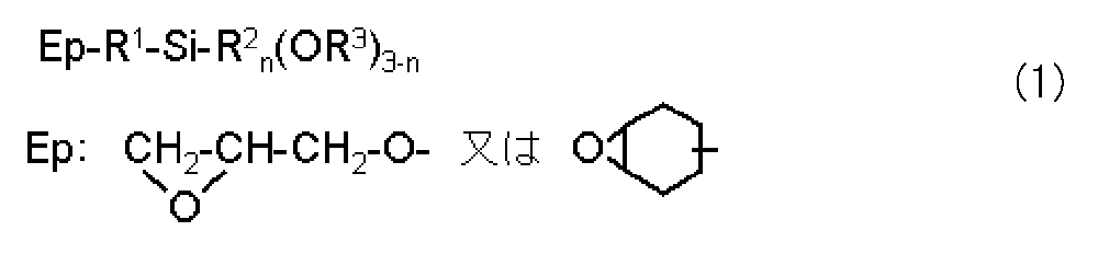
- a semiconductor element partially or wholly covered with polyimide is formed from an epoxy resin (A), a phenol resin (B), a curing accelerator (C), an inorganic filler (D), and a general formula ( 1):
- R 1 , R 2 and R 3 are hydrocarbon groups having 1 to 4 carbon atoms, which may be the same or different, and n is an integer of 0 to 2.
- the semiconductor device obtained by sealing with the epoxy resin composition for semiconductor sealing containing the silane coupling agent (E) represented by these and / or its hydrolysis-condensation product is provided.
- the silane coupling agent (E) and / or a hydrolysis condensate thereof is represented by the following formula (2): Or a hydrolysis-condensation product thereof.
- the proportion of the silane coupling agent (E) and / or the hydrolysis condensate thereof is 0.01 to 1.0 mass of the entire epoxy composition for semiconductor encapsulation. %.
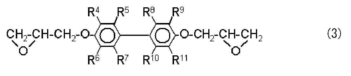
- the epoxy resin (A) is represented by the general formula (3): (In the general formula (3), R 4 to R 11 are each selected from a hydrogen atom and an alkyl group having 1 to 4 carbon atoms, and may be the same or different from each other) The epoxy resin represented by these is included.
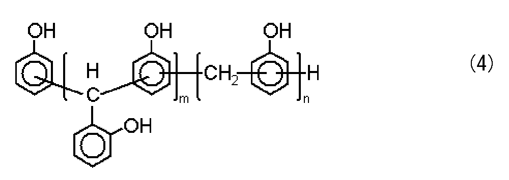
- the phenol resin (B) is represented by the general formula (4): (In the general formula (4), m is an integer of 1 to 5, and n is an integer of 0 to 5) The phenol resin represented by these is included.
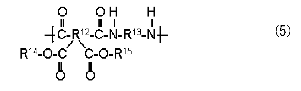
- the polyimide is represented by the general formula (5): (In general formula (5), R 12 is an organic group having at least 2 carbon atoms, R 13 is an organic group having at least 2 carbon atoms, and R 14 and R 15 are at least one An organic group having a heavy bond, which may be the same or different from each other) It is the polyimide obtained by dealcoholizing the polyimide precursor represented by these.
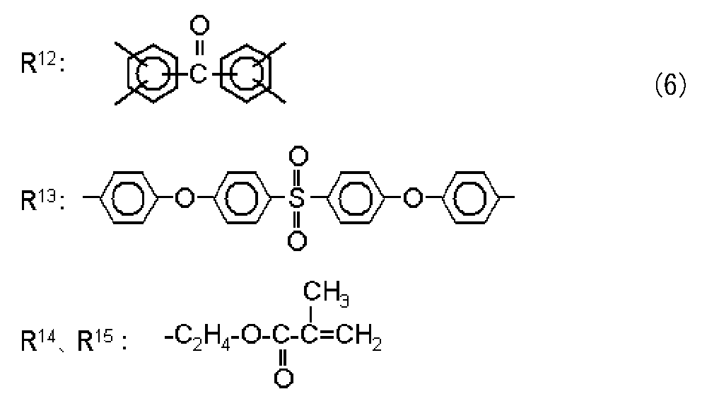
- R 12 , R 13 , R 14 , and R 15 of the polyimide precursor represented by the general formula (5) are represented by the following formula (6): It is group represented by these.
- the semiconductor device is an area mounting type semiconductor device, and the semiconductor element is mounted on one surface of the substrate of the semiconductor element, and only the surface of the substrate on which the semiconductor element is mounted is provided.
- a semiconductor device encapsulated with the above epoxy resin composition for encapsulating a semiconductor is provided.
- the semiconductor device is a board-on-chip semiconductor device, the semiconductor device is mounted on one side of a substrate having an opening, and the semiconductor element of the substrate is mounted.
- a semiconductor device is provided in which the surface and the opening are sealed with the semiconductor sealing epoxy resin composition.
- the present invention it is possible to obtain a semiconductor device having high adhesion between the polyimide film covering the surface of the semiconductor element and the sealing resin and having excellent solder resistance.
- the semiconductor device of the present invention comprises a semiconductor element partially or entirely covered with polyimide, an epoxy resin (A), a phenol resin (B), a curing accelerator (C), an inorganic filler (D), and general Sealed with an epoxy resin composition for semiconductor sealing containing a silane coupling agent (E) represented by formula (1) and / or a compound (hydrolysis condensate) obtained by hydrolyzing and condensing the silane coupling agent (E). It is characterized by being obtained.
- a silane coupling agent (E) represented by formula (1) and / or a compound (hydrolysis condensate) obtained by hydrolyzing and condensing the silane coupling agent (E).
- polyimide and its precursor which are one component of the semiconductor device in the present invention, will be described in detail.
- a polyimide is obtained by dealcoholizing or dehydrating the precursor.
- polyimide is classified into photosensitive polyimide and non-photosensitive polyimide, and photosensitive polyimide includes ester bond type polyimide and ion bond type polyimide.
- the polyimide used for the semiconductor device of this invention is not specifically limited,
- the polyimide obtained by dealcoholizing the photosensitive resin composition which has a polyimide precursor as a main component can be used.
- the polyimide precursor represented by General formula (5) can be used.
- R 12 is an organic group having at least 2 carbon atoms
- R 13 is an organic group having at least 2 carbon atoms
- R 14 and R 15 are at least one An organic group having a heavy bond, which may be the same or different.
- R 12 in the general formula (5) is an organic group having at least 2 carbon atoms.
- R 12 is introduced from a compound having an organic group.
- R 12 is a group containing an aromatic ring or an aromatic heterocyclic ring, the resulting polyimide has heat resistance.
- R 12 include 3,3 ′, 4,4′-benzophenone tetracarboxylic acid residue, pyromellitic acid residue, 4,4′-oxydiphthalic acid residue, and the like. It is not limited to. Of these, 3,3 ′, 4,4′-benzophenone tetracarboxylic acid residue is preferred from the viewpoint of heat resistance of polyimide. In using these, one kind or a mixture of two kinds or more may be used.
- R 13 is an organic group having at least 2 carbon atoms.
- R 13 is introduced from a compound having an organic group.
- R 13 is preferably a group containing an aromatic ring or an aromatic heterocyclic ring from the viewpoint of the heat resistance of the resulting polyimide.
- Preferred specific examples of R 13 include bis [4- (4-aminophenoxy) phenyl] sulfone residue, bis [4- (3-aminophenoxy) phenyl] sulfone residue, 4,4′-diaminodiphenyl.
- R 14 and R 15 are each independently an organic group having at least one double bond, preferably a photosensitive group having 1 to 3 acryl (methacryl) groups. is there.
- Examples of compounds for introducing R 14 and R 15 include 2-hydroxyethyl methacrylate, 2-hydroxyethyl acrylate, glycidyl methacrylate, glycidyl acrylate, 2-hydroxypropyl methacrylate, 2-hydroxypropyl acrylate, pentaerythritol tris.
- a well-known technique can be used about the manufacturing method of a polyimide precursor (5), and it does not specifically limit.
- An example of a method for producing polyimide will be described.
- a compound having an alcohol group for introducing the photosensitive groups R 14 and R 15 is dissolved in a solvent, and an excess acid anhydride or a derivative thereof is reacted therewith. Then, it can synthesize
- the photosensitive polyimide composition containing the above polyimide is a sensitizer, initiator, preservability improver, adhesion aid, inhibitor, leveling agent, and other various fillers to improve lithography properties such as sensitivity and resolution. May be added.
- a well-known technique can be used for the method of coating the semiconductor element in the present invention with the photosensitive polyimide composition, and is not particularly limited.
- An example of the coating method will be described.
- the photosensitive polyimide composition is applied to a suitable support, such as a silicon wafer, ceramic, aluminum substrate or the like.
- a coating method spin coating using a spinner, spray coating using a spray coater, dipping, printing, roll coating, or the like can be used.
- the coating film thickness can be adjusted by the coating means, the solid content concentration of the composition, and the viscosity, but is usually in the range of 1 to 30 ⁇ m.
- the coating film is dried by pre-baking at a low temperature of 60 to 80 ° C., and actinic radiation is irradiated to a desired pattern shape.
- actinic radiation X-rays, electron beams, ultraviolet rays, visible rays and the like can be used, but those having a wavelength of 200 to 500 nm are preferable.
- a relief pattern is obtained by dissolving and removing the unirradiated portion with a developer.
- N-methyl-2-pyrrolidone, N, N-dimethylacetamide, N, N-dimethylformamide, etc., methanol, xylene, isopropyl alcohol, water, an aqueous alkaline solution, or the like can be used alone or in combination.
- spraying, paddle, dipping, ultrasonic waves, etc. can be used.
- the relief pattern formed by development is rinsed with a rinse solution.
- rinsing liquid methanol, xylene, ethanol, isopropyl alcohol, butyl acetate, water and the like can be used.
- heat treatment is performed to form an imide ring, thereby obtaining a final pattern rich in heat resistance.
- a preferable heat treatment temperature is 70 to 450 ° C., more preferably 150 to 400 ° C.
- the semiconductor element in which part or all of the semiconductor element is covered with polyimide is, for example, the polyimide on the electrode pad is removed so that the electrode pad is exposed for electrical connection from the electrode pad to the outside. It means to include.
- the epoxy resin composition for semiconductor encapsulation of the present invention is represented by the epoxy resin (A), the phenol resin (B), the curing accelerator (C), the inorganic filler (D), and the general formula (1). It contains a silane coupling agent (E) and / or a hydrolysis condensate thereof.
- epoxy resin (A) used with the epoxy resin composition for semiconductor sealing of this invention For example, biphenyl type epoxy resin, bisphenol A type epoxy resin, bisphenol F type epoxy resin, etc. Crystalline epoxy resin; Novolak type epoxy resin such as phenol novolac type epoxy resin and cresol novolak type epoxy resin; Multifunctional type epoxy resin such as triphenolmethane type epoxy resin and alkyl-modified triphenolmethane type epoxy resin; having phenylene skeleton Aralkyl type epoxy resins such as phenol aralkyl type epoxy resins, phenol aralkyl type epoxy resins having a biphenylene skeleton, naphthol aralkyl type epoxy resins having a phenylene skeleton; Type epoxy resin, epoxy resin having a naphthalene skeleton such as dihydroxynaphthalene type epoxy resin; triazine nucleus-containing epoxy resin such as triglycidyl isocyanurate and monoallyl diglycidy
- an epoxy as the resin (A) is preferably a biphenyl type epoxy resin represented by the general formula (3), R 4, R 6, R 9, R 11 is a methyl group of the general formula (3), R 5
- An epoxy resin in which R 7 , R 8 and R 10 are hydrogen atoms is more preferable. Since such an epoxy resin has a low viscosity, the filler can be highly filled, and the water absorption of the cured epoxy resin can be reduced. Furthermore, since they have a bifunctional and highly heat-resistant skeleton structure, the reliability of solder resistance is further improved.
- R 4 to R 11 are each selected from a hydrogen atom and an alkyl group having 1 to 4 carbon atoms, and may be the same or different from each other).
- the phenol resin (B) used in the epoxy resin composition for semiconductor encapsulation of the present invention is not particularly limited.
- a novolak type resin such as a phenol novolak resin or a cresol novolak resin
- a triphenol type methane resin Polyfunctional phenol resins such as triphenolmethane and phenol novolac copolymer resins
- aralkyl resins such as phenol aralkyl phenol resins (having a phenylene skeleton and biphenylene skeleton) and naphthol aralkyl resins
- terpene-modified phenol resins examples thereof include modified phenolic resins such as dicyclopentadiene-modified phenolic resins, and these may be used alone or in combination of two or more.
- the polyfunctional type phenol resin represented by General formula (4) is preferable.
- the warpage characteristic in the area mounting type semiconductor device is improved, and the solder resistance reliability is further improved.
- m is an integer of 1 to 5
- n is an integer of 0 to 5).
- the equivalent ratio (EP / OH) of the number of epoxy groups (EP) of all epoxy resins and the number of phenolic hydroxyl groups (OH) of all phenol resins used in the epoxy resin composition for semiconductor encapsulation of the present invention is preferably 0.5.
- the above is 2 or less, particularly preferably 0.7 or more and 1.5 or less.
- the equivalent ratio is in the above range, it is possible to suppress a decrease in moisture resistance, curability and the like.
- Examples of the curing accelerator (C) used in the epoxy resin composition for semiconductor encapsulation of the present invention include diazabicycloalkenes such as 1,8-diazabicyclo (5,4,0) undecene-7 and derivatives thereof; Organic phosphines such as phenylphosphine and methyldiphenylphosphine; tetraphenylphosphonium / tetraphenylborate, tetraphenylphosphonium / tetrabenzoic acid borate, tetraphenylphosphonium / tetranaphthoic acid borate, tetraphenylphosphonium / tetranaphthoyloxyborate, tetra Examples include tetra-substituted phosphonium and tetra-substituted borates such as phenylphosphonium and tetranaphthyloxyborate; adducts of pho
- the inorganic filler (D) used in the epoxy resin composition for semiconductor encapsulation of the present invention those generally used for epoxy resin compositions for semiconductor encapsulation can be used.
- fused spherical silica, fused crushed silica, crystalline silica, talc, alumina, titanium white, silicon nitride and the like can be mentioned, and fused spherical silica is most preferably used.
- These inorganic fillers may be used alone or in combination of two or more. These may be surface-treated with a coupling agent.
- the shape of the inorganic filler (D) is preferably as spherical as possible and the particle size distribution is broad in order to improve fluidity.
- the content of the inorganic filler (D) used in the present invention is preferably 83% by mass or more and 95% by mass or less, more preferably 87% by mass or more and 93% by mass or less in the total epoxy resin composition. It is.
- a resin composition having low hygroscopicity, low thermal expansion, sufficient solder resistance and good warpage characteristics can be obtained, and the fluidity is lowered and molded. Occurrence of filling defects at the time, and inconveniences such as deformation of the gold wire in the semiconductor device due to high viscosity can be suppressed.
- the epoxy resin composition for semiconductor encapsulation of this invention contains the silane coupling agent (E) represented by General formula (1) and / or its hydrolysis condensate.
- E silane coupling agent represented by General formula (1)
- R 1 , R 2 and R 3 are hydrocarbon groups having 1 to 4 carbon atoms, which may be the same or different, and n is an integer of 0 to 2. ).
- silane coupling agent examples include ⁇ -glycidoxypropyltrimethoxysilane, ⁇ -glycidoxypropylmethyldimethoxysilane, ⁇ -glycidoxypropyldimethylmethoxysilane, ⁇ -glycidoxypropyltrimethoxysilane.
- the hydrolysis-condensation product which is a compound obtained by hydrolyzing and polycondensing the silane coupling agent represented by following formula (2) is preferable.
- a resin having a poor solder resistance for example, an epoxy resin composition for semiconductor encapsulation containing a combination of a biphenyl type epoxy resin and a phenol novolac resin is used, the polyimide film and As the adhesion is improved, the solder resistance can be improved.
- an acidic or basic catalyst may be used to accelerate the hydrolysis reaction.
- acetic acid such as acetic acid, aluminum chloride, Lewis acid such as iron chloride, triphenylphosphine, basic catalyst such as 1,8-diazabicyclo (5,4,0) undecene-7 (DBU) Can be used.
- the ratio of the silane coupling agent (E) and / or the hydrolysis condensate thereof is preferably 0.01 to 1.0% by mass, more preferably 0.1 to 0.5% by mass, based on the entire composition.
- the content of the silane coupling agent (E) and / or its hydrolysis condensate is in the above range, the adhesion with the polyimide film is improved, and a resin composition capable of imparting good solder resistance is obtained. In addition, it is possible to suppress the occurrence of inconvenience such as a decrease in mechanical strength.
- the silane coupling agent (E) and / or the hydrolysis condensate thereof can be used in combination with other coupling agents as long as they do not impair the effect.
- silane coupling agents such as mercaptosilane, aminosilane, alkylsilane, ureidosilane, vinylsilane, titanate coupling agent, aluminum coupling agent, aluminum / zirconium coupling Coupling agents such as agents are listed.
- the epoxy resin composition for semiconductor encapsulation of the present invention includes components (A) to (E) described above, natural wax such as carnauba wax, synthetic wax such as polyethylene wax, stearic acid and stearic acid as necessary. Higher fatty acids such as zinc acid and metal salts thereof, or mold release agents such as paraffin; Colorants such as carbon black and bengara; Brominated epoxy resin, antimony trioxide, aluminum hydroxide, magnesium hydroxide, zinc borate, molybdic acid Flame retardants such as zinc and phosphazene; inorganic ion exchangers such as bismuth oxide hydrate; various additives such as antioxidants can be appropriately blended.
- the components (A) to (F), other additives, and the like are mixed at room temperature using a mixer or the like, if necessary, and then rolled, Dispersity, flow characteristics, etc. can be adjusted by heating and kneading with a kneader such as a kneader or an extruder, and pulverizing after cooling.
- a kneader such as a kneader or an extruder
- the semiconductor device of the present invention is obtained by encapsulating an electronic component such as a semiconductor element with the above-described epoxy resin composition for encapsulating a semiconductor and curing and molding by a conventional molding method such as a transfer mold, a compression mold, or an injection mold. be able to. As other semiconductor device manufacturing methods, known methods can be used. In addition, a semiconductor device can be obtained through a process of separating and molding a plurality of semiconductor elements in a lump and then separating them.
- Examples of the semiconductor element to be sealed include, but are not limited to, an integrated circuit, a large-scale integrated circuit, a transistor, a thyristor, a diode, and a solid-state imaging element.
- DIP dual in-line package
- PLCC chip carrier with plastic lead
- QFP quad flat package
- LQFP low profile quad flat package
- SOP Small Outline Package
- SOJ Small Outline J Lead Package
- TSOP Thin Small Outline Package
- TQFP Tape Carrier Package
- BGA ball grid array
- CSP chip size package
- BOC board on chip
- a MAP type ball grid array BGA
- a MAP type chip size package CSP
- MAP type quad flat non-lead QFN
- a semiconductor device in which a semiconductor element is encapsulated by a molding method such as transfer molding of a resin composition for encapsulating a semiconductor is used as it is or at a temperature of about 80 ° C. to 200 ° C. for about 10 minutes to 10 hours. After completely curing the resin composition, it is mounted on an electronic device or the like.
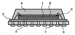
- FIG. 1 is a diagram showing a cross-sectional structure of an example of a single-side sealed semiconductor device using a semiconductor sealing resin composition according to the present invention.
- a laminated solder resist 5 is provided on the surface of the substrate 6, and the semiconductor element 1 covered with the polyimide film 8 is fixed on the solder resist 5 via the die bond material cured body 2.
- the semiconductor device of FIG. 1 is designed to connect the electrode pad of the semiconductor element 1 and the electrode pad on the substrate 6 by the bonding wire 3.
- the blending ratio is part by mass.
- Example 1 The following materials were mixed with a mixer, kneaded using two rolls with surface temperatures of 90 ° C. and 45 ° C., cooled and pulverized to prepare an epoxy resin composition.
- the obtained epoxy resin composition was evaluated by the following methods. The results are shown in Table 1.
- Epoxy resin 1 biphenyl type epoxy resin represented by the general formula (3) (manufactured by Japan Epoxy Resin Co., Ltd., YX4000K, melting point 105 ° C., epoxy equivalent 185, R 4 , R 6 , R 9 in the general formula (3), in R 11 is a methyl group, R 5, R 7, R 8, R 10 is mainly composed of component a hydrogen atom): 7.1 parts by weight
- Phenol resin 1 polyfunctional phenol resin represented by the general formula (4) (manufactured by Air Water Co., HE910-20, softening point 88 ° C., hydroxyl group equivalent 101): 3.9 parts by mass
- Curing accelerator represented by the following formula (7): 0.3 part by mass
- Silane coupling agent 1 Hydrolysis and shrinkage of silane coupling agent represented by the following formula (2) (manufactured by Nihon Unicar Co., Ltd., AZ-6137) Silane coupling agent obtained by polymerization: 0.2 parts by mass Mold release agent: glycerin trimontanic acid ester (manufactured by Clariant Japan Co., Ltd., Ricolbu (registered trademark) WE4): 0.2 part by mass Carbon black (manufactured by Mitsubishi Chemical Industries, Ltd., MA600): 0.3 part by mass
- Evaluation method Spiral flow Using a low-pressure transfer molding machine (KTS-15, manufactured by Kotaki Seiki Co., Ltd.), a spiral flow measurement mold according to ANSI / ASTM D 3123-72, mold temperature 175 ° C., injection pressure The epoxy resin composition was injected under conditions of 6.9 MPa and a curing time of 120 seconds, and the flow length was measured. The unit is cm.
- KTS-15 low-pressure transfer molding machine
- Solder resistance 1 Using a low-pressure transfer molding machine (TOWA Co., Ltd., Y series), a mold temperature of 175 ° C., an injection pressure of 6.9 MPa, a curing time of 2 minutes, and a 352-pin BGA (substrate thickness 0.56 mm) (Bismaleimide / triazine resin / glass cloth substrate, package size 30 mm ⁇ 30 mm, thickness 1.17 mm) and post-cured at 175 ° C. for 4 hours to obtain a sample. Each of the 10 obtained packages was subjected to a moisture absorption treatment in an environment of 60 ° C.
- Solder resistance 2 Solder resistance 1 was performed in the same manner as solder resistance 1 except that the moisture absorption time for solder resistance 1 was 168 hours.
- solder resistances 1 and 2 the following surface of the semiconductor element was coated with the following polyimide film with a thickness of 5 ⁇ m.
- Semiconductor element Size 10 mm ⁇ 10 mm, thickness 0.35 mm.
- Polyimide film a dehydration condensate (polyimide precursor) of 2-hydroxyethyl methacrylate diester of 3,3 ′, 4,4′-benzophenonetetracarboxylic acid and bis [4- (4-aminophenoxy) phenyl] sulfone, Polyimide obtained by dealcoholization.
- Package warpage amount Ten samples each formed by the same method as in the evaluation of solder resistance, using a surface roughness shape measuring instrument (Surfcom 408A, manufactured by Tokyo Seimitsu Co., Ltd.) diagonally from the gate of the package. The displacement in the height direction was measured, and the value with the largest displacement difference was taken as the amount of warpage. The unit is ⁇ m.
- Epoxy resin 2 Orthocresol novolac type epoxy resin (DIC Corporation, N660, softening point 62 ° C., epoxy equivalent 210)
- Phenol resin 2 Phenol novolac resin (manufactured by Sumitomo Bakelite Co., Ltd., PR-HF-3, softening point 80 ° C., hydroxyl equivalent 104)
- Silane coupling agent 2 Silane coupling agent represented by the following formula (2) (manufactured by Nihon Unicar Co., Ltd., AZ-6137)
- Silane coupling agent 3 Silane coupling agent obtained by hydrolysis and condensation polymerization of a silane coupling agent represented by the following formula (8) (manufactured by Nihon Unicar Co., Ltd., A-187)
- Silane coupling agent 4 Silane coupling agent represented by the following formula (8) (Nihon Unicar Co., Ltd., A-187)
- Silane coupling agent 5 Silane coupling agent represented by the following formula (9) (Nihon Unicar Co., Ltd., A-186)
- Silane coupling agent 6 Silane coupling agent represented by formula (10) (manufactured by Shin-Etsu Chemical Co., Ltd., KBM573)
- the epoxy resin compositions of Examples 1 to 10 are epoxy resin (A), phenol resin (B), curing accelerator (C), inorganic filler (D), and silane represented by general formula (1).
- the types are as shown in Table 1.
- the epoxy resin 1 which is a biphenyl type epoxy resin represented by the general formula (3) is used as the epoxy resin (A), and the polyfunctional phenol resin represented by the general formula (4) is used as the phenol resin (B).
- the epoxy resin 1 is used as the epoxy resin (A)
- the phenol resin 1 is used as the phenol resin (B)
- the silane coupling agent (E) and / or its hydrolysis condensate is represented by the formula (2).
- Examples 1 to 3 and 8 using the silane coupling agent 1 which is a silane coupling agent obtained by hydrolysis and condensation polymerization of the silane coupling agent the blending amount of the silane coupling agent 1 and other Regardless of whether or not the silane coupling agent was used in combination, a very good result was obtained that peeling of the polyimide film and the sealing resin on the surface of the semiconductor element did not occur even under the condition of solder resistance 2.
Landscapes
- Chemical & Material Sciences (AREA)
- Organic Chemistry (AREA)
- Chemical Kinetics & Catalysis (AREA)
- Health & Medical Sciences (AREA)
- Medicinal Chemistry (AREA)
- Polymers & Plastics (AREA)
- Life Sciences & Earth Sciences (AREA)
- Engineering & Computer Science (AREA)
- Materials Engineering (AREA)
- Wood Science & Technology (AREA)
- Structures Or Materials For Encapsulating Or Coating Semiconductor Devices Or Solid State Devices (AREA)
- Epoxy Resins (AREA)
- Compositions Of Macromolecular Compounds (AREA)
Abstract
Description

で表されるシランカップリング剤(E)および/またはその加水分解縮合物を含む半導体封止用エポキシ樹脂組成物によって封止して得られる半導体装置が提供される。

で表されるエポキシ樹脂を含む。

で表されるフェノール樹脂を含む。

で表されるポリイミド前駆体を脱アルコールして得られるポリイミドである。



下記材料をミキサーで混合した後、表面温度が90℃と45℃の2本ロールを用いて混練し、冷却後粉砕してエポキシ樹脂組成物を調製した。得られたエポキシ樹脂組成物を以下の方法で評価した。結果を表1に示す。
エポキシ樹脂1:一般式(3)で表されるビフェニル型エポキシ樹脂(ジャパンエポキシレジン株式会社製、YX4000K、融点105℃、エポキシ当量185、一般式(3)のR4、R6、R9、R11がメチル基で、R5、R7、R8、R10が水素原子である成分を主成分とする):7.1質量部


シランカップリング剤1:下記式(2)で表されるシランカップリング剤(日本ユニカー株式会社製、AZ-6137)を加水分解し縮重合して得られたシランカップリング剤:0.2質量部

カーボンブラック(三菱化学工業株式会社製、MA600):0.3質量部
スパイラルフロー:低圧トランスファー成形機(コータキ精機株式会社製、KTS-15)を用いて、ANSI/ASTM D 3123-72に準じたスパイラルフロー測定用金型に、金型温度175℃、注入圧力6.9MPa、硬化時間120秒の条件でエポキシ樹脂組成物を注入し、流動長を測定した。単位はcm。
耐半田性2: 耐半田性1の吸湿処理時間を168時間とした以外は耐半田性1と同様に実施した。
半導体素子:サイズ10mm×10mm、厚さ0.35mm。
ポリイミド膜:3,3',4,4'-ベンゾフェノンテトラカルボン酸の2-ヒドロキシエチルメタクリレートジエステルとビス[4-(4-アミノフェノキシ)フェニル]スルホンとの脱水縮合体(ポリイミド前駆体)を、脱アルコールして得られたポリイミド。
表1の配合に従い、実施例1と同様にしてエポキシ樹脂組成物を調製し、同様に評価した。これらの評価結果を表1に示す。
エポキシ樹脂2:オルソクレゾールノボラック型エポキシ樹脂(DIC株式会社製、N660、軟化点62℃、エポキシ当量210)
フェノール樹脂2:フェノールノボラック樹脂(住友ベークライト株式会社製、PR-HF-3、軟化点80℃、水酸基当量104)

シランカップリング剤4:下記式(8)で表されるシランカップリング剤(日本ユニカー株式会社製、A-187)




Claims (9)
- ポリイミドにより一部または全部が被覆された半導体素子を、エポキシ樹脂(A)、フェノール樹脂(B)、硬化促進剤(C)、無機充填材(D)、ならびに、一般式(1):
(一般式(1)において、R1、R2、R3は炭素数1~4の炭化水素基であり、互いに同一であっても異なっていてもよい、nは0~2の整数である)
で表されるシランカップリング剤(E)および/またはその加水分解縮合物を含む半導体封止用エポキシ樹脂組成物によって封止して得られる半導体装置。 - 前記シランカップリング剤(E)および/またはその加水分解縮合物が下記式(2):
で表されるシランカップリング剤および/またはその加水分解縮合物である請求項1記載の半導体装置。
- 前記シランカップリング剤(E)および/またはその加水分解縮合物の割合が半導体封止用エポキシ組成物全体の0.01~1.0質量%である請求項1に記載の半導体装置。
- 前記エポキシ樹脂(A)が一般式(3):
(一般式(3)において、R4~R11は各々、水素原子および炭素数1~4のアルキル基から選ばれ、互いに同一であっても異なっていてもよい)
で表されるエポキシ樹脂を含む請求項1に記載の半導体装置。 - 前記フェノール樹脂(B)が一般式(4):
(一般式(4)において、mは1~5の整数であり、nは0~5の整数である)
で表されるフェノール樹脂を含む請求項1に記載の半導体装置。 - 前記ポリイミドが一般式(5):
(一般式(5)において、R12は少なくとも2個の炭素原子を有する有機基であり、R13は少なくとも2個の炭素原子を有する有機基であり、R14およびR15は少なくとも一つの二重結合を有する有機基であり、互いに同一であっても異なっていてもよい)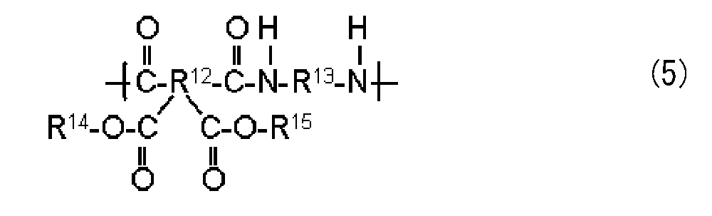
で表されるポリイミド前駆体を脱アルコールして得られるポリイミドである請求項1に記載の半導体装置。 - 前記一般式(5)で表されるポリイミド前駆体のR12、R13、R14、R15が下記式(6):
で表される基である請求項6に記載の半導体装置。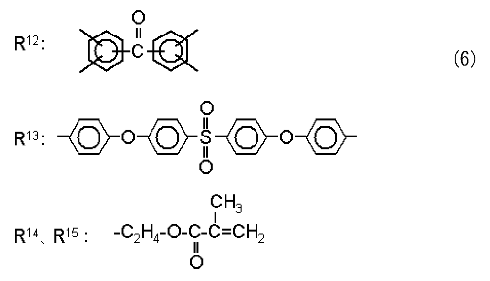
- 前記半導体素子が基板の片面に搭載され、前記基板の前記半導体素子が搭載された面のみが、前記半導体封止用エポキシ樹脂組成物で封止されている、エリア実装型半導体装置である請求項1に記載の半導体装置。
- 前記半導体素子が開口部を有する基板の片面に搭載され、前記基板の前記半導体素子が搭載された面および前記開口部が、前記半導体封止用エポキシ樹脂組成物で封止されている、ボード・オン・チップ型半導体装置である請求項1に記載の半導体装置。
Priority Applications (4)
| Application Number | Priority Date | Filing Date | Title |
|---|---|---|---|
| CN201080052423.8A CN102612743B (zh) | 2009-11-19 | 2010-11-11 | 半导体装置 |
| US13/510,734 US20120228784A1 (en) | 2009-11-19 | 2010-11-11 | Semiconductor device |
| JP2011541802A JP5761026B2 (ja) | 2009-11-19 | 2010-11-11 | 半導体装置 |
| KR1020177020756A KR20170088448A (ko) | 2009-11-19 | 2010-11-11 | 반도체 장치 |
Applications Claiming Priority (2)
| Application Number | Priority Date | Filing Date | Title |
|---|---|---|---|
| JP2009263702 | 2009-11-19 | ||
| JP2009-263702 | 2009-11-19 |
Publications (1)
| Publication Number | Publication Date |
|---|---|
| WO2011061906A1 true WO2011061906A1 (ja) | 2011-05-26 |
Family
ID=44059393
Family Applications (1)
| Application Number | Title | Priority Date | Filing Date |
|---|---|---|---|
| PCT/JP2010/006617 Ceased WO2011061906A1 (ja) | 2009-11-19 | 2010-11-11 | 半導体装置 |
Country Status (7)
| Country | Link |
|---|---|
| US (1) | US20120228784A1 (ja) |
| JP (1) | JP5761026B2 (ja) |
| KR (2) | KR20170088448A (ja) |
| CN (1) | CN102612743B (ja) |
| SG (1) | SG10201407493PA (ja) |
| TW (1) | TWI535776B (ja) |
| WO (1) | WO2011061906A1 (ja) |
Cited By (2)
| Publication number | Priority date | Publication date | Assignee | Title |
|---|---|---|---|---|
| JP2018053243A (ja) * | 2016-09-23 | 2018-04-05 | 住友ベークライト株式会社 | 熱硬化性樹脂組成物、樹脂封止基板、および電子装置 |
| JP2019151708A (ja) * | 2018-03-01 | 2019-09-12 | 株式会社日本触媒 | 樹脂組成物および光学フィルター |
Families Citing this family (1)
| Publication number | Priority date | Publication date | Assignee | Title |
|---|---|---|---|---|
| KR20160097429A (ko) * | 2015-02-06 | 2016-08-18 | 삼성디스플레이 주식회사 | 표시 장치 |
Citations (3)
| Publication number | Priority date | Publication date | Assignee | Title |
|---|---|---|---|---|
| JPH09176278A (ja) * | 1995-12-27 | 1997-07-08 | Sumitomo Bakelite Co Ltd | 半導体封止用エポキシ樹脂成形材料及びその製造方法 |
| JPH1112440A (ja) * | 1997-06-25 | 1999-01-19 | Sumitomo Bakelite Co Ltd | 半導体封止用エポキシ樹脂組成物 |
| JP2002080694A (ja) * | 2000-09-05 | 2002-03-19 | Sumitomo Bakelite Co Ltd | エポキシ樹脂組成物及び半導体装置 |
Family Cites Families (15)
| Publication number | Priority date | Publication date | Assignee | Title |
|---|---|---|---|---|
| TW378345B (en) * | 1997-01-22 | 2000-01-01 | Hitachi Ltd | Resin package type semiconductor device and manufacturing method thereof |
| JP2000183239A (ja) * | 1998-12-11 | 2000-06-30 | Toray Ind Inc | 半導体装置 |
| US6358629B1 (en) * | 1999-03-31 | 2002-03-19 | Mitsubishi Denki Kabushiki Kaisha | Epoxy resin composition and semiconductor device using the same |
| US6376100B1 (en) * | 1999-06-09 | 2002-04-23 | Shin Etsu-Chemical Co., Ltd. | Flip-chip type semiconductor device underfill material and flip-chip type semiconductor device |
| JP2002040654A (ja) * | 2000-07-31 | 2002-02-06 | Sumitomo Bakelite Co Ltd | ポジ型感光性樹脂組成物 |
| JP4250987B2 (ja) * | 2003-03-25 | 2009-04-08 | 住友ベークライト株式会社 | エポキシ樹脂組成物及び半導体装置 |
| SG110189A1 (en) * | 2003-09-26 | 2005-04-28 | Japan Epoxy Resins Co Ltd | Epoxy compound, preparation method thereof, and use thereof |
| JP4736406B2 (ja) * | 2004-11-18 | 2011-07-27 | 住友ベークライト株式会社 | エポキシ樹脂組成物及び半導体装置 |
| CN1808702A (zh) * | 2005-01-20 | 2006-07-26 | 矽品精密工业股份有限公司 | 半导体封装结构及其制法 |
| US7560821B2 (en) * | 2005-03-24 | 2009-07-14 | Sumitomo Bakelite Company, Ltd | Area mount type semiconductor device, and die bonding resin composition and encapsulating resin composition used for the same |
| JP5400267B2 (ja) * | 2005-12-13 | 2014-01-29 | 日立化成株式会社 | 封止用エポキシ樹脂組成物及び電子部品装置 |
| EP1911579A1 (en) * | 2006-10-04 | 2008-04-16 | Shin-Etsu Chemical Co., Ltd. | Epoxy resin composition for encapsulating semiconductor device and thin semicondutor device |
| JP2008163138A (ja) * | 2006-12-27 | 2008-07-17 | Sumitomo Bakelite Co Ltd | 半導体封止用エポキシ樹脂組成物及び半導体装置 |
| JP5183949B2 (ja) * | 2007-03-30 | 2013-04-17 | 日本電気株式会社 | 半導体装置の製造方法 |
| JP5133598B2 (ja) * | 2007-05-17 | 2013-01-30 | 日東電工株式会社 | 封止用熱硬化型接着シート |
-
2010
- 2010-11-11 US US13/510,734 patent/US20120228784A1/en not_active Abandoned
- 2010-11-11 KR KR1020177020756A patent/KR20170088448A/ko not_active Ceased
- 2010-11-11 CN CN201080052423.8A patent/CN102612743B/zh not_active Expired - Fee Related
- 2010-11-11 SG SG10201407493PA patent/SG10201407493PA/en unknown
- 2010-11-11 JP JP2011541802A patent/JP5761026B2/ja not_active Expired - Fee Related
- 2010-11-11 KR KR1020127015401A patent/KR20120104247A/ko not_active Ceased
- 2010-11-11 WO PCT/JP2010/006617 patent/WO2011061906A1/ja not_active Ceased
- 2010-11-18 TW TW099139678A patent/TWI535776B/zh not_active IP Right Cessation
Patent Citations (3)
| Publication number | Priority date | Publication date | Assignee | Title |
|---|---|---|---|---|
| JPH09176278A (ja) * | 1995-12-27 | 1997-07-08 | Sumitomo Bakelite Co Ltd | 半導体封止用エポキシ樹脂成形材料及びその製造方法 |
| JPH1112440A (ja) * | 1997-06-25 | 1999-01-19 | Sumitomo Bakelite Co Ltd | 半導体封止用エポキシ樹脂組成物 |
| JP2002080694A (ja) * | 2000-09-05 | 2002-03-19 | Sumitomo Bakelite Co Ltd | エポキシ樹脂組成物及び半導体装置 |
Cited By (4)
| Publication number | Priority date | Publication date | Assignee | Title |
|---|---|---|---|---|
| JP2018053243A (ja) * | 2016-09-23 | 2018-04-05 | 住友ベークライト株式会社 | 熱硬化性樹脂組成物、樹脂封止基板、および電子装置 |
| JP6996169B2 (ja) | 2016-09-23 | 2022-01-17 | 住友ベークライト株式会社 | 熱硬化性樹脂組成物、樹脂封止基板、および電子装置 |
| JP2019151708A (ja) * | 2018-03-01 | 2019-09-12 | 株式会社日本触媒 | 樹脂組成物および光学フィルター |
| JP7128633B2 (ja) | 2018-03-01 | 2022-08-31 | 株式会社日本触媒 | 樹脂組成物および光学フィルター |
Also Published As
| Publication number | Publication date |
|---|---|
| TWI535776B (zh) | 2016-06-01 |
| JP5761026B2 (ja) | 2015-08-12 |
| CN102612743B (zh) | 2016-08-10 |
| US20120228784A1 (en) | 2012-09-13 |
| CN102612743A (zh) | 2012-07-25 |
| KR20120104247A (ko) | 2012-09-20 |
| JPWO2011061906A1 (ja) | 2013-04-04 |
| SG10201407493PA (en) | 2014-12-30 |
| KR20170088448A (ko) | 2017-08-01 |
| TW201129626A (en) | 2011-09-01 |
Similar Documents
| Publication | Publication Date | Title |
|---|---|---|
| JP7126186B2 (ja) | 封止用樹脂組成物、その硬化物、及び半導体装置 | |
| JP5761026B2 (ja) | 半導体装置 | |
| JP2007002110A (ja) | 半導体封止用樹脂組成物および半導体装置 | |
| JP5332094B2 (ja) | 半導体封止用樹脂組成物及び半導体装置 | |
| JP4770024B2 (ja) | エポキシ樹脂組成物及び半導体装置 | |
| JP2002012742A (ja) | エポキシ樹脂組成物及び半導体装置 | |
| JP2004292514A (ja) | エポキシ樹脂組成物及び半導体装置 | |
| JP3537224B2 (ja) | エポキシ樹脂系組成物及び樹脂封止型半導体装置 | |
| JP3956717B2 (ja) | 封止用エポキシ樹脂組成物及び片面封止型半導体装置 | |
| JPH11130938A (ja) | エポキシ樹脂組成物及び半導体装置 | |
| JPH11100491A (ja) | エポキシ樹脂組成物及び半導体装置 | |
| JP4639427B2 (ja) | エポキシ樹脂組成物及び半導体装置 | |
| JP4645147B2 (ja) | エポキシ樹脂組成物及び半導体装置 | |
| TWI741405B (zh) | 封止方法、封止層、封止層形成用之混合液、封止層之製造方法及半導體裝置 | |
| JP4765159B2 (ja) | エポキシ樹脂組成物及び半導体装置 | |
| JPH1192629A (ja) | エポキシ樹脂組成物及び半導体装置 | |
| JP2002121356A (ja) | エポキシ樹脂組成物及び半導体装置 | |
| JP5055778B2 (ja) | エポキシ樹脂組成物、エポキシ樹脂成形材料及び半導体装置 | |
| JP2000031344A (ja) | ボールグリッドアレイ型半導体装置 | |
| JP4524837B2 (ja) | エポキシ樹脂組成物及び半導体装置 | |
| JP3932254B2 (ja) | エポキシ樹脂組成物及び半導体装置 | |
| JP2002322344A (ja) | エポキシ樹脂組成物及び半導体装置 | |
| JP4556324B2 (ja) | エリア実装型半導体封止用エポキシ樹脂組成物及びエリア実装型半導体装置。 | |
| JPH1192630A (ja) | エポキシ樹脂組成物及び半導体装置 | |
| JP2006143865A (ja) | エポキシ樹脂組成物及び半導体装置 |
Legal Events
| Date | Code | Title | Description |
|---|---|---|---|
| WWE | Wipo information: entry into national phase |
Ref document number: 201080052423.8 Country of ref document: CN |
|
| 121 | Ep: the epo has been informed by wipo that ep was designated in this application |
Ref document number: 10831305 Country of ref document: EP Kind code of ref document: A1 |
|
| WWE | Wipo information: entry into national phase |
Ref document number: 2011541802 Country of ref document: JP |
|
| WWE | Wipo information: entry into national phase |
Ref document number: 13510734 Country of ref document: US |
|
| WWE | Wipo information: entry into national phase |
Ref document number: 1201002307 Country of ref document: TH |
|
| NENP | Non-entry into the national phase |
Ref country code: DE |
|
| ENP | Entry into the national phase |
Ref document number: 20127015401 Country of ref document: KR Kind code of ref document: A |
|
| 122 | Ep: pct application non-entry in european phase |
Ref document number: 10831305 Country of ref document: EP Kind code of ref document: A1 |