WO2011058622A1 - ヒートシンク、ヒートシンクアセンブリ、半導体モジュール及び冷却装置付き半導体装置 - Google Patents
ヒートシンク、ヒートシンクアセンブリ、半導体モジュール及び冷却装置付き半導体装置 Download PDFInfo
- Publication number
- WO2011058622A1 WO2011058622A1 PCT/JP2009/069187 JP2009069187W WO2011058622A1 WO 2011058622 A1 WO2011058622 A1 WO 2011058622A1 JP 2009069187 W JP2009069187 W JP 2009069187W WO 2011058622 A1 WO2011058622 A1 WO 2011058622A1
- Authority
- WO
- WIPO (PCT)
- Prior art keywords
- heat
- heat sink
- semiconductor module
- semiconductor
- cooling device
- Prior art date
- Legal status (The legal status is an assumption and is not a legal conclusion. Google has not performed a legal analysis and makes no representation as to the accuracy of the status listed.)
- Ceased
Links
Images





Classifications
-
- H—ELECTRICITY
- H10—SEMICONDUCTOR DEVICES; ELECTRIC SOLID-STATE DEVICES NOT OTHERWISE PROVIDED FOR
- H10W—GENERIC PACKAGES, INTERCONNECTIONS, CONNECTORS OR OTHER CONSTRUCTIONAL DETAILS OF DEVICES COVERED BY CLASS H10
- H10W40/00—Arrangements for thermal protection or thermal control
- H10W40/40—Arrangements for thermal protection or thermal control involving heat exchange by flowing fluids
- H10W40/43—Arrangements for thermal protection or thermal control involving heat exchange by flowing fluids by flowing gases, e.g. forced air cooling
-
- F—MECHANICAL ENGINEERING; LIGHTING; HEATING; WEAPONS; BLASTING
- F28—HEAT EXCHANGE IN GENERAL
- F28F—DETAILS OF HEAT-EXCHANGE AND HEAT-TRANSFER APPARATUS, OF GENERAL APPLICATION
- F28F3/00—Plate-like or laminated elements; Assemblies of plate-like or laminated elements
- F28F3/02—Elements or assemblies thereof with means for increasing heat-transfer area, e.g. with fins, with recesses, with corrugations
- F28F3/04—Elements or assemblies thereof with means for increasing heat-transfer area, e.g. with fins, with recesses, with corrugations the means being integral with the element
- F28F3/048—Elements or assemblies thereof with means for increasing heat-transfer area, e.g. with fins, with recesses, with corrugations the means being integral with the element in the form of ribs integral with the element or local variations in thickness of the element, e.g. grooves, microchannels
-
- H—ELECTRICITY
- H05—ELECTRIC TECHNIQUES NOT OTHERWISE PROVIDED FOR
- H05K—PRINTED CIRCUITS; CASINGS OR CONSTRUCTIONAL DETAILS OF ELECTRIC APPARATUS; MANUFACTURE OF ASSEMBLAGES OF ELECTRICAL COMPONENTS
- H05K7/00—Constructional details common to different types of electric apparatus
- H05K7/20—Modifications to facilitate cooling, ventilating, or heating
- H05K7/2089—Modifications to facilitate cooling, ventilating, or heating for power electronics, e.g. for inverters for controlling motor
- H05K7/20909—Forced ventilation, e.g. on heat dissipaters coupled to components
-
- H—ELECTRICITY
- H10—SEMICONDUCTOR DEVICES; ELECTRIC SOLID-STATE DEVICES NOT OTHERWISE PROVIDED FOR
- H10W—GENERIC PACKAGES, INTERCONNECTIONS, CONNECTORS OR OTHER CONSTRUCTIONAL DETAILS OF DEVICES COVERED BY CLASS H10
- H10W40/00—Arrangements for thermal protection or thermal control
- H10W40/20—Arrangements for cooling
- H10W40/22—Arrangements for cooling characterised by their shape, e.g. having conical or cylindrical projections
-
- H—ELECTRICITY
- H10—SEMICONDUCTOR DEVICES; ELECTRIC SOLID-STATE DEVICES NOT OTHERWISE PROVIDED FOR
- H10W—GENERIC PACKAGES, INTERCONNECTIONS, CONNECTORS OR OTHER CONSTRUCTIONAL DETAILS OF DEVICES COVERED BY CLASS H10
- H10W40/00—Arrangements for thermal protection or thermal control
- H10W40/70—Fillings or auxiliary members in containers or in encapsulations for thermal protection or control
- H10W40/73—Fillings or auxiliary members in containers or in encapsulations for thermal protection or control for cooling by change of state
Definitions
- the present invention relates to a heat sink, a heat sink assembly, a semiconductor module, and a semiconductor device with a cooling device.
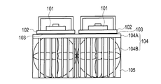
- a power semiconductor element cooling apparatus is bolted to a power semiconductor module 101 via an insulating material 102 and a thermal interface material 103 such as grease or heat conductive adhesive. It is the structure made to press-contact by doing. And the fan 105 is installed so that it may blow in the direction along the radiation fin 104B of the heat sink 104 for forced air cooling.
- Heat generated in the power semiconductor element during operation of the power conversion device is radiated from the power semiconductor module 101 to the surrounding environment (atmosphere) through the thermal interface material 103 at the contact boundary, through the base 104A of the heat sink 104 and the heat radiation fin 104B. Is done.
- the heat transfer rate (several tens of watts) of the heat sink 104 as the heat radiating portion with respect to the heat generation density (several hundred thousand W / m 2 ) of the power semiconductor element / m 2 K) is low, and in order to keep it within an acceptable temperature difference (several tens of degrees Celsius), it was necessary to expand the heat dissipation area to several hundred times the heat generation area.
- heat conduction resistance heat resistance due to solid heat conduction
- contact heat resistance heat resistance due to contact between solid and solid
- spreading heat resistance heat from the heat generating component spreading at an angle of 45 °
- Heat dissipation such as heat resistance transmitted to the heat sink 104
- fin efficiency correctedion that the temperature of the entire heat dissipation fin 104B is not uniform
- heat sink efficiency correctedion that the inlet and outlet temperatures are not uniform
- An obstructing factor occurs. For this reason, the volume of the heat sink 104 is much larger than the volume of the power semiconductor module 101.
- a power conversion device including the large IGBT module and the cooling device shown in FIG. 1 will be described. If the heat loss of the power semiconductor element is 2000 W and the allowable junction temperature is 125 ° C (ambient temperature 40 ° C), the large caulking heat sink 104 (W330mm ⁇ L300mm ⁇ H110mm) with the forced air cooling fan 105 is applied. Is one reasonable solution. At this time, since the heat resistance of the heat sink 104 is 0.028 K / W and the volume is 10890 cm 3 , the volume heat resistance is 305 cm 3 K / W (heat sink performance index).
- Non-Patent Document 1 This heat sink is also widely used as a cooling device for electric vehicles (Patent Document 1).
- Another means is a cooler that forcibly circulates refrigerant with a water-cooled pump or the like to transport heat.
- a microchannel is formed in the immediate vicinity of the heat generating component to reduce the heat conduction resistance, increase the heat radiation area and reduce the heat transfer resistance to the refrigerant, increase the heat flow rate that can be cooled, and Some have made cooling possible (Patent Documents 2 to 5).
- Patent Documents 6 and 7 there are some which use a collision jet to reduce heat transfer resistance and obtain the same effect.
- the heat receiving block can be reduced in size, but a separate gas-liquid heat exchanger is required for heat dissipation to the surrounding environment (atmosphere). .
- peripheral components drive pump and tube
- the volume of the water-cooled cooling device is equal to or greater than that of the heat pipe type or boiling cooling type cooling device.
- the conventional power semiconductor element cooling devices described in Non-Patent Document 1 and Patent Documents 1 to 7 described above require a heat transport mechanism by circulating refrigerant. For this reason, the cost of the whole heat sink including the heat receiving block, the heat transport mechanism, and the heat radiating fins has increased. Further, in these conventional power semiconductor element cooling devices, the heat receiving block and the heat radiating fins can be separated, and the degree of freedom in layout is high. However, the volume of the entire cooling device including the heat receiving block, the heat transport mechanism, and the heat radiating fin is about 1/2 to 1/3 and is not so small. Furthermore, there is a problem that countermeasures are required because the problem of freezing of the refrigerant and liquid leakage may occur.
- the present invention has been made to solve the above-described problems of the prior art, and can be used for a heat-generating semiconductor element to keep the temperature low, and to reduce the volume of the cooling means.
- An object of the present invention is to provide a heat sink that can be manufactured at low cost and can maintain high reliability, and a heat sink assembly using the heat sink, a semiconductor module, and a semiconductor device with a cooling device.
- a first technical feature of the present invention is a heat sink for use with a forced air cooling fan, and a large number of bases arranged in parallel at a narrow pitch of submillimeter order installed on one side of the base.
- Each of the plurality of heat radiation fins is a heat sink having a thickness of sub millimeter order, a length in the width direction of 60 mm or less, and a height of 40 mm or less. The length in the direction may be 10-60 mm, and the height may be 10-40 mm).
- a second technical feature of the present invention is a heat sink comprising at least two heat sinks according to the first technical feature of the present invention, and a heat transport device that thermally connects the at least two heat sinks. It is an assembly.
- a third technical feature of the present invention includes a heat sink according to the first technical feature of the present invention, a heat receiving block disposed in a thermally conductive state on the other surface of the base, and the heat receiving block.
- a semiconductor module comprising: an installed semiconductor element.
- a fourth technical feature of the present invention is a heat sink assembly according to the second technical feature of the present invention and capable of conducting heat on the other surface of the base with respect to at least one heat sink of the heat sink assembly. It is a semiconductor module provided with the heat receiving block arrange
- a semiconductor module according to the third or fourth technical feature of the present invention, a housing for housing the semiconductor module, and the semiconductor module attached to the housing.
- a cooling device-equipped semiconductor device including a fan that blows outside air to a large number of radiating fins.
- the temperature of the heat sink is used together with a forced air cooling fan as a cooling device for forcibly cooling the heat-generating semiconductor element.
- the volume of the cooling device can be reduced, and the reliability can be kept high by reducing the cost.
- the heat sink or the heat sink assembly is small, inexpensive, and highly reliable. Is used as a cooling means, so that it can be miniaturized as a semiconductor module provided with a cooling device and also as a semiconductor device.
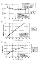
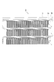
- FIG. 1 It is a perspective view of the cooling device of the conventional forced air cooling type power semiconductor element. It is sectional drawing of the cooling device of the conventional forced air cooling type power semiconductor element. It is a perspective view of the heat sink of Example 1 of this invention. It is a heat sink of Example 1 of this invention, Comprising: (a) is a front view, (b) is a side view. It is an enlarged view of the C section in FIG. It is a graph which shows the characteristic regarding the length of the heat sink which concerns on Example 1 of this invention, Comprising: (a) is the characteristic of thermal resistance, (b) is the characteristic of volume thermal resistance, (c) is the characteristic of optimal radiating fin shape. Indicates.
- the shape of the heat radiating fin that provides the best heat radiating capacity can be obtained by the following equation.
- H ar [Pa] is a fin hydraulic head and is given by the following equation.
- the heat sink length L is not required to be longer than a certain length when the heat dissipating fin shape having the best heat dissipating capability is taken.
- the conventional forced air-cooled heat sink for power semiconductor devices has a heat sink length of 200 mm to 300 mm, but the same heat dissipation capability can be realized with a heat sink length of 20 mm to 30 mm. I understand. Such a heat sink is advantageous in both miniaturization and cost reduction.
- the shape of the heat sink 1 includes a width W, a height H, and a length L corresponding to the outer shape of the heat sink 1, a thickness Tb of the cooling surface base 1A, a thickness Tf of the radiating fin 1B, and a gap Gf. And height Hf.
- the width W of the heat sink 1 is the length in the direction in which the radiating fins 1B are arranged.
- the length L of the heat sink 1 is the direction along the wind flow of the fan, and is equal to the width of the radiating fin 1B.
- each of the radiating fins 1B has a thickness of submillimeter order, and a large number of radiating fins 1B are arranged in parallel at a narrow pitch of submillimeter order. And the following three effects are acquired by making length L and height H of the heat sink 1 small.
- the first is that a large number of heat dissipating fins 1B having a thickness of submillimeter order are arranged in parallel at a narrow pitch, so that although the heat loss of the heat sink 1 increases, the total heat dissipating fin area increases. An effect equivalent to the increase in the length L is obtained. Therefore, the heat sink 1 of the first embodiment can be significantly shortened in length L and can be reduced in size as compared with the conventional heat sink.
- the utilization rate of the boundary run-up section increases because the length L of the heat sink 1 is shortened. For this reason, the heat sink 1 of Example 1 can obtain the heat dissipation capability superior to the conventional heat sink.
- a high-density heat radiation fin heat sink (W330mm ⁇ L15mm ⁇ H15mm ⁇ 3P) can be used to achieve the same performance as the conventional power semiconductor module cooling device shown in FIGS. It is.
- the heat resistance of the heat sink 1 is 0.028 K / W and the volume is 223 cm 3 , the volume heat resistance is 6.2 cm 3 K / W. Therefore, the heat sink according to the first embodiment can be reduced in size by about 1/50 compared with the conventional heat sink shown in FIGS.
- each of the radiating fins 1B has a thickness on the order of submillimeters, and the radiating fins 1B are formed with a narrow pitch, and the length L and the height H of the heat sink 1 are reduced. .
- the volume of the heat sink 1 can be significantly reduced, and since there is no heat transport mechanism by circulating refrigerant, an inexpensive and highly reliable semiconductor cooling device can be configured.
- each of the radiating fins 1B has not been possible to make it inexpensive to configure each of the radiating fins 1B to have a thickness of sub-millimeter order and to arrange a large number of radiating fins 1B in parallel at a narrow pitch.
- a technology such as precision machining press.
- the material cost of the conventional large caulking heat sink and the mass production cost of the high-density heat radiation fin heat sink according to the first embodiment are substantially equal.
- a high-density heat radiation fin heat sink having an equivalent thermal resistance can be provided at an equivalent cost and a size of several tenths. Accordingly, when the material cost increases in the future, the high-density heat radiation fin heat sink according to the first embodiment is more advantageous in terms of cost.
- Example 1 assumes the utilization to the cooling device of power semiconductor elements like IGBT and MOSFET, any of exothermic semiconductor elements, such as CPU and resistance, are assumed. Applicable.
- the heat radiation fin 1B has a thickness of a submillimeter order and a narrow pitch, there is anxiety about the strength and dirt of the heat radiation fin. Therefore, in such an environment, it is desirable to provide an air filter to prevent fouling.
- the fan 105 is a suction fan, an air filter may be provided at the suction port. If the fan 105 is an exhaust fan, an air filter may be provided at the suction port on the side opposite to the fan installation side of the housing that houses the cooling device.
- a heat sink assembly 5 according to Embodiment 2 of the present invention will be described with reference to FIG.
- a plurality of high-density heat radiation fin heat sinks 1 according to the first embodiment are connected in the height direction by heat transport devices 2 such as heat pipes and heat lanes, and a heat receiving block is provided on the heat receiving surface. 3 is installed.
- the heat receiving surface refers to the surface of the both sides of the base 1A where the large number of heat dissipating fins 1B are not disposed.
- the heat sink assembly 5 according to the second embodiment can be used as a forced air-cooled semiconductor element cooling device and a forced air-cooled semiconductor module cooling device.
- a semiconductor device 8 with a cooling device according to a third embodiment of the present invention will be described with reference to FIG.
- the heat receiving block 3 is arranged on the heat receiving surface of the base 1A of the high-density heat radiation fin heat sink 1 according to the first embodiment, and the power semiconductor element 6 is fixed on the heat receiving block 3.
- the power semiconductor module 9 is configured.
- the entire power semiconductor module 9 is built in the housing 7. And it is the structure which attached the fan 105 for air cooling to the housing
- the power semiconductor element 6 and the heat sink 1 are electrically connected, and the heat sink 1 is used as a part of the electrode terminal.
- a semiconductor device 10 with a cooling device according to a fourth embodiment of the present invention will be described with reference to FIG.
- the semiconductor device with a cooling device 10 according to the fourth embodiment includes a plurality of high-density heat radiation fin heat sinks 1 according to the first embodiment built in the housing 7 and receives heat from the heat receiving block 3 of each high-density heat radiation fin heat sink 1.
- a power semiconductor module 9 is configured by fixing the power semiconductor element 6 to the surface.
- the power semiconductor module 9 is built in the casing 7 in multiple stages, and an air cooling fan 105 is attached to the casing 7 in the same manner as shown in FIGS.
- each power semiconductor element 6 and the heat sink 1 are electrically connected, and the heat sink 1 is used as a part of the electrode terminal.
- the high density heat dissipating fin heat sinks 1 are arranged on both surfaces of the power semiconductor element 6 so that each heat sink 1 receives the heat of the power semiconductor element 6 by solder joint or pressure contact. It is also possible to do.
- the heat sink, heat sink assembly, semiconductor module and semiconductor device with a cooling device of the present invention can be used for a heat-generating semiconductor element to keep the temperature low, and the volume of the cooling means can be reduced. It is inexpensive and can maintain high reliability.
Landscapes
- Engineering & Computer Science (AREA)
- Physics & Mathematics (AREA)
- Thermal Sciences (AREA)
- Microelectronics & Electronic Packaging (AREA)
- Mechanical Engineering (AREA)
- General Engineering & Computer Science (AREA)
- Cooling Or The Like Of Electrical Apparatus (AREA)
- Cooling Or The Like Of Semiconductors Or Solid State Devices (AREA)
Abstract
Description
ヒートシンク長さL [m]、放熱フィン高さHfin [m]、ギャップg [m]の長方形ダクトの水力等価直径D [m]は、次の通りである。
D = 2 g Hfin /( g + Hfin )
レイノルズ数Reは、流体密度ρ [kg/m3]、流体粘度μ [Pa s]、放熱フィン平均流速Uar [m/s]から、次の通りである。
Re = ρ D Uar /μ
Re≒2300から乱流遷移が始まるが、狭いフィンピッチのヒートシンクは、ほとんどが層流流れである。無次元水力距離x+は、代表長さx(ヒートシンク長さL)から、次のようになる。
x+ = x / (Re D)
完全発達層流流れの摩擦係数fは、次のようになる。
f Re = (19.64 G + 4.7)
ここで、チャネルアスペクト比Gは、
〔数5〕
G = [(g / Hfin)2 + 1] / [(g + Hfin) + 1] 2
であり、発達中の層流流れの摩擦係数fappは、
〔数6〕
fapp Re = {[3.2 (x+)-0.57]2 + (f Re)2}1/2
である。層流流れが十分発達するまでの助走距離Xは、
〔数7〕
X / D = 0.0065 Re
であり、この助走距離区間内では圧力損失が余分に生じている。
〔数8〕
σ = g / p
であり、縮小係数Kcは、
〔数9〕
Kc = 0.8 - 0.4σ2
であり、拡大係数Keは、
〔数10〕
Ke = (1-σ)2
であり、ヒートシンクの圧力損失ΔPhs [Pa]は、
〔数11〕
ΔPhs = (Kc + 4fapp x+ + Ke) Har
である。
Har = ρ Uar 2 / 2
体積流量率V [m3/s]は、ヒートシンク幅W [m]から、
〔数13〕
V = WσHfinUar
である。
〔数14〕
P = V ΔP
である。
長方形ダクトの完全発達層流流れのヌセルト数Nuは、
〔数15〕
Nu = 8.31G - 0.02
であり、無次元サーマルチャネル長さx*は、プラントル数をPrとすると、
〔数16〕
x* = x / (Re D Pr)
である。
〔数17〕
Num = {[2.22 (x*)-0.33]3 + Nu3}1/3
であり、平均熱伝達係数hm [W/m2 K]は、空気の熱伝導率kf [W/m K]から、
〔数18〕
hm = Num kf / D
であり、ヒートシンクの対流熱抵抗θcon [K/W]は、ヒートシンク表面積Aw [m2]から、
〔数19〕
θcon = 1 / (hm Aw)
である。
〔数20〕
θcap = 1 / (V ρ cp)
であり、熱交換器で使われる概念の移動単位数NTUは、
〔数21〕
NTU = hm Aw / (V ρ cp)
である。
〔数22〕
ε = 1 - exp(-NUT)
である。
〔数23〕
η = tanh(b Hfin) / (b Hfin)
ここで、bは放熱フィンの熱伝導率ks [W/m K]から、
〔数24〕
b = [2hm/(ks t)]1/2
であり、ヒートシンクの熱抵抗θhs [K/W]は、
〔数25〕
θhs = θcap/(η ε)
である。
Claims (11)
- 強制空冷用ファンと共に使用するヒートシンクであって、
ベースと、
前記ベースの一方の面上に設置される、サブミリオーダーの狭ピッチで平行に配置された多数の放熱フィンと、
を備え、
前記多数の放熱フィンの各々は、厚さをサブミリオーダーとし、幅方向の長さを60 mm以下とし、高さを40 mm以下としたヒートシンク。 - 前記多数の放熱フィンの各々の厚さが0.1 ~ 0.6 mmであり、前記多数の放熱フィンを配置するサブミリオーダーの狭ピッチの値が0.4 ~ 1.3 mmである請求項1に記載のヒートシンク。
- 少なくとも2つの請求項1に記載のヒートシンクと、
前記少なくとも2つのヒートシンクの間を熱的に接続する熱輸送デバイスと、
を備えたヒートシンクアセンブリ。 - 請求項1に記載のヒートシンクと、
前記ベースの他方の面上に熱伝導可能な状態で配置された受熱ブロックと、
前記受熱ブロックに設置された半導体素子と、
を備えたことを特徴とする半導体モジュール。 - 請求項3に記載のヒートシンクアセンブリと、
前記ヒートシンクアセンブリの少なくとも1つの前記ヒートシンクに対して、前記ベースの他方の面上に熱伝導可能な状態で配置された受熱ブロックと、
前記受熱ブロックに設置された半導体素子と、
を備えた半導体モジュール。 - 前記半導体素子がパワー半導体素子である請求項4又は5に記載の半導体モジュール。
- 前記ヒートシンクが電極端子として用いられる請求項4又は5に記載の半導体モジュール。
- 請求項4に記載の半導体モジュールと、
前記半導体モジュールを収容する筐体と、
前記筐体に取り付けられ、前記半導体モジュールの前記多数の放熱フィンに対して外気を送風するファンと、
を備えた冷却装置付き半導体装置。 - 請求項5に記載の半導体モジュールと、
前記半導体モジュールを収容する筐体と、
前記筐体に取り付けられ、前記半導体モジュールの前記多数の放熱フィンに対して外気を送風するファンと、
を備えた冷却装置付き半導体装置。 - 前記筐体に外気を吸い込むための吸込口を形成し、前記吸気口にエアフィルタを設けたことを特徴とする請求項8又は9に記載の冷却装置付き半導体装置。
- 前記半導体素子が電力変換回路を構成している請求項8又は9に記載の冷却装置付き半導体装置。
Priority Applications (4)
| Application Number | Priority Date | Filing Date | Title |
|---|---|---|---|
| CN2009801624175A CN102598253A (zh) | 2009-11-11 | 2009-11-11 | 散热器、散热器组装体、半导体模块以及带冷却装置的半导体装置 |
| PCT/JP2009/069187 WO2011058622A1 (ja) | 2009-11-11 | 2009-11-11 | ヒートシンク、ヒートシンクアセンブリ、半導体モジュール及び冷却装置付き半導体装置 |
| DE112009005359T DE112009005359T5 (de) | 2009-11-11 | 2009-11-11 | Kühlkörper, Kühlkörperanordnung, Halbleitermodul und Halbleitereinrichtung mit einer Kühleinrichtung |
| US13/466,653 US8558373B2 (en) | 2009-11-11 | 2012-05-08 | Heatsink, heatsink assembly, semiconductor module, and semiconductor device with cooling device |
Applications Claiming Priority (1)
| Application Number | Priority Date | Filing Date | Title |
|---|---|---|---|
| PCT/JP2009/069187 WO2011058622A1 (ja) | 2009-11-11 | 2009-11-11 | ヒートシンク、ヒートシンクアセンブリ、半導体モジュール及び冷却装置付き半導体装置 |
Related Child Applications (1)
| Application Number | Title | Priority Date | Filing Date |
|---|---|---|---|
| US13/466,653 Continuation US8558373B2 (en) | 2009-11-11 | 2012-05-08 | Heatsink, heatsink assembly, semiconductor module, and semiconductor device with cooling device |
Publications (1)
| Publication Number | Publication Date |
|---|---|
| WO2011058622A1 true WO2011058622A1 (ja) | 2011-05-19 |
Family
ID=43991301
Family Applications (1)
| Application Number | Title | Priority Date | Filing Date |
|---|---|---|---|
| PCT/JP2009/069187 Ceased WO2011058622A1 (ja) | 2009-11-11 | 2009-11-11 | ヒートシンク、ヒートシンクアセンブリ、半導体モジュール及び冷却装置付き半導体装置 |
Country Status (4)
| Country | Link |
|---|---|
| US (1) | US8558373B2 (ja) |
| CN (1) | CN102598253A (ja) |
| DE (1) | DE112009005359T5 (ja) |
| WO (1) | WO2011058622A1 (ja) |
Families Citing this family (8)
| Publication number | Priority date | Publication date | Assignee | Title |
|---|---|---|---|---|
| US8553414B2 (en) * | 2010-12-07 | 2013-10-08 | Ut-Battelle, Llc | Gas cooled traction drive inverter |
| DE102013203114A1 (de) * | 2013-02-26 | 2014-09-11 | Siemens Aktiengesellschaft | Umrichterkühlung mit Phasenwechselspeicher |
| US9532485B2 (en) * | 2014-02-21 | 2016-12-27 | Lenovo (Beijing) Co., Ltd. | Heat dissipating device and electronic apparatus |
| CN108633227B (zh) * | 2018-06-01 | 2023-12-26 | 盐城莱廷绍工业技术有限公司 | 一种高效散热的电源模组的散热结构 |
| TWI751759B (zh) * | 2020-10-28 | 2022-01-01 | 國立清華大學 | 散熱裝置 |
| CN114311017B (zh) * | 2022-01-12 | 2024-07-26 | 深圳市普渡怒放科技有限公司 | 关节模块、关节模块组件及关节机器人 |
| US20230304750A1 (en) * | 2022-03-22 | 2023-09-28 | Nlight, Inc. | Heat sink with removable inserts |
| CN119514448A (zh) * | 2024-10-25 | 2025-02-25 | 国电南瑞科技股份有限公司 | 一种基于等效电路的风冷型材散热器热阻计算方法及装置 |
Citations (4)
| Publication number | Priority date | Publication date | Assignee | Title |
|---|---|---|---|---|
| JPH08264695A (ja) * | 1995-03-20 | 1996-10-11 | Calsonic Corp | 電子部品用冷却装置 |
| JP2002076224A (ja) * | 2000-06-14 | 2002-03-15 | Ts Heatronics Co Ltd | 放熱装置 |
| JP2008278576A (ja) * | 2007-04-26 | 2008-11-13 | Toshiba Corp | パワー半導体素子の冷却装置 |
| JP2009277699A (ja) * | 2008-05-12 | 2009-11-26 | Toshiba Corp | ヒートシンク、ヒートシンクアセンブリ、半導体モジュール及び冷却装置付き半導体装置 |
Family Cites Families (15)
| Publication number | Priority date | Publication date | Assignee | Title |
|---|---|---|---|---|
| JP2995590B2 (ja) | 1991-06-26 | 1999-12-27 | 株式会社日立製作所 | 半導体冷却装置 |
| JPH06120387A (ja) | 1992-10-05 | 1994-04-28 | Hitachi Ltd | ヒートシンク |
| JPH06213588A (ja) | 1992-12-04 | 1994-08-02 | American Teleph & Telegr Co <Att> | 回路パックとそのヒートシンクの構造を最適化する方法 |
| JPH06326226A (ja) | 1993-03-15 | 1994-11-25 | Toshiba Corp | 冷却装置 |
| JPH0766338A (ja) | 1993-08-27 | 1995-03-10 | Hitachi Ltd | 集積回路素子の冷却装置 |
| JP3378641B2 (ja) | 1994-03-09 | 2003-02-17 | 株式会社鷺宮製作所 | 超高湿度検出装置及び超高湿度制御装置 |
| JP3203475B2 (ja) | 1996-06-28 | 2001-08-27 | 株式会社日立製作所 | 半導体装置 |
| JP3420945B2 (ja) | 1998-08-14 | 2003-06-30 | 株式会社東芝 | 電力変換装置 |
| JP4426684B2 (ja) | 2000-02-07 | 2010-03-03 | ティーエス ヒートロニクス 株式会社 | ヒートシンク |
| JP4608763B2 (ja) | 2000-11-09 | 2011-01-12 | 日本電気株式会社 | 半導体装置 |
| CN1503989A (zh) * | 2001-04-23 | 2004-06-09 | �Ѻ͵繤��ʽ���� | 散热器 |
| JP2003167457A (ja) | 2001-12-03 | 2003-06-13 | Fuji Xerox Co Ltd | ベルト定着装置 |
| JP3942456B2 (ja) | 2002-02-22 | 2007-07-11 | 三洋電機株式会社 | 電子装置 |
| JP2004095341A (ja) | 2002-08-30 | 2004-03-25 | Plus Vision Corp | 光源ユニット冷却機構およびそれを用いたプロジェクタ |
| US7139172B2 (en) | 2004-07-01 | 2006-11-21 | International Business Machines Corporation | Apparatus and methods for microchannel cooling of semiconductor integrated circuit packages |
-
2009
- 2009-11-11 WO PCT/JP2009/069187 patent/WO2011058622A1/ja not_active Ceased
- 2009-11-11 CN CN2009801624175A patent/CN102598253A/zh active Pending
- 2009-11-11 DE DE112009005359T patent/DE112009005359T5/de not_active Ceased
-
2012
- 2012-05-08 US US13/466,653 patent/US8558373B2/en not_active Expired - Fee Related
Patent Citations (4)
| Publication number | Priority date | Publication date | Assignee | Title |
|---|---|---|---|---|
| JPH08264695A (ja) * | 1995-03-20 | 1996-10-11 | Calsonic Corp | 電子部品用冷却装置 |
| JP2002076224A (ja) * | 2000-06-14 | 2002-03-15 | Ts Heatronics Co Ltd | 放熱装置 |
| JP2008278576A (ja) * | 2007-04-26 | 2008-11-13 | Toshiba Corp | パワー半導体素子の冷却装置 |
| JP2009277699A (ja) * | 2008-05-12 | 2009-11-26 | Toshiba Corp | ヒートシンク、ヒートシンクアセンブリ、半導体モジュール及び冷却装置付き半導体装置 |
Also Published As
| Publication number | Publication date |
|---|---|
| US20120217630A1 (en) | 2012-08-30 |
| CN102598253A (zh) | 2012-07-18 |
| US8558373B2 (en) | 2013-10-15 |
| DE112009005359T5 (de) | 2012-11-29 |
Similar Documents
| Publication | Publication Date | Title |
|---|---|---|
| CN100470773C (zh) | 热管散热装置 | |
| US20060254752A1 (en) | Radiator and heatsink apparatus having the radiator | |
| US8558373B2 (en) | Heatsink, heatsink assembly, semiconductor module, and semiconductor device with cooling device | |
| JP5667739B2 (ja) | ヒートシンクアセンブリ、半導体モジュール及び冷却装置付き半導体装置 | |
| JP2002151640A (ja) | 半導体装置 | |
| US20100032141A1 (en) | cooling system utilizing carbon nanotubes for cooling of electrical systems | |
| JP4234722B2 (ja) | 冷却装置および電子機器 | |
| JP4551261B2 (ja) | 冷却ジャケット | |
| JP2004293833A (ja) | 冷却装置 | |
| JP5057838B2 (ja) | パワー半導体素子の冷却装置 | |
| CN100437997C (zh) | 冷却装置和电子装置 | |
| CN102036536B (zh) | 散热装置 | |
| TWM609021U (zh) | 液冷散熱裝置及具有該液冷散熱裝置的液冷散熱系統 | |
| WO1999053256A1 (fr) | Tuyau de chauffage de type a plaques et structure d'installation correspondante | |
| TWM628154U (zh) | 用於記憶體模組的氣液雙冷型散熱器 | |
| JP2009099995A (ja) | 冷却装置および電子機器 | |
| CN210625430U (zh) | 回路式热虹吸散热装置 | |
| TWI831707B (zh) | 液冷板組件及伺服器 | |
| JP2006012874A (ja) | 半導体素子の冷却装置 | |
| JP4229738B2 (ja) | ヒートパイプ式放熱ユニット | |
| CN100584170C (zh) | 散热装置 | |
| TW201510465A (zh) | 散熱裝置 | |
| CN115379729A (zh) | 散热模块、装置、刀片服务器及电子设备 | |
| JP7470558B2 (ja) | ヒートシンク | |
| JP5227681B2 (ja) | 半導体装置 |
Legal Events
| Date | Code | Title | Description |
|---|---|---|---|
| WWE | Wipo information: entry into national phase |
Ref document number: 200980162417.5 Country of ref document: CN |
|
| 121 | Ep: the epo has been informed by wipo that ep was designated in this application |
Ref document number: 09851256 Country of ref document: EP Kind code of ref document: A1 |
|
| WWE | Wipo information: entry into national phase |
Ref document number: 112009005359 Country of ref document: DE Ref document number: 1120090053599 Country of ref document: DE |
|
| 122 | Ep: pct application non-entry in european phase |
Ref document number: 09851256 Country of ref document: EP Kind code of ref document: A1 |
|
| NENP | Non-entry into the national phase |
Ref country code: JP |