WO2011033916A1 - 成膜方法および記憶媒体 - Google Patents
成膜方法および記憶媒体 Download PDFInfo
- Publication number
- WO2011033916A1 WO2011033916A1 PCT/JP2010/064572 JP2010064572W WO2011033916A1 WO 2011033916 A1 WO2011033916 A1 WO 2011033916A1 JP 2010064572 W JP2010064572 W JP 2010064572W WO 2011033916 A1 WO2011033916 A1 WO 2011033916A1
- Authority
- WO
- WIPO (PCT)
- Prior art keywords
- film
- substrate
- plating solution
- plating
- wafer
- Prior art date
- Legal status (The legal status is an assumption and is not a legal conclusion. Google has not performed a legal analysis and makes no representation as to the accuracy of the status listed.)
- Ceased
Links
Images


Classifications
-
- C—CHEMISTRY; METALLURGY
- C25—ELECTROLYTIC OR ELECTROPHORETIC PROCESSES; APPARATUS THEREFOR
- C25D—PROCESSES FOR THE ELECTROLYTIC OR ELECTROPHORETIC PRODUCTION OF COATINGS; ELECTROFORMING; APPARATUS THEREFOR
- C25D7/00—Electroplating characterised by the article coated
- C25D7/12—Semiconductors
- C25D7/123—Semiconductors first coated with a seed layer or a conductive layer
-
- C—CHEMISTRY; METALLURGY
- C25—ELECTROLYTIC OR ELECTROPHORETIC PROCESSES; APPARATUS THEREFOR
- C25D—PROCESSES FOR THE ELECTROLYTIC OR ELECTROPHORETIC PRODUCTION OF COATINGS; ELECTROFORMING; APPARATUS THEREFOR
- C25D17/00—Constructional parts, or assemblies thereof, of cells for electrolytic coating
- C25D17/001—Apparatus specially adapted for electrolytic coating of wafers, e.g. semiconductors or solar cells
-
- C—CHEMISTRY; METALLURGY
- C25—ELECTROLYTIC OR ELECTROPHORETIC PROCESSES; APPARATUS THEREFOR
- C25D—PROCESSES FOR THE ELECTROLYTIC OR ELECTROPHORETIC PRODUCTION OF COATINGS; ELECTROFORMING; APPARATUS THEREFOR
- C25D21/00—Processes for servicing or operating cells for electrolytic coating
- C25D21/12—Process control or regulation
-
- C—CHEMISTRY; METALLURGY
- C25—ELECTROLYTIC OR ELECTROPHORETIC PROCESSES; APPARATUS THEREFOR
- C25D—PROCESSES FOR THE ELECTROLYTIC OR ELECTROPHORETIC PRODUCTION OF COATINGS; ELECTROFORMING; APPARATUS THEREFOR
- C25D3/00—Electroplating: Baths therefor
- C25D3/02—Electroplating: Baths therefor from solutions
- C25D3/38—Electroplating: Baths therefor from solutions of copper
-
- C—CHEMISTRY; METALLURGY
- C25—ELECTROLYTIC OR ELECTROPHORETIC PROCESSES; APPARATUS THEREFOR
- C25D—PROCESSES FOR THE ELECTROLYTIC OR ELECTROPHORETIC PRODUCTION OF COATINGS; ELECTROFORMING; APPARATUS THEREFOR
- C25D5/00—Electroplating characterised by the process; Pretreatment or after-treatment of workpieces
- C25D5/18—Electroplating using modulated, pulsed or reversing current
-
- C—CHEMISTRY; METALLURGY
- C25—ELECTROLYTIC OR ELECTROPHORETIC PROCESSES; APPARATUS THEREFOR
- C25D—PROCESSES FOR THE ELECTROLYTIC OR ELECTROPHORETIC PRODUCTION OF COATINGS; ELECTROFORMING; APPARATUS THEREFOR
- C25D5/00—Electroplating characterised by the process; Pretreatment or after-treatment of workpieces
- C25D5/34—Pretreatment of metallic surfaces to be electroplated
-
- H—ELECTRICITY
- H10—SEMICONDUCTOR DEVICES; ELECTRIC SOLID-STATE DEVICES NOT OTHERWISE PROVIDED FOR
- H10P—GENERIC PROCESSES OR APPARATUS FOR THE MANUFACTURE OR TREATMENT OF DEVICES COVERED BY CLASS H10
- H10P14/00—Formation of materials, e.g. in the shape of layers or pillars
- H10P14/40—Formation of materials, e.g. in the shape of layers or pillars of conductive or resistive materials
- H10P14/42—Formation of materials, e.g. in the shape of layers or pillars of conductive or resistive materials using a gas or vapour
- H10P14/43—Chemical deposition, e.g. chemical vapour deposition [CVD]
-
- H—ELECTRICITY
- H10—SEMICONDUCTOR DEVICES; ELECTRIC SOLID-STATE DEVICES NOT OTHERWISE PROVIDED FOR
- H10P—GENERIC PROCESSES OR APPARATUS FOR THE MANUFACTURE OR TREATMENT OF DEVICES COVERED BY CLASS H10
- H10P14/00—Formation of materials, e.g. in the shape of layers or pillars
- H10P14/40—Formation of materials, e.g. in the shape of layers or pillars of conductive or resistive materials
- H10P14/46—Formation of materials, e.g. in the shape of layers or pillars of conductive or resistive materials using a liquid
- H10P14/47—Electrolytic deposition, i.e. electroplating; Electroless plating
-
- H—ELECTRICITY
- H10—SEMICONDUCTOR DEVICES; ELECTRIC SOLID-STATE DEVICES NOT OTHERWISE PROVIDED FOR
- H10W—GENERIC PACKAGES, INTERCONNECTIONS, CONNECTORS OR OTHER CONSTRUCTIONAL DETAILS OF DEVICES COVERED BY CLASS H10
- H10W20/00—Interconnections in chips, wafers or substrates
- H10W20/01—Manufacture or treatment
- H10W20/031—Manufacture or treatment of conductive parts of the interconnections
- H10W20/032—Manufacture or treatment of conductive parts of the interconnections of conductive barrier, adhesion or liner layers
- H10W20/042—Manufacture or treatment of conductive parts of the interconnections of conductive barrier, adhesion or liner layers the barrier, adhesion or liner layers being seed or nucleation layers
- H10W20/043—Manufacture or treatment of conductive parts of the interconnections of conductive barrier, adhesion or liner layers the barrier, adhesion or liner layers being seed or nucleation layers for electroplating
-
- C—CHEMISTRY; METALLURGY
- C25—ELECTROLYTIC OR ELECTROPHORETIC PROCESSES; APPARATUS THEREFOR
- C25D—PROCESSES FOR THE ELECTROLYTIC OR ELECTROPHORETIC PRODUCTION OF COATINGS; ELECTROFORMING; APPARATUS THEREFOR
- C25D5/00—Electroplating characterised by the process; Pretreatment or after-treatment of workpieces
- C25D5/04—Electroplating with moving electrodes
Definitions
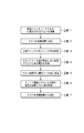
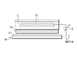
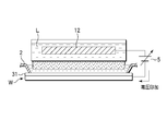
- a Co film serving as a seed layer is formed on a substrate by CVD, and the negative surface potential of the Co is lower than the oxidation potential of Co relative to the substrate. And then, with the negative voltage applied to the substrate, a plating solution mainly composed of a copper sulfate solution is immersed in the Co film, and electrolytic plating is performed on the Co film on the substrate. Forming a Cu film on the substrate.
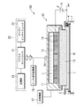
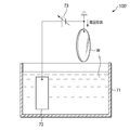
- a DC power source 5 is connected between the wafer W serving as a cathode electrode and the anode electrode 12.
- the negative electrode of the DC power source 5 is connected to the wafer W through the electrode contact 4, and the positive electrode of the DC power source 5 is connected to the anode electrode 12.
- the DC power supply 5 has a variable output voltage.
- FIG. 2 is a flowchart for explaining a film forming method according to an embodiment of the present invention.
- the method of this embodiment is effective when the thickness of the Co film is 5 nm or less.
- the thickness of the Co film can be set in consideration of that amount. preferable. Therefore, the thickness of the Co film is preferably in the range of 1.5 to 5 nm.
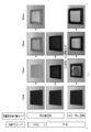
- Example> A sample in which a Co film as a plating seed is formed on a substrate with a thickness of 10 nm and a sample with a thickness of 5 nm are prepared. First, without applying a voltage before immersing these samples in a plating solution A Cu film was formed by electrolytic plating. Further, for a sample on which a Co film having a thickness of 5 nm was formed, a voltage of ⁇ 20 V was applied before being immersed in the plating solution, and then a Cu film was formed by electrolytic plating.
Landscapes
- Chemical & Material Sciences (AREA)
- Engineering & Computer Science (AREA)
- Chemical Kinetics & Catalysis (AREA)
- Electrochemistry (AREA)
- Materials Engineering (AREA)
- Metallurgy (AREA)
- Organic Chemistry (AREA)
- Life Sciences & Earth Sciences (AREA)
- Sustainable Development (AREA)
- Automation & Control Theory (AREA)
- Electrodes Of Semiconductors (AREA)
- Electroplating Methods And Accessories (AREA)
Priority Applications (1)
| Application Number | Priority Date | Filing Date | Title |
|---|---|---|---|
| US13/054,331 US20110174630A1 (en) | 2009-09-17 | 2010-08-27 | Film formation method and storage medium |
Applications Claiming Priority (2)
| Application Number | Priority Date | Filing Date | Title |
|---|---|---|---|
| JP2009-215415 | 2009-09-17 | ||
| JP2009215415A JP2011063849A (ja) | 2009-09-17 | 2009-09-17 | 成膜方法および記憶媒体 |
Publications (1)
| Publication Number | Publication Date |
|---|---|
| WO2011033916A1 true WO2011033916A1 (ja) | 2011-03-24 |
Family
ID=43758525
Family Applications (1)
| Application Number | Title | Priority Date | Filing Date |
|---|---|---|---|
| PCT/JP2010/064572 Ceased WO2011033916A1 (ja) | 2009-09-17 | 2010-08-27 | 成膜方法および記憶媒体 |
Country Status (5)
| Country | Link |
|---|---|
| US (1) | US20110174630A1 (https=) |
| JP (1) | JP2011063849A (https=) |
| KR (1) | KR20110056455A (https=) |
| TW (1) | TW201124564A (https=) |
| WO (1) | WO2011033916A1 (https=) |
Families Citing this family (5)
| Publication number | Priority date | Publication date | Assignee | Title |
|---|---|---|---|---|
| US8858774B2 (en) | 2008-11-07 | 2014-10-14 | Novellus Systems, Inc. | Electroplating apparatus for tailored uniformity profile |
| JP5225957B2 (ja) * | 2009-09-17 | 2013-07-03 | 東京エレクトロン株式会社 | 成膜方法および記憶媒体 |
| JP5659041B2 (ja) * | 2011-02-24 | 2015-01-28 | 東京エレクトロン株式会社 | 成膜方法および記憶媒体 |
| US9909228B2 (en) * | 2012-11-27 | 2018-03-06 | Lam Research Corporation | Method and apparatus for dynamic current distribution control during electroplating |
| JP6678490B2 (ja) * | 2016-03-28 | 2020-04-08 | 株式会社荏原製作所 | めっき方法 |
Citations (4)
| Publication number | Priority date | Publication date | Assignee | Title |
|---|---|---|---|---|
| JP2000355798A (ja) * | 1999-06-15 | 2000-12-26 | Dainippon Screen Mfg Co Ltd | 基板メッキ装置 |
| JP2001123291A (ja) * | 1999-10-25 | 2001-05-08 | Hitachi Ltd | めっき方法及び装置 |
| JP2007534175A (ja) * | 2004-04-21 | 2007-11-22 | インテル・コーポレーション | 感光性誘電体層を分解することによる相互接続構造の形成 |
| JP2008007830A (ja) * | 2006-06-30 | 2008-01-17 | Fujitsu Ltd | めっき方法 |
Family Cites Families (2)
| Publication number | Priority date | Publication date | Assignee | Title |
|---|---|---|---|---|
| US20050006245A1 (en) * | 2003-07-08 | 2005-01-13 | Applied Materials, Inc. | Multiple-step electrodeposition process for direct copper plating on barrier metals |
| US20040245107A1 (en) * | 2003-06-03 | 2004-12-09 | Guangli Che | Method for improving electroplating in sub-0.1um interconnects by adjusting immersion conditions |
-
2009
- 2009-09-17 JP JP2009215415A patent/JP2011063849A/ja not_active Withdrawn
-
2010
- 2010-08-27 KR KR1020107026850A patent/KR20110056455A/ko not_active Ceased
- 2010-08-27 WO PCT/JP2010/064572 patent/WO2011033916A1/ja not_active Ceased
- 2010-08-27 US US13/054,331 patent/US20110174630A1/en not_active Abandoned
- 2010-09-16 TW TW099131353A patent/TW201124564A/zh unknown
Patent Citations (4)
| Publication number | Priority date | Publication date | Assignee | Title |
|---|---|---|---|---|
| JP2000355798A (ja) * | 1999-06-15 | 2000-12-26 | Dainippon Screen Mfg Co Ltd | 基板メッキ装置 |
| JP2001123291A (ja) * | 1999-10-25 | 2001-05-08 | Hitachi Ltd | めっき方法及び装置 |
| JP2007534175A (ja) * | 2004-04-21 | 2007-11-22 | インテル・コーポレーション | 感光性誘電体層を分解することによる相互接続構造の形成 |
| JP2008007830A (ja) * | 2006-06-30 | 2008-01-17 | Fujitsu Ltd | めっき方法 |
Also Published As
| Publication number | Publication date |
|---|---|
| TW201124564A (en) | 2011-07-16 |
| US20110174630A1 (en) | 2011-07-21 |
| KR20110056455A (ko) | 2011-05-30 |
| JP2011063849A (ja) | 2011-03-31 |
Similar Documents
| Publication | Publication Date | Title |
|---|---|---|
| TWI404822B (zh) | Film forming method and memory media (2) | |
| EP3070191B1 (en) | Film forming apparatus for metal coating film and film forming method therefor | |
| US8377824B1 (en) | Methods and apparatus for depositing copper on tungsten | |
| JP5023505B2 (ja) | 成膜方法、プラズマ成膜装置及び記憶媒体 | |
| TWI692552B (zh) | 電鍍設備中之電流密度的控制 | |
| US9536745B2 (en) | Tungsten film forming method | |
| JP6268008B2 (ja) | Cu配線の製造方法 | |
| TW201630036A (zh) | 用以描繪金屬氧化物還原的方法及設備 | |
| WO2004067799A1 (ja) | 半導体処理用の載置台装置、成膜装置、及び成膜方法 | |
| JP5208756B2 (ja) | Ti系膜の成膜方法および記憶媒体 | |
| WO2011033916A1 (ja) | 成膜方法および記憶媒体 | |
| JP2022530804A (ja) | 半導体デバイス製造における金属の電着中のシード層の保護 | |
| US20150072538A1 (en) | Method and apparatus for remote plasma treatment for reducing metal oxides on a metal seed layer | |
| JP2010065309A (ja) | Ti系膜の成膜方法および記憶媒体 | |
| US8906808B2 (en) | Etching method | |
| US20090325393A1 (en) | Heat treatment method and heat treatment apparatus | |
| US20240023204A1 (en) | Coated conductor for heater embedded in ceramic | |
| JP2007043038A (ja) | 金属膜の成膜方法、成膜装置及び記憶媒体 | |
| JP6584326B2 (ja) | Cu配線の製造方法 | |
| JP7564957B2 (ja) | 基板処理方法及び基板処理装置 | |
| US10508351B2 (en) | Layer-by-layer deposition using hydrogen | |
| US8721846B2 (en) | Method of forming film, film forming apparatus and storage medium | |
| WO2008051359A1 (en) | Apparatus and method for substrate electroless plating | |
| WO2010103881A1 (ja) | Cu膜の成膜方法および記憶媒体 | |
| JP2009516775A (ja) | 液晶ディスプレイ用のガラス基板上に、パターン形成された導電層を作成するための方法および装置 |
Legal Events
| Date | Code | Title | Description |
|---|---|---|---|
| ENP | Entry into the national phase |
Ref document number: 20107026850 Country of ref document: KR Kind code of ref document: A |
|
| WWE | Wipo information: entry into national phase |
Ref document number: 13054331 Country of ref document: US |
|
| 121 | Ep: the epo has been informed by wipo that ep was designated in this application |
Ref document number: 10817029 Country of ref document: EP Kind code of ref document: A1 |
|
| NENP | Non-entry into the national phase |
Ref country code: DE |
|
| 122 | Ep: pct application non-entry in european phase |
Ref document number: 10817029 Country of ref document: EP Kind code of ref document: A1 |