JP6678490B2 - めっき方法 - Google Patents
めっき方法 Download PDFInfo
- Publication number
- JP6678490B2 JP6678490B2 JP2016063760A JP2016063760A JP6678490B2 JP 6678490 B2 JP6678490 B2 JP 6678490B2 JP 2016063760 A JP2016063760 A JP 2016063760A JP 2016063760 A JP2016063760 A JP 2016063760A JP 6678490 B2 JP6678490 B2 JP 6678490B2
- Authority
- JP
- Japan
- Prior art keywords
- plating
- substrate
- bump
- plating solution
- height
- Prior art date
- Legal status (The legal status is an assumption and is not a legal conclusion. Google has not performed a legal analysis and makes no representation as to the accuracy of the status listed.)
- Active
Links
Images


Classifications
-
- C—CHEMISTRY; METALLURGY
- C25—ELECTROLYTIC OR ELECTROPHORETIC PROCESSES; APPARATUS THEREFOR
- C25D—PROCESSES FOR THE ELECTROLYTIC OR ELECTROPHORETIC PRODUCTION OF COATINGS; ELECTROFORMING; APPARATUS THEREFOR
- C25D21/00—Processes for servicing or operating cells for electrolytic coating
- C25D21/12—Process control or regulation
-
- C—CHEMISTRY; METALLURGY
- C25—ELECTROLYTIC OR ELECTROPHORETIC PROCESSES; APPARATUS THEREFOR
- C25D—PROCESSES FOR THE ELECTROLYTIC OR ELECTROPHORETIC PRODUCTION OF COATINGS; ELECTROFORMING; APPARATUS THEREFOR
- C25D5/00—Electroplating characterised by the process; Pretreatment or after-treatment of workpieces
- C25D5/02—Electroplating of selected surface areas
-
- C—CHEMISTRY; METALLURGY
- C25—ELECTROLYTIC OR ELECTROPHORETIC PROCESSES; APPARATUS THEREFOR
- C25D—PROCESSES FOR THE ELECTROLYTIC OR ELECTROPHORETIC PRODUCTION OF COATINGS; ELECTROFORMING; APPARATUS THEREFOR
- C25D21/00—Processes for servicing or operating cells for electrolytic coating
- C25D21/02—Heating or cooling
-
- C—CHEMISTRY; METALLURGY
- C25—ELECTROLYTIC OR ELECTROPHORETIC PROCESSES; APPARATUS THEREFOR
- C25D—PROCESSES FOR THE ELECTROLYTIC OR ELECTROPHORETIC PRODUCTION OF COATINGS; ELECTROFORMING; APPARATUS THEREFOR
- C25D21/00—Processes for servicing or operating cells for electrolytic coating
- C25D21/10—Agitating of electrolytes; Moving of racks
-
- C—CHEMISTRY; METALLURGY
- C25—ELECTROLYTIC OR ELECTROPHORETIC PROCESSES; APPARATUS THEREFOR
- C25D—PROCESSES FOR THE ELECTROLYTIC OR ELECTROPHORETIC PRODUCTION OF COATINGS; ELECTROFORMING; APPARATUS THEREFOR
- C25D3/00—Electroplating: Baths therefor
- C25D3/02—Electroplating: Baths therefor from solutions
- C25D3/38—Electroplating: Baths therefor from solutions of copper
-
- C—CHEMISTRY; METALLURGY
- C25—ELECTROLYTIC OR ELECTROPHORETIC PROCESSES; APPARATUS THEREFOR
- C25D—PROCESSES FOR THE ELECTROLYTIC OR ELECTROPHORETIC PRODUCTION OF COATINGS; ELECTROFORMING; APPARATUS THEREFOR
- C25D7/00—Electroplating characterised by the article coated
- C25D7/12—Semiconductors
- C25D7/123—Semiconductors first coated with a seed layer or a conductive layer
-
- H—ELECTRICITY
- H05—ELECTRIC TECHNIQUES NOT OTHERWISE PROVIDED FOR
- H05K—PRINTED CIRCUITS; CASINGS OR CONSTRUCTIONAL DETAILS OF ELECTRIC APPARATUS; MANUFACTURE OF ASSEMBLAGES OF ELECTRICAL COMPONENTS
- H05K3/00—Apparatus or processes for manufacturing printed circuits
- H05K3/10—Apparatus or processes for manufacturing printed circuits in which conductive material is applied to the insulating support in such a manner as to form the desired conductive pattern
- H05K3/18—Apparatus or processes for manufacturing printed circuits in which conductive material is applied to the insulating support in such a manner as to form the desired conductive pattern using precipitation techniques to apply the conductive material
- H05K3/188—Apparatus or processes for manufacturing printed circuits in which conductive material is applied to the insulating support in such a manner as to form the desired conductive pattern using precipitation techniques to apply the conductive material by direct electroplating
-
- H—ELECTRICITY
- H05—ELECTRIC TECHNIQUES NOT OTHERWISE PROVIDED FOR
- H05K—PRINTED CIRCUITS; CASINGS OR CONSTRUCTIONAL DETAILS OF ELECTRIC APPARATUS; MANUFACTURE OF ASSEMBLAGES OF ELECTRICAL COMPONENTS
- H05K3/00—Apparatus or processes for manufacturing printed circuits
- H05K3/40—Forming printed elements for providing electric connections to or between printed circuits
- H05K3/4007—Surface contacts, e.g. bumps
-
- H—ELECTRICITY
- H10—SEMICONDUCTOR DEVICES; ELECTRIC SOLID-STATE DEVICES NOT OTHERWISE PROVIDED FOR
- H10W—GENERIC PACKAGES, INTERCONNECTIONS, CONNECTORS OR OTHER CONSTRUCTIONAL DETAILS OF DEVICES COVERED BY CLASS H10
- H10W72/00—Interconnections or connectors in packages
- H10W72/01—Manufacture or treatment
- H10W72/0198—Manufacture or treatment batch processes
-
- H—ELECTRICITY
- H10—SEMICONDUCTOR DEVICES; ELECTRIC SOLID-STATE DEVICES NOT OTHERWISE PROVIDED FOR
- H10W—GENERIC PACKAGES, INTERCONNECTIONS, CONNECTORS OR OTHER CONSTRUCTIONAL DETAILS OF DEVICES COVERED BY CLASS H10
- H10W72/00—Interconnections or connectors in packages
- H10W72/01—Manufacture or treatment
- H10W72/012—Manufacture or treatment of bump connectors, dummy bumps or thermal bumps
- H10W72/01231—Manufacture or treatment of bump connectors, dummy bumps or thermal bumps using blanket deposition
- H10W72/01233—Manufacture or treatment of bump connectors, dummy bumps or thermal bumps using blanket deposition in liquid form, e.g. spin coating, spray coating or immersion coating
- H10W72/01235—Manufacture or treatment of bump connectors, dummy bumps or thermal bumps using blanket deposition in liquid form, e.g. spin coating, spray coating or immersion coating by plating, e.g. electroless plating or electroplating
-
- H—ELECTRICITY
- H10—SEMICONDUCTOR DEVICES; ELECTRIC SOLID-STATE DEVICES NOT OTHERWISE PROVIDED FOR
- H10W—GENERIC PACKAGES, INTERCONNECTIONS, CONNECTORS OR OTHER CONSTRUCTIONAL DETAILS OF DEVICES COVERED BY CLASS H10
- H10W72/00—Interconnections or connectors in packages
- H10W72/20—Bump connectors, e.g. solder bumps or copper pillars; Dummy bumps; Thermal bumps
- H10W72/251—Materials
- H10W72/252—Materials comprising solid metals or solid metalloids, e.g. PbSn, Ag or Cu
Landscapes
- Chemical & Material Sciences (AREA)
- Engineering & Computer Science (AREA)
- Organic Chemistry (AREA)
- Electrochemistry (AREA)
- Materials Engineering (AREA)
- Metallurgy (AREA)
- Chemical Kinetics & Catalysis (AREA)
- Manufacturing & Machinery (AREA)
- Microelectronics & Electronic Packaging (AREA)
- Automation & Control Theory (AREA)
- Electroplating Methods And Accessories (AREA)
- Electroplating And Plating Baths Therefor (AREA)
- Electrodes Of Semiconductors (AREA)
Description
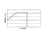
本発明の好ましい態様は、前記基板のめっき開始時に、電流密度を上昇させることを特徴とする。
本発明の好ましい態様は、前記電流密度は、1A/dm2から20A/dm2の範囲内であることを特徴とする。
本発明の好ましい態様は、前記基板のめっき中の前記めっき液の温度を30℃から80℃の範囲内に維持することを特徴とする。
本発明の好ましい態様は、前記基板のめっき中に、パドルを前記めっき液中で往復運動させることによって前記めっき液を攪拌し、前記パドルの往復動速度は、100回/分から500回/分の範囲内であることを特徴とする。
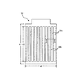
12 オーバーフロー槽
14 ポンプ
16 めっき液供給ライン
20 温調ユニット
22 フィルタ
24 基板ホルダ
26 アノード
28 アノードホルダ
30 電源
32 パドル
34 調整板
Claims (6)
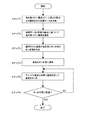
- 基板を銅でめっきしてバンプを形成する方法であって、
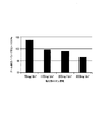
バンプ高さに対するドーム高さの割合と、塩化物イオンの濃度との関係を示す相関データを用意し、前記相関データは、バンプを形成するためのめっき装置の記憶装置に記憶されており、
バンプ高さに対するドーム高さの所望の割合と、前記相関データとに基づいて選択された濃度の塩化物イオンを含むめっき液を作成し、前記選択された濃度は、100mg/dm3〜300mg/dm3の範囲内であり、
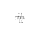
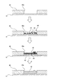
基板を前記めっき液中に浸漬させ、前記基板は、シード層と、該シード層上に形成されたレジストを有し、前記レジストは開口部を有し、前記開口部の側壁は前記レジストにより構成され、前記開口部の底部は前記シード層の露出面から構成されており、
前記めっき液中のアノードと前記基板との間に電流を流して前記基板をめっきすることで、前記開口部内の前記シード層の露出面上にバンプを形成することを特徴とする方法。 - バンプの高さが少なくとも100μmに達するまで、前記基板のめっきを行うことを特徴とする請求項1に記載の方法。
- 前記基板のめっき開始時に、電流密度を上昇させることを特徴とする請求項1または2に記載の方法。
- 前記電流密度は、1A/dm2から20A/dm2の範囲内であることを特徴とする請求項3に記載の方法。
- 前記基板のめっき中の前記めっき液の温度を30℃から80℃の範囲内に維持することを特徴とする請求項1乃至4のいずれか一項に記載の方法。
- 前記基板のめっき中に、パドルを前記めっき液中で往復運動させることによって前記めっき液を攪拌し、前記パドルの往復動速度は、100回/分から500回/分の範囲内であることを特徴とする請求項1乃至5のいずれか一項に記載の方法。
Priority Applications (4)
| Application Number | Priority Date | Filing Date | Title |
|---|---|---|---|
| JP2016063760A JP6678490B2 (ja) | 2016-03-28 | 2016-03-28 | めっき方法 |
| KR1020170036042A KR102061026B1 (ko) | 2016-03-28 | 2017-03-22 | 도금 방법 |
| TW106109516A TWI699838B (zh) | 2016-03-28 | 2017-03-22 | 鍍覆方法 |
| US15/466,282 US10468364B2 (en) | 2016-03-28 | 2017-03-22 | Plating method |
Applications Claiming Priority (1)
| Application Number | Priority Date | Filing Date | Title |
|---|---|---|---|
| JP2016063760A JP6678490B2 (ja) | 2016-03-28 | 2016-03-28 | めっき方法 |
Publications (2)
| Publication Number | Publication Date |
|---|---|
| JP2017183332A JP2017183332A (ja) | 2017-10-05 |
| JP6678490B2 true JP6678490B2 (ja) | 2020-04-08 |
Family
ID=59898942
Family Applications (1)
| Application Number | Title | Priority Date | Filing Date |
|---|---|---|---|
| JP2016063760A Active JP6678490B2 (ja) | 2016-03-28 | 2016-03-28 | めっき方法 |
Country Status (4)
| Country | Link |
|---|---|
| US (1) | US10468364B2 (ja) |
| JP (1) | JP6678490B2 (ja) |
| KR (1) | KR102061026B1 (ja) |
| TW (1) | TWI699838B (ja) |
Families Citing this family (4)
| Publication number | Priority date | Publication date | Assignee | Title |
|---|---|---|---|---|
| JP6970346B2 (ja) | 2018-09-25 | 2021-11-24 | 日亜化学工業株式会社 | 半導体装置の製造方法 |
| JP7183111B2 (ja) * | 2019-05-17 | 2022-12-05 | 株式会社荏原製作所 | めっき方法、めっき用の不溶性アノード、及びめっき装置 |
| KR102447745B1 (ko) * | 2021-03-05 | 2022-09-28 | 가부시키가이샤 에바라 세이사꾸쇼 | 도금 모듈을 조정하는 방법 |
| CN117867614B (zh) * | 2024-03-11 | 2024-07-09 | 武创芯研科技(武汉)有限公司 | 一种芯片铜柱的电镀方法及铜柱凸块的制作方法 |
Family Cites Families (10)
| Publication number | Priority date | Publication date | Assignee | Title |
|---|---|---|---|---|
| JP2006131961A (ja) * | 2004-11-05 | 2006-05-25 | Ebara Corp | 基板のめっき方法および装置 |
| US20070215479A1 (en) * | 2006-03-15 | 2007-09-20 | Rockwood Electrochemicals Asia Ltd. | Method for monitoring the filling performance of copper plating formula for microvia filling |
| US7575666B2 (en) | 2006-04-05 | 2009-08-18 | James Watkowski | Process for electrolytically plating copper |
| JP5184308B2 (ja) * | 2007-12-04 | 2013-04-17 | 株式会社荏原製作所 | めっき装置及びめっき方法 |
| JP2010255078A (ja) | 2009-04-28 | 2010-11-11 | Adeka Corp | 電解銅めっき浴および電解銅めっき方法 |
| JP2011054890A (ja) | 2009-09-04 | 2011-03-17 | Ebara Corp | バンプ形成方法及び接合方法 |
| JP2011063849A (ja) * | 2009-09-17 | 2011-03-31 | Tokyo Electron Ltd | 成膜方法および記憶媒体 |
| US10472730B2 (en) | 2009-10-12 | 2019-11-12 | Novellus Systems, Inc. | Electrolyte concentration control system for high rate electroplating |
| US20160102416A1 (en) * | 2013-01-29 | 2016-04-14 | Novellus Systems, Inc. | Low copper/high halide electroplating solutions for fill and defect control |
| JP6356119B2 (ja) * | 2013-04-02 | 2018-07-11 | 株式会社Adeka | 電解銅めっき浴用添加剤、該添加剤を含む電解銅めっき浴および該電解銅めっき浴を用いた電解銅めっき方法 |
-
2016
- 2016-03-28 JP JP2016063760A patent/JP6678490B2/ja active Active
-
2017
- 2017-03-22 KR KR1020170036042A patent/KR102061026B1/ko active Active
- 2017-03-22 TW TW106109516A patent/TWI699838B/zh active
- 2017-03-22 US US15/466,282 patent/US10468364B2/en active Active
Also Published As
| Publication number | Publication date |
|---|---|
| KR102061026B1 (ko) | 2019-12-31 |
| US10468364B2 (en) | 2019-11-05 |
| TWI699838B (zh) | 2020-07-21 |
| KR20170113180A (ko) | 2017-10-12 |
| TW201801206A (zh) | 2018-01-01 |
| JP2017183332A (ja) | 2017-10-05 |
| US20170278813A1 (en) | 2017-09-28 |
Similar Documents
| Publication | Publication Date | Title |
|---|---|---|
| CN100416777C (zh) | 在半导体应用的电沉积铜中缺陷的降低 | |
| US12424453B2 (en) | Low temperature direct copper-copper bonding | |
| JP4758614B2 (ja) | 電気めっき組成物および方法 | |
| JP6960502B2 (ja) | 改善された完全性を有する銅ピラーおよびその製造方法 | |
| JP6678490B2 (ja) | めっき方法 | |
| CN104674311A (zh) | 镀液和镀覆方法 | |
| CN104651893A (zh) | 用于电镀的碱预处理 | |
| JP5281831B2 (ja) | 導電材料構造体の形成方法 | |
| JP2017036500A (ja) | イミダゾールとビスエポキシド化合物との反応生成物を含有する電気銅めっき浴からフォトレジスト画定フィーチャを電気めっきする方法 | |
| TW201444004A (zh) | 半導體結構及其製造方法 | |
| JP2017036501A5 (ja) | ||
| TWI451006B (zh) | 導電性結構之形成方法、鍍覆裝置及鍍覆方法 | |
| EP3263745B1 (en) | Method of electroplating photoresist defined features from copper electroplating baths containing reaction products of pyrazole compounds and bisepoxides | |
| KR101818655B1 (ko) | 실리콘 관통전극의 무결함 충전방법 및 충전방법에 사용되는 구리 도금액 | |
| TWI802603B (zh) | 單一金屬之多浴電鍍 | |
| KR20190052612A (ko) | 구리 전기도금 조성물 및 기판에서 구리의 전기도금 방법 | |
| JP2013168679A (ja) | 導電材料構造体の形成方法 | |
| JP4553632B2 (ja) | 基板めっき方法及び基板めっき装置 | |
| US20060163058A1 (en) | Apparatus for plating a semiconductor wafer and plating solution bath used therein | |
| KR20150119987A (ko) | Tsv 충전용 전해 구리 도금액 및 이를 이용한 tsv의 충전방법 | |
| KR101596437B1 (ko) | 플립칩 패키지 구리 필라의 제조 방법과 이를 위한 동계 전기도금액 | |
| Jensen et al. | Conformal Open-Air Electroplating of Through-Wafer Vias | |
| CN121110130A (zh) | 用于制备含锑的锡基合金封装凸点结构的电镀液和电镀方法 |
Legal Events
| Date | Code | Title | Description |
|---|---|---|---|
| A621 | Written request for application examination |
Free format text: JAPANESE INTERMEDIATE CODE: A621 Effective date: 20181018 |
|
| A131 | Notification of reasons for refusal |
Free format text: JAPANESE INTERMEDIATE CODE: A131 Effective date: 20190618 |
|
| A977 | Report on retrieval |
Free format text: JAPANESE INTERMEDIATE CODE: A971007 Effective date: 20190620 |
|
| A601 | Written request for extension of time |
Free format text: JAPANESE INTERMEDIATE CODE: A601 Effective date: 20190731 |
|
| A521 | Request for written amendment filed |
Free format text: JAPANESE INTERMEDIATE CODE: A523 Effective date: 20191011 |
|
| TRDD | Decision of grant or rejection written | ||
| A01 | Written decision to grant a patent or to grant a registration (utility model) |
Free format text: JAPANESE INTERMEDIATE CODE: A01 Effective date: 20200225 |
|
| A61 | First payment of annual fees (during grant procedure) |
Free format text: JAPANESE INTERMEDIATE CODE: A61 Effective date: 20200317 |
|
| R150 | Certificate of patent or registration of utility model |
Ref document number: 6678490 Country of ref document: JP Free format text: JAPANESE INTERMEDIATE CODE: R150 |
|
| R250 | Receipt of annual fees |
Free format text: JAPANESE INTERMEDIATE CODE: R250 |
|
| R250 | Receipt of annual fees |
Free format text: JAPANESE INTERMEDIATE CODE: R250 |
|
| R250 | Receipt of annual fees |
Free format text: JAPANESE INTERMEDIATE CODE: R250 |
|
| R250 | Receipt of annual fees |
Free format text: JAPANESE INTERMEDIATE CODE: R250 |