WO2011024945A1 - ウエハレンズの製造方法 - Google Patents
ウエハレンズの製造方法 Download PDFInfo
- Publication number
- WO2011024945A1 WO2011024945A1 PCT/JP2010/064581 JP2010064581W WO2011024945A1 WO 2011024945 A1 WO2011024945 A1 WO 2011024945A1 JP 2010064581 W JP2010064581 W JP 2010064581W WO 2011024945 A1 WO2011024945 A1 WO 2011024945A1
- Authority
- WO
- WIPO (PCT)
- Prior art keywords
- wafer
- lens
- identification information
- wafer lens
- inspection
- Prior art date
- Legal status (The legal status is an assumption and is not a legal conclusion. Google has not performed a legal analysis and makes no representation as to the accuracy of the status listed.)
- Ceased
Links
Images




Classifications
-
- G—PHYSICS
- G02—OPTICS
- G02B—OPTICAL ELEMENTS, SYSTEMS OR APPARATUS
- G02B13/00—Optical objectives specially designed for the purposes specified below
- G02B13/001—Miniaturised objectives for electronic devices, e.g. portable telephones, webcams, PDAs, small digital cameras
- G02B13/0085—Miniaturised objectives for electronic devices, e.g. portable telephones, webcams, PDAs, small digital cameras employing wafer level optics
-
- B—PERFORMING OPERATIONS; TRANSPORTING
- B29—WORKING OF PLASTICS; WORKING OF SUBSTANCES IN A PLASTIC STATE IN GENERAL
- B29L—INDEXING SCHEME ASSOCIATED WITH SUBCLASS B29C, RELATING TO PARTICULAR ARTICLES
- B29L2011/00—Optical elements, e.g. lenses, prisms
Definitions
- the present invention relates to a wafer lens and a method for manufacturing the wafer lens.
- a diaphragm made of a metal film on the surface of a glass flat plate for adjusting the amount of incident light is formed, and an optical member made of a cured resin is formed on the surface of the diaphragm.
- a plurality of so-called “wafer lenses” are formed. After that, in a state where a plurality of lenses are integrated, a spacer is sandwiched, and a protrusion formed simultaneously with the optical surface is abutted and stacked, and bonded to form a plurality of assembled lenses.
- a method of cutting the flat plate portion has been developed. According to this manufacturing method, the manufacturing cost of the optical lens can be reduced.
- such a wafer lens and a plurality of group lenses are cut into individual pieces and attached to an image sensor, or a sensor wafer that is also formed into a wafer is cut into individual pieces after being joined to the wafer lens or the plurality of group lenses. It is also attracting attention in that it can mass-produce small and high-resolution imaging units including image sensors.
- the diaphragm formed on the glass flat plate is usually formed by repeatedly performing operations such as etching, vapor deposition, and plating after forming a resist pattern on the surface of the glass flat plate using well-known photolithography.
- operations such as etching, vapor deposition, and plating after forming a resist pattern on the surface of the glass flat plate using well-known photolithography.
- the above method has a large number of steps, it is required to be further simplified.
- the manufacturing process can be improved by performing the inspection process for each lens in the state of a single wafer or in the state of an assembly in which a plurality of wafers are combined. It is done.
- the present invention has been made in view of the above problems in the prior art, and a wafer lens manufacturing method and lens inspection information in which the occurrence of defective lenses is reduced by effectively utilizing inspection information obtained in the inspection process. It is an object of the present invention to provide a wafer lens suitable for individual information management, such as a wafer lens, and a wafer lens manufacturing method capable of favorably performing lens inspection information management.
- a method for manufacturing a wafer lens in which an optical member made of a curable resin is formed on a substrate, and the back of each lens unit on the wafer.
- a method for manufacturing a wafer lens comprising: a step of measuring a focus; a step of selecting a spacer having an optimum thickness to be combined with the wafer based on a measurement result of the back focus; and a step of bonding the wafer to the selected spacer. is there.
- the step of selecting a spacer having an optimum thickness to be combined with the wafer based on the measurement result of the back focus includes information for identifying an optimum spacer to be selected, and the optimum spacer. It is preferable to include a step of recording, in the data file, information for specifying a lens unit that is out of specification when selected.
- a wafer lens in which an optical member made of a curable resin is formed on a substrate, and an aperture that serves as an optical component on the substrate, and individual identification information of the wafer lens.
- a wafer lens in which a recorded identification information recording portion is laid and the diaphragm and the identification information recording portion are covered with a resin layer forming the optical member.
- the diaphragm and the identification information recording unit are formed of the same material arranged in the same layer.
- the same material is a light-shielding photoresist.
- the third aspect of the present invention is a lamination step of laminating the same material layer constituting an aperture serving as an optical component and an identification information recording unit in which individual identification information of a wafer lens is recorded on a substrate, A patterning step of selectively removing the same material layer by patterning to form the diaphragm; An identification information recording step of selectively processing the same material layer with a laser marker to form the identification information recording unit; A curable resin is filled between the surface of the substrate on which the diaphragm and the identification information recording unit are formed, and a mold, and an optical member is molded using the curable resin as a material by the mold. A molding step for covering the aperture and the identification information recording part with the curable resin, And a curing step for curing the curable resin.
- the same material layer in the laminating step is a light-shielding resist layer, and in the patterning step, the light-shielding resist layer is exposed and developed, and then in the identification information recording step, It is preferable to form the identification information recording part by selectively removing the light-shielding resist layer.
- an inspection step for inspecting an optical member formed on the wafer lens an identification information reading step for reading individual identification information of the wafer lens from the identification information recording unit, It is preferable to include a storage step of storing inspection information in the inspection step in a management server in association with the individual identification information related to the wafer lens to be inspected.
- component identification information for specifying individual optical members is set in advance for each optical member formation region on the wafer lens, and inspection information for each optical member in the inspection process is set as the wafer lens to which the optical component to be inspected belongs. It is also preferable to include a storage step of storing in the management server in association with the individual identification information according to the above and the component identification information regarding the optical member to be inspected.
- a surface map of the wafer lens is displayed on the image display device, and based on the individual identification information, the component identification information, and the inspection information associated therewith, the inspection information of the optical member is optically inspected on the surface map. It is preferable that a display step of displaying at a position corresponding to the member formation region is provided.
- a visual display indicating that the optical member is not inspected is formed by selectively processing the optical member with a laser marker for an optical member that is determined to be an inspection-invalid product based on the inspection information. It is also preferable to have an inspection failure recording step.
- the spacer having the optimum thickness to be combined with the wafer is selected based on the measurement result of the back focus of each lens unit on the wafer, the generation of defective lenses is prevented. Can be reduced.
- the individual wafer lens can be identified by reading the individual identification information of the wafer lens from the identification information recording unit by the reading device. It is possible to satisfactorily manage individual information such as lens inspection information.
- a diaphragm serving as an optical component and an identification information recording unit in which individual identification information of the wafer lens is recorded are laid on a substrate, and the diaphragm and the identification information recording unit are formed by a resin layer that forms an optical member. Since it is covered, the identification information recording unit is protected, so that the information storability and tampering prevention of the identification information recording unit are improved.
- the coating layer of the identification information recording part is composed of the resin layer forming the optical member, there is no increase in the number of processes and materials for constituting the coating layer of the identification information recording part.
- the diaphragm and the identification information recording part are formed of the same material arranged in the same layer, so that the constituent material layer of the identification information recording part can be laminated in the same process as the lamination of the constituent material layers of the diaphragm. There is no increase in the number of steps and materials for laminating the constituent material layers.
- the manufacturing process can be simplified as compared with a conventional metal film.
- the wafer lens of the present invention in which individual identification information of the wafer lens is recorded can be manufactured, and the same effects as described above can be obtained.
- the inspection information management of the lens can be performed satisfactorily.
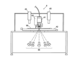
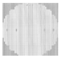
- 1 is a cross-sectional view (corresponding to a line AA) of a group wafer lens according to an embodiment of the present invention. It is a quarter top view of the 2nd wafer lens concerning one embodiment of the present invention. It is a block diagram which shows the flow of the manufacturing method (a test process is included) of the wafer lens which concerns on one Embodiment of this invention. It is a block diagram of the MTF / FB inspection machine which concerns on one Embodiment of this invention. It is detail drawing of the light source part of the MTF / FB inspection machine shown in FIG.
- the wafer lens of the present invention is implemented on the first wafer lens and the second wafer lens.
- Individual identification information (hereinafter referred to as “wafer ID”) of the wafer lens according to the present invention is attached to the first wafer lens L1 and the second wafer lens L2.
- the first wafer lens L1 includes a glass substrate 10, and a diaphragm 11a and an ID recording unit 11b formed on one surface of the glass substrate 10.
- a large number of stops 11a, 11a, 11a,... Are formed in most of the center on the glass substrate 10.
- An ID recording portion 11b is formed in the periphery of a large number of apertures 11a, 11a, 11a,.
- the diaphragm 11a and the ID recording part 11b are formed of the same material arranged in the same layer 11, and a light-shielding photoresist is applied in this embodiment.
- a light-shielding photoresist a photoresist mixed with carbon black is applied.
- the ID recording unit 11b is composed of a two-dimensional barcode. Information is recorded in the ID recording unit 11b in a binary representation of a predetermined number of digits, and this information includes the wafer ID of the first wafer lens L1. This information can be read by a barcode reader.
- the diaphragm 11a and the ID recording portion 11b are covered with a photo-curable resin layer 12 that forms an optical member 12a and the like.
- the resin layer 12 is formed on the surface of the glass substrate 10 on which the aperture 11a and the ID recording portion 11b are formed, and constitutes a convex lens portion 12a, a lens peripheral protrusion 12b, and a peripheral flat plate portion 12c.
- the diaphragm 11a is covered with a convex lens portion 12a, a lens peripheral protrusion 12b, and the like, and the ID recording portion 11b is covered with a peripheral flat plate portion 12c.
- a resin layer 13 is formed on the surface of the glass substrate 10 opposite to the resin layer 12.
- the resin layer 13 constitutes a concave lens portion 13a at a position coaxial with the convex lens portion 12a.
- a portion formed by one convex lens portion 12a, one diaphragm 11a, and one concave lens portion 13a corresponds to one unit of a component, and is held on the wafer in a large number of other wafer lenses L2, spacers 30, and image sensors (see FIG. (Not shown) and unitized.
- the second wafer lens L2 includes a glass substrate 20, and a diaphragm 21a and an ID recording unit 21b formed on one surface of the glass substrate 20.
- a large number of stops 21 a, 21 a, 21 a,... Are formed in the central part on the glass substrate 20.
- An ID recording portion 21b is formed in the periphery of a large number of apertures 21a, 21a, 21a,.
- the aperture 21a and the ID recording part 21b are formed of the same material arranged in the same layer 21, and a light-shielding photoresist is applied in this embodiment.
- a light-shielding photoresist a photoresist mixed with carbon black is applied.
- the ID recording unit 21b is composed of a two-dimensional barcode. Information is recorded in the ID recording unit 21b in a binary representation of a predetermined number of digits, and this information includes the wafer ID of the second wafer lens L2. This information can be read by a barcode reader.
- the aperture 21a and the ID recording portion 21b are covered with a photo-curable resin layer 22 that forms a convex lens portion 22a and the like.
- the resin layer 22 is formed on the surface of the glass substrate 10 on which the aperture 21a and the ID recording portion 21b are formed, and constitutes a convex lens portion 22a and lens peripheral protrusions 22b and 22c.
- the stop 21a is covered with a convex lens portion 22a, lens peripheral protrusions 22b and 22c, and the ID recording portion 21b is covered with an outer peripheral lens peripheral protrusion 22c.
- a resin layer 23 is formed on the surface of the glass substrate 20 opposite to the resin layer 22.
- the resin layer 23 constitutes a concave lens portion 23a at a position coaxial with the convex lens portion 22a.
- a portion formed by one convex lens portion 22a, one stop 21a, and one concave lens portion 23a corresponds to one unit of a component, and in the state where a large number are held on the wafer, another wafer lens L1, spacer 30, image sensor (see FIG. (Not shown) and unitized.
- the same material layer 11 (21) constituting the diaphragm 11a (21a) serving as an optical component and the ID recording part 11b on which the wafer ID is recorded is laminated (lamination process).
- the material layer 11 a photoresist mixed with carbon black is applied, and this photoresist is applied onto the glass substrate 10.
- the material layer 11 (21) is selectively removed by patterning exposure and subsequent development processing to form a stop 11a (21a) (patterning step).
- the material layer 11 (21) left around the diaphragm 11a (21a) is selectively removed by the laser marker LM1 shown in FIG. 4 to form an ID recording portion 11b (21b) (identification information recording step, Equivalent to blocks A1 and A2.)
- ID recording portion 11b (identification information recording step, Equivalent to blocks A1 and A2.)
- forming the ID recording portion corresponds to recording the wafer ID.
- the laser marker LM1 is controlled by the marker control PC (block MC), and information regarding the wafer ID is held in the marker control PC.
- the marker control PC controls the laser marker LM1 to give a wafer ID to each wafer lens.
- the wafer ID assigned by the marker control PC (block MC) is transmitted from the marker control PC to the server PC (block S), and a data file for each wafer ID is created by the server PC. Manufacturing information such as date of manufacture is recorded in the data file.
- the server PC sets component identification information for specifying the lens on the wafer lens when creating the data file.
- Component identification information for specifying a lens is provided corresponding to each lens on the wafer lens.
- Each lens and its component identification information correspond to each other depending on the position of the lens formation region. That is, address information is set in the formation area of each lens, and this address information is used as identification information for the lens formed there. This eliminates the need to write component identification information for identifying the lens on the product.
- the inspection information for the lens on the wafer lens specified by the wafer ID is stored as manufacturing history information in association with the address information of the lens in the data file to which the wafer ID is attached.
- the process proceeds to the subsequent wafer lens manufacturing process and the process of stacking and combining the two wafer lenses as shown in block B of FIG.
- a photo-curable resin is filled between the surface of the glass substrate 10 (20) on which the diaphragm 11a (21a) and the ID recording unit 11b (21b) are formed and a molding die (not shown), and the light is transmitted by the molding die.
- Optical members convex lens portions 12a and 22a), lens peripheral protrusions 12b (22b and 22c), peripheral flat plate portions 12c and the like are molded using a curable resin as a material, and an aperture 11a (21a) and an ID recording portion 11b (21b) are formed.
- the curable resin molding step. In this step, for example, a resin in a monomer state (before curing) is placed on the glass substrate 10 (20) and the mold is pressed from above.
- the resin is irradiated with light and cured (curing process).
- Light is irradiated from the glass substrate 10 (20) side, or the mold is made of a transparent material such as a transparent resin and irradiated from the mold side.
- the resin layer 13 (23) on the other surface of the glass substrate 10 (20) is similarly molded to complete the first wafer lens L1 and the second wafer lens L2, respectively.
- the surface of the resin layer 13 of the first wafer lens L1 and the resin layer 23 of the second wafer lens L2 are laminated together, and the two wafers are laminated, fixed and bonded to the assembled wafer (L1 + L2).
- the back focus FB of each lens unit on the assembled wafer (L1 + L2) is measured.
- the FB inspection PC (block C1) controls the FB inspection machine to sequentially measure the back focus FB of each lens unit on the assembled wafer (L1 + L2), and uses the attached barcode reader to inspect the assembled wafer (L1 + L2).
- the wafer ID of the second wafer lens L2 is read from the upper ID recording unit 21b and the ID to be inspected is recognized.
- the assembled wafer (L1 + L2) can be specified by either the wafer ID of the first wafer lens L1 or the wafer ID of the second wafer lens L2, so it is sufficient to use either one.
- the wafer ID of the second wafer lens L2 and its data file are used.
- information management related to the first wafer lens L1 single unit is the wafer ID of the first wafer lens L1 and its data file
- information management related to the second wafer lens L2 single unit is the wafer ID of the second wafer lens L2 and its data file. Is used.
- the FB inspection PC downloads the data file of the corresponding ID from the server PC, records the inspection information in the data file, uploads it to the server PC, and the server PC updates the data file.
- the inspection information recorded in the data file by the FB inspection PC includes information for specifying the optimum spacer 30 to be selected and information for specifying a lens unit that will be out of specification when the spacer 30 is selected. (Error information Err).
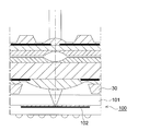
- FIG. 11 shows a state where a lens unit is mounted on the image sensor 100 (CMOS sensor or the like).
- the lens unit is fixed on the image sensor by adhesion between the spacer 30 and the cover glass 101 of the image sensor 100.
- the lens unit has an overfocal length U ⁇ f 2 / (F ⁇ 2 ⁇ P) (where f: focal length of the lens unit, F: F number of the lens unit, P: pixel pitch of the image sensor).
- the thickness of the spacer 30 is set so that the image point of the lens unit and the photoelectric conversion unit 102 of the image sensor coincide with each other, the focus is achieved from a distance of infinity to 46 cm.
- the reference subject distance may be set far from the hyperfocal distance.
- the thickness of the spacer 30 may be slightly reduced.
- the thickness of the spacer 30 for setting the optimum focus needs to be set so that as many FBs as possible of the lens units in the assembled wafer fall within this range.
- a process of polishing the flat glass after measuring the FB average value of the lens units in the assembled wafer and adjusting the thickness of the spacer 30 so that the desired focus position is obtained.
- the back focus FB standard for example, the average value of the FB of all lens units in the assembled wafer is obtained, and the value within the FB allowable variation set in advance while taking into account the depth of focus is within the standard. Record the inspection information as non-standard.
- the spacers 30 selected based on the inspection information recorded in the data file of the ID are combined with the assembled wafer (L1 + L2), and are stacked and bonded and fixed as shown in FIG.
- the MTF / FB inspection PC (block C2) controls the MTF / FB inspection machine 4 shown in FIG. 5 to perform MTF / FB inspection of each lens unit on the assembled wafer (L1 + L2 + spacer 30).
- the MTF / FB inspection machine 4 includes a light source unit 41 that irradiates a lens with predetermined light and a wafer lens WL and is perpendicular to the light irradiation direction (Z axis).
- An automatic XY stage 42 that moves in the Y direction, a distance sensor 43 that is fixed to the light source unit 41 and measures the distance from the lens, a measurement optical system 44 having a plurality of CCD cameras, and wafer rotation adjustment cameras 45 and 45 With.
- the light source unit 41 and the distance sensor 43 fixed to the light source unit 41 are controlled to move in the vertical (Z-axis) direction.
- the light source unit 41 includes a halogen fiber 41a, a bandpass filter 41b, a diffusion plate 41c, and a chart 41d.
- the assembled wafer (L1 + L2 + spacer 30) according to the above manufacturing is placed.
- the MTF / FB inspection PC measures the value of MTF (Modulation Transfer Function) at the center of the lens with one CCD camera of the measurement optical system 44, specifies the FB that maximizes the MTF value by moving the light source unit 41 up and down,
- the FB value is calculated based on the output value of the distance sensor 43, and the MTF values of the lens peripheral part in the FB value are measured by the other four CCD cameras of the measurement optical system 44. Calculate what percentage of the central MTF maximum value.
- the MTF / FB inspection PC controls the MTF / FB inspection machine 4 and performs the above measurement and calculation for each irradiation light of different frequencies.
- the MTF / FB inspection PC selects lens units that are out of specification based on these acquired numerical values.
- the MTF / FB inspection PC reads the wafer ID of the second wafer lens L2 from the ID recording unit 21b on the group wafer (L1 + L2 + spacer 30) to be inspected by the attached barcode reader, and recognizes the ID to be inspected.
- the MTF / FB inspection PC downloads the data file of the corresponding ID from the server PC, records the inspection information in the data file, uploads it to the server PC, and the server PC updates the data file.
- the inspection information recorded in the data file by the MTF / FB inspection PC includes information (error information Err) for specifying a lens unit that is out of specification.
- the correction jig 5 includes a frame body 51 having a vent hole 51 a and a sealing glass 52 that seals one surface of the frame body 51.
- the wafer lens WL is placed on the other surface of the frame body 51. Then, the peripheral edge portion of the wafer lens WL is closely fixed to the frame body 51 and sealed so as not to cause air leakage. As a sealing method, the peripheral edge of the wafer lens WL is mechanically pressed against the frame body 51, or a porous suction disk is built in the part of the frame body 51 where the wafer lens WL is placed. A method of attracting and holding the wafer lens WL and other methods are applied.
- the warp correction jig 5 holding the wafer lens WL is placed on the automatic XY stage 42 of the MTF / FB inspection machine 4.
- the Z-axis direction position of the distance sensor 43 is fixed, the automatic XY stage 42 is moved, and the warpage of the wafer lens WL is measured by the distance sensor 43.
- other equipment may be used.
- any measuring instrument such as the autocollimator 61 shown in FIG. 8, a contact displacement meter 62, or a laser triangulation displacement meter may be used.
- the sealed space 53 is sucked by the air pump through the vent hole 51a, or if the top surface is concave, the air enters the sealed space 53.
- the internal pressure of the sealed space 53 is held to hold the wafer lens WL in a corrected state.
- sealing glass 52 transmits light by sealing the opposite surface of the wafer lens WL with the sealing glass 52, optical measurement on the wafer lens WL can be performed without any trouble.
- the picture inspection PC reads the wafer ID of the second wafer lens L2 from the ID recording unit 21b on the group wafer (L1 + L2 + spacer 30) to be inspected by the attached barcode reader, and recognizes the ID to be inspected.
- the picture inspection PC downloads the data file of the corresponding ID from the server PC, refers to the error information Err at the time of MTF / FB inspection, and excludes lens units that are certified as non-standard in the MTF / FB inspection.
- the image inspection is performed on all the remaining lens units.
- the image inspection PC (block C3) controls the reflection inspection machine 7 shown in FIG. 9 to perform image inspection of each lens unit on the assembled wafer (L1 + L2 + spacer 30).
- the reflection inspection machine 7 includes a measurement head 70 integrally having a CCD 71, a drawing board 72, and a distance sensor 73, and the measurement head 70 is controlled to move in the vertical (Z-axis) direction.
- the reflection inspection machine 7 includes an automatic XY stage 74, a uniform light source 75, and alignment cameras 76 and 76, and the frame 77 and the warp correction jig 5 are shared with the MTF / FB inspection machine 4.
- the picture inspection PC (block C3) includes a motion controller 81, a D / IO board 82, and an image input board 83.
- the motion controller 81 is connected to an actuator for moving the measuring head 70 via a driver 91 and is connected to an actuator for moving the automatic XY stage 74 via a driver 92.
- the D / IO board 82 is connected to the uniform light source 75 and outputs light from the uniform light source 75.
- the image input board 83 is connected to the alignment cameras 76 and 76 and captures images taken by the alignment cameras 76 and 76.
- a distance sensor 73 is also connected to the picture inspection PC.
- the assembled wafer (L1 + L2 + spacer 30) according to the above manufacturing is placed.
- the image inspection PC After the inspection, the image inspection PC records the inspection information in the data file and uploads it to the server PC, and the server PC updates the data file.
- the inspection information recorded in the data file by the image inspection PC includes information (error information Err) for specifying a lens unit that is out of specification.
- the appearance inspection is performed using the appearance inspection photographing PC (block C4), and the image confirmation is performed using the image confirmation PC (block C5).
- These are assumed to be inspected by an inspector, but may be replaced with an inspection by an automatic inspection PC (block D) in which work by these inspectors is automated.
- Each PC reads the wafer ID of the second wafer lens L2 from the ID recording portion 21b on the group wafer (L1 + L2 + spacer 30) to be inspected by the attached barcode reader, and determines the ID of the inspection object. recognize.
- the PC downloads the data file of the corresponding ID from the server PC, refers to the error information Err at the time of the previously completed inspection, and exempts lens units that have already been certified as non-standard from the inspection target.
- the lens unit is inspected or image output for inspection is performed.
- the PC records the inspection information in the data file and uploads it to the server PC, and the server PC updates the data file.
- the inspection information recorded in the data file by each PC includes information (error information Err) for specifying a lens unit that is out of specification.
- the data specified by the wafer ID of the target wafer lens is displayed on the image display device in the middle of the plurality of inspections or after the completion of all the inspections, as required by the operator, etc.
- the inspection information of the lens unit is displayed at the position of the formation region of the optical component to be inspected on the surface map.
- the error information Err of the lens unit recorded in the data file is displayed at the position of the corresponding lens unit on the surface map of the wafer lens.
- “0” indicates an invalid region where no lens is originally formed
- “1” indicates a normal lens that has passed the inspection
- “2” indicates a lens that has failed the MTF / FB inspection
- “3” indicates a lens rejected in the image inspection
- “4” indicates a lens rejected in the appearance inspection.
- an optical component that is determined to be an inspection failure product based on the error information Err recorded in the data file, that is, “2”, “3”, or “4” in FIG. 10 is displayed.
- the surface of the convex lens portion 22a is selectively processed by the laser marker LM2 to form a visual display (for example, x mark) indicating that the inspection is unacceptable.
- a visual display for example, x mark
- the convex lens 22a is transparent, it is preferable to perform a color change process using the laser marker LM2 for marking.
- the wafer lens assembled and inspected as described above is a recess between the lens peripheral projections 12b of each adjacent optical member, and is cut by a blade narrower than the width of the recess. Separated into lens units.
- the lens unit after separation can be used by excluding the inspection failure product. This has the effect that a rejected product is not erroneously used even when assembly with the sensor unit after the cutting step is performed in a separate step.
- the worker or the manufacturing machine refers to the supplied wafer ID and the error information Err, thereby obtaining a product that fails the inspection. This also has the effect of enabling production control that is not incorporated into the system.
- the combination wafer lens is described by inspecting the combined wafer lens in the inspection process, but the present invention is not limited to this, and each inspection process described above for a single wafer lens. You may inspect by.
- the manufactured lens unit is not limited to a lens unit, and may be a lens unit.
Landscapes
- Physics & Mathematics (AREA)
- General Physics & Mathematics (AREA)
- Optics & Photonics (AREA)
- Lens Barrels (AREA)
- Testing Or Measuring Of Semiconductors Or The Like (AREA)
Abstract
Description
パターニングにより前記同一材料層を選択的に除去して前記絞りを形成するパターニング工程と、
レーザマーカにより前記同一材料層を選択的に加工して前記識別情報記録部を形成する識別情報記録工程と、
前記絞り及び前記識別情報記録部が形成された前記基板の表面と、成形型との間に硬化性樹脂を充填し、前記成形型により前記硬化性樹脂を材料として光学部材を成形するとともに、前記絞り及び前記識別情報記録部を前記硬化性樹脂により被覆する成形工程と、
前記硬化性樹脂を硬化させる硬化工程とを備えるウエハレンズの製造方法である。
5 反り矯正治具
7 映り込み検査機
10 ガラス基板
11 遮光性フォトレジスト層
11a 絞り
11b ID記録部
12 樹脂層
12a 凸レンズ部
12b レンズ周辺突部
12c 周辺平板部
13 樹脂層
13a 凹レンズ部
20 ガラス基板
21 遮光性フォトレジスト層
21a 絞り
21b ID記録部
22b,22c レンズ周辺突部
22 樹脂層
22a 凸レンズ部
23 樹脂層
23a 凹レンズ部
30 スペーサ
L1 第1ウエハレンズ
L2 第2ウエハレンズ
Claims (11)
- 基板上に硬化性樹脂製の光学部材が形成されたウエハレンズの製造方法であって、ウエハ上の各レンズユニットのバックフォーカスを測定する工程と、前記バックフォーカスの測定結果に基づき前記ウエハと組み合わせる最適な厚みのスペーサを選択する工程と、前記ウエハと前記選択したスペーサを接着する工程とを備えるウエハレンズの製造方法。
- 前記バックフォーカスの測定結果に基づき前記ウエハと組み合わせる最適な厚みのスペーサを選択する工程は、選択すべき最適なスペーサを特定する情報と、前記最適なスペーサを選択した場合に、規格外となるレンズユニットを特定する情報をデータファイルに記録する工程を含む請求項1記載のウエハレンズの製造方法。
- 基板上に硬化性樹脂製の光学部材が形成されたウエハレンズであって、
前記基板上に、光学部品となる絞りと、当該ウエハレンズの個体識別情報が記録された識別情報記録部とが敷設され、
前記絞り及び前記識別情報記録部が前記光学部材を形成する樹脂層により被覆されてなるウエハレンズ。 - 前記絞り及び前記識別情報記録部は同一層に配置される同一材料により形成されてなる請求項3に記載のウエハレンズ。
- 前記同一材料が遮光性フォトレジストである請求項4に記載のウエハレンズ。
- 基板上に、光学部品となる絞りと、ウエハレンズの個体識別情報が記録される識別情報記録部とを構成する同一材料層を積層する積層工程と、
パターニングにより前記同一材料層を選択的に除去して前記絞りを形成するパターニング工程と、
レーザマーカにより前記同一材料層を選択的に加工して前記識別情報記録部を形成する識別情報記録工程と、
前記絞り及び前記識別情報記録部が形成された前記基板の表面と、成形型との間に硬化性樹脂を充填し、前記成形型により前記硬化性樹脂を材料として光学部材を成形するとともに、前記絞り及び前記識別情報記録部を前記硬化性樹脂により被覆する成形工程と、
前記硬化性樹脂を硬化させる硬化工程とを備えるウエハレンズの製造方法。 - 前記積層工程における前記同一材料層を遮光性レジスト層とし、
前記パターニング工程において、前記遮光性レジスト層を露光、現像した後、
前記識別情報記録工程において、前記遮光性レジスト層を選択的に除去することにより前記識別情報記録部を形成する請求項6に記載のウエハレンズの製造方法。 - 前記硬化工程の後に、ウエハレンズに構成された光学部材を検査する検査工程と、
前記識別情報記録部からウエハレンズの個体識別情報を読取る識別情報読取工程と、
前記検査工程による検査情報を、検査対象のウエハレンズに係る前記個体識別情報と関連付けて管理サーバに保存する保存工程とを備える請求項6に記載のウエハレンズの製造方法。 - ウエハレンズ上の光学部材の形成領域毎に個々の光学部材を特定するための部品識別情報を予め設定し、
前記検査工程による各光学部材に対する検査情報を、検査対象の光学部材が属するウエハレンズに係る前記個体識別情報と、検査対象の光学部材に係る部品識別情報とに関連付けて管理サーバに保存する保存工程とを備える請求項8に記載のウエハレンズの製造方法。 - 画像表示装置にウエハレンズの表面マップを表示し、前記個体識別情報及び前記部品識別情報並びにこれらに関連付けられた前記検査情報に基づき、光学部材の検査情報を前記表面マップ上の検査対象の光学部材の形成領域に対応する位置に表示する表示工程を備える請求項9に記載のウエハレンズの製造方法。
- 前記検査工程の後に、前記検査情報に基づき検査不合格品と確定する光学部材に対し、レーザマーカにより前記光学部材を選択的に加工して検査不合格であることを示す視覚的表示を形成する検査不合格記録工程を備える請求項9に記載のウエハレンズの製造方法。
Priority Applications (3)
| Application Number | Priority Date | Filing Date | Title |
|---|---|---|---|
| US13/392,775 US20120243111A1 (en) | 2009-08-31 | 2010-08-27 | Wafer Lens Manufacturing Method |
| JP2011528865A JP5644765B2 (ja) | 2009-08-31 | 2010-08-27 | ウエハレンズの製造方法 |
| CN201080037622.1A CN102483471B (zh) | 2009-08-31 | 2010-08-27 | 晶片透镜的制造方法 |
Applications Claiming Priority (2)
| Application Number | Priority Date | Filing Date | Title |
|---|---|---|---|
| JP2009-199791 | 2009-08-31 | ||
| JP2009199791 | 2009-08-31 |
Publications (1)
| Publication Number | Publication Date |
|---|---|
| WO2011024945A1 true WO2011024945A1 (ja) | 2011-03-03 |
Family
ID=43628043
Family Applications (1)
| Application Number | Title | Priority Date | Filing Date |
|---|---|---|---|
| PCT/JP2010/064581 Ceased WO2011024945A1 (ja) | 2009-08-31 | 2010-08-27 | ウエハレンズの製造方法 |
Country Status (4)
| Country | Link |
|---|---|
| US (1) | US20120243111A1 (ja) |
| JP (1) | JP5644765B2 (ja) |
| CN (1) | CN102483471B (ja) |
| WO (1) | WO2011024945A1 (ja) |
Cited By (5)
| Publication number | Priority date | Publication date | Assignee | Title |
|---|---|---|---|---|
| JP2012255756A (ja) * | 2011-06-10 | 2012-12-27 | Panasonic Corp | 3次元測定方法 |
| JP2013041061A (ja) * | 2011-08-12 | 2013-02-28 | Sony Corp | 光学ユニット、光学ユニットの製造方法、および撮像装置 |
| CN103792715A (zh) * | 2014-01-27 | 2014-05-14 | 北京京东方显示技术有限公司 | 一种显示基板制造方法、系统及装置 |
| JPWO2018100893A1 (ja) * | 2016-11-30 | 2018-11-29 | 株式会社ダイセル | 撮像装置用レンズモジュール及びその製造方法 |
| US11660395B2 (en) | 2011-07-15 | 2023-05-30 | Sanofi-Aventis Deutschland Gmbh | Drug delivery device with electro-mechanic drive mechanism |
Families Citing this family (3)
| Publication number | Priority date | Publication date | Assignee | Title |
|---|---|---|---|---|
| FR3016684B1 (fr) * | 2014-01-21 | 2019-05-10 | Psa Automobiles Sa. | Dispositif d'eclairage de vehicule, en particulier d'eclairage diurne, et vehicule ainsi equipe |
| CN217238428U (zh) | 2021-08-12 | 2022-08-19 | 大立光电股份有限公司 | 相机模块、影像模块及电子装置 |
| CN114720097B (zh) * | 2022-04-13 | 2023-06-09 | 安徽科瑞思创晶体材料有限责任公司 | 一种用于tgg晶片检测的光学检测系统 |
Citations (4)
| Publication number | Priority date | Publication date | Assignee | Title |
|---|---|---|---|---|
| JP2001202117A (ja) * | 2000-01-24 | 2001-07-27 | Sharp Corp | 工程管理システム |
| JP2004077919A (ja) * | 2002-08-20 | 2004-03-11 | Canon Inc | レンズ鏡筒およびカメラシステム |
| WO2008066129A1 (fr) * | 2006-11-29 | 2008-06-05 | Sharp Kabushiki Kaisha | Appareil d'analyse, procédé d'analyse, système d'analyse de prise d'image, procédé de fabrication d'un filtre coloré, et programme d'analyse |
| JP2009086092A (ja) * | 2007-09-28 | 2009-04-23 | Aji Kk | 光学部品の製造方法及び撮影装置の製造方法 |
Family Cites Families (14)
| Publication number | Priority date | Publication date | Assignee | Title |
|---|---|---|---|---|
| JPH0330581A (ja) * | 1989-06-28 | 1991-02-08 | Hitachi Ltd | 半導体装置及びそれを用いたビデオ・カメラ・ユニット並びにその製造方法 |
| JPH0557958A (ja) * | 1991-03-30 | 1993-03-09 | Kyocera Corp | 画像ヘツド |
| JPH10321827A (ja) * | 1997-05-16 | 1998-12-04 | Sony Corp | 撮像装置及びカメラ |
| JP2001188107A (ja) * | 1999-12-28 | 2001-07-10 | Seiko Epson Corp | マイクロレンズ基板の製造方法、マイクロレンズ基板、液晶パネル用対向基板、液晶パネルおよび投射型表示装置 |
| JP2002192534A (ja) * | 2000-12-27 | 2002-07-10 | Seiko Epson Corp | マイクロレンズアレイ、その製造方法及びその製造用原盤並びに光学装置 |
| JP2003204053A (ja) * | 2001-03-05 | 2003-07-18 | Canon Inc | 撮像モジュール及び該撮像モジュールの製造方法、デジタルカメラ |
| US20040012698A1 (en) * | 2001-03-05 | 2004-01-22 | Yasuo Suda | Image pickup model and image pickup device |
| JP2002290842A (ja) * | 2001-03-23 | 2002-10-04 | Sanyo Electric Co Ltd | 固体撮像素子の製造方法 |
| JP2003139910A (ja) * | 2001-10-30 | 2003-05-14 | Sony Corp | 光学素子、その製造方法およびその製造装置、並びにそれを用いた液晶表示装置および画像投影型表示装置 |
| JP2003251858A (ja) * | 2002-03-06 | 2003-09-09 | Fuji Xerox Co Ltd | レンズアレイホルダ、レンズアレイユニット、プリントヘッド、位置決め装置、およびレンズアレイユニットの製造方法 |
| WO2004027880A2 (en) * | 2002-09-17 | 2004-04-01 | Koninklijke Philips Electronics N.V. | Camera device, method of manufacturing a camera device, wafer scale package |
| JP4726422B2 (ja) * | 2004-02-26 | 2011-07-20 | ルネサスエレクトロニクス株式会社 | 探針プローブカード及びそれを用いたウエハ検査方法 |
| KR100539259B1 (ko) * | 2004-04-26 | 2005-12-27 | 삼성전자주식회사 | 자동으로 정렬되는 렌즈를 포함하는 이미지 센서 모듈, 그제조방법 및 렌즈의 자동 초점 조절방법 |
| JP3594088B1 (ja) * | 2004-06-02 | 2004-11-24 | マイルストーン株式会社 | 撮像レンズ |
-
2010
- 2010-08-27 US US13/392,775 patent/US20120243111A1/en not_active Abandoned
- 2010-08-27 WO PCT/JP2010/064581 patent/WO2011024945A1/ja not_active Ceased
- 2010-08-27 JP JP2011528865A patent/JP5644765B2/ja not_active Expired - Fee Related
- 2010-08-27 CN CN201080037622.1A patent/CN102483471B/zh not_active Expired - Fee Related
Patent Citations (4)
| Publication number | Priority date | Publication date | Assignee | Title |
|---|---|---|---|---|
| JP2001202117A (ja) * | 2000-01-24 | 2001-07-27 | Sharp Corp | 工程管理システム |
| JP2004077919A (ja) * | 2002-08-20 | 2004-03-11 | Canon Inc | レンズ鏡筒およびカメラシステム |
| WO2008066129A1 (fr) * | 2006-11-29 | 2008-06-05 | Sharp Kabushiki Kaisha | Appareil d'analyse, procédé d'analyse, système d'analyse de prise d'image, procédé de fabrication d'un filtre coloré, et programme d'analyse |
| JP2009086092A (ja) * | 2007-09-28 | 2009-04-23 | Aji Kk | 光学部品の製造方法及び撮影装置の製造方法 |
Cited By (7)
| Publication number | Priority date | Publication date | Assignee | Title |
|---|---|---|---|---|
| JP2012255756A (ja) * | 2011-06-10 | 2012-12-27 | Panasonic Corp | 3次元測定方法 |
| US11660395B2 (en) | 2011-07-15 | 2023-05-30 | Sanofi-Aventis Deutschland Gmbh | Drug delivery device with electro-mechanic drive mechanism |
| JP2013041061A (ja) * | 2011-08-12 | 2013-02-28 | Sony Corp | 光学ユニット、光学ユニットの製造方法、および撮像装置 |
| CN103792715A (zh) * | 2014-01-27 | 2014-05-14 | 北京京东方显示技术有限公司 | 一种显示基板制造方法、系统及装置 |
| CN103792715B (zh) * | 2014-01-27 | 2017-01-25 | 北京京东方显示技术有限公司 | 一种显示基板制造方法、系统及装置 |
| US9664933B2 (en) | 2014-01-27 | 2017-05-30 | Boe Technology Group Co., Ltd. | Production method of display substrate, production control system and production apparatus |
| JPWO2018100893A1 (ja) * | 2016-11-30 | 2018-11-29 | 株式会社ダイセル | 撮像装置用レンズモジュール及びその製造方法 |
Also Published As
| Publication number | Publication date |
|---|---|
| JP5644765B2 (ja) | 2014-12-24 |
| JPWO2011024945A1 (ja) | 2013-01-31 |
| CN102483471B (zh) | 2015-06-10 |
| CN102483471A (zh) | 2012-05-30 |
| US20120243111A1 (en) | 2012-09-27 |
Similar Documents
| Publication | Publication Date | Title |
|---|---|---|
| JP5644765B2 (ja) | ウエハレンズの製造方法 | |
| JP4420141B2 (ja) | ウエハレンズの製造方法及びウエハレンズ | |
| JP2017120364A (ja) | プロジェクタ、プロジェクタを有する電子機器及び関連する製造方法 | |
| US20200232785A1 (en) | Surface height measurement system | |
| US10204947B2 (en) | Cover-glass-free array camera with individually light-shielded cameras | |
| JP2009229749A (ja) | ウエハ状光学装置およびその製造方法、電子素子ウエハモジュール、センサウエハモジュール、電子素子モジュール、センサモジュール、電子情報機器 | |
| TW201327790A (zh) | 特別用於運算式攝影機之晶圓級光學裝置之製造 | |
| CN115135996B (zh) | 光透射性积层体的检查方法 | |
| WO2016021463A1 (ja) | 光学フィルム貼付位置測定装置及び光学表示装置製造ライン | |
| CN104871041A (zh) | 层叠透镜阵列、层叠透镜阵列的制造方法以及层叠透镜的制造方法 | |
| JP2009266901A (ja) | 転写装置、ウエハ状光学装置の製造方法、電子素子ウエハモジュール、センサウエハモジュール、電子素子モジュール、センサモジュールおよび電子情報機器 | |
| TWI719261B (zh) | 利用光學讀寫頭之積層製造裝置 | |
| KR101065512B1 (ko) | 촬영렌즈 및 그 제조방법 및 복합렌즈 | |
| JPWO2017094072A1 (ja) | 光学素子製造装置および光学素子製造方法 | |
| WO2010101009A1 (ja) | レンズユニット、レンズユニットとセンサーとの位置合わせ方法、撮像装置、撮像装置の製造方法及びウエハレンズユニット | |
| CN116666240A (zh) | 光学系统及其操作方法 | |
| US20240329282A1 (en) | Polymer patterned disk stack manufacturing | |
| JP2003248156A (ja) | 基板の重ね合わせ方法および光学素子 | |
| CN100401134C (zh) | 数字照相机的调整方法及其调整装置 | |
| JP4319062B2 (ja) | マイクロレンズ基板の製造方法およびその利用 | |
| CN116160748B (zh) | 镜头模组及其制作方法 | |
| TW202335120A (zh) | 疊對測量設備 | |
| CN119575582A (zh) | 微透镜阵列层叠体、光学设备以及LiDAR传感器单元 | |
| JP2002303711A (ja) | 積層構造を有する回折光学素子の製造方法と積層構造の回折光学素子、該積層構造の回折光学素子を有する光学系、及び該光学系を有する撮影装置、表示装置、観察装置 | |
| JP2010223975A (ja) | レンズアレイの製造方法及びレンズアレイ |
Legal Events
| Date | Code | Title | Description |
|---|---|---|---|
| WWE | Wipo information: entry into national phase |
Ref document number: 201080037622.1 Country of ref document: CN |
|
| 121 | Ep: the epo has been informed by wipo that ep was designated in this application |
Ref document number: 10811994 Country of ref document: EP Kind code of ref document: A1 |
|
| WWE | Wipo information: entry into national phase |
Ref document number: 2011528865 Country of ref document: JP |
|
| NENP | Non-entry into the national phase |
Ref country code: DE |
|
| WWE | Wipo information: entry into national phase |
Ref document number: 13392775 Country of ref document: US |
|
| 122 | Ep: pct application non-entry in european phase |
Ref document number: 10811994 Country of ref document: EP Kind code of ref document: A1 |