WO2011024853A1 - 成膜装置 - Google Patents
成膜装置 Download PDFInfo
- Publication number
- WO2011024853A1 WO2011024853A1 PCT/JP2010/064371 JP2010064371W WO2011024853A1 WO 2011024853 A1 WO2011024853 A1 WO 2011024853A1 JP 2010064371 W JP2010064371 W JP 2010064371W WO 2011024853 A1 WO2011024853 A1 WO 2011024853A1
- Authority
- WO
- WIPO (PCT)
- Prior art keywords
- substrate
- film
- tray
- forming apparatus
- mask
- Prior art date
- Legal status (The legal status is an assumption and is not a legal conclusion. Google has not performed a legal analysis and makes no representation as to the accuracy of the status listed.)
- Ceased
Links
Images



Classifications
-
- C—CHEMISTRY; METALLURGY
- C23—COATING METALLIC MATERIAL; COATING MATERIAL WITH METALLIC MATERIAL; CHEMICAL SURFACE TREATMENT; DIFFUSION TREATMENT OF METALLIC MATERIAL; COATING BY VACUUM EVAPORATION, BY SPUTTERING, BY ION IMPLANTATION OR BY CHEMICAL VAPOUR DEPOSITION, IN GENERAL; INHIBITING CORROSION OF METALLIC MATERIAL OR INCRUSTATION IN GENERAL
- C23C—COATING METALLIC MATERIAL; COATING MATERIAL WITH METALLIC MATERIAL; SURFACE TREATMENT OF METALLIC MATERIAL BY DIFFUSION INTO THE SURFACE, BY CHEMICAL CONVERSION OR SUBSTITUTION; COATING BY VACUUM EVAPORATION, BY SPUTTERING, BY ION IMPLANTATION OR BY CHEMICAL VAPOUR DEPOSITION, IN GENERAL
- C23C14/00—Coating by vacuum evaporation, by sputtering or by ion implantation of the coating forming material
- C23C14/22—Coating by vacuum evaporation, by sputtering or by ion implantation of the coating forming material characterised by the process of coating
- C23C14/50—Substrate holders
-
- C—CHEMISTRY; METALLURGY
- C23—COATING METALLIC MATERIAL; COATING MATERIAL WITH METALLIC MATERIAL; CHEMICAL SURFACE TREATMENT; DIFFUSION TREATMENT OF METALLIC MATERIAL; COATING BY VACUUM EVAPORATION, BY SPUTTERING, BY ION IMPLANTATION OR BY CHEMICAL VAPOUR DEPOSITION, IN GENERAL; INHIBITING CORROSION OF METALLIC MATERIAL OR INCRUSTATION IN GENERAL
- C23C—COATING METALLIC MATERIAL; COATING MATERIAL WITH METALLIC MATERIAL; SURFACE TREATMENT OF METALLIC MATERIAL BY DIFFUSION INTO THE SURFACE, BY CHEMICAL CONVERSION OR SUBSTITUTION; COATING BY VACUUM EVAPORATION, BY SPUTTERING, BY ION IMPLANTATION OR BY CHEMICAL VAPOUR DEPOSITION, IN GENERAL
- C23C14/00—Coating by vacuum evaporation, by sputtering or by ion implantation of the coating forming material
- C23C14/22—Coating by vacuum evaporation, by sputtering or by ion implantation of the coating forming material characterised by the process of coating
- C23C14/34—Sputtering
-
- C—CHEMISTRY; METALLURGY
- C23—COATING METALLIC MATERIAL; COATING MATERIAL WITH METALLIC MATERIAL; CHEMICAL SURFACE TREATMENT; DIFFUSION TREATMENT OF METALLIC MATERIAL; COATING BY VACUUM EVAPORATION, BY SPUTTERING, BY ION IMPLANTATION OR BY CHEMICAL VAPOUR DEPOSITION, IN GENERAL; INHIBITING CORROSION OF METALLIC MATERIAL OR INCRUSTATION IN GENERAL
- C23C—COATING METALLIC MATERIAL; COATING MATERIAL WITH METALLIC MATERIAL; SURFACE TREATMENT OF METALLIC MATERIAL BY DIFFUSION INTO THE SURFACE, BY CHEMICAL CONVERSION OR SUBSTITUTION; COATING BY VACUUM EVAPORATION, BY SPUTTERING, BY ION IMPLANTATION OR BY CHEMICAL VAPOUR DEPOSITION, IN GENERAL
- C23C14/00—Coating by vacuum evaporation, by sputtering or by ion implantation of the coating forming material
- C23C14/22—Coating by vacuum evaporation, by sputtering or by ion implantation of the coating forming material characterised by the process of coating
- C23C14/56—Apparatus specially adapted for continuous coating; Arrangements for maintaining the vacuum, e.g. vacuum locks
- C23C14/564—Means for minimising impurities in the coating chamber such as dust, moisture, residual gases
-
- G—PHYSICS
- G02—OPTICS
- G02F—OPTICAL DEVICES OR ARRANGEMENTS FOR THE CONTROL OF LIGHT BY MODIFICATION OF THE OPTICAL PROPERTIES OF THE MEDIA OF THE ELEMENTS INVOLVED THEREIN; NON-LINEAR OPTICS; FREQUENCY-CHANGING OF LIGHT; OPTICAL LOGIC ELEMENTS; OPTICAL ANALOGUE/DIGITAL CONVERTERS
- G02F1/00—Devices or arrangements for the control of the intensity, colour, phase, polarisation or direction of light arriving from an independent light source, e.g. switching, gating or modulating; Non-linear optics
- G02F1/01—Devices or arrangements for the control of the intensity, colour, phase, polarisation or direction of light arriving from an independent light source, e.g. switching, gating or modulating; Non-linear optics for the control of the intensity, phase, polarisation or colour
- G02F1/13—Devices or arrangements for the control of the intensity, colour, phase, polarisation or direction of light arriving from an independent light source, e.g. switching, gating or modulating; Non-linear optics for the control of the intensity, phase, polarisation or colour based on liquid crystals, e.g. single liquid crystal display cells
-
- G—PHYSICS
- G02—OPTICS
- G02F—OPTICAL DEVICES OR ARRANGEMENTS FOR THE CONTROL OF LIGHT BY MODIFICATION OF THE OPTICAL PROPERTIES OF THE MEDIA OF THE ELEMENTS INVOLVED THEREIN; NON-LINEAR OPTICS; FREQUENCY-CHANGING OF LIGHT; OPTICAL LOGIC ELEMENTS; OPTICAL ANALOGUE/DIGITAL CONVERTERS
- G02F1/00—Devices or arrangements for the control of the intensity, colour, phase, polarisation or direction of light arriving from an independent light source, e.g. switching, gating or modulating; Non-linear optics
- G02F1/01—Devices or arrangements for the control of the intensity, colour, phase, polarisation or direction of light arriving from an independent light source, e.g. switching, gating or modulating; Non-linear optics for the control of the intensity, phase, polarisation or colour
- G02F1/13—Devices or arrangements for the control of the intensity, colour, phase, polarisation or direction of light arriving from an independent light source, e.g. switching, gating or modulating; Non-linear optics for the control of the intensity, phase, polarisation or colour based on liquid crystals, e.g. single liquid crystal display cells
- G02F1/1303—Apparatus specially adapted to the manufacture of LCDs
Definitions
- the present invention relates to a film forming apparatus, and more particularly to a film forming apparatus (for example, a vacuum processing apparatus) that performs a predetermined process using a substrate tray used for transporting a substrate.
- a film forming apparatus for example, a vacuum processing apparatus
- a substrate In the manufacture of various display elements such as liquid crystal displays and plasma displays, it is necessary to perform processing such as film formation on an object to be processed (hereinafter referred to as a substrate). For example, in a liquid crystal display, the process which forms a transparent electrode etc. in the plate surface (surface which is not an end surface) of a glass-made board
- substrate is needed.
- a film forming apparatus which is a vacuum processing apparatus used for such processing, exhausts to a vacuum or introduces a predetermined gas into the inside in order to process a substrate in a predetermined atmosphere as proposed in Patent Document 1.
- a processing chamber configured to be able to perform.
- the film forming apparatus is a sputtering apparatus
- the processing chamber is a sputtering chamber or the like.
- the film forming apparatus is configured to include a plurality of processing chambers, a load lock chamber, and the like because it is necessary to continuously perform different processes or to gradually decrease the pressure from the atmospheric pressure.
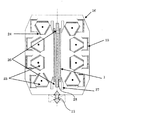
- FIG. 4 shows a configuration diagram of a sputtering chamber of a conventional sputtering apparatus as viewed from above among film forming apparatuses.
- a load lock chamber and the like for transferring or carrying a glass substrate from the atmosphere side to the sputtering chamber 16 are omitted.
- the sputtering chamber 16 for example, four triangular cathodes 23 are attached to the left and right, and a target 24 as a thin film material source is attached to each surface.
- the number of cathodes 23 can be changed according to the size of the substrate 1.
- the triangular cathodes 23 are respectively rotated and directed toward the substrate side and the back surface discharge side.
- the back surface discharge is mainly used for aging of the target rod 24, and the film of the target 24, which is a thin film material source, is attached to the shield 25 on the back surface. Since the cathode 23 has a triangular prism shape, a maximum of three types of film formation can be performed. Further, two substrates 1 can be simultaneously formed by cathodes 23 arranged on the left and right.
- FIG. 5 shows a front view of a conventional substrate tray 26 with a mask 27 attached thereto
- FIG. 6 shows a cross-sectional view taken along the line A-A ′ of FIG.
- FIG. 5 shows a state in which the substrate 1 at the opening of the substrate tray 26 is held by the side clamp 28 as a holder coming into contact with the peripheral portion (end surface) of the substrate 1.
- FIG. 6 shows a state in which the mask 27 covers the entire frame excluding the opening of the substrate tray 26 and the side clamps 28 so that the film is not attached thereto.
- a mask 27 covers the entire frame of the substrate tray 26. In this manner, the substrate tray 26 and the side clamp 28 are prevented from being coated with the film in the state shown in FIG. 5 or FIG.
- a gas such as Ar is introduced into the sputtering chamber 16.
- a predetermined voltage is applied to the cathode 23 side to perform sputtering discharge.
- the voltage and gas on the cathode 23 side are stopped, and then the mask 27 is separated from the substrate tray 26.
- the substrate tray 26 is transferred from the sputtering chamber 16 to a substrate processing chamber (not shown).
- the side clamp 28 is arranged so as to be hidden by the mask 27 during film formation, but sputtered particles, which are thin film material particles, are also present in the side clamp 28. It had adhered.
- the sputtered particles that are being sputtered contain, for example, a component in which gas molecules such as Ar collide and the sputtered particles go straight obliquely with respect to the normal of the surface to be processed of the substrate 1.
- the sputtered particles traveling straight at an angle also adhere to the side clamp 28 that should be covered by the mask 27. Therefore, the side clamp 28 with the film has conductivity, and there is a problem that dielectric breakdown occurs between the side clamp 28 and the substrate 1 made of glass, and arcing (abnormal discharge) occurs. .
- the film attached to the side clamp 28 was in contact with the substrate 1, and this caused particles that the adhered film contaminated the substrate 1. Further, when arcing or particles are generated, the electrode may be disconnected as a screen display element.
- An object of the present invention is to provide a film forming apparatus capable of reducing adhesion of thin film material particles to a holding mechanism provided in a substrate tray during film formation.
- the present invention provides a film forming apparatus, a substrate support surface for supporting a substrate, a support portion disposed around the substrate support surface, and the substrate support surface. And a holding mechanism for holding the substrate, and is configured to be detachable from the film forming apparatus, wherein the substrate support surface faces upward in the gravity direction and the gravity direction.
- a substrate tray configured to be installed in the film forming apparatus so as to be inclined from the substrate, a moving mechanism for changing the position of the holding mechanism between the film formation on the substrate and the transport of the substrate, An opening having a predetermined shape through which thin film material particles from a thin film material source facing a substrate tray installed in the film apparatus pass, and the thin film having the predetermined shape is supported on the substrate supported by the substrate support surface
- a mask for forming, the support portion When the plate tray is installed in the film forming apparatus in the inclined state, the plate tray is formed so as to be positioned on the lower side in the gravity direction of the substrate supported by the substrate supporting surface, and the mask is formed during film formation.
- the support unit, the holding mechanism, and the substrate tray are arranged to cover a part of the substrate supported by the substrate tray, and the moving mechanism holds the substrate by the holding mechanism during the transport.
- the mechanism is moved, and the holding mechanism is moved from the position where the substrate is held by the holding mechanism to the outside of the substrate tray during the transfer in the area covered by the mask during the film formation. It is characterized by.
- the clamp as the holding mechanism is in contact with the lower side of the substrate and the two corners at both ends of the side. Since holding is performed, generation of arcing can be suppressed and particles can be reduced.
- FIG. 2 is a cross-sectional view of the substrate tray when forming a thin film according to an embodiment of the present invention, and is a cross-sectional view taken along line B-B ′ of FIG. It is a side view of the lower part of a substrate tray at the time of thin film formation concerning one embodiment of the present invention.
- It is the block diagram which looked at the sputtering chamber of the conventional sputtering device from the top. It is a front view in the state where the mask was attached to the conventional substrate tray.
- FIG. 6 is a cross-sectional view taken along line A-A ′ of FIG. 5. This is a cross-sectional structure of an a-Si type TFT (Thin FilmTransistor). It is a figure which shows an example of the moving mechanism for moving the holding mechanism which concerns on one Embodiment of this invention.
- a-Si type TFT Thin FilmTransistor
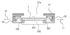
- FIG. 1 is a front view of a substrate tray when forming a thin film according to an embodiment of the present invention
- FIG. 2 is a cross-sectional view taken along line BB ′ of FIG. 1
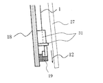
- FIG. 3 is a substrate tray when forming a thin film. The side view of the lower part of is shown.
- the substrate tray 18 includes a plurality of side clamps 19 and a bottom clamp 31 as a substrate support, and is detachable from a sputtering chamber 16 as a film forming apparatus. It is configured.
- the side clamps 19 are holding mechanisms for holding a substrate
- the plurality of side clamps 19 are regions 181 of the substrate tray 18 where the substrate 1 is disposed when the substrate tray 18 is disposed horizontally. It is arranged to surround.
- An opening 182 is formed in the region 181, and a convex portion 183 is provided on the edge of the opening 182 of the region 181 so as to surround the opening 182. With such a configuration, the substrate 1 can be placed on the convex portion 183 when the substrate tray 18 is horizontally disposed.
- the substrate tray 18 is provided with a moving mechanism (not shown in FIGS. 1 to 3) for moving the side clamp 19, and the side clamp 19 causes the substrate 1 to move on the substrate tray 18 by the moving mechanism. Move in a direction away from the located region (i.e., region 181) (i.e., toward the outside of the substrate tray 18) and toward the region (i.e., the region 181) (i.e., toward the inside of the substrate tray 18).
- the side clamp 19 is configured to be movable in the outward direction and the inward direction of the substrate tray 18, so that the substrate 1 is held by the side clamp 19 when the substrate tray 18 is transported.
- the side clamp 19 can be arranged away from the substrate 1 when forming a thin film. An example of the moving mechanism will be described later.
- the bottom clamp 31 is disposed so as to be positioned below the substrate in the gravitational direction when the substrate tray 18 is erected from a horizontally disposed state (for example, when disposed substantially vertically). That is, the substrate tray 18 is configured such that the substrate 1 is positioned on the bottom clamp 31 when the substrate tray 18 is installed in the sputtering chamber 16 as a film forming chamber as shown in FIG. As described above, the bottom clamp 31 functions as a support portion that supports the substrate 1 when the substrate tray 18 is inclined and installed (when installed in the sputtering chamber 16).
- the substrate tray 18 is configured to be able to hold the substrate 1 held on the substrate tray 18 in a standing state with a predetermined inclination in a film forming chamber such as the sputtering chamber 16. That is, the substrate tray 18 is placed in the sputtering chamber 16 in a state where the support surface for supporting the substrate 1 is inclined by a predetermined angle from the state in which the support surface is positioned parallel to the direction of gravity to the side opposite to the support surface of the substrate tray 18. It is configured so that it can be placed.
- the substrate tray 18 is configured so that the substrate support surface of the substrate tray 18 is tilted from the direction parallel to the gravity direction P so that the substrate support surface is on the upper side in the gravity direction,
- the bottom clamp 31 is provided so as to be positioned below the substrate 1 in the direction of gravity P when the substrate is tilted. Therefore, even if the substrate tray 18 is installed in the sputtering chamber 16 and the side clamp 19 does not hold the substrate 1, the substrate 1 can be held on the substrate tray 18 without falling down.
- the substrate 1 can be swung on the substrate tray 18 (in the present embodiment, the convex portion 183) by the above-described tilted arrangement, and the bottom clamp 31 is provided on the side of the substrate 1 on the gravity direction P side (lower side described later). Can be supported.
- FIG. 1 when a thin film is formed, a bottom clamp 31 that contacts a lower side of the substrate 1 and two corners at both ends of the side at a predetermined position in the sputtering chamber 16 is formed in the opening of the substrate tray 18.
- region 181) is shown. That is, when the arrow direction P in FIGS. 1 and 3 is the gravity direction, the substrate support surface of the substrate tray 18 is inclined from a state parallel to the gravity direction P, and the substrate tray 18 is installed in the sputtering chamber 16.
- the lower side of the substrate 1 refers to the lowermost side (the lowest side in the direction of gravity P) of the substrate 1 leaning against the substrate tray 18.
- the edge region of the substrate tray 18 including the side clamp 19 and the bottom clamp 31 and a predetermined region of the substrate 1 are masked, and the surface to be processed of the substrate 1 is a thin film material source.
- a mask 27 is disposed so as to be exposed to the cathode 23. That is, as shown in FIG. 2, an opening 27a having a predetermined shape is formed in the mask 27, and the sputtered particles generated from the target 24 supported by the cathode 23 are allowed to pass through the opening 27a, so that the substrate 1 A thin film having the predetermined shape can be formed thereon.
- the mask 27 is provided in the sputtering chamber 16 and has a mask drive mechanism (not shown) for changing the position of the mask 27.
- the control device controls the mask driving mechanism, so that the mask 27 can be mounted on the substrate tray 18 when the substrate tray 18 is installed in the sputtering chamber 16. That is, the mask 27 is held at a predetermined position in the sputtering chamber 16 at times other than during film formation.
- the control device controls the mask driving mechanism to move the mask 27 located at the predetermined position so that the region other than the region 181 of the substrate tray 18 is moved. (A region including the side clamp 19 and the bottom clamp 31) and a predetermined region of the substrate 1 (a portion where the substrate 1 is exposed in the shape of the opening 27a).
- the side clamp 19 when the thin film is formed, the side clamp 19 is completely covered with the mask 27 by applying the force indicated by the reference numeral 10 or 11 in FIG. Can be slid to a position that does not occur.
- 3 shows that when the thin film is formed, the side clamp 19 holding the lower side of the substrate 1 slides by applying a force of reference numeral 12, and the substrate 1 is attached to both ends of the lower side. A state in which the two attached corners are held only by the bottom clamp 31 is shown.
- the side clamp 19 is moved in the direction toward the outside of the substrate tray 18 (direction along the forces 10 and 11) by the moving mechanism, and the side clamp 19 is moved to the inner edge of the mask 27 (the center of the substrate 1). It can be arranged away from the edge of the direction to the outside of the substrate tray 18.
- the outside of the substrate tray 18 is covered with a mask 27, and the further away the substrate tray 18, the farther from the inner edge of the mask 27 (the portion where the substrate 1 is exposed with respect to the cathode 23). Therefore, when the side clamp 19 is disposed away from the inner edge of the mask 27 to the outside of the substrate tray 18 during film formation, the side portion is located in the back of the region on the substrate tray 18 covered by the mask 27.
- the clamp 19 will be arranged. Therefore, even if the sputtered particles collide with gas molecules such as Ar and the sputtered particles are incident on the substrate 1 at an angle, the amount of sputtered particles reaching the side clamp 19 can be reduced.
- the substrate 1 when the substrate 1 is transported by the substrate tray 18, the substrate 1 is supported by the side clamps 19 arranged around the region 181. Therefore, for example, when the substrate 1 is transferred to the outside of the sputtering chamber 16 after the film formation is completed, a force opposite to the forces 10 and 11 is applied to the side clamp 19. As a result, the side clamp 19 disposed outside the substrate tray 18 is moved in the direction toward the inside of the substrate tray 18, the side clamp 19 is brought into contact with the substrate 1, and the substrate 1 is moved by the side clamp 19. Hold. In this way, by changing the position of the side clamp 19 between the film formation and the substrate transfer, the region in which the side clamp 19 is covered with the mask 27 during the film formation in which the sputtered particles fly.
- the side clamp 19 can be arranged in the back of the substrate, and the substrate 1 can be firmly held (clamped) by the side clamp 19 when the substrate is transported.
- the substrate 1 is held by the side clamp 19 when the substrate is transported.
- the side clamp 19 is moved from the position holding the substrate 1 to the far side of the region covered with the mask (the substrate tray 18 by the moving mechanism).
- the side clamp 19 is moved to the outside. If the film forming operation is performed in this state, adhesion of the sputtered particles to the side clamp 19 can be reduced.
- the moving mechanism may be a mechanism that interlocks the state of the clamp when the thin film is formed with the attachment of the mask 27. That is, when the side clamp 19 holds the substrate 1, the substrate 1 can be pressed by the spring force connecting the side clamp 19 and the substrate tray 18 in conjunction with the removal of the mask 27.
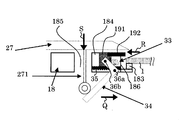
- FIG. 8 is a diagram illustrating an example of the moving mechanism, and is a diagram for explaining the moving mechanism when the attachment / detachment of the mask 27 and the movement of the side clamp 19 are interlocked.
- reference numeral 191 denotes a base part of the side clamp 19
- reference numeral 192 denotes a clamp part for clamping the substrate 1.
- the substrate tray 18 has a hollow portion 184. Further, a through hole 185 is formed in the substrate tray 18.
- the moving mechanism includes a spring 33, an L-shaped jig 34, a guide portion 35 for guiding the base portion 191, and pins 36a and 36b.
- the guide portion 35 is disposed in the hollow portion 184, and one end of the spring 33 is connected to the inner wall 186 of the hollow portion 184 and the other end is connected to the base portion 191.
- An opening is formed in the inner wall 185, and a clamp part 192 projects from the opening to the outside of the hollow part 184.
- the L-shaped jig 34 is rotatably attached to the bottom of the hollow portion 184 by a pin 36a.
- the L-shaped jig 34 is rotatably attached to the base 191 by a pin 36b.
- the L-shaped jig 34 is rotatably fixed to each of the bottom portion of the hollow portion 184 and the base portion 191 slidably disposed on the guide portion 35. Therefore, when the L-shaped jig 34 rotates in the arrow direction Q, the base 191 (side clamp 19) can be moved in the arrow direction R in conjunction with the rotation.
- the mask 27 is provided with a bar portion 271.
- the bar portion 271 passes through the through-hole 185 and moves the L-shaped jig 34 in the arrow direction S. Press on.
- the rod portion 271 on the mask 27 pushes the L-shaped jig 34 connected to the side clamp 19 as shown in FIG.
- the side clamp 19 moves away. That is, when the control device drives a mask driving mechanism (not shown) to bring the mask 27 close to the substrate tray 18 installed in the sputtering chamber 16, the rod portion 271 is inserted into the L-shaped jig 34 through the through hole 185. The L-shaped jig 34 is pressed toward the arrow direction S.
- the base 191 moves along the arrow direction R in the arrow direction R while extending the spring 33 in conjunction with the rotation. Move.
- the control device stops the movement of the mask 27 along the arrow direction S, the movement of the rod portion 271 is also stopped, and the movement of the L-shaped jig 34 and the base portion 191 is also stopped. Therefore, at the time of film formation, the base 191 and the clamp 192 can be retracted into the back of the region covered with the mask 27.
- the side clamp 19 holds the substrate 1 (for example, when the substrate 1 is transported), the rod portion 271 associated with the mask 27 is separated, and the force of the spring 33 that connects the side clamp 19 and the substrate tray 18 is separated. Hold the substrate 1. That is, when the control device controls the mask driving mechanism to move the mask 27 away from the substrate tray 18, the bar portion 271 moves in the direction opposite to the arrow direction S, and the bar portion 271 is moved from the L-shaped jig 34. The pressure on the L-shaped jig 34 is released.
- a restoring force acts on the extended spring 33, and the restoring force causes the base portion 191 to move the guide portion 35 on the side opposite to the arrow direction R.
- the base portion 191 and the clamp portion 192 that have been retracted at the time of film formation can be pulled out and the substrate 1 can be supported by the clamp portion 192.
- the substrate 1 can be held by newly attaching a convex portion 183 as a substrate receiver to the substrate tray 18 below the clamp portion 192. Since the substrate tray 18 and the substrate 1 are inclined, the substrate 1 does not fall down as described above.
- the side clamp 19 moves away from the substrate 1 during film formation, the side clamp 19 is applied with a repulsive force (pushing back force) against a spring (not shown) in conjunction with the mounting of the mask 27.
- a repulsive force pumping back force
- a spring not shown
- the side clamp 19 can be moved by an electromagnetic drive mechanism (for example, a drive mechanism such as an actuator is provided and the drive mechanism is controlled by a control device), for example, a discharge start signal or gas A mechanism that can be interlocked via an introduction signal and an electrical signal may be used.
- an electromagnetic drive mechanism for example, a drive mechanism such as an actuator is provided and the drive mechanism is controlled by a control device
- a discharge start signal or gas A mechanism that can be interlocked via an introduction signal and an electrical signal may be used.
- the movement (slide) distance of the side clamp 19 that prevents the film from being deposited by sputtering varies depending on the sputtering power, gas pressure, and the distance between the mask and the glass substrate. It is also possible to select arbitrarily according to these conditions.
- the voltage and gas on the cathode 23 side are stopped, and at the same time, the mask 27 is separated from the substrate tray 18 and the side clamp 19 holds the substrate 1 again.
- the substrate processing chamber (not shown).
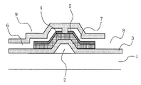
- FIG. 7 shows a cross-sectional structure of an a-Si type TFT (Thin Film Transistor).
- a film forming apparatus is used in an array manufacturing process and a BM (black matrix) manufacturing process.
- transistors and wirings are formed on the substrate 1, but the processes in which sputtering is mainly used for film formation are the following processes a, d, and e, which are sequentially stacked from a to f below.
Landscapes
- Chemical & Material Sciences (AREA)
- Mechanical Engineering (AREA)
- Chemical Kinetics & Catalysis (AREA)
- Engineering & Computer Science (AREA)
- Materials Engineering (AREA)
- Metallurgy (AREA)
- Organic Chemistry (AREA)
- Physics & Mathematics (AREA)
- Nonlinear Science (AREA)
- General Physics & Mathematics (AREA)
- Optics & Photonics (AREA)
- Crystallography & Structural Chemistry (AREA)
- Physical Vapour Deposition (AREA)
Abstract
Description
ここで、基板1の下部の辺とは、基板トレイ18に立てかけられた基板1において最下部の辺(重力方向Pの最も下側の辺)のことをいう。
実際の表示用素子の製造方法において、成膜装置が用いられるのは、アレイ製造工程とBM(ブラックマトリックス)製造工程である。例えば、アレイ製造工程では基板1上にトランジスタや配線を形成するが、成膜に関して主にスパッタリングが用いられる工程は次のa、d、eの工程であり、以下のaからfまで順次積層される。
工程a. ゲート電極 (Mo、Al等) 2
工程b. ゲート絶縁膜 (SiNx 等) 3
工程c. 半導体層 (a-Si、a-Si(n+)P等) 4、5
工程d. ソース・ドレイン電極 (Mo、Al等) 6、7
工程e. 透明電極 (ITO等) 8
工程f. 保護膜 (SiNx等) 9
Claims (4)
- 成膜装置であって、
基板を支持するための基板支持面と、該基板支持面の周囲に配置された支持部と、前記基板支持面の周囲に配置され、基板を保持するための保持機構とを有し、前記成膜装置に着脱可能に構成された基板トレイであって、前記基板支持面が重力方向上側を向いて該重力方向から傾斜するように前記成膜装置内に設置可能に構成された基板トレイと、
前記基板への成膜時と前記基板の搬送時とで前記保持機構の位置を変更させる移動機構と、
前記成膜装置内に設置された基板トレイに対向する薄膜材料源からの薄膜材料粒子が通過する所定の形状の開口を有し、該所定の形状の薄膜を前記基板支持面に支持された基板上に形成するためのマスクとを備え、
前記支持部は、前記基板トレイを前記傾斜の状態で前記成膜装置内に設置する場合に、前記基板支持面に支持される基板の重力方向下側に位置するように形成されており、
前記マスクは、成膜時において、前記支持部、前記保持機構、および前記基板トレイに支持される基板の一部を覆うように配置され、
前記移動機構は、前記搬送時には前記保持機構により前記基板を保持するように前記保持機構を移動させ、前記成膜時には前記マスクに覆われた領域において、前記搬送時において前記保持機構により前記基板を保持している位置から前記基板トレイの外側に向けて前記保持機構を移動させることを特徴とする成膜装置。 - 前記移動機構は、前記マスクの配置と、前記基板を保持している位置から前記基板トレイの外側に向けて前記保持機構を移動させる動作とを連動して行うように構成されていることを特徴とする請求項1に記載の成膜装置。
- 前記支持部は、前記基板トレイを前記傾斜の状態で前記成膜装置内に設置する場合に、前記基板支持面に支持される基板の重力方向下側の辺及び該辺の両端の2つの角部と接触することを特徴とする請求項1に記載の成膜装置。
- 請求項1に記載の成膜装置は、スパッタリング装置であることを特徴とする成膜装置。
Priority Applications (3)
| Application Number | Priority Date | Filing Date | Title |
|---|---|---|---|
| JP2011528821A JPWO2011024853A1 (ja) | 2009-08-26 | 2010-08-25 | 成膜装置 |
| CN201080037760XA CN102549190A (zh) | 2009-08-26 | 2010-08-25 | 成膜设备 |
| US13/372,660 US20120199477A1 (en) | 2009-08-26 | 2012-02-14 | Film forming apparatus |
Applications Claiming Priority (2)
| Application Number | Priority Date | Filing Date | Title |
|---|---|---|---|
| JP2009-194900 | 2009-08-26 | ||
| JP2009194900 | 2009-08-26 |
Related Child Applications (1)
| Application Number | Title | Priority Date | Filing Date |
|---|---|---|---|
| US13/372,660 Continuation US20120199477A1 (en) | 2009-08-26 | 2012-02-14 | Film forming apparatus |
Publications (1)
| Publication Number | Publication Date |
|---|---|
| WO2011024853A1 true WO2011024853A1 (ja) | 2011-03-03 |
Family
ID=43627953
Family Applications (1)
| Application Number | Title | Priority Date | Filing Date |
|---|---|---|---|
| PCT/JP2010/064371 Ceased WO2011024853A1 (ja) | 2009-08-26 | 2010-08-25 | 成膜装置 |
Country Status (5)
| Country | Link |
|---|---|
| US (1) | US20120199477A1 (ja) |
| JP (1) | JPWO2011024853A1 (ja) |
| KR (1) | KR20120043095A (ja) |
| CN (1) | CN102549190A (ja) |
| WO (1) | WO2011024853A1 (ja) |
Cited By (7)
| Publication number | Priority date | Publication date | Assignee | Title |
|---|---|---|---|---|
| US20130276978A1 (en) * | 2012-04-19 | 2013-10-24 | Intevac, Inc. | Dual-mask arrangement for solar cell fabrication |
| KR101366839B1 (ko) * | 2012-03-30 | 2014-02-26 | (주)에스엔텍 | 고온 공정용 트레이 |
| KR101366840B1 (ko) * | 2012-03-30 | 2014-02-26 | (주)에스엔텍 | 고온 공정용 트레이 |
| US9502276B2 (en) | 2012-04-26 | 2016-11-22 | Intevac, Inc. | System architecture for vacuum processing |
| US9543114B2 (en) | 2014-08-05 | 2017-01-10 | Intevac, Inc. | Implant masking and alignment system with rollers |
| US20170062258A1 (en) * | 2012-04-19 | 2017-03-02 | Intevac, Inc. | Wafer plate and mask arrangement for substrate fabrication |
| US10062600B2 (en) | 2012-04-26 | 2018-08-28 | Intevac, Inc. | System and method for bi-facial processing of substrates |
Families Citing this family (11)
| Publication number | Priority date | Publication date | Assignee | Title |
|---|---|---|---|---|
| USD689534S1 (en) * | 2010-08-30 | 2013-09-10 | Ulvac, Inc. | Film-forming apparatus |
| JP2014078601A (ja) * | 2012-10-10 | 2014-05-01 | Sumitomo Heavy Ind Ltd | 成膜装置用基板搬送トレイ、及び外部開閉駆動装置 |
| JP2014077170A (ja) * | 2012-10-10 | 2014-05-01 | Sumitomo Heavy Ind Ltd | 成膜装置 |
| JP2014177683A (ja) * | 2013-03-15 | 2014-09-25 | Sumitomo Heavy Ind Ltd | 基板搬送トレイ、及び成膜装置 |
| KR102219198B1 (ko) * | 2013-08-02 | 2021-02-22 | 어플라이드 머티어리얼스, 인코포레이티드 | 기판들을 위한 유지 배열, 및 이를 사용하는 장치 및 방법 |
| KR102190806B1 (ko) * | 2013-08-02 | 2020-12-14 | 어플라이드 머티어리얼스, 인코포레이티드 | 기판들을 위한 유지 배열, 및 이를 사용하기 위한 장치 및 방법 |
| JP6484786B2 (ja) | 2014-12-03 | 2019-03-20 | 株式会社Joled | 表示装置および表示装置の製造方法、並びに電子機器 |
| KR101554840B1 (ko) * | 2015-01-27 | 2015-09-21 | 엘피티 주식회사 | 탄성 박판을 이용한 필름부착기용 파렛트식 공정대응유닛 |
| US10468221B2 (en) * | 2017-09-27 | 2019-11-05 | Applied Materials, Inc. | Shadow frame with sides having a varied profile for improved deposition uniformity |
| CN111020517B (zh) * | 2019-12-02 | 2021-11-23 | Tcl华星光电技术有限公司 | 一种基板承托架 |
| JP7287356B2 (ja) * | 2020-07-03 | 2023-06-06 | 株式会社村田製作所 | 成膜用マスク治具および成膜装置 |
Citations (3)
| Publication number | Priority date | Publication date | Assignee | Title |
|---|---|---|---|---|
| JP2003147519A (ja) * | 2001-11-05 | 2003-05-21 | Anelva Corp | スパッタリング装置 |
| WO2006054663A1 (ja) * | 2004-11-22 | 2006-05-26 | Sharp Kabushiki Kaisha | 基板保持装置および基板処理装置ならびに液晶表示装置 |
| JP2008202146A (ja) * | 2008-04-21 | 2008-09-04 | Ulvac Japan Ltd | 縦型化学気相成長装置及び該装置を用いた成膜方法 |
Family Cites Families (3)
| Publication number | Priority date | Publication date | Assignee | Title |
|---|---|---|---|---|
| US4558388A (en) * | 1983-11-02 | 1985-12-10 | Varian Associates, Inc. | Substrate and substrate holder |
| DE4305750C2 (de) * | 1993-02-25 | 2002-03-21 | Unaxis Deutschland Holding | Vorrichtung zum Halten von flachen, kreisscheibenförmigen Substraten in der Vakuumkammer einer Beschichtungs- oder Ätzanlage |
| JP3695971B2 (ja) * | 1998-12-22 | 2005-09-14 | シャープ株式会社 | 成膜装置および成膜方法 |
-
2010
- 2010-08-25 WO PCT/JP2010/064371 patent/WO2011024853A1/ja not_active Ceased
- 2010-08-25 CN CN201080037760XA patent/CN102549190A/zh active Pending
- 2010-08-25 JP JP2011528821A patent/JPWO2011024853A1/ja not_active Withdrawn
- 2010-08-25 KR KR1020127006402A patent/KR20120043095A/ko not_active Ceased
-
2012
- 2012-02-14 US US13/372,660 patent/US20120199477A1/en not_active Abandoned
Patent Citations (3)
| Publication number | Priority date | Publication date | Assignee | Title |
|---|---|---|---|---|
| JP2003147519A (ja) * | 2001-11-05 | 2003-05-21 | Anelva Corp | スパッタリング装置 |
| WO2006054663A1 (ja) * | 2004-11-22 | 2006-05-26 | Sharp Kabushiki Kaisha | 基板保持装置および基板処理装置ならびに液晶表示装置 |
| JP2008202146A (ja) * | 2008-04-21 | 2008-09-04 | Ulvac Japan Ltd | 縦型化学気相成長装置及び該装置を用いた成膜方法 |
Cited By (9)
| Publication number | Priority date | Publication date | Assignee | Title |
|---|---|---|---|---|
| KR101366839B1 (ko) * | 2012-03-30 | 2014-02-26 | (주)에스엔텍 | 고온 공정용 트레이 |
| KR101366840B1 (ko) * | 2012-03-30 | 2014-02-26 | (주)에스엔텍 | 고온 공정용 트레이 |
| US20130276978A1 (en) * | 2012-04-19 | 2013-10-24 | Intevac, Inc. | Dual-mask arrangement for solar cell fabrication |
| US9525099B2 (en) * | 2012-04-19 | 2016-12-20 | Intevac, Inc. | Dual-mask arrangement for solar cell fabrication |
| US20170062258A1 (en) * | 2012-04-19 | 2017-03-02 | Intevac, Inc. | Wafer plate and mask arrangement for substrate fabrication |
| US10679883B2 (en) * | 2012-04-19 | 2020-06-09 | Intevac, Inc. | Wafer plate and mask arrangement for substrate fabrication |
| US9502276B2 (en) | 2012-04-26 | 2016-11-22 | Intevac, Inc. | System architecture for vacuum processing |
| US10062600B2 (en) | 2012-04-26 | 2018-08-28 | Intevac, Inc. | System and method for bi-facial processing of substrates |
| US9543114B2 (en) | 2014-08-05 | 2017-01-10 | Intevac, Inc. | Implant masking and alignment system with rollers |
Also Published As
| Publication number | Publication date |
|---|---|
| US20120199477A1 (en) | 2012-08-09 |
| CN102549190A (zh) | 2012-07-04 |
| JPWO2011024853A1 (ja) | 2013-01-31 |
| KR20120043095A (ko) | 2012-05-03 |
Similar Documents
| Publication | Publication Date | Title |
|---|---|---|
| WO2011024853A1 (ja) | 成膜装置 | |
| JP4856308B2 (ja) | 基板処理装置及び経由チャンバー | |
| US7407358B2 (en) | Interback-type substrate processing device | |
| JP6936205B2 (ja) | 成膜装置及びこれを用いる有機el表示装置の製造方法 | |
| KR102245762B1 (ko) | 홀더, 홀더를 갖는 캐리어, 및 기판을 고정시키기 위한 방법 | |
| US20110053301A1 (en) | Thin film deposition apparatus and method of manufacturing organic light-emitting display device by using the same | |
| JP7278193B2 (ja) | 成膜装置 | |
| TW201518532A (zh) | 用於基板之支承配置及應用其之設備及方法 | |
| KR20210053761A (ko) | 성막 장치 및 성막 방법 | |
| JP4612516B2 (ja) | スパッタ装置およびスパッタ装置用キャリア | |
| JP5035499B2 (ja) | スパッタ装置および基板搬送用キャリア | |
| CN101225505B (zh) | 基板保持台和使用其的成膜方法、成膜装置 | |
| JP2011099162A (ja) | 薄膜形成装置、薄膜の製造方法及び電子素子の製造方法 | |
| US20070138009A1 (en) | Sputtering apparatus | |
| CN112779504B (zh) | 成膜装置及成膜方法 | |
| JP2006089793A (ja) | 成膜装置 | |
| JP4739445B2 (ja) | 基板処理装置 | |
| KR100714882B1 (ko) | 평면디스플레이용 화학 기상 증착장치 | |
| KR20090058993A (ko) | 마그네트론 스퍼터링장치 및 구동방법 | |
| KR101032438B1 (ko) | 액정표시패널의 제조장치 | |
| CN101469403B (zh) | 等离子体显示屏的基板保持件 | |
| WO2019228610A1 (en) | Holder, carrier comprising at least two holders, apparatuses and methods | |
| JP5467894B2 (ja) | 基板処理装置及び表示用素子の製造方法 | |
| JP2009149945A (ja) | インラインスパッタ装置 | |
| KR20250081914A (ko) | 기판을 위한 마스크, 기판 지지부, 기판 처리 장치, 기판 상의 층 증착을 위한 방법, 및 하나 이상의 디바이스를 제조하는 방법 |
Legal Events
| Date | Code | Title | Description |
|---|---|---|---|
| WWE | Wipo information: entry into national phase |
Ref document number: 201080037760.X Country of ref document: CN |
|
| 121 | Ep: the epo has been informed by wipo that ep was designated in this application |
Ref document number: 10811902 Country of ref document: EP Kind code of ref document: A1 |
|
| WWE | Wipo information: entry into national phase |
Ref document number: 2011528821 Country of ref document: JP |
|
| NENP | Non-entry into the national phase |
Ref country code: DE |
|
| ENP | Entry into the national phase |
Ref document number: 20127006402 Country of ref document: KR Kind code of ref document: A |
|
| 122 | Ep: pct application non-entry in european phase |
Ref document number: 10811902 Country of ref document: EP Kind code of ref document: A1 |