WO2011024754A1 - Iii族窒化物半導体積層ウェハ及びiii族窒化物半導体デバイス - Google Patents
Iii族窒化物半導体積層ウェハ及びiii族窒化物半導体デバイス Download PDFInfo
- Publication number
- WO2011024754A1 WO2011024754A1 PCT/JP2010/064174 JP2010064174W WO2011024754A1 WO 2011024754 A1 WO2011024754 A1 WO 2011024754A1 JP 2010064174 W JP2010064174 W JP 2010064174W WO 2011024754 A1 WO2011024754 A1 WO 2011024754A1
- Authority
- WO
- WIPO (PCT)
- Prior art keywords
- layer
- group iii
- iii nitride
- nitride semiconductor
- aln
- Prior art date
- Legal status (The legal status is an assumption and is not a legal conclusion. Google has not performed a legal analysis and makes no representation as to the accuracy of the status listed.)
- Ceased
Links
Images






Classifications
-
- H—ELECTRICITY
- H10—SEMICONDUCTOR DEVICES; ELECTRIC SOLID-STATE DEVICES NOT OTHERWISE PROVIDED FOR
- H10D—INORGANIC ELECTRIC SEMICONDUCTOR DEVICES
- H10D30/00—Field-effect transistors [FET]
- H10D30/40—FETs having zero-dimensional [0D], one-dimensional [1D] or two-dimensional [2D] charge carrier gas channels
- H10D30/47—FETs having zero-dimensional [0D], one-dimensional [1D] or two-dimensional [2D] charge carrier gas channels having two-dimensional [2D] charge carrier gas channels, e.g. nanoribbon FETs or high electron mobility transistors [HEMT]
- H10D30/471—High electron mobility transistors [HEMT] or high hole mobility transistors [HHMT]
- H10D30/473—High electron mobility transistors [HEMT] or high hole mobility transistors [HHMT] having confinement of carriers by multiple heterojunctions, e.g. quantum well HEMT
- H10D30/4732—High electron mobility transistors [HEMT] or high hole mobility transistors [HHMT] having confinement of carriers by multiple heterojunctions, e.g. quantum well HEMT using Group III-V semiconductor material
- H10D30/4738—High electron mobility transistors [HEMT] or high hole mobility transistors [HHMT] having confinement of carriers by multiple heterojunctions, e.g. quantum well HEMT using Group III-V semiconductor material having multiple donor layers
-
- H—ELECTRICITY
- H10—SEMICONDUCTOR DEVICES; ELECTRIC SOLID-STATE DEVICES NOT OTHERWISE PROVIDED FOR
- H10D—INORGANIC ELECTRIC SEMICONDUCTOR DEVICES
- H10D62/00—Semiconductor bodies, or regions thereof, of devices having potential barriers
- H10D62/80—Semiconductor bodies, or regions thereof, of devices having potential barriers characterised by the materials
- H10D62/85—Semiconductor bodies, or regions thereof, of devices having potential barriers characterised by the materials being Group III-V materials, e.g. GaAs
- H10D62/8503—Nitride Group III-V materials, e.g. AlN or GaN
Definitions
- the present invention relates to a group III nitride semiconductor laminated wafer and a group III nitride semiconductor device.
- Non-Patent Document 1 describes a heterojunction transistor (HFET: Heterojunction Field-Effect Transistor).
- HFET Heterojunction Field-Effect Transistor
- This HFET is formed on an m-plane GaN substrate.
- an undoped GaN layer (1 ⁇ m) an Fe-doped GaN layer (1.5 ⁇ m), an undoped GaN layer (300 nm) as a channel layer, and an AlGaN layer (undoped AlGaN layer as a barrier layer) on an m-plane GaN substrate (2 nm), Si-doped AlGaN layer (15 nm) and undoped AlGaN layer (6 nm)) are stacked in this order to realize an enhancement type (normally-off type) HFET.
- an enhancement type normally-off type
- Non-Patent Document 2 describes a high electron mobility transistor (HEMT: High Electron Mobility Transistor).
- HEMT High Electron Mobility Transistor
- Non-Patent Document 3 as a method for growing a GaN crystal on a SiC substrate, a method for growing GaN crystal after growing AlN on the SiC substrate, and a method for growing GaN crystal after growing AlN and AlGaN on the SiC substrate. And a method for growing them.
- Non-Patent Document 1 a channel layer and a barrier layer made of a group III nitride semiconductor are generally grown on a GaN substrate.
- a group III nitride semiconductor containing Al such as AlN
- Non-Patent Document 2 an AlN buffer layer, an AlGaN channel layer, and an AlGaN barrier layer are grown in the c-axis direction. In this case, even when the operation is stopped, a high-concentration two-dimensional electron gas is generated in the AlGaN channel layer by the piezoelectric field. Therefore, it becomes difficult to realize a normally-off type semiconductor device.
- Non-Patent Document 2 and Non-Patent Document 3 a group III nitride semiconductor layer containing Al is grown on a substrate different from the group III nitride, for example, a SiC substrate. In this case, it becomes difficult to suppress the occurrence of crystal defects in the semiconductor layer.
- the present invention has been made in view of the above problems, and an object of the present invention is to provide a normally-off group III nitride semiconductor device having a high breakdown electric field strength and few crystal defects. It is another object of the present invention to provide a group III nitride semiconductor laminated wafer used for manufacturing the group III nitride semiconductor device.
- a group III nitride semiconductor laminated wafer includes: (a) a substrate made of AlN and having a main surface along the c-axis of the AlN crystal; and (b) a group III nitride semiconductor containing Al. A first semiconductor layer formed on the main surface, and (c) a group III nitride-based semiconductor provided on the main surface and having a band gap larger than that of the first semiconductor layer. And a second semiconductor layer forming a heterojunction.
- a group III nitride semiconductor device includes: (a) a substrate made of AlN and having a main surface along the c-axis of the AlN crystal; and (b) a group III nitride semiconductor containing Al. A channel layer provided on the main surface; and (c) a group III nitride semiconductor provided on the main surface and having a band gap larger than that of the first semiconductor layer, and forming a heterojunction with the channel layer. And a barrier layer.
- an AlN substrate having a higher breakdown electric field strength than a GaN substrate is used as the substrate.
- This AlN substrate has a main surface along the c-axis. This main surface is a nonpolar surface, for example, m-plane or a-plane.
- a channel layer and a first semiconductor layer made of a group III nitride-based semiconductor containing Al are formed on the main surface. Since the piezo electric field is reduced by forming the channel layer and the first semiconductor layer on the nonpolar surface in this way, generation of two-dimensional electron gas due to the piezo electric field is generated in the channel layer and the first semiconductor layer. Can be suppressed.
- a normally-off type semiconductor device can be suitably realized.
- the first semiconductor layer and the second semiconductor layer made of a group III nitride semiconductor are formed on the AlN substrate which is a group III nitride, it is preferable to generate crystal defects in these semiconductor layers. Can be suppressed. Or since the channel layer and barrier layer which consist of a group III nitride semiconductor are formed on the AlN substrate which is a group III nitride, generation
- the normally-off type semiconductor device having a large breakdown electric field strength and few crystal defects, and the manufacturing of the semiconductor device are used.
- Laminated wafers can be provided.
- the half width of the X-ray rocking curve in the c-axis direction of the group III nitride semiconductor containing Al in the first semiconductor layer is perpendicular to the c axis of the group III nitride semiconductor.
- the X-ray rocking curve half-width of the X direction can be 1.2 times or less.
- the half width of the X-ray rocking curve in the c-axis direction of the group III nitride semiconductor containing Al in the channel layer is perpendicular to the c axis of the group III nitride semiconductor.
- the X-ray rocking curve can have a half-width of 1.2 times or less.
- the main surface can be an m-plane or a-plane of AlN crystal.
- the main surface can be the m-plane or a-plane of AlN crystal. Since the AlN substrate has these nonpolar surfaces as main surfaces, the piezoelectric field generated in the channel layer and the first semiconductor layer can be effectively reduced.
- the thickness of the first semiconductor layer can be 50 nm or less.
- the thickness of the channel layer can be 50 nm or less.
- the first semiconductor layer can be made of AlGaN.
- the channel layer can be made of AlGaN.
- the second semiconductor layer can be made of AlN.
- the first barrier layer can be made of AlN.
- the group III nitride semiconductor laminated wafer can further include a third semiconductor layer.
- the third semiconductor layer is provided on the main surface at a position where the first semiconductor layer is sandwiched between the second semiconductor layer and a group III nitride semiconductor having a larger band gap than the first semiconductor layer. And a heterojunction with the first semiconductor layer.
- the group III nitride semiconductor device may further include a second barrier layer.
- the second barrier layer is provided on the main surface at a position sandwiching the channel layer with the first barrier layer, and is made of a group III nitride semiconductor having a band gap larger than that of the channel layer, and is heterojunction with the channel layer. Is made. Thereby, a so-called double hetero structure transistor can be suitably realized.
- the third semiconductor layer can be made of AlN.
- the second barrier layer can be made of AlN.
- a normally-off group III nitride semiconductor device having a high breakdown electric field strength and few crystal defects is provided.
- a group III nitride semiconductor laminated wafer used for manufacturing the group III nitride semiconductor device is provided.
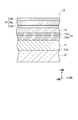
- FIG. 1 is a drawing showing the structure of a group III nitride semiconductor laminated wafer according to the first embodiment.
- FIG. 2 is a drawing showing the structure of a group III nitride semiconductor laminated wafer according to the second embodiment.
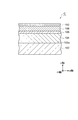
- FIG. 3 is a drawing showing the structure of a group III nitride semiconductor laminated wafer according to the third embodiment.
- FIG. 4 is a drawing showing the structure of a group III nitride semiconductor laminated wafer C as a comparative example.
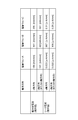
- FIG. 5 is a chart showing the evaluation results in Example 1.
- FIG. 6 is a diagram illustrating the arrangement of the source electrode S, the gate electrode G, and the drain electrode D in the second embodiment.
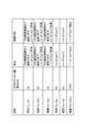
- FIG. 7 is a chart showing the evaluation results in Example 2.
- FIG. 8 is a chart showing the results in Example 3.
- FIG. 9 is a chart showing the results in Example 4.
- FIG. 10 is a drawing showing a structure of a group III nitride semiconductor device according to the fourth embodiment.
- FIG. 11 is a drawing showing a structure of a group III nitride semiconductor device according to the fifth embodiment.
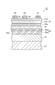
- FIG. 1 is a drawing showing a structure of a group III nitride semiconductor laminated wafer according to a first embodiment of the present invention.
- the group III nitride semiconductor laminated wafer 10 of this embodiment includes an AlN substrate 27.
- the AlN substrate 27 has a main surface 27a along the c-axis of the AlN crystal.
- FIG. 1 illustrates the c-axis direction and the m-axis direction of the AlN substrate 27, respectively.
- the main surface 27a of the AlN substrate 27 is composed of an m-plane of AlN crystal.
- the group III nitride semiconductor laminated wafer 10 includes a first Al X1 In Y1 Ga 1-X1-Y1 N (0 ⁇ X1 ⁇ 1, as a first semiconductor layer made of a group III nitride semiconductor containing Al. 0 ⁇ Y1 ⁇ 1, 0 ⁇ X1 + Y1 ⁇ 1) layer 13 and a second Al X2 In Y2Ga1 -X2-Y2N (0 ⁇ X2 ⁇ 1) as a second semiconductor layer made of a group III nitride semiconductor , 0 ⁇ Y2 ⁇ 1, 0 ⁇ X2 + Y2 ⁇ 1) layer 15.
- the second Al X2 In Y2 Ga 1-X2-Y2 N layer 15 is provided on the main surface 27a of the AlN substrate 27, and the first Al X1 In Y1 Ga 1-X1-Y1 N layer 13 is the second layer.
- the Al X2 In Y2 Ga 1-X2-Y2 N layer 15 is provided.
- the second Al X2 In Y2 Ga 1-X2-Y2 N layer 15 has a larger band gap than the first Al X1 In Y1 Ga 1-X1-Y1 N layer 13, and the first Al X1 In Y1 Ga 1- A heterojunction is formed with the X1-Y1 N layer 13.
- the first Al X1 In Y1 Ga 1-X1-Y1 N layer 13 functions as a channel layer, for example, and the second Al X2 In Y2 Ga 1-X2
- the -Y2 N layer 15 functions as a barrier layer, for example.
- the second Al X2 In Y2 Ga 1-X2 -Y2 N layer 15 includes an undoped layer 15a of the first Al X1 In Y1 Ga 1-X1 -Y1 N layer 13 close, and a doped layer 15b.
- Si is doped in the doped layer 15b.
- the first Al X1 In Y1 Ga 1-X1-Y1 N layer 13 and the second Al X2 In Y2 Ga 1-X2-Y2 N layer 15 are grown by, for example, metal organic chemical vapor deposition (MOVPE).
- MOVPE metal organic chemical vapor deposition
- the thickness of the first Al X1 In Y1 Ga 1-X1-Y1 N layer 13 is, for example, 30 nm, the Al atom composition ratio X1 is 0.8, and the In atom composition ratio Y1 is 0. It is.
- the thickness of the second Al X2 In Y2 Ga 1-X2-Y2 N layer 15 is, for example, 23 nm (of which the undoped layer 15a is 3 nm and the doped layer 15b is 20 nm), and the dopant concentration of the doped layer 15b is 1 ⁇ 10 19 cm ⁇ 3 .
- the second Al X2 In Y2 Ga 1-X2-Y2 N layer 15 is provided on the epitaxial layer 17 as a buffer layer.
- the epitaxial layer 17 is made of an undoped group III nitride semiconductor, for example, undoped AlN.
- the epitaxial layer 17 is provided on the main surface 27 a of the AlN substrate 27.
- a suitable thickness of the epitaxial layer 17 is, for example, 2 ⁇ m.
- the epitaxial layer 17 is grown by, for example, a metal organic chemical vapor deposition method.
- the manufacturing method of the group III nitride semiconductor laminated wafer 10 of this embodiment is as follows. First, an AlN substrate 27 having a main surface (preferably m-plane or a-plane) 27a along the c-axis is set in a MOVPE furnace, and in-furnace heat treatment is performed at 1150 ° C. in an NH 3 atmosphere. Next, using the MOVPE method, the epitaxial layer 17, the doped layer 15b and the undoped layer 15a of the second Al X2 In Y2 Ga 1-X2-Y2 N layer 15, and the first Al X1 In Y1 Ga 1-X1 -Y1 N layer 13 is grown sequentially.
- the AlN substrate 27 used at this time preferably has extremely excellent crystallinity such that the dislocation density of the main surface 27a is less than 1 ⁇ 10 6 cm ⁇ 2 .
- an AlN substrate 27 having a higher breakdown electric field strength than a GaN substrate is used as the substrate.
- the main surface 27a of the AlN substrate 27 is composed of an m-plane of AlN crystal, and a first Al X1 In Y1 Ga 1-X1-Y1 N layer 13 is formed on the main surface 27a.
- the generation of a two-dimensional electron gas due to the piezoelectric field can be suppressed. Therefore, a normally-off type semiconductor device can be suitably realized.
- the AlN substrate 27 which is a group III nitride
- a first Al X1 In Y1 Ga 1-X1-Y1 N layer 13 and a second Al X2 In Y2 Ga 1-X2 made of a group III nitride semiconductor are used. Since the -Y2 N layer 15 is formed, the generation of crystal defects in these semiconductor layers can be suitably suppressed.
- the main surface 27a of the AlN substrate 27 is an m-plane
- the main surface 27a only needs to be along the c-axis of the AlN crystal, and may be another nonpolar surface such as an a-plane. Even if it exists, the said effect of this embodiment can be acquired.
- FIG. 2 is a drawing showing a structure of a group III nitride semiconductor laminated wafer according to a second embodiment of the present invention.
- the group III nitride semiconductor laminated wafer 11 of the present embodiment includes a first Al X1 In Y1 Ga 1-X1-Y1 N layer 13, a second Al X2 In Y2 Ga 1-X2-Y2 N layer 15, an epitaxial layer. 17 and an AlN substrate 27. These configurations are the same as those in the first embodiment described above.
- the group III nitride semiconductor laminated wafer 11 further includes a third Al X3 In Y3 Ga 1-X3-Y3 N (0 ⁇ X3 ⁇ 1, 0 ⁇ Y3 ⁇ 1, 0 ⁇ X3 + Y3 ⁇ 1) layer 19. .
- the third Al X3 In Y3 Ga 1-X3-Y3 N layer 19 is located between the second Al X2 In Y2 Ga 1-X2-Y2 N layer 15 and the first Al X1 In Y1 Ga 1-X1- It is provided at a position sandwiching the Y1 N layer 13, and in this embodiment, it is provided on the first Al X1 In Y1 Ga 1-X1-Y1 N layer 13.
- the third Al X3 In Y3 Ga 1-X3-Y3 N layer 19 has a larger band gap than the first Al X1 In Y1 Ga 1-X1-Y1 N layer 13, and the first Al X1 In Y1 Ga 1- A heterojunction is formed with the X1-Y1 N layer 13.
- the first Al X1 In Y1 Ga 1-X1-Y1 N layer 13 functions as a channel layer, for example, and the second Al X2 In Y2 Ga 1-X2
- the -Y2 N layer 15 functions as a first barrier layer, for example, and the third Al X3 In Y3 Ga 1 -X3 -Y3 N layer 19 functions as a second barrier layer, for example.
- the third Al X3 In Y3 Ga 1-X3-Y3 N layer 19 includes an undoped layer 19a near the first Al X1 In Y1 Ga 1-X1-Y1 N layer 13, and the first Al X1 In Y1 Ga 1 -X1-Y1 includes an undoped layer 19b away from the N layer 13 and a doped layer 19c provided between the undoped layers 19a and 19b.
- Si is doped in the doped layer 19c.
- the first Al X1 In Y1 Ga 1-X1-Y1 N layer 13 can be made of AlGaN
- the second Al X2 In Y2 Ga 1-X2-Y2 N layer 15 is made of AlN. be able to.
- the third Al X3 In Y3 Ga 1-X3-Y3 N layer 19 can be made of AlN.
- the third Al X3 In Y3 Ga 1-X1-Y3 N layer 19 is grown by, for example, a metal organic chemical vapor deposition method.
- the thickness of the third Al X3 In Y3 Ga 1-X3-Y3 N layer 19 is, for example, 26 nm, and in one example, the undoped layers 15a and 15b are each 3 nm and the doped layer 19c is 20 nm. .
- the dopant concentration of the doped layer 19c is, for example, 1 ⁇ 10 19 cm ⁇ 3 .
- the manufacturing method of the group III nitride semiconductor laminated wafer 11 of this embodiment is the same as that of 1st Embodiment except for the following point. That is, after the first Al X1 In Y1 Ga 1-X1-Y1 N layer 13 is grown, the undoped layer 19a and the doped layer 19c of the third Al X3 In Y3 Ga 1-X3-Y3 N layer 19 are subsequently continued.
- the undoped layer 19b is grown by the MOVPE method.
- the AlN substrate 27 is preferably excellent in crystallinity such that the dislocation density of the main surface 27a is less than 1 ⁇ 10 6 cm ⁇ 2 .
- the group III nitride semiconductor laminated wafer 11 of this embodiment includes an AlN substrate 27, a first Al X1 In Y1 Ga 1-X1-Y1 N layer 13 and a second Al X2 In Y2 Ga similar to those in the first embodiment. Since the 1-X2-Y2 N layer 15 is provided, a normally-off type semiconductor device having a high breakdown electric field strength and few crystal defects can be manufactured.
- the group III nitride semiconductor laminated wafer 11 of the present embodiment includes a third Al X3 In Y3 Ga 1-X3-Y3 N layer 19.
- the third Al X3 In Y3 Ga 1-X3-Y3 N layer 19 is placed between the second Al X2 In Y2 Ga 1-X2-Y2 N layer 15 and the first Al X1 In Y1 Ga 1-X1.
- the band gap is larger than that of the first Al X1 In Y1 Ga 1-X1-Y1 N layer 13 and the first Al X1 In Y1 Ga 1-X1-Y1 N layer 13 And form a heterojunction.
- a so-called double heterostructure transistor can be preferably manufactured.
- FIG. 3 is a drawing showing a structure of a group III nitride semiconductor laminated wafer according to a third embodiment of the present invention.
- the group III nitride semiconductor laminated wafer 12 of the present embodiment has a first Al X1 In Y1 Ga 1-X1-Y1 N (0 ⁇ X1 ⁇ 1) as a first semiconductor layer made of a group III nitride semiconductor containing Al.
- the first Al X1 In Y1 Ga 1-X1-Y1 N layer 21 is provided directly on the main surface 27a of the AlN substrate 27, and the second Al X2 In Y2 Ga 1-X2-Y2 N layer 23 is The first Al X1 In Y1 Ga 1-X1-Y1 N layer 21 is provided.
- the second Al X2 In Y2 Ga 1-X2-Y2 N layer 23 has a larger band gap than the first Al X1 In Y1 Ga 1-X1-Y1 N layer 21, and the first Al X1 In Y1 Ga 1- A heterojunction is formed with the X1-Y1 N layer 21.
- the first Al X1 In Y1 Ga 1-X1-Y1 N layer 21 functions as a channel layer, for example, and the second Al X2 In Y2 Ga 1-X2
- the -Y2 N layer 23 functions as a barrier layer, for example.
- the second Al X2 In Y2 Ga 1-X2-Y2 N layer 23 includes an undoped layer 23a near the first Al X1 In Y1 Ga 1-X1-Y1 N layer 21, and the first Al X1 In Y1 Ga 1 -X1-Y1 includes an undoped layer 23b separated from the N layer 21 and a doped layer 23c provided between the undoped layers 23a and 23b.
- Si is doped in the doped layer 23c.
- the first Al X1 In Y1 Ga 1-X1-Y1 N layer 21 and the second Al X2 In Y2 Ga 1-X2-Y2 N layer 23 are grown by, for example, metal organic chemical vapor deposition (MOVPE).
- MOVPE metal organic chemical vapor deposition
- the thickness of the first Al X1 In Y1 Ga 1-X1-Y1 N layer 21 is, for example, 2 ⁇ m, the Al atom composition ratio X1 is 0.8, and the In atom composition ratio Y1 is 0. It is.
- the thickness of the second Al X2 In Y2 Ga 1-X2-Y2 N layer 23 is, for example, 36 nm.
- the undoped layers 23 a and 23 b are 3 nm and the doped layer 23 c is 30 nm, respectively.
- the dopant concentration of the doped layer 23c is, for example, 1 ⁇ 10 19 cm ⁇ 3 .
- the manufacturing method of the group III nitride semiconductor laminated wafer 12 of this embodiment is as follows. First, the AlN substrate 27 is heat-treated in the furnace at 1150 ° C. in an NH 3 atmosphere. Next, using the MOVPE method, the first Al X1 In Y1 Ga 1-X1-Y1 N layer 21 and the second Al X2 In Y2 Ga 1-X2-Y2 N layer 23 undoped layer 23a, doped layer 23c and the undoped layer 23b are sequentially grown. Also in this embodiment, the AlN substrate 27 is preferably excellent in crystallinity such that the dislocation density of the main surface 27a is less than 1 ⁇ 10 6 cm ⁇ 2 .
- Example 1 Here, the group III nitride semiconductor laminated wafer 10 (see FIG. 1) of the first embodiment and the group III nitride semiconductor laminated wafer 12 (see FIG. 3) of the third embodiment are produced, and the crystallinity is evaluated. The result of having performed will be described.
- AlN substrates having a main surface of m-plane and a dislocation density of the main surface of less than 1 ⁇ 10 6 cm ⁇ 2 were prepared.
- One AlN substrate includes an undoped AlN layer having a thickness of 2 ⁇ m corresponding to the epitaxial layer 17, a Si-doped AlN layer having a thickness of 20 nm corresponding to the doped layer 15 b and a dopant concentration of 1 ⁇ 10 19 cm ⁇ 3 , an undoped layer.
- An undoped AlN layer having a thickness of 3 nm corresponding to 15a and an undoped Al 0.8 Ga 0.2 N layer having a thickness of 30 nm corresponding to the first Al X1 In Y1 Ga 1-X1-Y1 N layer 13 are grown in this order. It was. Hereinafter, this is referred to as a laminated wafer A.
- the other AlN substrate corresponds to an undoped Al 0.8 Ga 0.2 N layer having a thickness of 2 ⁇ m corresponding to the first Al X1 In Y1 Ga 1-X1-Y1 N layer 21, and an undoped layer 23a.
- An undoped AlN layer having a thickness of 3 nm, an undoped AlN layer having a thickness of 30 nm corresponding to the doped layer 23c, and an undoped AlN layer having a thickness of 3 nm corresponding to the undoped layer 23b were grown in this order.
- this is referred to as a laminated wafer B.
- a group III nitride semiconductor laminated wafer C shown in FIG. 4 was produced.
- a group III nitride semiconductor laminated wafer C shown in FIG. 4 includes an AlN substrate 102 having a c-plane of AlN crystal as a main surface 102a, and an undoped Al 0.8 Ga having a thickness of 2 ⁇ m is formed on the main surface 102a.
- a 0.2 N layer 104, an undoped AlN layer 106 having a thickness of 3 nm, a Si-doped AlN layer 108 having a thickness of 30 nm and a dopant concentration of 1 ⁇ 10 19 cm ⁇ 3 , and an undoped AlN layer 110 having a thickness of 3 nm are stacked.
- the AlN substrate 102 is extremely excellent in crystallinity with a dislocation density on the main surface of less than 1 ⁇ 10 6 cm ⁇ 2 .
- FIG. 5 is a chart showing the evaluation results in this example.
- FIG. 5 shows the observation results of stacking faults and dislocations using a transmission electron microscope (TEM) for each of the above-described stacked wafers A to C.
- FIG. 5 also shows tilts in the a-axis direction and the c-axis direction on the surface of the channel layer (that is, the undoped Al 0.8 Ga 0.2 N layer) and the surface of the AlN substrate for each of the laminated wafers A to C.
- the X-ray rocking curve (XRC) half-width value corresponding to the fluctuation is shown.
- the laminated wafer C the value of the XRC half width corresponding to the tilt in the m-axis direction is shown.
- the stacking fault density is 1 ⁇ 10 6 cm ⁇ 1 or more and the dislocation density is 1 ⁇ 10 10 cm ⁇ . 1 or more.
- Stacking faults and dislocations have occurred.
- the undoped Al 0.8 Ga 0.2 N layer is stacked thick (2 ⁇ m) on the AlN substrate, so that the crystal fluctuation in the c-axis direction is larger than that in the direction perpendicular to the c-axis direction. This is probably because the stacking faults extend mainly in the direction orthogonal to the c-axis direction.
- the XRC half-value width of the channel layer (undoped Al 0.8 Ga 0.2 N layer) is larger than the XRC half-value width of the AlN substrate, and the c-axis direction is larger than the XRC half-value width of the channel layer in the a-axis direction.
- the XRC full width at half maximum is significantly large, and anisotropy occurs in the tilt of the crystal, in other words, fluctuation.
- the lamination defects and dislocations could not be confirmed from the TEM observation. From this TEM observation, the stacking fault density is less than 2 ⁇ 10 3 cm ⁇ 1 and the dislocation density is less than 1 ⁇ 10 8 cm ⁇ 1 . No stacking faults or dislocations occurred, and the XRC half-value width of the channel layer (undoped Al 0.8 Ga 0.2 N layer) was almost the same value as the AlN substrate. Anisotropy is not observed. This is probably because the laminated wafer A has a channel layer (undoped Al 0.8 Ga 0.2 N layer) formed thinner (30 nm) than the laminated wafer B.
- the channel layer is formed thin.
- the channel layer is formed thin.
- the lower limit of the thickness of the channel layer is, for example, 2 nm.
- dislocations having a dislocation density of 1 ⁇ 10 9 cm ⁇ 1 occurred in the channel layer (undoped Al 0.8 Ga 0.2 N layer), but no stacking fault could be confirmed from cross-sectional TEM observation. That is, the stacking fault density was less than 2 ⁇ 10 3 cm ⁇ 1 . Further, the XRC half-width of the channel layer is the same in the a-axis direction and the m-axis direction, and anisotropy of crystal tilt, in other words, fluctuation, was not recognized.
- the group III nitride semiconductor laminated wafer 10 of the first embodiment (the laminated wafer A of this example) has a so-called reverse HEMT structure.
- the group III nitride semiconductor laminated wafer 11 of the second embodiment has a so-called double hetero structure HEMT structure.
- the laminated wafer A having an inverse HEMT structure has an advantage that an ohmic junction is easily obtained.
- the channel layer is confined by the upper and lower barrier layers, so that the carrier confinement effect is strong. Further, by utilizing the carrier confinement effect, the conductivity of the channel layer can be improved, in other words, the sheet resistance can be reduced. In addition, since the portion in contact with the electrode is made of a material having a larger band gap, the breakdown voltage of the device can be improved.
- Example 2 Next, a description will be given of the results of fabricating an HFET structure using the laminated wafers A to C of Example 1 and examining the forward current characteristics and leakage current characteristics thereof.
- the source electrode S, the gate electrode G, and the drain electrode D were produced on the laminated wafers A to C. Further, such electrodes S, G and D are formed so that the current direction Ai is along the a-axis direction in a certain region on the laminated wafers A to C. In other regions on the laminated wafers A to C, the current direction Ai was formed along the c-axis direction (m-axis direction in the case of the laminated wafer C).
- the lengths L of the electrodes S, G, and D are all 1000 ⁇ m, and the source electrode S, the gate electrode G, the spacing W SG and 4 [mu] m, the distance W GD between the gate electrode G and the drain electrode D was 10 [mu] m. Further, the semiconductor layer around the region including these electrodes S, G, and D was removed in a mesa shape by reactive ion etching (RIE), and element isolation was performed.
- RIE reactive ion etching
- FIG. 7 is a chart showing the evaluation results in this example.
- FIG. 7 shows drain currents when +1 V is applied between the source electrode S and the gate electrode G and +5 V is applied between the source electrode S and the drain electrode D for each of the laminated wafers A to C described above. A value obtained by measuring the (forward current) density is shown.
- FIG. 7 shows a case where ⁇ 2 V is applied between the source electrode S and the gate electrode G and ⁇ 100 V is applied between the source electrode S and the drain electrode D for each of the laminated wafers A to C. The measured value of the leakage current density between the source and drain is shown.
- the current density is smaller than when the current direction Ai is along the a-axis direction. This is considered that when the current direction Ai is along the c-axis direction in the laminated wafer B, the current flows in a direction perpendicular to the stacking fault, so that scattering due to the stacking fault has an influence. That is, in such a case, it means that the on-resistance of the element is increased.
- the laminated wafer A has the same forward current density regardless of which crystal axis the current direction Ai is along. Therefore, the on-resistance of the element depends on the current direction. Can be kept low. Further, in the laminated wafer A, the leakage current density is approximately the same regardless of which crystal axis the current direction Ai is along, so that the breakdown voltage of the element can be kept high regardless of the current direction.
- Such characteristics of the laminated wafer A are such that the channel layer of the laminated wafer A has fewer stacking faults and dislocations than the laminated wafer B, and the crystal tilt (fluctuation) anisotropy is sufficiently small. Is considered to be due to the fact that it is good.
- the channel layer is formed relatively thin (for example, 50 nm or less) as in the laminated wafer A, and the anisotropy of stacking faults and dislocations, and the tilt of the crystal of the channel layer, in other words, fluctuations, is observed. It has been shown that by reducing each of the above, the on-resistance and withstand voltage anisotropy of a semiconductor device manufactured from the laminated wafer can be effectively suppressed.
- Non-Patent Document 3 the half width of the X-ray rocking curve is significantly different between the c-axis direction and the direction perpendicular to the c-axis. As shown in FIG. 5, even in the laminated wafer A of Example 1, the half width of the X-ray rocking curve is not exactly the same in the c-axis direction and the a-axis direction. This is because the influence of the state of the wafer, for example, shape, warpage, or cracks is included.
- Example 3 From the first and second embodiments, when a nonpolar AlN substrate such as an m-plane is used, the AlGaN channel layer is grown relatively thin like the laminated wafer A, thereby causing stacking faults and dislocations, and the channel. It was possible to reduce the anisotropy of the crystal tilt (fluctuation) of each layer, to suppress the on-resistance / breakdown-voltage anisotropy of the semiconductor device fabricated from the laminated wafer, and to improve the device characteristics. .
- the thickness of the AlGaN channel layer of the laminated wafer A is set to 30 nm, but an example relating to the range of the thickness of the AlGaN channel layer will be described.
- laminated wafers A 40 , A 50 , A 60 , A 80 , and AlGaN channel layer thicknesses of 40 nm, 50 nm, 60 nm, 80 nm, and 2000 nm, respectively, and A 2000 was produced.
- the configuration of these laminated wafers other than the AlGaN channel layer was exactly the same as that of the laminated wafer A of Example 1.
- FIG. 8 is a chart showing the results. According to the results shown in FIG. 8, it can be seen that the thickness of the AlGaN channel layer is preferably 50 nm or less.
- FIG. 8 of Example 3 showing the thickness, crystal defects, and anisotropy of the AlGaN channel layer shows that if the thickness of the AlGaN channel layer is greater than 50 nm, crystal defects occur and anisotropy occurs. ing.
- laminated wafers D to G having the same epitaxial structure as the laminated wafer A of Example 1 were produced. That is, for the 430 ⁇ m thick AlN substrate, the pocket depth of the susceptor on which the substrate is placed is 430 ⁇ m in the first embodiment, but in this embodiment, susceptors with pocket depths of 450 ⁇ m, 500 ⁇ m, 600 ⁇ m, and 800 ⁇ m are used.
- An experiment was conducted to investigate the effects of disturbing the gas flow. At that time, the gas flow rate and the growth time were adjusted so that the composition, thickness, and the like of the AlGaN channel layer were the same as those of the laminated wafer A of Example 1.
- FIG. 9 is a chart showing the results in this example. As shown in FIG. 9, even if the epitaxial structure is the same, there are cases where the anisotropy of the XRC half-value width is increased or not depending on the state of optimization of epitaxial growth. When the ratio of the XRC half width of the AlGaN channel layer (hwc / hwa) is larger than 1.2, dislocations and stacking faults occur, and device characteristics such as an increase in leakage current and an increase in on-resistance as shown in FIG. Decrease.
- FIG. 10 is a drawing showing a structure of a group III nitride semiconductor device according to the fourth embodiment of the present invention.
- the group III nitride semiconductor device 30 of this embodiment includes a semiconductor stacked portion 30a.
- This semiconductor laminated portion 30a is obtained by cutting a group III nitride semiconductor laminated wafer 10 (see FIG. 1) according to the first embodiment into a chip shape, and the first Al X1 In Y1 Ga 1 serving as a channel layer.
- the semiconductor stacked unit 30 a includes an AlN substrate 57. This AlN substrate 57 has the same configuration as the AlN substrate 27 of the first embodiment.
- the group III nitride semiconductor device 30 further includes electrodes 39 and 41 provided side by side on the first Al X1 In Y1 Ga 1-X1-Y1 N layer 33.
- the group III nitride semiconductor device 30 further includes an electrode 43 provided between the electrode 39 and the electrode 41 on the first Al X1 In Y1 Ga 1-X1-Y1 N layer 33.
- the electrode 39 is one of a source electrode and a drain electrode
- the electrode 41 is the other of the source electrode and the drain electrode
- the electrode 43 is a gate electrode.
- the electrodes 39 and 41 are anode electrodes
- the electrode 43 is a cathode electrode.
- a reverse bias is applied to the electrode 43 during a certain period during the operation of the group III nitride semiconductor device 30.
- a forward bias is applied to the electrode 43 in other periods during the operation of the group III nitride semiconductor device 30.
- the electrodes 39 and 41 provide carriers that flow to the group III nitride semiconductor device 30. Therefore, the electrodes 39 and 41 preferably form an ohmic junction with the first Al X1 In Y1 Ga 1-X1-Y1 N layer 33.
- the electrode 43 preferably forms a Schottky junction with the first Al X1 In Y1 Ga 1-X1-Y1 N layer 33.
- the first Al X1 In Y1 Ga 1-X1-Y1 N layer 33 and the second Al X2 In Y2 Ga 1-X2-Y2 N layer 35 have a heterojunction.
- a two-dimensional electron gas layer 45 is generated inside one Al X1 In Y1 Ga 1-X1-Y1 N layer 33.
- the group III nitride semiconductor device 30 of the present embodiment includes a semiconductor stacked unit 30a having the same configuration as that of the group III nitride semiconductor stacked wafer 10 of the first embodiment. Therefore, according to the group III nitride semiconductor device 30, it is possible to provide a normally-off type semiconductor device having a high breakdown electric field strength and few crystal defects.
- the first Al X1 In Y1 Ga 1-X1-Y1 N layer 33 that is a channel layer is also thin, for example, 50 nm or less in this embodiment. A layer is preferred. As a result, the anisotropy of fluctuation in the crystal direction of the first Al X1 In Y1 Ga 1-X1-Y1 N layer 33 can be suppressed, and the device characteristics, specifically, the breakdown voltage and the on-resistance can be kept good. it can.
- FIG. 11 is a drawing showing a structure of a group III nitride semiconductor device according to the fifth embodiment of the present invention.
- the group III nitride semiconductor device 31 of this embodiment includes a semiconductor stacked portion 31a.
- This semiconductor laminated portion 31a is obtained by cutting out a group III nitride semiconductor laminated wafer 11 (see FIG. 2) according to the second embodiment into a chip shape, and is a first Al X1 In Y1 Ga 1 as a channel layer.
- the semiconductor stacked unit 31a includes a third Al X3 In Y3Ga1 -X3-Y3 N layer 47 (undoped layers 47a and 47b, and a doped layer 47c).
- the third Al X3 In Y3 Ga 1-X3-Y3 N layer 47 is the same as the third Al X3 In Y3 Ga 1-X3-Y3 N layer 19 (undoped layers 19a and 19b and doped layers) of the second embodiment. 19c).
- the semiconductor stacked unit 31 a includes an AlN substrate 57. This AlN substrate 57 has the same configuration as the AlN substrate 27 of the first embodiment.
- the group III nitride semiconductor device 31 further includes electrodes 49 and 51 provided side by side on the undoped layer 47 b of the third Al X3 In Y3 Ga 1-X3-Y3 N layer 47.
- the group III nitride semiconductor device 31 further includes an electrode 53 provided between the electrode 49 and the electrode 51 on the undoped layer 47b.
- the electrode 49 is one of a source electrode and a drain electrode
- the electrode 51 is the other of the source electrode and the drain electrode
- the electrode 53 is a gate electrode.
- the electrodes 49 and 51 are anode electrodes
- the electrode 53 is a cathode electrode.
- a reverse bias is applied to the electrode 53 during a certain period during the operation of the group III nitride semiconductor device 31.
- a forward bias is applied to the electrode 53 in other periods during the operation of the group III nitride semiconductor device 31.
- the electrodes 49 and 51 provide carriers that flow to the group III nitride semiconductor device 31. Therefore, it is preferable that the electrodes 49 and 51 form an ohmic junction with the undoped layer 47 b of the third Al X3 In Y3 Ga 1-X3-Y3 N layer 47.
- the electrode 53 preferably forms a Schottky junction with the undoped layer 47b.
- the first Al X1 In Y1 Ga 1-X1-Y1 N layer 33 and the second Al X2 In Y2 Ga 1-X2-Y2 N layer 35 have a heterojunction.
- a two-dimensional electron gas layer 45 is generated inside one Al X1 In Y1 Ga 1-X1-Y1 N layer 33.
- the first Al X1 In Y1 Ga 1-X1-Y1 N layer 33 and the third Al X3 In Y3 Ga 1-X3-Y3 N layer 47 are heterojunction to form the first Al X1 In Y1 Ga 1
- a two-dimensional electron gas layer 55 is generated inside the -X1-Y1 N layer 33.
- the group III nitride semiconductor device 31 of this embodiment includes a semiconductor stacked portion 31a having the same configuration as the group III nitride semiconductor stacked wafer 11 of the second embodiment. Therefore, according to the group III nitride semiconductor device 31, it is possible to provide a normally-off type semiconductor device having a high breakdown electric field strength and few crystal defects.
- the first Al X1 In Y1 Ga 1-X1-Y1 N layer 33 that is a channel layer is also thin, for example, 50 nm or less in this embodiment. A layer is preferred. As a result, the anisotropy of fluctuation in the crystal direction of the first Al X1 In Y1 Ga 1-X1-Y1 N layer 33 can be suppressed, and the device characteristics, specifically, the breakdown voltage and the on-resistance can be kept good. it can.
- the group III nitride semiconductor laminated wafer and group III nitride semiconductor device according to the present invention are not limited to the above-described embodiments, and various other modifications are possible.
- AlGaN is exemplified as the material of the channel layer (or the first semiconductor layer) in each of the above-described embodiments
- the channel layer in the present invention can be used as long as it is a group III nitride semiconductor containing Al, such as InAlGaN, AlN, InAlN, or the like.
- the first semiconductor layer can be suitably configured.
- AlN is exemplified as the material of the barrier layer (or the second semiconductor layer).
- a group III nitride having a band gap larger than that of the channel layer (first semiconductor layer) such as InAlGaN, AlGaN, or InAlN. If it is a physical semiconductor, the barrier layer (2nd semiconductor layer) in this invention can be comprised suitably.
Landscapes
- Junction Field-Effect Transistors (AREA)
Abstract
Description
図1は、本発明の第1実施形態に係るIII族窒化物半導体積層ウェハの構造を示す図面である。本実施形態のIII族窒化物半導体積層ウェハ10は、AlN基板27を備える。AlN基板27は、該AlN結晶のc軸に沿った主面27aを有する。なお、図1には、AlN基板27のc軸方向およびm軸方向をそれぞれ図示している。本実施形態では、AlN基板27の主面27aはAlN結晶のm面によって構成されている。
図2は、本発明の第2実施形態に係るIII族窒化物半導体積層ウェハの構造を示す図面である。本実施形態のIII族窒化物半導体積層ウェハ11は、第1のAlX1InY1Ga1-X1-Y1N層13、第2のAlX2InY2Ga1-X2-Y2N層15、エピタキシャル層17及びAlN基板27を備える。これらの構成は上述した第1実施形態と同様である。
図3は、本発明の第3実施形態に係るIII族窒化物半導体積層ウェハの構造を示す図面である。本実施形態のIII族窒化物半導体積層ウェハ12は、Alを含むIII族窒化物半導体からなる第1の半導体層としての第1のAlX1InY1Ga1-X1-Y1N(0<X1≦1、0≦Y1<1、0<X1+Y1≦1)層21と、III族窒化物半導体からなる第2の半導体層としての第2のAlX2InY2Ga1-X2-Y2N(0≦X2≦1、0≦Y2≦1、0<X2+Y2≦1)層23と、AlN基板27とを備える。なお、AlN基板27の構成は上述した第1実施形態と同様である。
ここで、上記第1実施形態のIII族窒化物半導体積層ウェハ10(図1参照)、および第3実施形態のIII族窒化物半導体積層ウェハ12(図3参照)を作製し、結晶性の評価を行った結果について説明する。
次に、実施例1の積層ウェハA~Cを用いて、HFET構造を作製し、その順方向電流特性およびリーク電流特性を調べた結果について説明する。本実施例では、図6に示すように、ソース電極S、ゲート電極G、およびドレイン電極Dを積層ウェハA~C上に作製した。また、このような電極S,GおよびDを、積層ウェハA~C上の或る領域において電流方向Aiがa軸方向に沿うように形成した。また、積層ウェハA~C上の他の領域においては、電流方向Aiがc軸方向(積層ウェハCの場合はm軸方向)に沿うように、それぞれ形成した。
上記実施例1,2より、m面のような非極性のAlN基板を用いたとき、積層ウェハAのようにAlGaNチャネル層を比較的薄く成長することによって、積層欠陥や転位の発生、およびチャネル層の結晶のチルト(揺らぎ)の異方性をそれぞれ低減し、当該積層ウェハから作製される半導体デバイスのオン抵抗・耐圧の異方性を抑制すると同時に、デバイス特性の向上を図ることができた。
AlGaNチャネル層の厚みと結晶欠陥及び異方性を示した実施例3の図8では、AlGaNチャネル層の厚みが50nmより厚ければ、結晶欠陥が発生し、異方性が生じることが示されている。
図10は、本発明の第4実施形態に係るIII族窒化物半導体デバイスの構造を示す図面である。本実施形態のIII族窒化物半導体デバイス30は、半導体積層部30aを備える。この半導体積層部30aは、第1実施形態に係るIII族窒化物半導体積層ウェハ10(図1参照)をチップ状に切り出したものであって、チャネル層としての第1のAlX1InY1Ga1-X1-Y1N層33、バリア層としての第2のAlX2InY2Ga1-X2-Y2N層35(アンドープ層35a及びドープ層35b)、並びにエピタキシャル層37を備える。これらの層33,35および37は、第1実施形態の第1のAlX1InY1Ga1-X1-Y1N層13、第2のAlX2InY2Ga1-X2-Y2N層15及びエピタキシャル層17と同様の構成を有するため、詳細な説明を省略する。また、半導体積層部30aは、AlN基板57を備える。このAlN基板57は、第1実施形態のAlN基板27と同様の構成を有する。
図11は、本発明の第5実施形態に係るIII族窒化物半導体デバイスの構造を示す図面である。本実施形態のIII族窒化物半導体デバイス31は、半導体積層部31aを備える。この半導体積層部31aは、第2実施形態に係るIII族窒化物半導体積層ウェハ11(図2参照)をチップ状に切り出したものであって、チャネル層としての第1のAlX1InY1Ga1-X1-Y1N層33、バリア層としての第2のAlX2InY2Ga1-X2-Y2N層35(アンドープ層35a及びドープ層35b)、並びにエピタキシャル層37を備える。これらの層33,35および37は第1実施形態の第1のAlX1InY1Ga1-X1-Y1N層13、第2のAlX2InY2Ga1-X2-Y2N層15及びエピタキシャル層17と同様の構成を有するため、詳細な説明を省略する。また、半導体積層部31aは、第3のAlX3InY3Ga1-X3-Y3N層47(アンドープ層47a及び47b、並びにドープ層47c)を備える。この第3のAlX3InY3Ga1-X3-Y3N層47は、第2実施形態の第3のAlX3InY3Ga1-X3-Y3N層19(アンドープ層19a及び19b、並びにドープ層19c)と同様の構成を有する。また、半導体積層部31aは、AlN基板57を備える。このAlN基板57は、第1実施形態のAlN基板27と同様の構成を有する。
Claims (16)
- AlNからなり該AlN結晶のc軸に沿った主面を有する基板と、
Alを含むIII族窒化物系半導体からなり前記主面上に設けられた第1の半導体層と、
前記主面上に設けられ、前記第1の半導体層よりバンドギャップが大きいIII族窒化物系半導体からなり、前記第1の半導体層とヘテロ接合を成す第2の半導体層と
を備える、III族窒化物半導体積層ウェハ。 - 前記第1の半導体層における前記Alを含むIII族窒化物系半導体のc軸方向のX線ロッキングカーブ半値幅が、当該III族窒化物系半導体のc軸に垂直な方向のX線ロッキングカーブ半値幅の1.2倍以下である、請求項1に記載のIII族窒化物半導体積層ウェハ。
- 前記主面が前記AlN結晶のm面またはa面である、請求項1または2に記載のIII族窒化物半導体積層ウェハ。
- 前記第1の半導体層の厚さが50nm以下である、請求項1~3のいずれか一項に記載のIII族窒化物半導体積層ウェハ。
- 前記第1の半導体層がAlGaNからなる、請求項1~4のいずれか一項に記載のIII族窒化物半導体積層ウェハ。
- 前記第2の半導体層がAlNからなる、請求項1~5のいずれか一項に記載のIII族窒化物半導体積層ウェハ。
- 前記主面上において前記第2の半導体層との間に前記第1の半導体層を挟む位置に設けられ、前記第1の半導体層よりバンドギャップが大きいIII族窒化物系半導体からなり、前記第1の半導体層とヘテロ接合を成す第3の半導体層を更に備える、請求項1~6のいずれか一項に記載のIII族窒化物半導体積層ウェハ。
- 前記第3の半導体層がAlNからなる、請求項7に記載のIII族窒化物半導体積層ウェハ。
- AlNからなり該AlN結晶のc軸に沿った主面を有する基板と、
Alを含むIII族窒化物系半導体からなり前記主面上に設けられたチャネル層と、
前記主面上に設けられ、前記第1の半導体層よりバンドギャップが大きいIII族窒化物系半導体からなり、前記チャネル層とヘテロ接合を成す第1のバリア層と
を備える、III族窒化物半導体デバイス。 - 前記チャネル層における前記Alを含むIII族窒化物系半導体のc軸方向のX線ロッキングカーブ半値幅が、当該III族窒化物系半導体のc軸に垂直な方向のX線ロッキングカーブ半値幅の1.2倍以下である、請求項9に記載のIII族窒化物半導体デバイス。
- 前記主面が前記AlN結晶のm面またはa面である、請求項9または10に記載のIII族窒化物半導体デバイス。
- 前記チャネル層の厚さが50nm以下である、請求項9~11のいずれか一項に記載のIII族窒化物半導体デバイス。
- 前記チャネル層がAlGaNからなる、請求項9~12のいずれか一項に記載のIII族窒化物半導体デバイス。
- 前記第1のバリア層がAlNからなる、請求項9~13のいずれか一項に記載のIII族窒化物半導体デバイス。
- 前記主面上において前記第1のバリア層との間に前記チャネル層を挟む位置に設けられ、前記チャネル層よりバンドギャップが大きいIII族窒化物系半導体からなり、前記チャネル層とヘテロ接合を成す第2のバリア層を更に備える、請求項9~14のいずれか一項に記載のIII族窒化物半導体デバイス。
- 前記第2のバリア層がAlNからなる、請求項15に記載のIII族窒化物半導体デバイス。
Priority Applications (2)
| Application Number | Priority Date | Filing Date | Title |
|---|---|---|---|
| US13/392,998 US20120211801A1 (en) | 2009-08-28 | 2010-08-23 | Group iii nitride laminated semiconductor wafer and group iii nitride semiconductor device |
| CN201080038234.5A CN102484076B (zh) | 2009-08-28 | 2010-08-23 | Iii族氮化物半导体设备 |
Applications Claiming Priority (2)
| Application Number | Priority Date | Filing Date | Title |
|---|---|---|---|
| JP2009198746A JP2011049488A (ja) | 2009-08-28 | 2009-08-28 | Iii族窒化物半導体積層ウェハ及びiii族窒化物半導体デバイス |
| JP2009-198746 | 2009-08-28 |
Publications (1)
| Publication Number | Publication Date |
|---|---|
| WO2011024754A1 true WO2011024754A1 (ja) | 2011-03-03 |
Family
ID=43627859
Family Applications (1)
| Application Number | Title | Priority Date | Filing Date |
|---|---|---|---|
| PCT/JP2010/064174 Ceased WO2011024754A1 (ja) | 2009-08-28 | 2010-08-23 | Iii族窒化物半導体積層ウェハ及びiii族窒化物半導体デバイス |
Country Status (5)
| Country | Link |
|---|---|
| US (1) | US20120211801A1 (ja) |
| JP (1) | JP2011049488A (ja) |
| CN (1) | CN102484076B (ja) |
| TW (1) | TW201119032A (ja) |
| WO (1) | WO2011024754A1 (ja) |
Families Citing this family (14)
| Publication number | Priority date | Publication date | Assignee | Title |
|---|---|---|---|---|
| JP5665171B2 (ja) * | 2010-05-14 | 2015-02-04 | 住友電気工業株式会社 | Iii族窒化物半導体電子デバイス、iii族窒化物半導体電子デバイスを作製する方法 |
| KR102225693B1 (ko) * | 2013-03-14 | 2021-03-12 | 헥사테크, 인크. | 단결정 알루미늄 질화물 기판을 포함하는 전력 반도체 장치들 |
| JP6226627B2 (ja) * | 2013-08-09 | 2017-11-08 | Dowaエレクトロニクス株式会社 | Iii族窒化物半導体エピタキシャル基板およびその製造方法 |
| JP5818853B2 (ja) * | 2013-10-15 | 2015-11-18 | 株式会社トクヤマ | n型窒化アルミニウム単結晶基板を用いた縦型窒化物半導体デバイス |
| KR102098937B1 (ko) * | 2014-01-27 | 2020-04-08 | 엘지이노텍 주식회사 | 발광소자 |
| CN104157680B (zh) * | 2014-08-04 | 2017-05-10 | 安徽三安光电有限公司 | 一种半导体模板的制作方式及led或fet组件 |
| JP6746887B2 (ja) * | 2015-09-16 | 2020-08-26 | 住友電気工業株式会社 | 高電子移動度トランジスタ、及び高電子移動度トランジスタの製造方法 |
| WO2019066914A1 (en) * | 2017-09-29 | 2019-04-04 | Intel Corporation | III-N TRANSISTORS WITH TUNNEL POLARIZATION JUNCTION |
| US11355652B2 (en) | 2017-09-29 | 2022-06-07 | Intel Corporation | Group III-nitride polarization junction diodes |
| WO2019066921A1 (en) | 2017-09-29 | 2019-04-04 | Intel Corporation | GROUP III NITRIDE ELECTROLUMINESCENT DEVICES COMPRISING POLARIZATION JUNCTION |
| WO2019066916A1 (en) | 2017-09-29 | 2019-04-04 | Intel Corporation | GROUP III COMPLEMENTARY TYPE NITRIDE TRANSISTORS WITH COMPLEMENTARY POLARIZATION JUNCTIONS |
| JP7158272B2 (ja) * | 2018-12-25 | 2022-10-21 | エア・ウォーター株式会社 | 化合物半導体基板 |
| US11251264B2 (en) * | 2019-10-08 | 2022-02-15 | Vanguard International Semiconductor Corporation | Semiconductor device and manufacturing method of the same |
| CN114649403A (zh) * | 2022-01-28 | 2022-06-21 | 杭州电子科技大学富阳电子信息研究院有限公司 | 一种改善大信号跨导的高线性度GaN HEMT射频功率器件 |
Citations (4)
| Publication number | Priority date | Publication date | Assignee | Title |
|---|---|---|---|---|
| JP2006278570A (ja) * | 2005-03-28 | 2006-10-12 | Nippon Telegr & Teleph Corp <Ntt> | ショットキーダイオード、電界効果トランジスタおよびその製造方法 |
| JP2008311533A (ja) * | 2007-06-15 | 2008-12-25 | Rohm Co Ltd | 高電子移動度トランジスタ |
| JP2009044006A (ja) * | 2007-08-09 | 2009-02-26 | Rohm Co Ltd | 窒化物半導体素子および窒化物半導体素子の製造方法 |
| JP2009147264A (ja) * | 2007-12-18 | 2009-07-02 | Nippon Telegr & Teleph Corp <Ntt> | 窒化物半導体ヘテロ構造電界効果トランジスタ |
Family Cites Families (3)
| Publication number | Priority date | Publication date | Assignee | Title |
|---|---|---|---|---|
| US7030428B2 (en) * | 2001-12-03 | 2006-04-18 | Cree, Inc. | Strain balanced nitride heterojunction transistors |
| US8545629B2 (en) * | 2001-12-24 | 2013-10-01 | Crystal Is, Inc. | Method and apparatus for producing large, single-crystals of aluminum nitride |
| EP1787330A4 (en) * | 2004-05-10 | 2011-04-13 | Univ California | PREPARATION OF NON-POLLUTED INDIUM GALLIUM NITRIDE THIN FILMS, HETEROSTRUCTURES AND EQUIPMENT BY METAL-ORGANIC CHEMICAL VAPORIZATION |
-
2009
- 2009-08-28 JP JP2009198746A patent/JP2011049488A/ja active Pending
-
2010
- 2010-08-23 WO PCT/JP2010/064174 patent/WO2011024754A1/ja not_active Ceased
- 2010-08-23 US US13/392,998 patent/US20120211801A1/en not_active Abandoned
- 2010-08-23 CN CN201080038234.5A patent/CN102484076B/zh not_active Expired - Fee Related
- 2010-08-26 TW TW099128682A patent/TW201119032A/zh unknown
Patent Citations (4)
| Publication number | Priority date | Publication date | Assignee | Title |
|---|---|---|---|---|
| JP2006278570A (ja) * | 2005-03-28 | 2006-10-12 | Nippon Telegr & Teleph Corp <Ntt> | ショットキーダイオード、電界効果トランジスタおよびその製造方法 |
| JP2008311533A (ja) * | 2007-06-15 | 2008-12-25 | Rohm Co Ltd | 高電子移動度トランジスタ |
| JP2009044006A (ja) * | 2007-08-09 | 2009-02-26 | Rohm Co Ltd | 窒化物半導体素子および窒化物半導体素子の製造方法 |
| JP2009147264A (ja) * | 2007-12-18 | 2009-07-02 | Nippon Telegr & Teleph Corp <Ntt> | 窒化物半導体ヘテロ構造電界効果トランジスタ |
Non-Patent Citations (1)
| Title |
|---|
| L.J. SCHOWALTER ET AL.: "Epitaxial growth of AlN and Al0.5Ga0.5N layers on aluminum nitride substrates", JOURNAL OF CRYSTAL GROWTH, vol. 211, 2000, pages 78 - 81 * |
Also Published As
| Publication number | Publication date |
|---|---|
| JP2011049488A (ja) | 2011-03-10 |
| TW201119032A (en) | 2011-06-01 |
| CN102484076B (zh) | 2015-07-08 |
| US20120211801A1 (en) | 2012-08-23 |
| CN102484076A (zh) | 2012-05-30 |
Similar Documents
| Publication | Publication Date | Title |
|---|---|---|
| WO2011024754A1 (ja) | Iii族窒化物半導体積層ウェハ及びiii族窒化物半導体デバイス | |
| CN107408511B (zh) | 化合物半导体基板 | |
| JP4525894B2 (ja) | 半導体素子形成用板状基体及びこの製造方法及びこれを使用した半導体素子 | |
| JP5634681B2 (ja) | 半導体素子 | |
| JP3960957B2 (ja) | 半導体電子デバイス | |
| US8653561B2 (en) | III-nitride semiconductor electronic device, and method of fabricating III-nitride semiconductor electronic device | |
| JP5684574B2 (ja) | 半導体装置 | |
| JP5100427B2 (ja) | 半導体電子デバイス | |
| JP2003059948A (ja) | 半導体装置及びその製造方法 | |
| JP2006269534A (ja) | 半導体装置及びその製造方法、その半導体装置製造用基板及びその製造方法並びにその半導体成長用基板 | |
| US20090001384A1 (en) | Group III Nitride semiconductor HFET and method for producing the same | |
| JP2012109345A (ja) | 窒化物半導体素子および窒化物半導体パッケージ | |
| JP2011166067A (ja) | 窒化物半導体装置 | |
| JP2011044647A (ja) | Iii族窒化物系電界効果トランジスタおよびその製造方法 | |
| JP2006324465A (ja) | 半導体装置及びその製造方法 | |
| JP2012109344A (ja) | 窒化物半導体素子および窒化物半導体パッケージ | |
| JP2009260296A (ja) | 窒化物半導体エピタキシャルウエハ及び窒化物半導体素子 | |
| US20190296138A1 (en) | Semiconductor apparatus and manufacturing method thereof | |
| US8405067B2 (en) | Nitride semiconductor element | |
| US9401402B2 (en) | Nitride semiconductor device and nitride semiconductor substrate | |
| JP2007158143A (ja) | ヘテロ接合型電界効果トランジスタ | |
| US8633514B2 (en) | Group III nitride semiconductor wafer and group III nitride semiconductor device | |
| JP2015070091A (ja) | Iii族窒化物半導体基板 | |
| WO2010058561A1 (ja) | 電界効果トランジスタ | |
| US10910489B2 (en) | Semiconductor device |
Legal Events
| Date | Code | Title | Description |
|---|---|---|---|
| WWE | Wipo information: entry into national phase |
Ref document number: 201080038234.5 Country of ref document: CN |
|
| 121 | Ep: the epo has been informed by wipo that ep was designated in this application |
Ref document number: 10811804 Country of ref document: EP Kind code of ref document: A1 |
|
| NENP | Non-entry into the national phase |
Ref country code: DE |
|
| WWE | Wipo information: entry into national phase |
Ref document number: 13392998 Country of ref document: US |
|
| 122 | Ep: pct application non-entry in european phase |
Ref document number: 10811804 Country of ref document: EP Kind code of ref document: A1 |