WO2011024704A1 - 配線層、半導体装置、液晶表示装置 - Google Patents
配線層、半導体装置、液晶表示装置 Download PDFInfo
- Publication number
- WO2011024704A1 WO2011024704A1 PCT/JP2010/063999 JP2010063999W WO2011024704A1 WO 2011024704 A1 WO2011024704 A1 WO 2011024704A1 JP 2010063999 W JP2010063999 W JP 2010063999W WO 2011024704 A1 WO2011024704 A1 WO 2011024704A1
- Authority
- WO
- WIPO (PCT)
- Prior art keywords
- layer
- glass substrate
- film
- liquid crystal
- electrode layer
- Prior art date
- Legal status (The legal status is an assumption and is not a legal conclusion. Google has not performed a legal analysis and makes no representation as to the accuracy of the status listed.)
- Ceased
Links
Images



Classifications
-
- H—ELECTRICITY
- H10—SEMICONDUCTOR DEVICES; ELECTRIC SOLID-STATE DEVICES NOT OTHERWISE PROVIDED FOR
- H10D—INORGANIC ELECTRIC SEMICONDUCTOR DEVICES
- H10D86/00—Integrated devices formed in or on insulating or conducting substrates, e.g. formed in silicon-on-insulator [SOI] substrates or on stainless steel or glass substrates
- H10D86/40—Integrated devices formed in or on insulating or conducting substrates, e.g. formed in silicon-on-insulator [SOI] substrates or on stainless steel or glass substrates characterised by multiple TFTs
- H10D86/441—Interconnections, e.g. scanning lines
-
- C—CHEMISTRY; METALLURGY
- C22—METALLURGY; FERROUS OR NON-FERROUS ALLOYS; TREATMENT OF ALLOYS OR NON-FERROUS METALS
- C22C—ALLOYS
- C22C9/00—Alloys based on copper
-
- C—CHEMISTRY; METALLURGY
- C22—METALLURGY; FERROUS OR NON-FERROUS ALLOYS; TREATMENT OF ALLOYS OR NON-FERROUS METALS
- C22C—ALLOYS
- C22C9/00—Alloys based on copper
- C22C9/01—Alloys based on copper with aluminium as the next major constituent
-
- H—ELECTRICITY
- H10—SEMICONDUCTOR DEVICES; ELECTRIC SOLID-STATE DEVICES NOT OTHERWISE PROVIDED FOR
- H10D—INORGANIC ELECTRIC SEMICONDUCTOR DEVICES
- H10D30/00—Field-effect transistors [FET]
- H10D30/60—Insulated-gate field-effect transistors [IGFET]
- H10D30/67—Thin-film transistors [TFT]
- H10D30/6729—Thin-film transistors [TFT] characterised by the electrodes
- H10D30/6737—Thin-film transistors [TFT] characterised by the electrodes characterised by the electrode materials
- H10D30/6739—Conductor-insulator-semiconductor electrodes
-
- H—ELECTRICITY
- H10—SEMICONDUCTOR DEVICES; ELECTRIC SOLID-STATE DEVICES NOT OTHERWISE PROVIDED FOR
- H10D—INORGANIC ELECTRIC SEMICONDUCTOR DEVICES
- H10D86/00—Integrated devices formed in or on insulating or conducting substrates, e.g. formed in silicon-on-insulator [SOI] substrates or on stainless steel or glass substrates
- H10D86/40—Integrated devices formed in or on insulating or conducting substrates, e.g. formed in silicon-on-insulator [SOI] substrates or on stainless steel or glass substrates characterised by multiple TFTs
-
- H—ELECTRICITY
- H10—SEMICONDUCTOR DEVICES; ELECTRIC SOLID-STATE DEVICES NOT OTHERWISE PROVIDED FOR
- H10D—INORGANIC ELECTRIC SEMICONDUCTOR DEVICES
- H10D86/00—Integrated devices formed in or on insulating or conducting substrates, e.g. formed in silicon-on-insulator [SOI] substrates or on stainless steel or glass substrates
- H10D86/40—Integrated devices formed in or on insulating or conducting substrates, e.g. formed in silicon-on-insulator [SOI] substrates or on stainless steel or glass substrates characterised by multiple TFTs
- H10D86/60—Integrated devices formed in or on insulating or conducting substrates, e.g. formed in silicon-on-insulator [SOI] substrates or on stainless steel or glass substrates characterised by multiple TFTs wherein the TFTs are in active matrices
-
- H—ELECTRICITY
- H10—SEMICONDUCTOR DEVICES; ELECTRIC SOLID-STATE DEVICES NOT OTHERWISE PROVIDED FOR
- H10P—GENERIC PROCESSES OR APPARATUS FOR THE MANUFACTURE OR TREATMENT OF DEVICES COVERED BY CLASS H10
- H10P14/00—Formation of materials, e.g. in the shape of layers or pillars
- H10P14/40—Formation of materials, e.g. in the shape of layers or pillars of conductive or resistive materials
- H10P14/412—Deposition of metallic or metal-silicide materials
-
- H—ELECTRICITY
- H10—SEMICONDUCTOR DEVICES; ELECTRIC SOLID-STATE DEVICES NOT OTHERWISE PROVIDED FOR
- H10W—GENERIC PACKAGES, INTERCONNECTIONS, CONNECTORS OR OTHER CONSTRUCTIONAL DETAILS OF DEVICES COVERED BY CLASS H10
- H10W20/00—Interconnections in chips, wafers or substrates
- H10W20/40—Interconnections external to wafers or substrates, e.g. back-end-of-line [BEOL] metallisations or vias connecting to gate electrodes
- H10W20/41—Interconnections external to wafers or substrates, e.g. back-end-of-line [BEOL] metallisations or vias connecting to gate electrodes characterised by their conductive parts
- H10W20/425—Barrier, adhesion or liner layers
Definitions
- the present invention relates to the field of wiring films used for minute semiconductor devices, and more particularly to the technical field of electrode layers and wiring layers in contact with glass substrates.
- amorphous semiconductor layer having uniform characteristics can be formed on a large area substrate.
- Silicon including hydrogenated amorphous silicon
- Amorphous silicon can be formed at low temperatures and does not adversely affect other materials, but has the disadvantage of low mobility, and oxide semiconductors that can form high-mobility thin films on large-area substrates by low-temperature formation attract attention Has been.
- the copper thin film has poor adhesion to the glass substrate, oxide semiconductor, and oxide thin film, and the copper atoms that constitute the copper thin film diffuse into the semiconductor and oxide thin film, causing a decrease in reliability. It may become.
- the wiring layer and the gate electrode layer are formed on a glass substrate, the copper thin film has poor adhesion to glass, and thus the wiring layer and the gate electrode layer may be peeled off.
- an adhesion film such as a TiN film or a W film that increases the adhesion strength of the copper wiring to the glass substrate is provided between the copper thin film and the glass substrate, but there is a problem that the cost increases. .
- the copper thin film is difficult to dry etch and is generally formed by a wet etching method, but the copper thin film and the adhesion film such as a TiN film or W film cannot be etched with the same etching solution.
- a laminated film having a two-layer structure of adhesion films cannot be etched in a single etching step. Therefore, there is a need for an adhesion film that has adhesion and can be etched with the same etchant as the copper thin film. JP 2008-203808 A JP 2008-311283 A
- the present invention was created in order to solve the disadvantages of the above prior art, and an object thereof is to provide a gate electrode layer and a wiring layer having high adhesion to a glass substrate.
- the present invention is a wiring layer in contact with a glass substrate, the wiring layer comprising an adhesion film in contact with the glass substrate and a copper thin film in contact with the adhesion film,
- the adhesion film contains copper, magnesium, and aluminum.
- magnesium is 0.5 at% to 5 at%
- aluminum is 5 at%.
- the wiring layer is in the range of 15 at% or less.
- the present invention includes a semiconductor layer, a gate insulating film formed on the semiconductor layer, and a gate electrode facing the semiconductor layer with the gate insulating film in between, and the semiconductor layer includes the gate A channel region is provided in a portion facing the electrode, a source region and a drain region are provided on both sides of the channel region, and a source electrode layer and a drain electrode layer are in contact with the source region and the drain region, respectively.
- the gate electrode layer contains copper, magnesium, and aluminum. When the total number of atoms of copper, magnesium, and aluminum is 100 at%, magnesium is 0.5 at% or more.
- serial adhesion film is a semiconductor device which is in contact with the glass substrate.
- the wiring layer according to the present invention and the glass substrate, and on the glass substrate, a pixel electrode, a liquid crystal positioned on the pixel electrode, and an upper electrode positioned on the liquid crystal are disposed,
- the pixel electrode is a liquid crystal display device electrically connected to the wiring layer.
- the semiconductor device of the present invention and the glass substrate, and on the glass substrate, a pixel electrode, a liquid crystal positioned on the pixel electrode, and an upper electrode positioned on the liquid crystal are disposed,
- the pixel electrode is a liquid crystal display device electrically connected to either the drain electrode layer or the source electrode layer.
- the gate electrode layer and the wiring layer of the present invention can be patterned in one etching step. Since the adhesion between the adhesion film and the glass substrate is high, the gate electrode layer and the wiring layer formed on the glass substrate do not peel off.
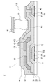
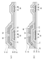
- Sectional drawing for demonstrating the transistor of an example of this invention, and the liquid crystal display device of an example of this invention (a)-(c): Sectional drawing for demonstrating the manufacturing process of the transistor of an example of this invention, and the liquid crystal display device of an example of this invention (1) (a)-(c): Sectional drawing for demonstrating the manufacturing process of the transistor of an example of this invention, and the liquid crystal display device of an example of this invention (2) (a), (b): Sectional drawing for demonstrating the manufacturing process of the transistor of an example of this invention, and the liquid crystal display device of an example of this invention (3) Sectional drawing (4) for demonstrating the manufacturing process of the transistor of an example of this invention, and the liquid crystal display device of an example of this invention
- Reference numeral 2 in FIG. 1 denotes a liquid crystal display device according to an embodiment of the present invention.
- a cross-sectional view of the transistor 11 of the first example of the present invention is shown together with a liquid crystal display portion 12. Yes.
- the transistor 11 will be described.
- an elongated gate electrode layer 32 is disposed on the surface of a glass substrate 31.
- a gate insulating film 33 is disposed at least in the width direction.
- a semiconductor layer 34 is disposed on the gate insulating film 33.
- the semiconductor layer 34 is located on both ends of the semiconductor layer 34 in the width direction of the gate electrode layer 32 and between the end of the gate electrode layer 32 and the gate insulating film 33.
- a source electrode layer 51 and a drain electrode layer 52 are formed at positions facing each other.
- a recess 55 is provided between the source electrode layer 51 and the drain electrode layer 52, and the source electrode layer 51 and the drain electrode layer 52 are separated by the recess 55 so that different voltages can be applied.
- a protective film 41 is formed on the source electrode layer 51, the drain electrode layer 52, and the recess 55 therebetween.
- a gate voltage is applied to the gate electrode layer 32 with a voltage applied between the source electrode layer 51 and the drain electrode layer 52, and the gate electrode layer 32 is interposed via the gate insulating film 33 in the semiconductor layer 34.
- a channel layer having a conductivity type opposite to the conductivity type of the semiconductor layer 34 (or a low resistance layer of the same conductivity type) is formed in a portion opposite to the semiconductor layer 34, a portion of the semiconductor layer 34 in contact with the source electrode layer 51 And a portion where the drain electrode layer 52 is in contact with each other by a channel layer (or a low resistance layer) with a low resistance.
- the source electrode layer 51 and the drain electrode layer 52 are electrically connected, and the transistor 11 becomes conductive. To do.
- the channel layer (or low resistance layer) disappears, and the source electrode layer 51 and the drain electrode layer 52 become high resistance and are electrically separated.
- a pixel electrode 82 is disposed on the liquid crystal display unit 12, and a liquid crystal 83 is disposed on the pixel electrode 82.
- An upper electrode 81 is positioned on the liquid crystal 83.
- the pixel electrode 82 is electrically connected to the source electrode layer 51 and the drain electrode layer 52, and voltage application to the pixel electrode 82 is started and ended when the transistor 11 is turned ON / OFF.
- the pixel electrode 82 is formed of a part of the transparent conductive layer 42 connected to the drain electrode layer 51.
- the transparent conductive layer 42 is made of ITO.
- a wiring layer 30 is disposed below the transparent conductive layer 42.
- the wiring layer 30 and the gate electrode layer 32 are composed of an adhesion film 37 made of Cu—Mg—Al, and a copper film mainly composed of copper formed on the adhesion film 37 (copper with a content exceeding 50 at%).
- the adhesion film 37 is in contact with the glass substrate 31, and the copper thin film 38 is not in contact with the glass substrate 31.
- a manufacturing process of the transistor 11 will be described.
- a glass substrate 31 as a film formation target is carried into a sputtering apparatus.
- a Cu—Mg—Al target and a pure copper target are provided in the sputtering apparatus, and the Cu—Mg—Al target is sputtered with a sputtering gas composed of a rare gas such as Ar gas, as shown in FIG.
- a sputtering gas composed of a rare gas such as Ar gas
- an adhesion film 37 is formed on the glass substrate 31, and then a pure copper target is sputtered by a sputtering gas composed of a rare gas, thereby forming a copper thin film 38 on the adhesion film 37.
- the adhesion film 37 and the copper thin film 38 oxygen gas is not introduced into the sputtering atmosphere, and copper oxide is not contained in the adhesion film 37 or the copper thin film 38, so that the low resistance adhesion film 37 and the copper thin film 38 are formed. It is formed. After forming the copper thin film 38, it may be annealed by heating to about 400 ° C. in a desired atmosphere.
- a patterned resist film 39 is disposed on the copper thin film 38, and an adhesion film 37 and a copper thin film 38 are etched in an etching solution capable of etching both pure copper and Cu—Mg—Al. 2 is immersed, and the copper thin film 38 exposed between the resist films 39 and the adhesion film 37 exposed after the etching of the copper thin film 38 are brought into contact with the same etching solution. As shown, the portion in contact with the etchant is removed by etching. Here, the copper thin film 38 and the adhesion film 37 are partially removed, and the gate electrode layer 32 and the wiring layer 30 are formed on the glass substrate 31 by the remaining portions.
- a gate insulating film 33 made of an insulating material such as SiO 2 or SiNx is formed on the surface of the glass substrate 31, the surface of the gate electrode layer 32, and the surface of the wiring layer 30.
- the gate insulating film 33 is patterned as necessary.
- a thin film made of a semiconductor material (for example, Si semiconductor or oxide semiconductor) is formed on the gate insulating film 33, patterned, and then patterned on the gate insulating film 33 as shown in FIG. 3B.
- a semiconductor layer 34 is formed.
- a metal thin film is formed on at least the surface of the semiconductor layer 34. The metal thin film is patterned to form a source electrode layer 51 and a drain electrode layer 52 as shown in FIG. Of the semiconductor layer 34, a portion that contacts the source electrode layer 51 is called a source region 71, and a portion that contacts the drain electrode layer 52 is called a drain region 72.
- the source electrode layer 51 and the drain electrode layer 52 are located on both ends of the semiconductor layer 34 in the width direction of the gate electrode layer 32 and are opposed to the end portion of the gate electrode layer 32 with the gate insulating film 33 interposed therebetween. Is arranged.
- a protective film 41 made of an insulating film such as SiNx or SiO 2 is formed.
- a connection hole 43 such as a via hole or a contact hole is formed in the protective film 41 or the gate insulating film 33, and the drain electrode layer 52, The surface of the copper thin film 38 included in the source electrode layer 51 or the wiring layer 30 is exposed, and in this state, a transparent conductive layer is formed and patterned.
- Reference numeral 42 in FIG. 5 indicates a patterned transparent conductive layer.
- the channel region 73 is a region of the semiconductor layer 34 between the source region 71 and the drain region 72, and the gate electrode layer 32 is at a position facing the channel region 73 with at least the gate insulating film 33 interposed therebetween.
- the transistor 11 is constituted in this way by the gate insulating film 33 and the gate / source / drain electrode layers 32, 51 and 52.
- the semiconductor layer 34 includes various semiconductors such as an oxide semiconductor such as InGaZnO, an amorphous semiconductor made of Si, a polycrystalline semiconductor, and a single crystal semiconductor.
- the laminated film of the adhesion film 37 and the copper thin film 38 was used for the wiring layer 30 and the gate electrode layer 32, when the source electrode layer and drain electrode layer of a MOS transistor are in contact with a glass substrate.
- the source electrode layer and the drain electrode layer can be constituted by a laminated film of the adhesion film 37 and the copper thin film 38.
- a target is prepared by containing Mg (magnesium) and Al (aluminum) in a desired ratio containing Cu (copper) as a main component, and sputtering the target, and Cu—Mg—Al having the same composition as the target on a glass substrate.
- a pure copper target was sputtered to form a pure copper thin film on the adhesion film, and a laminated film used as a gate electrode layer or a wiring layer was formed.
- the adhesion film was formed by changing the addition ratio of Mg and Al, and after forming a pure copper thin film, the adhesion between the electrode / wiring layer and the glass substrate was evaluated. The evaluation results are shown in Table 1 below. After the adhesion film and the pure copper thin film were formed, both the case where annealing was performed at 400 ° C. for 1 hour in a vacuum atmosphere and the case where it was not performed were measured.
- the numerical values in the columns of “Mg content” and “Al content” in Table 1 are obtained when the total number of Cu atoms, Mg atoms, and Al atoms in the target or adhesion film is 100 at%. , The Mg atom number ratio (Xat%) and the Al atom number ratio (Yat%) are shown, and “-” indicates a case where the content is zero.
- the column “Target availability” was classified as “ ⁇ ” when Cu, Mg, and Al materials could be formed on the target, and “ ⁇ ” when the target could not be formed.
- the evaluation in the “Adhesion” column is “ ⁇ ” when the adhesive tape is applied to the surface of the pure copper thin film, peeled off, and peeled off at the interface between the adhesive tape and the pure copper thin film. Or the separation at the interface between the electrode layer and the glass substrate was classified as “x”.
- the adhesion film 37 which is a thin film made of Cu—Mg—Al in each of the above embodiments of the present invention has a Mg content of 100 at% when the total number of Cu atoms, Mg atoms and Al atoms is 100 at%.
- the conductive thin film is desirably 0.5 at% or more and 5 at% or less and the Al content is 5 at% or more and 15 at% or less.
- the copper thin film 38 formed on the adhesion film 37 in contact with the adhesion film 37 is a low-resistance conductive material containing copper at a content exceeding 50 at% when the number of atoms of the copper thin film 38 is 100%. It is a thin film.
Landscapes
- Chemical & Material Sciences (AREA)
- Engineering & Computer Science (AREA)
- Materials Engineering (AREA)
- Mechanical Engineering (AREA)
- Metallurgy (AREA)
- Organic Chemistry (AREA)
- Thin Film Transistor (AREA)
- Electrodes Of Semiconductors (AREA)
- Internal Circuitry In Semiconductor Integrated Circuit Devices (AREA)
- Liquid Crystal (AREA)
Abstract
Description
アモルファスシリコンは低温で形成することができ、他の材料に悪影響を与えないが、移動度が低いという欠点があり、低温形成で高移動度の薄膜が大面積基板に形成できる酸化物半導体が注目されている。
そして近年では、高移動度の酸化物半導体に加え、半導体集積回路や、FPD中のトランジスタの電極層や配線層に低抵抗の銅薄膜を用い、大面積のFPDで輝度均一な表示を行うことも図られている。
特に、配線層やゲート電極層はガラス基板上に形成されるため、銅薄膜はガラスとの密着性が悪いことから、配線層やゲート電極層が剥離する虞がある。
この場合、銅薄膜とガラス基板の間に、銅配線のガラス基板に対する付着強度を増大させるTiN膜やW膜等の密着膜を設けることが行われているが、コストが高くなるという問題がある。
そのため、密着性を有し、且つ、銅薄膜と同じエッチング液によってエッチングできる密着膜が求められている。
本発明は、半導体層と、前記半導体層上に形成されたゲート絶縁膜と、前記ゲート絶縁膜を間にして前記半導体層と対向するゲート電極とを有し、前記半導体層には、前記ゲート電極と対向する部分にチャネル領域が設けられ、前記チャネル領域の両側にソース領域とドレイン領域とが設けられ、前記ソース領域と前記ドレイン領域には、ソース電極層とドレイン電極層がそれぞれ接触された半導体装置であって、前記ゲート電極層は、銅と、マグネシウムと、アルミニウムとを含有し、銅と、マグネシウムと、アルミニウムとの合計原子数を100at%としたとき、マグネシウムは0.5at%以上5at%以下、アルミニウムは5at%以上15at%以下の範囲にされた密着膜と、前記密着膜と接触して形成された銅薄膜とを有し、前記密着膜はガラス基板に接触された半導体装置である。
本発明の前記配線層と、前記ガラス基板とを有し、前記ガラス基板上には、画素電極と、前記画素電極上に位置する液晶と、前記液晶上に位置する上部電極とが配置され、前記画素電極は、前記配線層に電気的に接続された液晶表示装置である。
本発明の前記半導体装置と、前記ガラス基板とを有し、前記ガラス基板上には、画素電極と、前記画素電極上に位置する液晶と、前記液晶上に位置する上部電極とが配置され、前記画素電極は、前記ドレイン電極層又はソース電極層のいずれか一方に電気的に接続された液晶表示装置である。
密着膜とガラス基板との密着性は高いので、ガラス基板上に形成するゲート電極層や配線層が剥離することはない。
30……配線層
31……ガラス基板
32……ゲート電極層
33……ゲート絶縁膜
34……半導体層
37……密着膜
38……銅薄膜
43……接続孔
51……ソース電極層
52……ドレイン電極層
71……ソース領域
72……ドレイン領域
73……チャネル領域
81……上部電極
82……画素電極
83……液晶
このトランジスタ11を説明すると、該トランジスタ11は、ガラス基板31の表面に細長のゲート電極層32が配置されており、ゲート電極層32上には、少なくとも幅方向に亘ってゲート絶縁膜33が配置されている。
ゲート絶縁膜33上には、半導体層34が配置されており、半導体層34のうち、ゲート電極層32の幅方向両端上であって、ゲート電極層32の端部とゲート絶縁膜33を間に介して対向する位置に、ソース電極層51とドレイン電極層52とが形成されている。ソース電極層51とドレイン電極層52の間には凹部55が設けられ、この凹部55によってソース電極層51とドレイン電極層52とは分離されており、異なる電圧を印加できるように構成されいる。
ソース電極層51上と、ドレイン電極層52上と、その間の凹部55上には、保護膜41が形成されている。
ゲート電圧の印加を停止すると、チャネル層(又は低抵抗層)は消滅し、ソース電極層51とドレイン電極層52との間は高抵抗になり、電気的に分離される。
画素電極82はソース電極層51やドレイン電極層52と電気的に接続されており、トランジスタ11がON・OFFすることで、画素電極82への電圧印加の開始・終了が行われる。
ここでは画素電極82は、ドレイン電極層51に接続された透明導電層42の一部から成っている。透明導電層42はITOで構成されている。
この配線層30とゲート電極層32とは、Cu-Mg-Alから成る密着膜37と、密着膜37上に形成された銅を主成分とする銅膜(50at%を越える含有率で銅を含有する薄膜)とで構成されており、密着膜37はガラス基板31と接触しており、銅薄膜38はガラス基板31と接触しないようになっている。
このトランジスタ11は、先ず、成膜対象物のガラス基板31をスパッタリング装置内に搬入する。
スパッタリング装置内にはCu-Mg-Alターゲットと純銅ターゲットが設けられており、Arガス等の希ガスから成るスパッタリングガスでCu-Mg-Alターゲットをスパッタリングし、図2(a)に示すように、ガラス基板31上に密着膜37を形成し、次いで、希ガスから成るスパッタリングガスによって純銅ターゲットをスパッタリングして、密着膜37上に銅薄膜38を形成する。密着膜37と銅薄膜38を形成するときには、酸素ガスはスパッタリング雰囲気中に導入せず、密着膜37や銅薄膜38中に酸化銅を含有させないので、低抵抗の密着膜37と銅薄膜38が形成される。
銅薄膜38を形成した後、所望の雰囲気中で400℃程度に加熱してアニールしても良い。
パターニングしてゲート電極層32と配線層30を形成すると、ゲート電極層32と配線層30が位置する部分以外はガラス基板31の表面が露出しており、レジスト膜39を除去した後、図3(a)に示すように、ガラス基板31の表面、ゲート電極層32の表面、配線層30の表面に、SiO2、SiNx等の絶縁性材料から成るゲート絶縁膜33を形成する。このゲート絶縁膜33は、必要に応じてパターニングする。
次いで、少なくとも半導体層34の表面に金属薄膜が形成される。金属薄膜をパターニングして、図3(c)に示すように、ソース電極層51と、ドレイン電極層52とを形成する。半導体層34のうち、ソース電極層51と接触する部分がソース領域71と呼ばれ、ドレイン電極層52と接触する部分がドレイン領域72と呼ばれる。ソース電極層51とドレイン電極層52は、半導体層34のうち、ゲート電極層32の幅方向両端上であって、ゲート電極層32の端部とゲート絶縁膜33を間に介して対向する位置に配置されている。次いで、図4(a)に示すように、SiNxやSiO2等の絶縁膜から成る保護膜41を形成する。
そして、液晶83と上部電極81を後工程で配置して、図1に示す液晶表示装置2を得ると、トランジスタ11は動作可能な状態になる。
なお、半導体層34は、InGaZnO等の酸化物半導体や、Siから成るアモルファス半導体、多結晶半導体、単結晶半導体など、種々の半導体が含まれる。
また、上記実施例では、密着膜37と銅薄膜38の積層膜は、配線層30やゲート電極層32に用いたが、MOSトランジスタのソース電極層やドレイン電極層がガラス基板と接触する場合は、密着膜37と銅薄膜38の積層膜によってソース電極層やドレイン電極層を構成させることもできる。
密着膜は、MgとAlの添加割合を変えて形成し、次いで純銅薄膜を形成した後、電極・配線層とガラス基板との密着性を評価した。評価結果を下記表1に記載する。
密着膜と純銅薄膜とを形成した後、真空雰囲気中で400℃、1時間のアニールを行った場合と、行わなかった場合の両方を測定した。
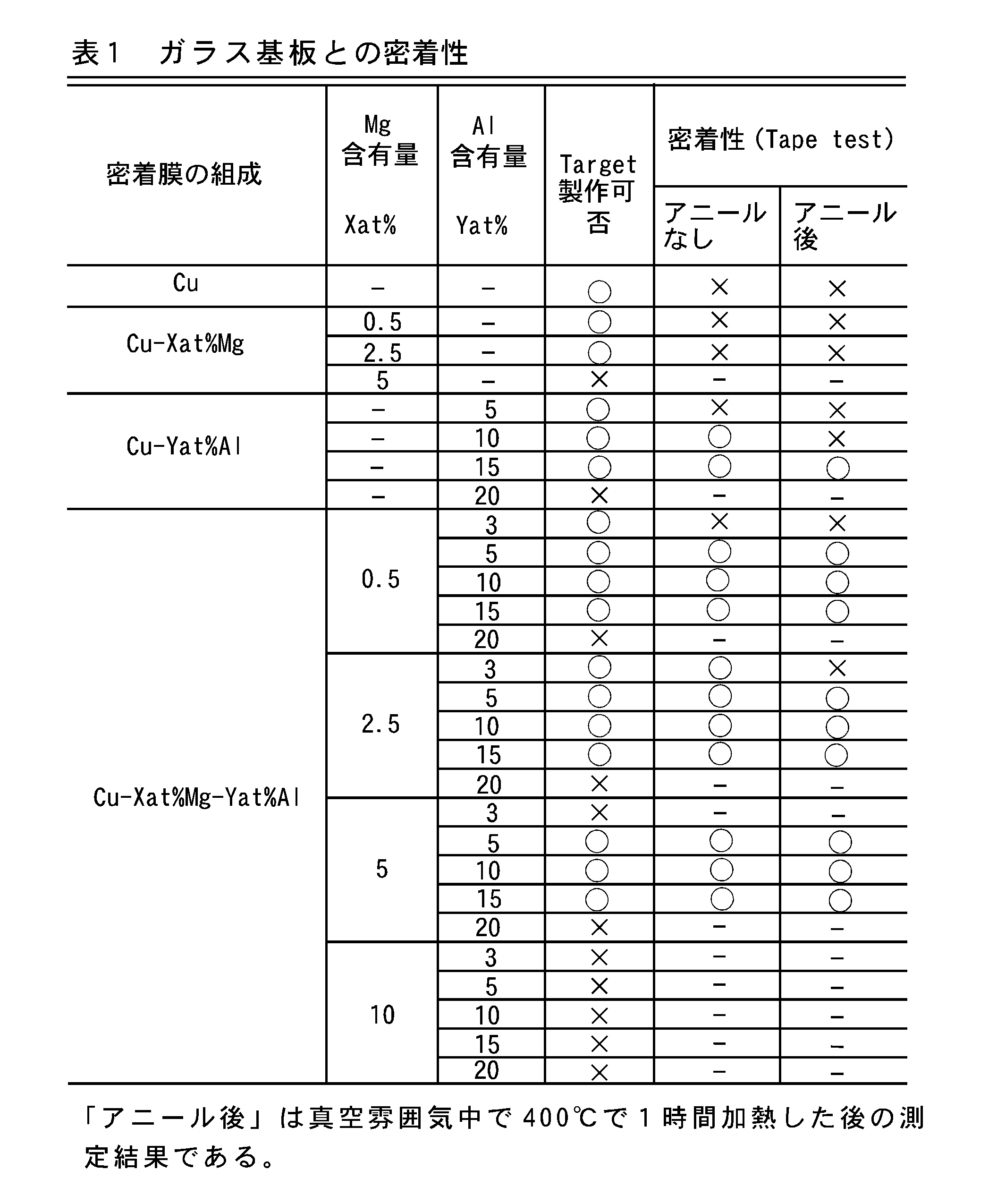
「Target作製可否」の欄は、Cu、Mg、Alの材料がターゲットに成形できた場合を“○”、ターゲットに成形できなかった場合を“×”に分類した。
密着膜37上に、密着膜37と接触して形成される銅薄膜38は、銅薄膜38の原子数を100%としたとき、50at%を越える含有率で銅を含有する低抵抗な導電性薄膜である。
Claims (4)
- ガラス基板と接触する配線層であって、
前記配線層は、
前記ガラス基板に接触する密着膜と、前記密着膜に接触する銅薄膜とから成り、
前記密着膜は、銅と、マグネシウムと、アルミニウムとを含有し、銅と、マグネシウムと、アルミニウムとの合計原子数を100at%としたとき、マグネシウムは0.5at%以上5at%以下、アルミニウムは5at%以上15at%以下の範囲にされた配線層。 - 半導体層と、
前記半導体層上に形成されたゲート絶縁膜と、
前記ゲート絶縁膜を間にして前記半導体層と対向するゲート電極とを有し、
前記半導体層には、前記ゲート電極と対向する部分にチャネル領域が設けられ、前記チャネル領域の両側にソース領域とドレイン領域とが設けられ、
前記ソース領域と前記ドレイン領域には、ソース電極層とドレイン電極層がそれぞれ接触された半導体装置であって、
前記ゲート電極層は、銅と、マグネシウムと、アルミニウムとを含有し、銅と、マグネシウムと、アルミニウムとの合計原子数を100at%としたとき、マグネシウムは0.5at%以上5at%以下、アルミニウムは5at%以上15at%以下の範囲にされた密着膜と、前記密着膜と接触して形成された銅薄膜とを有し、
前記密着膜はガラス基板に接触された半導体装置。 - 請求項1記載の配線層と、前記ガラス基板とを有し、前記ガラス基板上には、画素電極と、前記画素電極上に位置する液晶と、前記液晶上に位置する上部電極とが配置され、
前記画素電極は、前記配線層に電気的に接続された液晶表示装置。 - 請求項2記載の半導体装置と、前記ガラス基板とを有し、前記ガラス基板上には、画素電極と、前記画素電極上に位置する液晶と、前記液晶上に位置する上部電極とが配置され、
前記画素電極は、前記ドレイン電極層又はソース電極層のいずれか一方に電気的に接続された液晶表示装置。
Priority Applications (4)
| Application Number | Priority Date | Filing Date | Title |
|---|---|---|---|
| KR1020127002727A KR101175970B1 (ko) | 2009-08-28 | 2010-08-19 | 배선층, 반도체 장치, 액정 표시 장치 |
| JP2011528758A JP4970621B2 (ja) | 2009-08-28 | 2010-08-19 | 配線層、半導体装置、液晶表示装置 |
| CN201080039374.4A CN102484138B (zh) | 2009-08-28 | 2010-08-19 | 布线层、半导体装置、液晶显示装置 |
| US13/403,145 US8400594B2 (en) | 2009-08-28 | 2012-02-23 | Wiring layer, semiconductor device and liquid crystal display device |
Applications Claiming Priority (2)
| Application Number | Priority Date | Filing Date | Title |
|---|---|---|---|
| JP2009-198815 | 2009-08-28 | ||
| JP2009198815 | 2009-08-28 |
Related Child Applications (1)
| Application Number | Title | Priority Date | Filing Date |
|---|---|---|---|
| US13/403,145 Continuation US8400594B2 (en) | 2009-08-28 | 2012-02-23 | Wiring layer, semiconductor device and liquid crystal display device |
Publications (1)
| Publication Number | Publication Date |
|---|---|
| WO2011024704A1 true WO2011024704A1 (ja) | 2011-03-03 |
Family
ID=43627810
Family Applications (1)
| Application Number | Title | Priority Date | Filing Date |
|---|---|---|---|
| PCT/JP2010/063999 Ceased WO2011024704A1 (ja) | 2009-08-28 | 2010-08-19 | 配線層、半導体装置、液晶表示装置 |
Country Status (6)
| Country | Link |
|---|---|
| US (1) | US8400594B2 (ja) |
| JP (1) | JP4970621B2 (ja) |
| KR (1) | KR101175970B1 (ja) |
| CN (1) | CN102484138B (ja) |
| TW (1) | TWI379144B (ja) |
| WO (1) | WO2011024704A1 (ja) |
Cited By (4)
| Publication number | Priority date | Publication date | Assignee | Title |
|---|---|---|---|---|
| JP4913267B2 (ja) * | 2009-10-27 | 2012-04-11 | 株式会社アルバック | 配線層、半導体装置、半導体装置を有する液晶表示装置 |
| JP2015529012A (ja) * | 2012-07-20 | 2015-10-01 | 京東方科技集團股▲ふん▼有限公司 | アレイ基板の製造方法、アレイ基板及び表示装置 |
| JP2016219503A (ja) * | 2015-05-15 | 2016-12-22 | 株式会社アルバック | 半導体装置及びその製造方法、並びに実装デバイス |
| JP6768180B1 (ja) * | 2019-04-09 | 2020-10-14 | 株式会社アルバック | Cu合金ターゲット、配線膜、半導体装置、液晶表示装置 |
Families Citing this family (6)
| Publication number | Priority date | Publication date | Assignee | Title |
|---|---|---|---|---|
| KR102094841B1 (ko) | 2013-05-16 | 2020-03-31 | 삼성디스플레이 주식회사 | 표시 장치 및 이의 제조 방법 |
| KR20160148765A (ko) | 2015-06-16 | 2016-12-27 | 삼성디스플레이 주식회사 | 표시 장치 |
| WO2018189965A1 (ja) * | 2017-04-13 | 2018-10-18 | 株式会社アルバック | 液晶表示装置、有機el表示装置、半導体素子、配線膜、配線基板、ターゲット |
| WO2020183881A1 (ja) * | 2019-03-12 | 2020-09-17 | ソニーセミコンダクタソリューションズ株式会社 | 半導体装置 |
| CN110534530A (zh) * | 2019-08-15 | 2019-12-03 | 武汉华星光电半导体显示技术有限公司 | 显示面板及显示装置 |
| KR102989206B1 (ko) * | 2020-07-30 | 2026-07-09 | 삼성디스플레이 주식회사 | 디스플레이 장치 및 그 제조방법 |
Citations (4)
| Publication number | Priority date | Publication date | Assignee | Title |
|---|---|---|---|---|
| JPH1062799A (ja) * | 1996-08-21 | 1998-03-06 | Canon Inc | 配線基板、該配線基板の製造方法、該配線基板を備えた液晶素子及び該液晶素子の製造方法 |
| JPH1154458A (ja) * | 1997-05-08 | 1999-02-26 | Applied Materials Inc | メタライゼーション構造体 |
| WO2008081806A1 (ja) * | 2006-12-28 | 2008-07-10 | Ulvac, Inc. | 配線膜の形成方法、トランジスタ、及び電子装置 |
| JP2010053445A (ja) * | 2008-08-01 | 2010-03-11 | Mitsubishi Materials Corp | フラットパネルディスプレイ用配線膜形成用スパッタリングターゲット |
Family Cites Families (6)
| Publication number | Priority date | Publication date | Assignee | Title |
|---|---|---|---|---|
| US6037257A (en) | 1997-05-08 | 2000-03-14 | Applied Materials, Inc. | Sputter deposition and annealing of copper alloy metallization |
| KR100883769B1 (ko) * | 2002-11-08 | 2009-02-18 | 엘지디스플레이 주식회사 | 액정표시장치용 어레이기판 제조방법 |
| JP2008203808A (ja) | 2006-09-08 | 2008-09-04 | Mitsubishi Materials Corp | 熱欠陥発生がなくかつ密着性に優れたtftトランジスターを用いたフラットパネルディスプレイ用配線および電極並びにそれらを形成するためのスパッタリングターゲット |
| JP4496237B2 (ja) | 2007-05-14 | 2010-07-07 | 株式会社 日立ディスプレイズ | 液晶表示装置 |
| JP5234483B2 (ja) | 2007-06-12 | 2013-07-10 | 三菱マテリアル株式会社 | 密着性に優れた配線下地膜およびこの配線下地膜を形成するためのスパッタリングターゲット |
| KR101296654B1 (ko) * | 2007-12-26 | 2013-08-14 | 엘지디스플레이 주식회사 | 구리 배선, 이를 이용한 평판 표시 장치, 및 그 구리배선의 형성 방법 |
-
2010
- 2010-08-19 CN CN201080039374.4A patent/CN102484138B/zh active Active
- 2010-08-19 JP JP2011528758A patent/JP4970621B2/ja active Active
- 2010-08-19 WO PCT/JP2010/063999 patent/WO2011024704A1/ja not_active Ceased
- 2010-08-19 KR KR1020127002727A patent/KR101175970B1/ko active Active
- 2010-08-25 TW TW099128459A patent/TWI379144B/zh active
-
2012
- 2012-02-23 US US13/403,145 patent/US8400594B2/en active Active
Patent Citations (4)
| Publication number | Priority date | Publication date | Assignee | Title |
|---|---|---|---|---|
| JPH1062799A (ja) * | 1996-08-21 | 1998-03-06 | Canon Inc | 配線基板、該配線基板の製造方法、該配線基板を備えた液晶素子及び該液晶素子の製造方法 |
| JPH1154458A (ja) * | 1997-05-08 | 1999-02-26 | Applied Materials Inc | メタライゼーション構造体 |
| WO2008081806A1 (ja) * | 2006-12-28 | 2008-07-10 | Ulvac, Inc. | 配線膜の形成方法、トランジスタ、及び電子装置 |
| JP2010053445A (ja) * | 2008-08-01 | 2010-03-11 | Mitsubishi Materials Corp | フラットパネルディスプレイ用配線膜形成用スパッタリングターゲット |
Cited By (5)
| Publication number | Priority date | Publication date | Assignee | Title |
|---|---|---|---|---|
| JP4913267B2 (ja) * | 2009-10-27 | 2012-04-11 | 株式会社アルバック | 配線層、半導体装置、半導体装置を有する液晶表示装置 |
| JP2015529012A (ja) * | 2012-07-20 | 2015-10-01 | 京東方科技集團股▲ふん▼有限公司 | アレイ基板の製造方法、アレイ基板及び表示装置 |
| JP2016219503A (ja) * | 2015-05-15 | 2016-12-22 | 株式会社アルバック | 半導体装置及びその製造方法、並びに実装デバイス |
| JP6768180B1 (ja) * | 2019-04-09 | 2020-10-14 | 株式会社アルバック | Cu合金ターゲット、配線膜、半導体装置、液晶表示装置 |
| WO2020208904A1 (ja) * | 2019-04-09 | 2020-10-15 | 株式会社アルバック | Cu合金ターゲット、配線膜、半導体装置、液晶表示装置 |
Also Published As
| Publication number | Publication date |
|---|---|
| KR20120062692A (ko) | 2012-06-14 |
| JP4970621B2 (ja) | 2012-07-11 |
| CN102484138A (zh) | 2012-05-30 |
| US20120194757A1 (en) | 2012-08-02 |
| TW201202817A (en) | 2012-01-16 |
| JPWO2011024704A1 (ja) | 2013-01-31 |
| CN102484138B (zh) | 2014-03-12 |
| TWI379144B (en) | 2012-12-11 |
| KR101175970B1 (ko) | 2012-08-22 |
| US8400594B2 (en) | 2013-03-19 |
Similar Documents
| Publication | Publication Date | Title |
|---|---|---|
| JP4970621B2 (ja) | 配線層、半導体装置、液晶表示装置 | |
| JP4970622B2 (ja) | 半導体装置、半導体装置を有する液晶表示装置、半導体装置の製造方法 | |
| JP5579848B2 (ja) | 半導体装置、半導体装置を有する液晶表示装置、半導体装置の製造方法 | |
| CN101529566B (zh) | 布线膜的形成方法、晶体管及电子装置 | |
| JP4913267B2 (ja) | 配線層、半導体装置、半導体装置を有する液晶表示装置 | |
| JP6768180B1 (ja) | Cu合金ターゲット、配線膜、半導体装置、液晶表示装置 | |
| JP2020012190A (ja) | 密着膜用ターゲット、配線層、半導体装置、液晶表示装置 | |
| JP2011091365A (ja) | 配線構造およびその製造方法、並びに配線構造を備えた表示装置 | |
| JPWO2020213232A1 (ja) | Cu合金ターゲット |
Legal Events
| Date | Code | Title | Description |
|---|---|---|---|
| WWE | Wipo information: entry into national phase |
Ref document number: 201080039374.4 Country of ref document: CN |
|
| 121 | Ep: the epo has been informed by wipo that ep was designated in this application |
Ref document number: 10811754 Country of ref document: EP Kind code of ref document: A1 |
|
| WWE | Wipo information: entry into national phase |
Ref document number: 2011528758 Country of ref document: JP |
|
| ENP | Entry into the national phase |
Ref document number: 20127002727 Country of ref document: KR Kind code of ref document: A |
|
| NENP | Non-entry into the national phase |
Ref country code: DE |
|
| 122 | Ep: pct application non-entry in european phase |
Ref document number: 10811754 Country of ref document: EP Kind code of ref document: A1 |