WO2011007832A1 - 成膜装置 - Google Patents
成膜装置 Download PDFInfo
- Publication number
- WO2011007832A1 WO2011007832A1 PCT/JP2010/061980 JP2010061980W WO2011007832A1 WO 2011007832 A1 WO2011007832 A1 WO 2011007832A1 JP 2010061980 W JP2010061980 W JP 2010061980W WO 2011007832 A1 WO2011007832 A1 WO 2011007832A1
- Authority
- WO
- WIPO (PCT)
- Prior art keywords
- target
- film
- processed
- forming apparatus
- substrate
- Prior art date
- Legal status (The legal status is an assumption and is not a legal conclusion. Google has not performed a legal analysis and makes no representation as to the accuracy of the status listed.)
- Ceased
Links
Images



Classifications
-
- C—CHEMISTRY; METALLURGY
- C23—COATING METALLIC MATERIAL; COATING MATERIAL WITH METALLIC MATERIAL; CHEMICAL SURFACE TREATMENT; DIFFUSION TREATMENT OF METALLIC MATERIAL; COATING BY VACUUM EVAPORATION, BY SPUTTERING, BY ION IMPLANTATION OR BY CHEMICAL VAPOUR DEPOSITION, IN GENERAL; INHIBITING CORROSION OF METALLIC MATERIAL OR INCRUSTATION IN GENERAL
- C23C—COATING METALLIC MATERIAL; COATING MATERIAL WITH METALLIC MATERIAL; SURFACE TREATMENT OF METALLIC MATERIAL BY DIFFUSION INTO THE SURFACE, BY CHEMICAL CONVERSION OR SUBSTITUTION; COATING BY VACUUM EVAPORATION, BY SPUTTERING, BY ION IMPLANTATION OR BY CHEMICAL VAPOUR DEPOSITION, IN GENERAL
- C23C14/00—Coating by vacuum evaporation, by sputtering or by ion implantation of the coating forming material
- C23C14/22—Coating by vacuum evaporation, by sputtering or by ion implantation of the coating forming material characterised by the process of coating
- C23C14/34—Sputtering
- C23C14/35—Sputtering by application of a magnetic field, e.g. magnetron sputtering
-
- H—ELECTRICITY
- H10—SEMICONDUCTOR DEVICES; ELECTRIC SOLID-STATE DEVICES NOT OTHERWISE PROVIDED FOR
- H10P—GENERIC PROCESSES OR APPARATUS FOR THE MANUFACTURE OR TREATMENT OF DEVICES COVERED BY CLASS H10
- H10P14/00—Formation of materials, e.g. in the shape of layers or pillars
- H10P14/40—Formation of materials, e.g. in the shape of layers or pillars of conductive or resistive materials
- H10P14/42—Formation of materials, e.g. in the shape of layers or pillars of conductive or resistive materials using a gas or vapour
-
- C—CHEMISTRY; METALLURGY
- C23—COATING METALLIC MATERIAL; COATING MATERIAL WITH METALLIC MATERIAL; CHEMICAL SURFACE TREATMENT; DIFFUSION TREATMENT OF METALLIC MATERIAL; COATING BY VACUUM EVAPORATION, BY SPUTTERING, BY ION IMPLANTATION OR BY CHEMICAL VAPOUR DEPOSITION, IN GENERAL; INHIBITING CORROSION OF METALLIC MATERIAL OR INCRUSTATION IN GENERAL
- C23C—COATING METALLIC MATERIAL; COATING MATERIAL WITH METALLIC MATERIAL; SURFACE TREATMENT OF METALLIC MATERIAL BY DIFFUSION INTO THE SURFACE, BY CHEMICAL CONVERSION OR SUBSTITUTION; COATING BY VACUUM EVAPORATION, BY SPUTTERING, BY ION IMPLANTATION OR BY CHEMICAL VAPOUR DEPOSITION, IN GENERAL
- C23C14/00—Coating by vacuum evaporation, by sputtering or by ion implantation of the coating forming material
- C23C14/22—Coating by vacuum evaporation, by sputtering or by ion implantation of the coating forming material characterised by the process of coating
- C23C14/34—Sputtering
-
- H—ELECTRICITY
- H01—ELECTRIC ELEMENTS
- H01J—ELECTRIC DISCHARGE TUBES OR DISCHARGE LAMPS
- H01J37/00—Discharge tubes with provision for introducing objects or material to be exposed to the discharge, e.g. for the purpose of examination or processing thereof
- H01J37/32—Gas-filled discharge tubes
- H01J37/34—Gas-filled discharge tubes operating with cathodic sputtering
- H01J37/3402—Gas-filled discharge tubes operating with cathodic sputtering using supplementary magnetic fields
- H01J37/3405—Magnetron sputtering
- H01J37/3408—Planar magnetron sputtering
-
- H—ELECTRICITY
- H01—ELECTRIC ELEMENTS
- H01J—ELECTRIC DISCHARGE TUBES OR DISCHARGE LAMPS
- H01J37/00—Discharge tubes with provision for introducing objects or material to be exposed to the discharge, e.g. for the purpose of examination or processing thereof
- H01J37/32—Gas-filled discharge tubes
- H01J37/34—Gas-filled discharge tubes operating with cathodic sputtering
- H01J37/3411—Constructional aspects of the reactor
- H01J37/3447—Collimators, shutters, apertures
-
- H—ELECTRICITY
- H10—SEMICONDUCTOR DEVICES; ELECTRIC SOLID-STATE DEVICES NOT OTHERWISE PROVIDED FOR
- H10P—GENERIC PROCESSES OR APPARATUS FOR THE MANUFACTURE OR TREATMENT OF DEVICES COVERED BY CLASS H10
- H10P14/00—Formation of materials, e.g. in the shape of layers or pillars
- H10P14/40—Formation of materials, e.g. in the shape of layers or pillars of conductive or resistive materials
- H10P14/42—Formation of materials, e.g. in the shape of layers or pillars of conductive or resistive materials using a gas or vapour
- H10P14/44—Physical vapour deposition [PVD]
Definitions
- the present invention relates to a film forming apparatus for forming a film on the surface of an object to be processed, and more particularly to a film forming apparatus using a sputtering method which is a kind of thin film forming method.
- a film forming apparatus using a sputtering method (hereinafter referred to as a “sputtering apparatus”) is used in a film forming process in manufacturing a semiconductor device.
- a sputtering apparatus with the recent miniaturization of the wiring pattern, over the entire surface of the substrate to be processed, high aspect ratio fine holes and trenches with a depth to width ratio of more than 3 can be used. Therefore, it is strongly required to form a film with good coverage, that is, to improve the coverage.
- a negative voltage is applied to a target arranged in a vacuum chamber into which argon gas has been introduced (hereinafter referred to as ignition) as a first step for causing sputtered particles to jump out of the target.
- sputtering gas for example, argon gas
- sputtered particles are ejected from the target surface by the collision.
- Cu atoms jump out as sputtered particles from a target formed of a wiring thin film material such as Cu, and adhere to the substrate to form a thin film.
- the substrate to be deposited is disposed in the vacuum chamber so as to face the target at a predetermined interval.
- a magnetic field is formed on the target surface by a magnetic field generating means (for example, a permanent magnet) provided on the back surface of the target. Then, by applying a negative voltage to the target, sputtering gas ions collide with the target surface, and target material atoms and secondary electrons are knocked out. By circulating these secondary electrons in the magnetic field formed on the target surface, the frequency of ionization collision between the sputtering gas (inert gas such as argon gas) and the secondary electrons is increased, the plasma density is increased, and the thin film Formation is possible (for example, refer patent document 1).
- a magnetic field generating means for example, a permanent magnet
- the applicant has a great influence on the occurrence of aggregation of the fine hole and trench side walls immediately after applying a negative potential to the target and when the plasma is not stable. I found out what it was doing.
- the cause of this aggregation is thought to be the initial film quality formed by the sputtered particles before the plasma is stabilized.
- a defect in the film quality at the initial stage affected the film formation after the plasma was stabilized, resulting in a film quality defect.
- the film thickness to be formed was relatively large, the amount of film formed at the time of ignition was relatively small, which was not a problem.
- the film thickness formed at the time of ignition cannot be ignored with respect to the required film thickness.
- the present invention can form a film with good coverage on each fine hole and trench having a high aspect ratio formed on a substrate without being affected by sputtered particles deposited at the time of ignition. It is an object of the present invention to provide a possible film forming apparatus.
- a film forming apparatus is a film forming apparatus that forms a film on a surface of an object to be processed using a sputtering method, and the object to be processed and the film disposed so as to face each other.
- a chamber for storing a target as a base material; an exhaust means for depressurizing the inside of the chamber; a magnetic field generating means for generating a magnetic field in front of the sputtering surface of the target; and a DC power source for applying a negative DC voltage to the target
- Gas introduction means for introducing a sputtering gas into the chamber; means for preventing the sputter particles from entering the object to be processed until the plasma generated between the target and the object to be processed becomes stable. And comprising;
- the means may be a shutter disposed between the object to be processed and the target.
- the means may be a transport device that moves the object to be processed in the horizontal direction below the target.
- the means may be a grid electrode capable of forming an electric field between the object to be processed and the target.
- the means may be a magnetic field generating means for forming a magnetic field between the target object and the target so as to deviate the trajectory of the sputtered particles from the target object.
- the apparatus in a film forming apparatus that forms a coating film on a surface of an object to be processed using a sputtering method, includes a means for preventing incidence of sputtered particles on the object to be processed until the plasma becomes stable. Accordingly, it is possible to form a film with good coverage on each fine hole and trench having a high aspect ratio formed on the substrate without being affected by the sputtered particles formed at the time of ignition. In the case where a shutter disposed between the object to be processed and the target is employed as the above means, since the shutter blocks the sputtered particles, the film can be formed without being affected by the sputtered particles at the time of ignition.
- the film forming apparatus 1 is of a DC magnetron sputtering method and includes a vacuum chamber 2 capable of forming a vacuum atmosphere.
- a cathode unit C is attached to the ceiling of the vacuum chamber 2.
- the ceiling side of the vacuum chamber 2 is referred to as “upper” and the bottom side thereof is referred to as “lower”.
- the cathode unit C includes a target 3, and the target 3 is attached to a holder 5. Further, the cathode unit C includes magnetic field generating means 4 that generates a tunnel-like magnetic field in front of the sputtering surface (lower surface) 3 a of the target 3.
- the target 3 is made of a material appropriately selected according to the composition of the thin film to be formed on the substrate W (object to be processed), for example, Cu, Ti, Al, or Ta.
- the target 3 is produced in a predetermined shape (for example, a circular shape in plan view) by a known method so that the area of the sputtering surface 3a is larger than the surface area of the substrate W in accordance with the shape of the substrate W to be processed.
- the target 3 is electrically connected to a DC power source (sputtering power source) 9 having a known structure so that a predetermined negative potential is applied.
- the magnetic field generating means 4 is disposed on the surface (upper surface) opposite to the sputtering surface 3 a of the target 3.
- the magnetic field generating means 4 includes a yoke 4a disposed in parallel with the target 3 and magnets 4b and 4c disposed on the lower surface of the yoke 4a so that the polarities on the target 3 side are different from each other.
- the shape and number of the magnets 4b and 4c are appropriately selected according to the magnetic field to be formed in front of the target 3 from the viewpoint of stability of discharge and improvement in use efficiency of the target.
- a flaky or rod-shaped magnet may be used, or these may be used in appropriate combination.
- the magnetic field generating means 4 may be configured to reciprocate or rotate on the back side of the target 3.
- a stage 10 is disposed at the bottom of the vacuum chamber 2 so as to face the target 3 so that the substrate W can be positioned and held.
- a gas pipe 11 for introducing a sputtering gas such as argon gas is connected to the side wall of the vacuum chamber 2, and the other end communicates with a gas source via a mass flow controller (not shown).
- the vacuum chamber 2 is connected to an exhaust pipe 12a communicating with a vacuum exhaust means 12 (exhaust means) such as a turbo molecular pump or a rotary pump.
- a rotary shaft 20 is inserted in an airtight manner in the bottom wall of the vacuum chamber 2, and a shutter 21 is attached to the tip portion thereof.
- the rotating shaft 20 can be rotated by power such as a motor (not shown).
- the shutter 21 is disposed between the substrate W and the shield 22. By rotating the rotating shaft 20, the substrate W can be completely covered with the shutter 21 when viewed from the target 3 side, and the substrate W can be completely exposed when viewed from the target 3 side.
- the evacuation unit 12 is operated to evacuate the vacuum chamber 2 to a predetermined degree of vacuum (for example, a pressure of 10 ⁇ 5 Pa level). Then, after the pressure in the vacuum chamber 2 reaches a predetermined value, the substrate W is set on the stage 10 and the shutter 21 is disposed above the substrate W. While introducing argon gas (sputtering gas) or the like into the vacuum chamber 2 at a predetermined flow rate, a predetermined negative potential is applied (powered on) to the target 3 from the DC power source 9 to form a plasma atmosphere in the vacuum chamber 2. To do.
- argon gas sputtering gas
- a predetermined negative potential is applied (powered on) to the target 3 from the DC power source 9 to form a plasma atmosphere in the vacuum chamber 2.
- Argon ions in the plasma collide with the sputter surface 3a and the sputter surface 3a is sputtered, and sputter atoms and sputter ions (sputter particles) are scattered from the sputter surface 3a toward the substrate W.
- the shutter 21 is disposed immediately above the substrate W, the sputtered particles only adhere to the shutter 21 and do not reach the substrate W.
- the rotating shaft 20 is rotated to move the shutter 21 from directly above the substrate W, so that the substrate W is exposed to the target 3. As a result, the sputtered particles reach the substrate W, and film formation is started.
- the shutter 21 by blocking the sputtered particles in the initial stage of sputtering by the shutter 21, the sputtered particles when the plasma is unstable do not reach the substrate W. For this reason, it becomes possible to form a film with good coverage on each fine hole and trench having a high aspect ratio formed on the substrate.
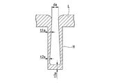
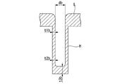
- FIG. 8A and 8B are schematic cross-sectional views of the formed high aspect ratio fine holes.
- H is a fine hole with a high aspect ratio
- L is a thin film formed.
- the substrate W to be formed can be obtained by forming a silicon oxide film (insulating film) I on the surface of the Si wafer and then patterning fine holes H having a high aspect ratio in the silicon oxide film.
- FIG. 8A is a schematic cross-sectional view of the fine hole H when the film formation at the time of ignition is not blocked
- FIG. 8B is a schematic cross-sectional view of the fine hole H when the film formation at the time of ignition is cut off.
- FIG. 8A is a schematic cross-sectional view of the fine hole H when the film formation at the time of ignition is not blocked
- FIG. 8B is a schematic cross-sectional view of the fine hole H when the film formation at the time of ignition is cut off.
- FIG. 8A it can be seen that the upper film thickness t1a and the lower film thickness t2a of the fine hole H are not uniform.
- FIG. 8B it can be seen that the film thickness t1b at the upper part and the film thickness t2b at the lower part of the fine hole H are substantially uniform by blocking the film formation at the time of ignition. Further, comparing the opening diameter da of FIG. 8A and the opening diameter db of FIG. 8B, it can be seen that a larger diameter db is secured in FIG. 8B. Further, when the film thickness t3a at the bottom of the fine hole H in FIG. 8A is compared with the film thickness t3b in FIG. 8B, it can be seen that a sufficient film thickness t3b is ensured in FIG. . Furthermore, it can be seen that the unevenness (morphology) of the film attached to the side wall is improved in FIG. 8B compared to FIG. 8A.
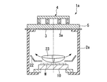
- FIG. 1A is schematic views of the film forming apparatus 1a including the split shutter 23.
- the film forming apparatus 1 a includes a split shutter 23 having a circular shape in plan view that can be split into two at the center between the target 3 and the substrate W.
- the division shutter 23 Before the division, the division shutter 23 has a sufficient size to block the sputtered particles popping out from the target 3 with respect to the substrate W as shown in FIG. 2A.
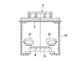
- the divided shutter 23 is configured to be swingable so as to draw an arc after the division.
- the divided shutter 23 can be opened and closed so that the substrate W is exposed to the target 3 after the ignition. .
- the film forming apparatus 1a of the present embodiment covers each fine hole and trench having a high aspect ratio formed on the substrate W without being affected by the sputtered particles formed at the time of ignition. It is possible to perform film formation with good properties.
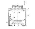
- FIG. 1B are schematic views of the film forming apparatus 1b including the movable shutter 24.
- FIG. The film forming apparatus 1b is characterized in that a movable shutter 24 is movably installed between the target 3 and the substrate W.
- the movable shutter 24 has a rectangular plate shape in plan view, and one side of the movable shutter 24 is connected to the movable shaft 25 via a hinge part 26.
- the movable shaft 25 is hermetically inserted through the bottom wall of the chamber 2 and is configured to be movable up and down by power means (not shown).
- FIG. 3A is a view when the movable shaft 25 is positioned at the lowermost part.
- the movable shutter 24 is guided directly above the substrate W by a guide (not shown) so that the substrate W is not exposed to the target.
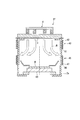
- FIG. 3B is a view when the movable shaft 25 is positioned at the uppermost part, and the movable shutter 24 rotates around the hinge portion 26 along the side wall of the chamber 2a. As a result, the substrate W is exposed to the target 3 and the sputtered particles reach the substrate W.
- FIG. 4A and 4B are schematic views of a film forming apparatus 1c having a movable stage 10a.
- the movable stage 10a is disposed at the bottom of the vacuum chamber 2b, and can position and hold the substrate W as in the first embodiment.
- the movable stage 10a is movable in the horizontal direction by power means (not shown).
- 4A the movable stage 10a is placed at a position where the substrate W is not exposed to the target 3 and at a position where the substrate W is exposed to the target 3 as shown in FIG. 4B. Can be moved.
- the substrate W is set on the movable stage 10a. At this time, the substrate W is placed at a position where it is not exposed to the target 3. Then, a predetermined negative potential is applied (powered on) to the target 3 from the DC power source to form a plasma atmosphere in the vacuum chamber 2.
- Argon ions in the plasma collide with the sputter surface 3a and the sputter surface 3a is sputtered, and sputter atoms and sputter ions (sputter particles) are scattered from the sputter surface 3a toward the substrate W.
- the substrate W is disposed at a position where it is not exposed to the target 3, the sputtered particles do not reach the substrate W.
- the movable stage 10a is moved.
- the substrate W held on the movable stage 10a moves to the center of the vacuum chamber 2b in plan view, the substrate W is exposed to the target 3.
- the sputtered particles reach the substrate W, and film formation is started.
- the substrate W by arranging the substrate W at a position where it is not exposed to the target 3 in the initial stage of sputtering, the sputtered particles when the plasma is unstable do not reach the substrate W. For this reason, it becomes possible to form a film with good coverage on each fine hole and trench having a high aspect ratio formed on the substrate W.
- FIG. 5 is a schematic view of a film forming apparatus 1d provided with a continuous stage 10b.
- the continuous stage 10b has a configuration in which a plurality of stages are connected, and is arranged at the bottom of the vacuum chamber 2c.
- the continuous stage 10b can freely move in the vacuum chamber 2c like a belt conveyor.
- a substrate W is placed on each stage constituting the continuous stage 10b. However, the dummy substrate Wd is placed on the top stage.
- the substrate W is set on each stage of the continuous stage 10b.
- a dummy substrate Wd is placed on the first stage.
- a predetermined negative potential is applied (powered on) to the target 3 from a DC power source to form a plasma atmosphere in the vacuum chamber 2.
- Argon ions in the plasma collide with the sputter surface 3a and the sputter surface 3a is sputtered, and sputter atoms and sputter ions (sputter particles) are scattered from the sputter surface 3a toward the substrate W.
- sputtered particles are deposited on the dummy substrate Wd to form a film.
- the continuous stage 10b is moved to deposit the sputtered particles from the stable plasma on the substrate W to form a film.
- the continuous stage 10b moves.
- FIGS. 6A and 6B are schematic views of a film forming apparatus 1e provided with a mesh electrode 30.
- the film forming apparatus 1e includes a mesh electrode 30 between the target 3 and the substrate W, and the mesh electrode 30 is fixed in the vacuum chamber 2a by an appropriate method.
- FIG. 6B shows a plan view of the mesh electrode 30.
- the mesh electrode 30 is composed of a frame body 31 and a conducting wire 32 that are circular in plan view, and the conducting wires 32 are fixed in a lattice shape within the frame body 31. It is preferable that the conducting wire 32 used is as thin as possible so as not to inhibit the passage of sputtered particles.
- the mesh electrode 30 is connected to a power source (not shown), and an electromagnetic field can be formed by applying a voltage from the power source.
- the film forming apparatus 1e configured as described above can block sputtered particles and charged particles during film formation at the time of ignition by forming an electromagnetic field around the mesh electrode 30 by the mesh electrode 30 at the time of ignition. Further, since the mesh electrode 30 used in the film forming apparatus 1e does not need to use a specially-shaped vacuum chamber, it can be easily introduced into an existing film forming apparatus.
- FIG. 7 is a schematic diagram of a film forming apparatus 1 f including the first coil 40 and the second coil 45.
- the magnetic lines of force M are shown using arrows in FIG. 7 for convenience of explanation, but do not limit the direction of the magnetic field.
- the direction may be N ⁇ S or may be S ⁇ N.
- the film forming apparatus 1f is provided with a first coil 40 and a second coil 45 around the vacuum chamber 2a.
- the first coil 40 and the second coil 45 have ring-shaped coil supports 41 and 46 provided on the outer wall of the vacuum chamber 2 with predetermined intervals in the vertical direction, respectively.
- conductive wires 42 and 47 are wound around a vertical axis connecting the center of the target 3 and the substrate W, respectively.
- Each of the coils 40 and 45 includes a power supply device (not shown) that can energize the coils 40 and 45.
- the number of coils, the diameter and the number of turns of the conducting wire 15 are, for example, the size of the target 3, the distance between the target 3 and the substrate W, the rated current value of the power supply device, and the strength of the magnetic field to be generated (Gauss). It is set appropriately according to
- the power supply device has a known structure including a control circuit (not shown) that can arbitrarily change the current value and the current direction in the first coil 40 and the second coil 45.
- a negative current value is applied to the first coil 40 so that a downward vertical magnetic field is generated.
- a positive current value was applied to the second coil 45 so as to generate an upward vertical magnetic field.
- the film forming apparatus 1 f during ignition, a negative current is applied to the first coil 40 and a positive current is applied to the second coil 45, so that the trajectory of the sputtered particles is formed between the substrate W and the target 3.
- a negative current is applied to the first coil 40
- a positive current is applied to the second coil 45, so that the trajectory of the sputtered particles is formed between the substrate W and the target 3.
- the coils 40 and 45 used in the film forming apparatus 1f of the present embodiment do not require a specially-shaped vacuum chamber, and therefore can be easily introduced into an existing film forming apparatus.
Landscapes
- Chemical & Material Sciences (AREA)
- Engineering & Computer Science (AREA)
- Physics & Mathematics (AREA)
- Plasma & Fusion (AREA)
- Analytical Chemistry (AREA)
- Chemical Kinetics & Catalysis (AREA)
- Materials Engineering (AREA)
- Mechanical Engineering (AREA)
- Metallurgy (AREA)
- Organic Chemistry (AREA)
- Physical Vapour Deposition (AREA)
- Electrodes Of Semiconductors (AREA)
Abstract
Description
本願は、2009年7月17日に、日本に出願された特願2009-169335号に基づき優先権を主張し、その内容をここに援用する。
配線パターンが微細化する以前は、成膜する膜厚が比較的厚かったため、イグニッション時に成膜される成膜量は相対的に小さく、問題とはならなかった。しかし、近年、配線パターンが微細化したことによって、要求される膜厚に対して、着火時(イグニッション時)に形成される膜厚が無視できなくなってきた。
あるいは、前記手段が、前記被処理体を前記ターゲット下方において水平方向に移動させる輸送装置であってもよい。
また、前記手段が、前記被処理体と前記ターゲットとの間に電場を形成することが可能な格子状の電極であってもよい。
また、前記手段が、前記被処理体と前記ターゲットとの間に前記スパッタ粒子の軌道を前記被処理体から逸らせるような磁場を形成する、磁場発生手段であってもよい。
上記手段に被処理体とターゲットとの間に配置されたシャッタを採用した場合には、シャッタがスパッタ粒子を遮断するため、イグニッション時のスパッタ粒子の影響を受けずに成膜することができる。
以下、図面を参照して本発明の第1の実施形態に係る成膜装置について説明する。図1に示すように、成膜装置1は、DCマグネトロンスパッタリング方式のものであり、真空雰囲気の形成が可能な真空チャンバ2を備える。真空チャンバ2の天井部にはカソードユニットCが取り付けられている。なお、以下においては、真空チャンバ2の天井部側を「上」とし、その底部側を「下」として説明する。
シャッタ21は、基板Wとシールド22との間に配置されている。回転軸20を回転させることにより、ターゲット3側から見て、基板Wをシャッタ21により完全に覆うことができ、ターゲット3側から見て、基板Wを完全に露出させることもできる。
まず、真空排気手段12を作動させて真空チャンバ2内を所定の真空度(例えば、10-5Pa台の圧力)まで真空引きする。そして、真空チャンバ2内の圧力が所定値に達した後、ステージ10に基板Wをセットし、シャッタ21を基板Wの上方に配置する。真空チャンバ2内にアルゴンガスなど(スパッタガス)を所定の流量で導入しつつ、DC電源9よりターゲット3に所定の負の電位を印加(電力投入)して真空チャンバ2内にプラズマ雰囲気を形成する。この場合、磁場発生手段4からの磁場で、スパッタ面3a前方で電離した電子及びスパッタリングによって生じた二次電子が捕捉され、スパッタ面3a前方におけるプラズマが高密度となる。
スパッタリング初期段階が終了しプラズマが安定した段階で、回転軸20を回転させることによって、シャッタ21が基板Wの直上から移動し、基板Wがターゲット3に対して露出される。これにより、スパッタ粒子は基板Wまで到達し、成膜が開始される。
特に、Cuターゲットの場合には、自己保持放電が可能である。このためスパッタガス導入による着火後、スパッタガス導入をやめて、プラズマが安定に維持されるまで待ち、その後シャッタ21を開放し、基板Wに成膜を開始することも可能である。
図8Aは、イグニッション時の成膜を遮断しなかった場合の微細ホールHの模式断面図であり、図8Bは、イグニッション時の成膜を遮断した場合の微細ホールHの模式断面図である。
図8Aでは、微細ホールHの上部の膜厚t1aと下部の膜厚t2aとが不均一であることがわかる。一方、図8Bでは、イグニッション時の成膜を遮断したことによって、微細ホールHの上部の膜厚t1bと下部の膜厚t2bとが略均一であることがわかる。
また、図8Aの開口部径daと図8Bの開口部径dbとを比較すると、図8Bにおいてより大きな径dbが確保されることがわかる。さらに、図8Aの微細ホールH底部の膜厚t3aと、図8Bの膜厚t3bとを比較すると、図8Bにおいて十分な膜厚t3bが確保されており、ボトムカバレッジが改善されていることがわかる。
さらに、側壁に付着した膜の凹凸(モホロジー)が、図8Aに比べて図8Bでは改善されることがわかる。
分割シャッタを使用する、本発明の第2の実施形態について説明する。本実施形態においても、第1の実施形態と同様にイグニッション時のスパッタ粒子を遮断するためのシャッタが用いられている。本実施形態は、シャッタ機構に関し第1の実施形態のシャッタ21の代わりに分割シャッタ23が用いられていることを除き、第1の実施形態と同様の構成を有している。図2A及び図2Bは、分割シャッタ23を備えた、成膜装置1aの概略図である。
成膜装置1aはターゲット3と基板Wとの間に、中央部において2つに分割可能な平面視円形の分割シャッタ23を備えている。分割シャッタ23は、分割前においては、図2Aに示すように、基板Wに対して、ターゲット3から飛び出してくるスパッタ粒子を遮断するのに十分な大きさを有している。
分割シャッタ23は、分割後は弧を描くように揺動可能に構成されており、図2Bに示すように、イグニッション後に、ターゲット3に対して基板Wを露出するように、開閉が可能である。
このような構成によって、本実施形態の成膜装置1aは、イグニッション時に成膜されるスパッタ粒子の影響を受けずに、基板Wに形成された高アスペクト比の各微細ホール及びトレンチに対し、被覆性の良い成膜を行うことが可能である。
可動シャッタを使用する、本発明の第3の実施形態について説明する。本実施形態においても、第1の実施形態と同様にイグニッション時のスパッタ粒子を遮断するためのシャッタが用いられている。本実施形態は、シャッタ機構に関し第1の実施形態のシャッタ21の代わりに可動シャッタ24が用いられていることを除き、第1の実施形態と同様の構成を有している。図3A及び図3Bは、可動シャッタ24を備えた成膜装置1bの概略図である。
この成膜装置1bは、ターゲット3と基板Wとの間に、可動シャッタ24を移動可能に設置することを特徴としたものである。
図3Aは、可動軸25が最下部に位置した場合の図であり、可動シャッタ24は図示しないガイドによって、基板Wの直上に導かれ、基板Wをターゲットに対して露出しない状態にする。図3Bは、可動軸25が最上部に位置した場合の図であり、可動シャッタ24は、チャンバ2aの側壁に沿うようにヒンジ部26を中心に回動する。これにより、基板Wはターゲット3に対して露出され、スパッタ粒子が基板Wに到達するようになる。
可動ステージ10a(輸送装置)を使用する、本発明の第4の実施形態について説明する。図4A及び図4Bは可動ステージ10aを備えた成膜装置1cの概略図である。
可動ステージ10aは、真空チャンバ2bの底部に配置されており、第1の実施形態と同様に、基板Wを位置決め保持できる。可動ステージ10aは、図示しない動力手段によって水平方向に移動自在である。また、図4Aに示すように、基板Wがターゲット3に対して露出しないような位置、および図4Bに示すように、基板Wがターゲット3に対して露出するような位置に、可動ステージ10aを移動させることができる。
まず、可動ステージ10aに基板Wをセットする。この際、基板Wは、ターゲット3に対して露出しないような位置に置かれている。そして、DC電源よりターゲット3に所定の負の電位を印加(電力投入)して真空チャンバ2内にプラズマ雰囲気を形成する。
スパッタリング初期段階が終了しプラズマが安定した段階で、可動ステージ10aを移動させる。可動ステージ10a上に保持された基板Wが真空チャンバ2bの平面視中心部まで移動すると、基板Wがターゲット3に対して露出される。これにより、スパッタ粒子は基板Wまで到達し、成膜が開始される。
連続ステージ10b(輸送装置)を使用する、本発明の第5の実施形態について説明する。本実施形態においても、第4の実施形態と同様にイグニッション時(スパッタリング初期段階)において、基板Wをターゲット3に対して露出されないような位置に配置する。本実施形態は、輸送装置に関し第4の実施形態の可動ステージ10aの代わりに連続ステージ10bを用いることを除いて、第1の実施形態と同様の構成を有している。図5は連続ステージ10bを備えた成膜装置1dの概略図である。
連続ステージ10bは、複数のステージを連結した構成となっており、真空チャンバ2cの底部に配置されている。連続ステージ10bは、ベルトコンベアのように真空チャンバ2c内を巡回移動自在である。連続ステージ10bを構成する個々のステージには、それぞれ基板Wが載置されている。ただし、先頭のステージには、ダミー基板Wdが載置されている。
まず、連続ステージ10bの各ステージに基板Wをセットする。先頭のステージにはダミー基板Wdを載置する。DC電源よりターゲット3に所定の負の電位を印加(電力投入)して真空チャンバ2内にプラズマ雰囲気を形成する。
スパッタリング初期段階が終了しプラズマが安定した段階で、連続ステージ10bを移動させることによって、基板Wに対して安定状態のプラズマよりスパッタ粒子が堆積されて成膜される。基板Wに対して成膜が完了すると、連続ステージ10bが移動する。スパッタリングは継続しているため、次の基板Wに対しては、最初から安定状態のプラズマによってスパッタリングされたスパッタ面3aから飛散したスパッタ粒子が入射する。
この成膜装置1dを用いて成膜を行うことによって、複数枚の基板Wに連続して成膜することが可能となる。
メッシュ電極(格子状の電極)を使用する、本発明の第6の実施形態について説明する。本実施形態では、イグニッション時のスパッタ粒子を遮断するにあたって、電磁場を形成することが可能な電極が用いられる。本実施形態は、第2の実施形態の分割シャッタ23の代わりにメッシュ電極30を用いることを除いて、第2の実施形態と同様の構成を有している。図6A及び図6Bはメッシュ電極30を備えた成膜装置1eの概略図である。
成膜装置1eはターゲット3と基板Wとの間に、メッシュ電極30を備えており、メッシュ電極30は、適切な方法で真空チャンバ2a内に固定されている。図6Bにメッシュ電極30の平面図を示す。メッシュ電極30は平面視円形の枠体31と導線32とから構成されており、枠体31内に格子状に導線32が固定されている。使用される導線32は、スパッタ粒子の通過を阻害しないように、細ければ細いほど好ましい。また、メッシュ電極30は図示しない電源と接続されており、この電源より電圧を印加することによって、電磁場を形成することが可能である。
また、形態の成膜装置1eに使用されているメッシュ電極30は、特別な形状の真空チャンバを使用する必要がないため、既存の成膜装置への導入も容易である。
コイル(磁場発生手段)を使用する、本発明の第7の実施形態について説明する。図7は、第1コイル40および第2コイル45を備えた成膜装置1fの概略図である。ここで磁力線Mは、説明の便宜上、図7において矢印を用いて示されているが、磁場の方向を限定するものではない。N→Sの方向でもよく、S→Nの方向でもよい。
成膜装置1fには、真空チャンバ2aを取り囲むようにして周囲に第1コイル40および第2コイル45が設置されている。
第1コイル40および第2コイル45は、それぞれ上下方向に所定の間隔を存して真空チャンバ2の外側壁に設けたリング状のコイル支持体41、46を有し、このコイル支持体41、46には、ターゲット3及び基板Wの中心間を結ぶ垂直軸の周りで、それぞれ導線42、47が巻回されている。また、各コイル40、45は、各コイル40、45への通電を可能とする図示しない電源装置を備えている。
また、本実施形態の成膜装置1fに使用されているコイル40、45は、特別な形状の真空チャンバを必要としないため、既存の成膜装置への導入も容易である。
W 基板(被処理体)
1 成膜装置
2 真空チャンバ
3 ターゲット
3a スパッタ面
4 磁場発生手段
4a ヨーク
4b,4c 磁石
9 DC電源(スパッタ電源)
10 ステージ
10a 可動ステージ
10b 連続ステージ
11 ガス管
12 真空排気手段
12a 排気管
20 回転軸
21 シャッタ
22 シールド
23 分割シャッタ
24 可動シャッタ
25 可動軸
26 ヒンジ部
30 メッシュ電極
40 第1コイル
45 第2コイル
Claims (5)
- 被処理体の表面にスパッタ法を用いて被膜を形成する成膜装置であって、
互いに対向するように配置された前記被処理体と前記被膜の母材であるターゲットとを収納するチャンバと;
前記チャンバ内を減圧する排気手段と;
前記ターゲットのスパッタ面前方に磁場を発生させる磁場発生手段と;
前記ターゲットに負の直流電圧を印加する直流電源と;
前記チャンバ内にスパッタガスを導入するガス導入手段と;
前記ターゲットと前記被処理体との間に発生したプラズマが安定状態となるまで、前記被処理体へのスパッタ粒子の入射を防ぐ手段と;
を備えたことを特徴とする成膜装置。 - 前記手段は、前記被処理体と前記ターゲットとの間に配置されたシャッタであることを特徴とする請求項1に記載の成膜装置。
- 前記手段は、前記被処理体を前記ターゲット下方において水平方向に移動させる輸送装置であることを特徴とする請求項1に記載の成膜装置。
- 前記手段は、前記被処理体と前記ターゲットとの間に電場を形成することが可能な格子状の電極であることを特徴とする請求項1に記載の成膜装置。
- 前記手段は、前記被処理体と前記ターゲットとの間に前記スパッタ粒子の軌道を前記被処理体から逸らせるような磁場を形成する、磁場発生手段であることを特徴とする請求項1に記載の成膜装置。
Priority Applications (5)
| Application Number | Priority Date | Filing Date | Title |
|---|---|---|---|
| KR1020117031472A KR101406341B1 (ko) | 2009-07-17 | 2010-07-15 | 성막 장치 |
| JP2011522850A JP5427889B2 (ja) | 2009-07-17 | 2010-07-15 | 成膜装置および成膜方法 |
| CN2010800278110A CN102471875A (zh) | 2009-07-17 | 2010-07-15 | 成膜装置 |
| US13/383,670 US20120111722A1 (en) | 2009-07-17 | 2010-07-15 | Film-forming apparatus |
| US14/061,184 US20140048413A1 (en) | 2009-07-17 | 2013-10-23 | Film-forming apparatus |
Applications Claiming Priority (2)
| Application Number | Priority Date | Filing Date | Title |
|---|---|---|---|
| JP2009-169335 | 2009-07-17 | ||
| JP2009169335 | 2009-07-17 |
Related Child Applications (2)
| Application Number | Title | Priority Date | Filing Date |
|---|---|---|---|
| US13/383,670 A-371-Of-International US20120111722A1 (en) | 2009-07-17 | 2010-07-15 | Film-forming apparatus |
| US14/061,184 Division US20140048413A1 (en) | 2009-07-17 | 2013-10-23 | Film-forming apparatus |
Publications (1)
| Publication Number | Publication Date |
|---|---|
| WO2011007832A1 true WO2011007832A1 (ja) | 2011-01-20 |
Family
ID=43449441
Family Applications (1)
| Application Number | Title | Priority Date | Filing Date |
|---|---|---|---|
| PCT/JP2010/061980 Ceased WO2011007832A1 (ja) | 2009-07-17 | 2010-07-15 | 成膜装置 |
Country Status (6)
| Country | Link |
|---|---|
| US (2) | US20120111722A1 (ja) |
| JP (1) | JP5427889B2 (ja) |
| KR (1) | KR101406341B1 (ja) |
| CN (1) | CN102471875A (ja) |
| TW (1) | TWI386508B (ja) |
| WO (1) | WO2011007832A1 (ja) |
Cited By (2)
| Publication number | Priority date | Publication date | Assignee | Title |
|---|---|---|---|---|
| JP2013161805A (ja) * | 2012-02-01 | 2013-08-19 | Mitsubishi Electric Corp | 炭化珪素半導体装置の製造方法 |
| WO2025173969A1 (ko) * | 2024-02-14 | 2025-08-21 | 재단법인대구경북과학기술원 | 스퍼터링 이온 소스의 전동셔터 모듈 |
Families Citing this family (8)
| Publication number | Priority date | Publication date | Assignee | Title |
|---|---|---|---|---|
| USD689534S1 (en) * | 2010-08-30 | 2013-09-10 | Ulvac, Inc. | Film-forming apparatus |
| DE112013007385T5 (de) * | 2013-08-29 | 2016-06-16 | Ulvac, Inc. | Gerät zum reaktiven Sputtern |
| KR102454433B1 (ko) * | 2015-05-28 | 2022-10-17 | 삼성디스플레이 주식회사 | 성막 장치 및 이의 세정 방법 |
| CN108588659A (zh) * | 2018-05-04 | 2018-09-28 | 京磁材料科技股份有限公司 | 高效低耗的镀膜设备 |
| CN110719969B (zh) * | 2018-05-11 | 2021-07-09 | 株式会社爱发科 | 溅射方法 |
| KR102502558B1 (ko) * | 2018-08-10 | 2023-02-23 | 가부시키가이샤 아루박 | 스패터링 장치 |
| US11345991B2 (en) | 2018-09-27 | 2022-05-31 | Taiwan Semiconductor Manufacturing Company, Ltd. | Semiconductor device, method and machine of manufacture |
| CN110747441A (zh) * | 2019-11-21 | 2020-02-04 | 上海大学 | 一种靶材成膜装置 |
Citations (6)
| Publication number | Priority date | Publication date | Assignee | Title |
|---|---|---|---|---|
| JPS58170011A (ja) * | 1982-03-31 | 1983-10-06 | Fujitsu Ltd | 半導体装置用部材の製造方法 |
| JPH02310364A (ja) * | 1989-05-24 | 1990-12-26 | Hitachi Ltd | スパツタリング装置 |
| JPH05148632A (ja) * | 1991-11-22 | 1993-06-15 | Mitsubishi Electric Corp | 薄膜形成装置 |
| JPH10158821A (ja) * | 1996-11-27 | 1998-06-16 | Tdk Corp | 有機el発光素子の製造装置および方法 |
| JP2001073131A (ja) * | 1999-09-02 | 2001-03-21 | Ulvac Japan Ltd | 銅薄膜製造方法、及びその方法に用いるスパッタ装置 |
| WO2008114718A1 (ja) * | 2007-03-16 | 2008-09-25 | National University Corporation Tohoku University | マグネトロンスパッタ装置 |
Family Cites Families (6)
| Publication number | Priority date | Publication date | Assignee | Title |
|---|---|---|---|---|
| JPH03111563A (ja) * | 1989-09-26 | 1991-05-13 | Ube Ind Ltd | イオンアシストスパッタリング方法および装置 |
| JP2976965B2 (ja) * | 1998-04-02 | 1999-11-10 | 日新電機株式会社 | 成膜方法及び成膜装置 |
| JP3586197B2 (ja) * | 2000-03-23 | 2004-11-10 | シャープ株式会社 | 薄膜形成用プラズマ成膜装置 |
| JP4703828B2 (ja) * | 2000-09-07 | 2011-06-15 | 株式会社アルバック | スパッタリング装置及び薄膜製造方法 |
| JP2005187830A (ja) * | 2003-12-24 | 2005-07-14 | Cyg Gijutsu Kenkyusho Kk | スパッタ装置 |
| US7527713B2 (en) * | 2004-05-26 | 2009-05-05 | Applied Materials, Inc. | Variable quadruple electromagnet array in plasma processing |
-
2010
- 2010-07-15 CN CN2010800278110A patent/CN102471875A/zh active Pending
- 2010-07-15 KR KR1020117031472A patent/KR101406341B1/ko not_active Expired - Fee Related
- 2010-07-15 WO PCT/JP2010/061980 patent/WO2011007832A1/ja not_active Ceased
- 2010-07-15 JP JP2011522850A patent/JP5427889B2/ja not_active Expired - Fee Related
- 2010-07-15 US US13/383,670 patent/US20120111722A1/en not_active Abandoned
- 2010-07-16 TW TW099123540A patent/TWI386508B/zh not_active IP Right Cessation
-
2013
- 2013-10-23 US US14/061,184 patent/US20140048413A1/en not_active Abandoned
Patent Citations (6)
| Publication number | Priority date | Publication date | Assignee | Title |
|---|---|---|---|---|
| JPS58170011A (ja) * | 1982-03-31 | 1983-10-06 | Fujitsu Ltd | 半導体装置用部材の製造方法 |
| JPH02310364A (ja) * | 1989-05-24 | 1990-12-26 | Hitachi Ltd | スパツタリング装置 |
| JPH05148632A (ja) * | 1991-11-22 | 1993-06-15 | Mitsubishi Electric Corp | 薄膜形成装置 |
| JPH10158821A (ja) * | 1996-11-27 | 1998-06-16 | Tdk Corp | 有機el発光素子の製造装置および方法 |
| JP2001073131A (ja) * | 1999-09-02 | 2001-03-21 | Ulvac Japan Ltd | 銅薄膜製造方法、及びその方法に用いるスパッタ装置 |
| WO2008114718A1 (ja) * | 2007-03-16 | 2008-09-25 | National University Corporation Tohoku University | マグネトロンスパッタ装置 |
Cited By (3)
| Publication number | Priority date | Publication date | Assignee | Title |
|---|---|---|---|---|
| JP2013161805A (ja) * | 2012-02-01 | 2013-08-19 | Mitsubishi Electric Corp | 炭化珪素半導体装置の製造方法 |
| US9685566B2 (en) | 2012-02-01 | 2017-06-20 | Mitsubishi Electric Corporation | Method of manufacturing silicon carbide semiconductor device |
| WO2025173969A1 (ko) * | 2024-02-14 | 2025-08-21 | 재단법인대구경북과학기술원 | 스퍼터링 이온 소스의 전동셔터 모듈 |
Also Published As
| Publication number | Publication date |
|---|---|
| US20120111722A1 (en) | 2012-05-10 |
| JP5427889B2 (ja) | 2014-02-26 |
| CN102471875A (zh) | 2012-05-23 |
| KR101406341B1 (ko) | 2014-06-27 |
| US20140048413A1 (en) | 2014-02-20 |
| JPWO2011007832A1 (ja) | 2012-12-27 |
| TWI386508B (zh) | 2013-02-21 |
| KR20120018376A (ko) | 2012-03-02 |
| TW201120230A (en) | 2011-06-16 |
Similar Documents
| Publication | Publication Date | Title |
|---|---|---|
| JP5427889B2 (ja) | 成膜装置および成膜方法 | |
| JP5373905B2 (ja) | 成膜装置及び成膜方法 | |
| CN102439697B (zh) | 高压rf-dc溅射及改善此工艺的膜均匀性和阶梯覆盖率的方法 | |
| JP4344019B2 (ja) | イオン化スパッタ方法 | |
| US8834685B2 (en) | Sputtering apparatus and sputtering method | |
| JP2020507675A (ja) | 堆積、注入、及び処理のための、複数の反応ガス、高バイアス電力、並びに高電力インパルス源によるpvdチャンバの拡張 | |
| TWI548766B (zh) | Sputtering device | |
| JP5373904B2 (ja) | 成膜装置 | |
| TW202016333A (zh) | 具改善底部覆蓋率之鎢膜的高功率脈衝磁控管濺射物理氣相沉積 | |
| US20110048927A1 (en) | Sputtering apparatus and sputtering method | |
| KR101429069B1 (ko) | 성막 장치 및 성막 방법 | |
| CN102084023A (zh) | 磁控溅射方法以及磁控溅射装置 | |
| KR20210118157A (ko) | 성막 장치 및 성막 방법 | |
| JP2007197840A (ja) | イオン化スパッタ装置 | |
| JP3448227B2 (ja) | セルフスパッタリング方法 | |
| JP2022078648A (ja) | スパッタリング装置 | |
| JP3784203B2 (ja) | マグネトロンスパッタ方法と装置 | |
| JP2005281726A (ja) | プラズマ成膜方法及びその装置 | |
| JP4880495B2 (ja) | 成膜装置 | |
| JP2011179068A (ja) | 金属薄膜の形成方法 | |
| JPH10298750A (ja) | スパッタリング装置 | |
| JP2012001761A (ja) | 成膜装置及び成膜方法 | |
| JP2018135586A (ja) | スパッタリング装置及び薄膜形成方法 |
Legal Events
| Date | Code | Title | Description |
|---|---|---|---|
| WWE | Wipo information: entry into national phase |
Ref document number: 201080027811.0 Country of ref document: CN |
|
| 121 | Ep: the epo has been informed by wipo that ep was designated in this application |
Ref document number: 10799890 Country of ref document: EP Kind code of ref document: A1 |
|
| WWE | Wipo information: entry into national phase |
Ref document number: 2011522850 Country of ref document: JP |
|
| ENP | Entry into the national phase |
Ref document number: 20117031472 Country of ref document: KR Kind code of ref document: A |
|
| WWE | Wipo information: entry into national phase |
Ref document number: 13383670 Country of ref document: US |
|
| NENP | Non-entry into the national phase |
Ref country code: DE |
|
| 122 | Ep: pct application non-entry in european phase |
Ref document number: 10799890 Country of ref document: EP Kind code of ref document: A1 |