WO2011007637A1 - 窒化物系半導体発光素子 - Google Patents
窒化物系半導体発光素子 Download PDFInfo
- Publication number
- WO2011007637A1 WO2011007637A1 PCT/JP2010/060054 JP2010060054W WO2011007637A1 WO 2011007637 A1 WO2011007637 A1 WO 2011007637A1 JP 2010060054 W JP2010060054 W JP 2010060054W WO 2011007637 A1 WO2011007637 A1 WO 2011007637A1
- Authority
- WO
- WIPO (PCT)
- Prior art keywords
- layer
- axis
- based semiconductor
- gallium nitride
- nitride
- Prior art date
Links
Images


Classifications
-
- H—ELECTRICITY
- H01—ELECTRIC ELEMENTS
- H01L—SEMICONDUCTOR DEVICES NOT COVERED BY CLASS H10
- H01L33/00—Semiconductor devices with at least one potential-jump barrier or surface barrier specially adapted for light emission; Processes or apparatus specially adapted for the manufacture or treatment thereof or of parts thereof; Details thereof
- H01L33/02—Semiconductor devices with at least one potential-jump barrier or surface barrier specially adapted for light emission; Processes or apparatus specially adapted for the manufacture or treatment thereof or of parts thereof; Details thereof characterised by the semiconductor bodies
- H01L33/04—Semiconductor devices with at least one potential-jump barrier or surface barrier specially adapted for light emission; Processes or apparatus specially adapted for the manufacture or treatment thereof or of parts thereof; Details thereof characterised by the semiconductor bodies with a quantum effect structure or superlattice, e.g. tunnel junction
-
- H—ELECTRICITY
- H01—ELECTRIC ELEMENTS
- H01L—SEMICONDUCTOR DEVICES NOT COVERED BY CLASS H10
- H01L33/00—Semiconductor devices with at least one potential-jump barrier or surface barrier specially adapted for light emission; Processes or apparatus specially adapted for the manufacture or treatment thereof or of parts thereof; Details thereof
- H01L33/02—Semiconductor devices with at least one potential-jump barrier or surface barrier specially adapted for light emission; Processes or apparatus specially adapted for the manufacture or treatment thereof or of parts thereof; Details thereof characterised by the semiconductor bodies
- H01L33/12—Semiconductor devices with at least one potential-jump barrier or surface barrier specially adapted for light emission; Processes or apparatus specially adapted for the manufacture or treatment thereof or of parts thereof; Details thereof characterised by the semiconductor bodies with a stress relaxation structure, e.g. buffer layer
Definitions
- the present invention relates to a nitride semiconductor light emitting device.
- Patent Documents 1 and 2 and Non-Patent Document 1 two nitride semiconductor layers and an active layer having a single quantum well structure of InGaN provided between the two nitride semiconductor layers are formed on a GaN substrate.
- Provided nitride semiconductor light emitting devices are disclosed.
- a nitride semiconductor light emitting device described in Patent Document 1 includes an n-type cladding layer made of an n-type nitride semiconductor, a p-type cladding layer made of a p-type nitride semiconductor, and the n-type cladding layer and the p-type cladding.
- the LED described in Patent Document 2 has an InGaN single quantum well structure on the ⁇ 11-22 ⁇ plane of a GaN substrate.
- the nitride semiconductor laser element described in Patent Document 3 includes a nitride semiconductor layer including a layer made of AlGaN, and an active layer including a layer made of InGaN formed on the nitride semiconductor layer. It has a single quantum well structure (or multiple quantum well structure), and the growth surface of the nitride semiconductor layer is inclined from the c-plane of the GaN substrate.
- an object of the present invention is to provide a nitride-based semiconductor light-emitting device with improved carrier injection efficiency into a well layer.
- One aspect of the present invention is a nitride-based semiconductor light-emitting device, which is a substrate made of a hexagonal gallium nitride-based semiconductor, an n-type gallium nitride-based semiconductor region provided on a main surface of the substrate, and the n-type A light emitting layer having a single quantum well structure provided on the gallium nitride based semiconductor region; and a p-type gallium nitride based semiconductor region provided on the light emitting layer, wherein the light emitting layer comprises the n-type gallium nitride based Provided between a semiconductor region and the p-type gallium nitride semiconductor region, the light emitting layer includes a well layer and a barrier layer, the well layer is InGaN, and the main surface is the hexagonal crystal And extending from a plane perpendicular to the c-axis direction of the gallium nitride-based semiconductor along a reference plane inclined at an inclination angle in
- the direction of piezo polarization generated in the well layer should coincide with the direction from the p-type gallium nitride semiconductor region to the n-type gallium nitride semiconductor region. .
- the main surface of the substrate is a reference plane inclined at an inclination angle in the range of 63 degrees to 80 degrees or 100 degrees to 117 degrees from the plane orthogonal to the c-axis of the hexagonal gallium nitride semiconductor of the substrate. Therefore, the piezoelectric polarization generated in the well layer can be reduced as compared with the case where the main surface is orthogonal to the c-axis. In addition, since this tilt angle range is excellent in In incorporation, it is advantageous for a light-emitting element having a long emission wavelength in the visible range.
- the well structure of the light emitting layer is distorted in the direction in which carriers (especially electrons) are difficult to escape from the well, and the efficiency of injecting carriers (especially electrons) into the well decreases as the number of wells increases.
- the efficiency of injecting carriers (particularly electrons) into the well layer is improved as compared with the case of the multiple quantum well structure.
- the difference between the band gap energy of the barrier layer and the band gap energy of the well layer may be 0.7 eV or more, and the light emitting layer has a thickness of 450 nm. It is preferable to emit light having a peak wavelength in the range of 600 nm or less.
- the barrier layer is made of, for example, GaN, InGaN, AlGaN, or InAlGaN.
- the improvement in the efficiency of electron carrier (especially electron) injection in the light emitting layer compared to the multiple quantum well structure is that the difference between the band gap energy of the well layer and the band gap energy of the barrier layer is 0.7 eV or more, Since the difference in band gap energy is relatively large, it becomes more prominent. Further, the efficiency of injection of electron carriers (especially electrons) in the light emitting layer as compared with the multiple quantum well structure is improved when the peak wavelength of light emitted from the light emitting layer is in the range of 450 nm to 600 nm. The difference between the band gap energy and the band gap energy of the barrier layer becomes relatively large and becomes more remarkable.
- the nitride-based semiconductor light-emitting device further includes an InGaN layer, and the InGaN layer is provided between the n-type gallium nitride-based semiconductor region and the light-emitting layer, and the InGaN layer includes the InGaN layer.
- the lattice constant of the InGaN layer along the direction of the first axis that is orthogonal to the first interface on the substrate side and that is shared by the surface including the c-axis and the first interface is orthogonal to the main surface and
- the direction of the third axis that is larger than the lattice constant of the substrate along the direction of the second axis shared by the plane including the c-axis and the main surface, and is orthogonal to the first axis and the c-axis
- the lattice constant of the InGaN layer along the line may be equal to the lattice constant of the substrate along the direction of the fourth axis perpendicular to the second axis and the c-axis.
- the light emitting layer is provided on the InGaN layer after the lattice relaxation of the InGaN layer provided on the main surface only in the direction along the first axis (the direction parallel to OFF).
- the strain in the well layer is relaxed, and the piezo polarization can be reduced.
- the strain applied to the well layer tends to be larger than that in the multiple quantum well structure, but the direction of the InGaN layer along the first axis (the direction parallel to the off-direction) ), And the strain of the well layer of the light emitting layer is relaxed. Therefore, even in a single quantum well structure, generation of defects due to lattice mismatch can be reduced in the well layer.
- the InGaN layer includes misfit dislocations generated in the first interface, and the misfit dislocations extend in the direction of the third axis.
- the density of the misfit dislocation is preferably in the range of 5 ⁇ 10 3 cm ⁇ 1 to 1 ⁇ 10 5 cm ⁇ 1 . Within this range, the strain of the InGaN layer and the layers provided on the InGaN layer can be effectively alleviated. Since misfit dislocations exist at the first interface away from the light emitting layer, the influence of the misfit dislocations on the characteristics of the nitride-based semiconductor light emitting device is relatively small.
- the n-type gallium nitride-based semiconductor region includes an n-type InAlGaN layer, and is orthogonal to the second interface on the substrate side of the InAlGaN layer and the c-axis.
- the lattice constant of the InAlGaN layer along the direction of the fifth axis shared by the surface containing the second interface and the second interface is larger than the lattice constant of the substrate along the direction of the second axis
- the lattice constant of the InAlGaN layer along the direction of the sixth axis orthogonal to the fifth axis and the c-axis may be equal to the lattice constant of the substrate along the direction of the fourth axis. Therefore, the light emitting layer is provided on the InAlGaN layer after the lattice relaxation of the InAlGaN layer provided on the main surface only in the direction along the fifth axis (the direction parallel to the off-axis).
- the strain in the well layer is relaxed, and the piezo polarization can be reduced. Further, when the light emitting layer has a single quantum well structure, the strain applied to the well layer tends to be larger than that in the multiple quantum well structure, but the InAlGaN layer is in the direction along the fifth axis (the direction parallel to the off-direction). ), And the strain of the well layer of the light emitting layer is relaxed. Therefore, even in a single quantum well structure, generation of defects due to lattice mismatch can be reduced in the well layer.
- the InAlGaN layer includes misfit dislocations generated in the second interface, and the misfit dislocations extend in the direction of the sixth axis.
- the density of the misfit dislocation is preferably in the range of 5 ⁇ 10 3 cm ⁇ 1 to 1 ⁇ 10 5 cm ⁇ 1 . Within this range, distortion of the InAlGaN layer and the layers provided on the InAlGaN layer can be effectively alleviated. Since misfit dislocations exist at the second interface away from the light emitting layer, the influence of the misfit dislocations on the characteristics of the nitride-based semiconductor light emitting device is relatively small.
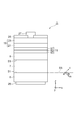
- the LED 1 is a light-emitting diode (nitride-based semiconductor light-emitting element), and includes an n-electrode 29, a substrate 5, an n-type gallium nitride-based semiconductor region 7, a buffer layer 9, and a light-emitting layer that are sequentially provided along a predetermined z-axis direction. 11, a p-type gallium nitride based semiconductor region 19, a p-electrode 25, and a pad electrode 27.
- the substrate 5, the n-type gallium nitride semiconductor region 7, the buffer layer 9, the light emitting layer 11, and the p-type gallium nitride semiconductor region 19 are made of a hexagonal gallium nitride semiconductor.
- the main surface S1 of the substrate 5 extends along a surface perpendicular to the z axis (a surface including the x axis and the y axis).
- the main surface S1 is a reference plane S5 inclined at an inclination angle ⁇ within a range of 63 degrees to 80 degrees or 100 degrees to 117 degrees from a plane orthogonal to the c-axis of the hexagonal gallium nitride semiconductor of the substrate 5. It is a semipolar surface extending along.
- FIG. 1 shows a case where the c-axis is inclined in the m-axis direction as an example.
- the n-type gallium nitride based semiconductor region 7 is provided on the main surface S1, and is in contact with the substrate 5 through the main surface S1.
- the buffer layer 9 is provided between the n-type gallium nitride semiconductor region 7 and the light emitting layer 11 and is in contact with the n-type gallium nitride semiconductor region 7 and the light emitting layer 11 (particularly the barrier layer 13).
- the buffer layer 9 extends along a first axis direction (substantially x-axis direction) that is orthogonal to the interface S3 on the substrate 5 side of the buffer layer 9 and that is shared by the surface including the c-axis and the interface S3. Is larger than the lattice constant of the substrate 5 along the direction of the second axis (substantially x-axis direction) which is perpendicular to the main surface S1 of the substrate 5 and is shared by the surface including the c-axis and the main surface S1. can do.
- the lattice constant of the buffer layer 9 along the direction of the third axis (substantially y-axis direction) orthogonal to the first axis and the c-axis is that of the fourth axis orthogonal to the second axis and the c-axis.
- the lattice constant here is not specific to the substance, but is the lattice constant of the substrate 5 and the buffer layer 9 provided in the LED 1) is there.).
- the buffer layer 9 includes misfit dislocations generated at the interface S3, the misfit dislocations extend in the direction of the third axis, and the density of the misfit dislocations is 5 ⁇ 10 3 cm ⁇ 1 or more and 1 X10 5 cm -1 or less.
- the light emitting layer 11 is provided between the buffer layer 9 and the electron blocking layer 21 between the n-type gallium nitride semiconductor region 7 and the p-type gallium nitride semiconductor region 19. It is in contact with the electron block layer 21.
- the light emitting layer 11 has a single quantum well structure, and includes a barrier layer 13, a well layer 15, and a barrier layer 17 that are sequentially provided on the buffer layer 9 along the z-axis direction.
- the light emitting layer 11 emits light having a peak wavelength in the range of 450 nm to 600 nm.
- the barrier layer 13 is provided between the buffer layer 9 and the well layer 15 and is in contact with the buffer layer 9 and the well layer 15.
- the well layer 15 is provided between the barrier layer 13 and the barrier layer 17 and is in contact with the barrier layer 13 and the barrier layer 17.
- the barrier layer 17 is provided between the well layer 15 and the electron block layer 21 and is in contact with the well layer 15 and the electron block layer 21.
- the difference between the band gap energy of the barrier layers 13 and 17 and the band gap energy of the well layer 15 is 0.7 eV or more.
- the piezoelectric polarization generated in the layer 15 is negative, and the direction of piezoelectric polarization in this case coincides with the direction from the p-type gallium nitride semiconductor region 19 toward the n-type gallium nitride semiconductor region 7.
- the piezo polarization in the well layer 15 is negative, as shown in FIG.
- the height of the barrier with respect to the well layer 15 on the p-type gallium nitride based semiconductor region 19 side is such that the piezo polarization in the well layer 15 is positive. Compared to the case (well structure shown in FIG. 4A) and the case where the piezoelectric polarization in the well layer 15 is zero (well structure shown in FIG. 4B), it is higher. Therefore, in the case of the multiple quantum well structure having a plurality of such wells, the electron injection efficiency into the well layer is lower than in the case of the LED 1 having a single well structure. This effect becomes more remarkable as the height of the barrier with respect to the well on the p-type gallium nitride based semiconductor region 19 side is higher (the emission wavelength is longer).
- the p-type gallium nitride based semiconductor region 19 has an electron block layer 21 and a contact layer 23 that are sequentially provided on the light emitting layer 11 along the z-axis direction.
- the electron blocking layer 21 is provided between the barrier layer 17 and the contact layer 23, and is in contact with the barrier layer 17 and the contact layer 23.
- the p electrode 25 is provided on the p-type gallium nitride based semiconductor region 19 (in particular, the surface of the contact layer 23) and is in contact with the contact layer 23.
- the p electrode 25 is provided with a contact hole penetrating from the surface of the p electrode 25 to the surface of the contact layer 23.
- the pad electrode 27 is provided on the p electrode 25 and is in contact with the p electrode 25.
- the pad electrode 27 is in contact with the contact layer 23 through the contact hole of the p electrode 25.
- the n electrode 29 is provided on the surface of the substrate 5 on the opposite side of the main surface S ⁇ b> 1 and is in contact with
- the substrate 5 is made of GaN having a semipolar main surface S1
- the n-type gallium nitride based semiconductor region 7 is made of n-type doped GaN.
- the thickness of the n-type gallium nitride based semiconductor region 7 is about 2 ⁇ m.
- the buffer layer 9 is made of n-type doped InGaN.
- the In composition ratio of the buffer layer 9 is 0.02, and the Ga composition ratio of the buffer layer 9 is 0.98.
- the thickness of the buffer layer 9 is about 100 nm.
- the barrier layer 13 and the barrier layer 17 are both made of GaN, and the thickness of the barrier layer 13 and the thickness of the barrier layer 17 are both about 15 nm.
- the well layer 15 is made of InGaN, the In composition ratio of the well layer 15 is 0.30, and the Ga composition ratio of the well layer 15 is 0.70.
- the thickness of the well layer 15 is about 3 nm.
- the difference between the band gap energy of the well layer 15 and the band gap energy of the barrier layer 13 and the barrier layer 17 is about 1 eV.
- the electron block layer 21 is made of p-type doped AlGaN, the Al composition ratio of the electron block layer 21 is 0.18, and the Ga composition ratio of the electron block layer 21 is 0.82.
- the thickness of the electron block layer 21 is about 20 nm.
- the contact layer 23 is made of p-type doped GaN, and the contact layer 23 has a thickness of about 50 nm.
- the p electrode 25 is made of Ni / Au
- the pad electrode 27 is made of Ti / Au
- the n electrode 29 is made of Ti / Al.
- a 520 nm band LED structure was fabricated on the substrate 5 having the (20-21) plane corresponding to the plane off by 75 degrees in the m-axis direction as the main surface S1.
- the substrate 5 is held in an atmosphere of NH 3 and H 2 at about 1050 degrees Celsius for about 10 minutes, and after pretreatment (thermal cleaning), the n-type gallium nitride based semiconductor region 7 is set at 1100 degrees Celsius. About 2 ⁇ m was grown.
- the atmospheric temperature was lowered to about 840 degrees Celsius, the buffer layer 9 was grown by about 100 nm, and then the light emitting layer 11 was grown.
- Both the barrier layer 13 and the barrier layer 17 of the light emitting layer 11 were grown by about 15 nm at a growth temperature of about 840 degrees Celsius, and the well layer 15 was grown by about 3 nm at a growth temperature of about 740 degrees Celsius.
- the ambient temperature was raised to about 1000 degrees Celsius, the electron blocking layer 21 was grown about 20 nm, and then the contact layer 23 was grown about 50 nm.
- a p-electrode 25 made of Ni / Au, a pad electrode 27 made of Ti / Au, and an n-electrode 29 made of Ti / Al were deposited.
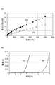
- FIG. 2 is a diagram for explaining the operation of the LED 1.
- the graph indicated by reference symbol G1 in FIG. 2A indicates the light emission output with respect to the drive current in the case of the LED 1 according to the embodiment
- the graph indicated by reference symbol G2 in the drawing indicates light emission with respect to the drive current in the case of other LEDs. Indicates the output.
- the other LED is different from the LED 1 according to the embodiment in the configuration of the light emitting layer and has a multiple quantum well structure including three wells, but the other configuration of the other LED is the embodiment. It is the same as LED1 which concerns on. According to the graphs G1 and G2, it can be seen that the LED 1 according to the example having the single quantum well structure has a higher light emission output than the other LEDs having the multiple quantum well structure.
- the graph indicated by reference sign G3 in FIG. 2B shows the drive current with respect to the drive voltage in the case of the LED 1 according to the embodiment
- the graph indicated by reference sign G4 in the drawing indicates the drive in the case of the other LEDs.
- the drive current with respect to voltage is shown. According to the graphs G3 and G4, it can be seen that the driving voltage of the LED 1 according to the example having the single quantum well structure is lower than that of the other LED having the multiple quantum well structure.
- the main surface S1 of the substrate 5 is in a range of 63 degrees to 80 degrees or 100 degrees to 117 degrees from the plane orthogonal to the c-axis of the hexagonal gallium nitride semiconductor of the substrate 5 Since it extends along the reference plane S5 inclined at the inner inclination angle ⁇ , the piezoelectric polarization generated in the well layer 15 can be reduced as compared with the case where the main surface S1 is orthogonal to the c-axis.
- the well structure of the light emitting layer 11 is distorted in a direction in which carriers (especially electrons) are difficult to escape from the well, and the more wells, the more efficient the injection of carriers (especially electrons) into the wells.
- the well structure of the light emitting layer 11 is a single quantum well structure, the efficiency of carrier (particularly electron) injection into the well layer is improved as compared with the case of the multiple quantum well structure.
- the improvement of the carrier (particularly electron) injection efficiency in the light emitting layer 11 compared with the multiple quantum well structure is that the difference between the band gap energy of the well layer 15 and the band gap energy of the barrier layer 13 and the barrier layer 17 is 0. Since it is 7 eV or more and the difference in band gap energy is relatively large, it becomes more prominent.
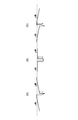
- FIG. 3 shows an outline of the configuration of the LD 31 according to the second embodiment.
- the LD 31 is a laser diode (nitride-based semiconductor light-emitting element), and includes an n-electrode 65, a substrate 33, an n-type gallium nitride-based semiconductor region 35, a guide layer 41, and a light-emitting layer that are sequentially provided along a predetermined z-axis direction. 43, a guide layer 51, a p-type gallium nitride based semiconductor region 53, an insulating film 61, and a p-electrode 63.
- the substrate 33, the n-type gallium nitride semiconductor region 35, the guide layer 41, the light emitting layer 43, the guide layer 51, and the p-type gallium nitride semiconductor region 53 are made of a hexagonal gallium nitride semiconductor.
- the main surface S7 of the substrate 33 extends along a surface perpendicular to the z axis (a surface including the x axis and the y axis).
- the main surface S7 is a reference plane S5 inclined at an inclination angle ⁇ in the range of 63 degrees to 80 degrees or 100 degrees to 117 degrees from the plane orthogonal to the c-axis of the hexagonal gallium nitride semiconductor of the substrate 33. It is a semipolar surface extending along.
- FIG. 3 shows a case where the c-axis is inclined in the m-axis direction as an example.
- the n-type gallium nitride based semiconductor region 35 (particularly, the n-type semiconductor layer 37) is provided on the main surface S7 and is in contact with the substrate 33 through the main surface S7.
- the n-type gallium nitride based semiconductor region 35 includes an n-type semiconductor layer 37 and a cladding layer 39 that are sequentially provided on the main surface S7 of the substrate 33 along the z-axis direction.
- the n-type semiconductor layer 37 is provided between the substrate 33 and the cladding layer 39 and is in contact with the substrate 33 and the cladding layer 39.
- the cladding layer 39 is provided between the n-type semiconductor layer 37 and the guide layer 41, and is in contact with the n-type semiconductor layer 37 and the guide layer 41.
- the relationship between the lattice constant of the cladding layer 39 and the lattice constant of the substrate 33 can be made the same as the relationship between the lattice constant of the buffer layer 9 and the lattice constant of the substrate 5 of the LED 1 according to the first embodiment.
- the cladding layer 39 extends along the direction of the fifth axis (substantially the x-axis direction) that is orthogonal to the interface S9 on the substrate 33 side of the cladding layer 39 and that is shared by the surface including the c-axis and the interface S9.
- the lattice constant is a direction of an axis (this axis is referred to as a second axis as in the first embodiment) shared by a surface that is orthogonal to the main surface S7 of the substrate 33 and includes the c-axis and the main surface S7. It can be made larger than the lattice constant of the substrate 33 along the substantially x-axis direction).
- the lattice constant of the cladding layer 39 along the direction of the sixth axis (substantially y-axis direction) perpendicular to the fifth axis and the c-axis is the axis perpendicular to the second axis and the c-axis (this axis is , which is equal to the lattice constant of the substrate 33 along the direction (substantially the y-axis direction) in the same manner as in the first embodiment (the lattice constant here is not intrinsic to the substance, It is the lattice constant of the substrate 33 and the clad layer 39 in the provided state.)
- the lattice constant since the lattice of the cladding layer 39 is relaxed, the strain is released in the cladding layer 39, and thus the strain generated in the well layer 47 is reduced.
- the clad layer 39 includes misfit dislocations generated at the interface S9, the misfit dislocations extend in the direction of the sixth axis, and the density of the misfit dislocations is 5 ⁇ 10 3 cm ⁇ 1 or more and 1 X10 5 cm -1 or less.
- the guide layer 41 is provided between the n-type gallium nitride based semiconductor region 35 (particularly the clad layer 39) and the light emitting layer 43 (particularly the barrier layer 45), and is in contact with the clad layer 39 and the light emitting layer 43. .
- the relationship between the lattice constant of the guide layer 41 and the lattice constant of the substrate 33 is the same as the relationship between the lattice constant of the buffer layer 9 of the LED 1 and the lattice constant of the substrate 5 according to the first embodiment.
- the light emitting layer 43 has a single quantum well structure, and includes a barrier layer 45, a well layer 47, and a barrier layer 49 that are sequentially provided on the guide layer 41 along the z-axis direction.
- the light emitting layer 43 emits light having a peak wavelength in the range of 450 nm to 600 nm.
- the barrier layer 45 is provided between the guide layer 41 and the well layer 47 and is in contact with the guide layer 41 and the well layer 47.
- the well layer 47 is provided between the barrier layer 45 and the barrier layer 49 and is in contact with the barrier layer 45 and the barrier layer 49.
- the barrier layer 49 is provided between the well layer 47 and the guide layer 51 and is in contact with the well layer 47 and the guide layer 51.
- the guide layer 51 is provided between the light emitting layer 43 (particularly the barrier layer 49) and the p-type gallium nitride based semiconductor region 53 (particularly the electron block layer 55), and is in contact with the barrier layer 49 and the electron block layer 55. ing.
- the difference between the band gap energy of the barrier layer 45 and the barrier layer 49 and the band gap energy of the well layer 47 is 0.7 eV or more.
- the barrier layer 45 and the guide layer 41, and the barrier layer 49 and the guide layer 51 may be under the same conditions, and the guide layer and the barrier layer may be integrated.
- the piezoelectric polarization generated in the layer 47 is negative, and the direction of the piezoelectric polarization in this case coincides with the direction from the p-type gallium nitride semiconductor region 53 toward the n-type gallium nitride semiconductor region 35.
- the piezoelectric polarization in the well layer 47 is negative, as shown in FIG.
- the height of the barrier with respect to the well of the well layer 47 on the p-type gallium nitride based semiconductor region 53 side is the piezoelectric polarization in the well layer 47.
- the piezoelectric polarization in the well layer 47 is higher. Therefore, in the case of the multiple quantum well structure having a plurality of such wells, the electron injection efficiency into the well layer is lower than in the case of the LD 31 having a single well structure. This effect becomes more remarkable as the height of the barrier with respect to the well on the p-type gallium nitride based semiconductor region 53 side is higher (the emission wavelength is longer).
- the p-type gallium nitride based semiconductor region 53 has an electron block layer 55, a cladding layer 57, and a contact layer 59 that are sequentially provided on the guide layer 51 along the z-axis direction.
- the electron blocking layer 55 is provided between the guide layer 51 and the contact layer 59 and is in contact with the guide layer 51 and the contact layer 59.
- the cladding layer 57 is provided between the electron block layer 55 and the contact layer 59 and is in contact with the electron block layer 55 and the contact layer 59.
- the insulating film 61 is provided on the p-type gallium nitride based semiconductor region 53 (particularly, the contact layer 59) and is in contact with the contact layer 59.
- the insulating film 61 is provided with a contact hole penetrating from the surface of the insulating film 61 to the surface of the contact layer 59.
- the p electrode 63 is provided on the insulating film 61 and is in contact with the insulating film 61.
- the p-electrode 63 is in contact with the contact layer 59 through the contact hole of the insulating film 61.
- the n-electrode 65 is provided on the surface of the substrate 33 on the opposite side of the main surface S ⁇ b> 7 and is in contact with the substrate 33.
- the substrate 33 is made of GaN having a semipolar main surface S7, and the n-type semiconductor layer 37 is made of n-type doped GaN.
- the n-type semiconductor layer 37 has a thickness of about 500 nm.
- the clad layer 39 is made of n-type doped InAlGaN.
- the cladding layer 39 has an In composition ratio of 0.02, the cladding layer 39 has an Al composition ratio of 0.09, and the cladding layer 39 has a Ga composition ratio of 0.89.
- the thickness of the cladding layer 39 is about 1.5 ⁇ m.
- the guide layer 41 and the guide layer 51 are both made of InGaN, and the thickness of the guide layer 41 and the thickness of the guide layer 51 are both about 200 nm.
- the In composition ratio of the guide layer 41 and the guide layer 51 is both 0.03, and the Ga composition ratio of the guide layer 41 and the guide layer 51 is 0.97.
- the barrier layer 45 and the barrier layer 49 are both made of GaN, and the thickness of the barrier layer 45 and the thickness of the barrier layer 49 are both about 15 nm.
- the well layer 47 is made of InGaN, and the thickness of the well layer 47 is about 3 nm.
- the In composition ratio of the well layer 47 is 0.30, and the Ga composition ratio of the well layer 47 is 0.70.
- the difference between the band gap energy of the well layer 47 and the band gap energy of the barrier layer 45 and the barrier layer 49 is about 1 eV.
- the electron block layer 55 is made of p-type doped AlGaN.
- the electron block layer 55 has an Al composition ratio of 0.12, and the electron block layer 55 has a Ga composition ratio of 0.88.
- the thickness of the electron block layer 55 is about 20 nm.
- the clad layer 57 is made of p-type doped InAlGaN.
- the In composition ratio of the cladding layer 57 is 0.02, the Al composition ratio of the cladding layer 57 is 0.09, and the Ga composition ratio of the cladding layer 57 is 0.89.
- the thickness of the cladding layer 57 is about 400 nm.
- the contact layer 59 is made of p-type doped GaN.
- the contact layer 59 has a thickness of about 50 nm.
- the insulating film 61 is made of, for example, SiO 2 .
- the p-electrode 63 is composed of Ni / Au and a pad electrode made of Ti / Au provided on the Ni / Au surface.
- the n-electrode 65 is composed of Ti / Al and a pad electrode made of Ti / Au provided on the Ti / Al surface.
- An LD structure of a 520 nm band was fabricated on the substrate 33 having a (20-21) plane corresponding to a plane off by 75 degrees in the m-axis direction as a main surface S7.
- the substrate 33 is held in an atmosphere of NH 3 and H 2 at about 1050 degrees Celsius for about 10 minutes, and after pretreatment (thermal cleaning), the n-type semiconductor layer 37 is 500 nm at about 1050 degrees Celsius. It was grown only to the extent.
- the ambient temperature was lowered to about 840 degrees Celsius, and the cladding layer 39 was grown by about 1.5 ⁇ m.
- the guide layer 41, the light emitting layer 43, and the guide layer 51 were sequentially grown.
- the guide layer 41 and the guide layer 51 are both grown by about 200 nm at a growth temperature of about 840 degrees Celsius, and the barrier layer 45 and the barrier layer 49 are both grown by about 15 nm at a growth temperature of about 840 degrees Celsius,
- the well layer 47 was grown by about 3 nm at a growth temperature of about 740 degrees Celsius.
- the ambient temperature was raised to about 1000 degrees Celsius
- the electron block layer 55 was grown by about 20 nm.
- the atmospheric temperature was lowered again to about 840 degrees Celsius, and the cladding layer 57 was grown by about 400 nm. Further, at this temperature, the contact layer 59 was also grown by about 50 nm.
- an insulating film 61 was formed, and a stripe window having a width of about 10 ⁇ m was formed by wet etching. Thereafter, a p-electrode 63 made of Ni / Au and Ti / Au pad electrodes and an n-electrode 65 made of Ti / Al and Ti / Au pad electrodes were deposited.
- the substrate 33 and the n-type gallium nitride based semiconductor region 35, the guide layer 41, the light emitting layer 43, the guide layer 51, and the p-type gallium nitride based semiconductor region 53 grown on the substrate 33 are about 800 ⁇ m. Cleavage was performed at intervals, and a dielectric multilayer film composed of SiO 2 / TiO 2 was formed on the cleaved surface, thereby producing a gain guide type laser.
- a comparative example of the LD 31 according to the example another LD (referred to as a first comparative example LD) having a light emitting layer having a multiple quantum well structure including three wells was manufactured.
- Other configurations of the first comparative example LD are the same as the configurations of the LD 31 according to the example except for the configuration of the light emitting layer.
- the first comparative example LD was energized with a pulse width of 500 nsec and a duty of 0.1%.
- the threshold current of the LD 31 according to the example was 800 mA, but the threshold current of the first comparative example LD was 1100 mA.
- the oscillation wavelength of both the LD 31 according to the example and the first comparative example LD was 520 nm.
- the LD 31 according to the example has only one InGaN well layer (well layer 47) having a high refractive index, light confinement is slightly disadvantageous as compared with the first comparative example LD, but the luminous efficiency is improved. It is considered that the improvement of the carrier density per unit well contributed to the lower threshold.
- a single well structure LD in which the guide layer is InGaN (the composition ratio of In is 0.01 and the composition ratio of Ga is 0.99) ( 2nd comparative example LD) was produced.
- Other configurations of the second comparative example LD are the same as those of the LD 31 according to the example except for the configuration of the guide layer.
- a misfit dislocation of 2 ⁇ 10 4 cm ⁇ 1 was observed at the interface S11 between the guide layer 41 and the cladding layer 39 on the n side. Misfit dislocations were not observed in the well layer 47.
- the n-side guide layer (made of InGaN having an In composition ratio of 0.01 and Ga composition ratio of 0.99) and a cladding layer (similar to the cladding layer 39)
- the light emitting layer (same structure as the light emitting layer 43)
- no well layer (same structure as the well layer 47)
- barrier layer (similar to the barrier layers 45 and 49) were found.
- the defects penetrating from the interface to the surface of the contact layer occurred at a density of 1 ⁇ 10 8 cm ⁇ 2 .
- the guide layer 41 relaxes the strain, it is considered that the generation of defects in the light emitting layer 43 is suppressed even in the well layer 47 having a long wavelength and a high In composition ratio. It is done. Further, when the second comparative example LD was energized, it did not oscillate. The reason for this is considered that the light confinement efficiency is lowered due to a decrease in light emission efficiency due to generation of defects in the light emitting layer and a low In composition ratio in the guide layer.
- the main surface S7 of the substrate 33 is in a range of 63 degrees to 80 degrees or 100 degrees to 117 degrees from the plane orthogonal to the c-axis of the hexagonal gallium nitride semiconductor of the substrate 33. Since it extends along the reference plane S5 inclined at the inner inclination angle ⁇ , the piezoelectric polarization generated in the well layer 47 can be reduced as compared with the case where the main surface S7 is orthogonal to the c-axis.
- the well structure of the light emitting layer 43 is distorted in a direction in which carriers (especially electrons) are difficult to escape from the well, and the more wells, the more efficient the injection of carriers (especially electrons) into the wells.
- the well structure of the light emitting layer 43 is a single quantum well structure, the efficiency of injecting carriers (particularly electrons) into the well layer is improved as compared with the case of the multiple quantum well structure.
- the improvement in the injection efficiency of electron carriers (especially electrons) in the light emitting layer 43 compared with the multiple quantum well structure is that the difference between the band gap energy of the well layer 47 and the band gap energy of the barrier layer 45 and the barrier layer 49 is as follows.
- the light emitting layer 43 is provided on the guide layer 41 in a coherent manner after lattice relaxation of the guide layer 41 provided on the main surface S7 only in a direction along the first axis (a direction parallel to the off-state). Therefore, the distortion of the well layer 47 of the light emitting layer 43 is alleviated, and the piezo polarization can be further reduced. In addition, even in a situation where the In composition of the well layer 47 is high and the lattice mismatch between the barrier layer 45 and the barrier layer 49 is large, generation of defects in the well layer can be suppressed. Since misfit dislocations exist at the interface S11 of the guide layer 41, the influence of the misfit dislocations on the characteristics of the LD 31 is relatively small.
- the LED 1 according to the example of the first embodiment (the LED 1 according to the example is referred to as an example LED in the following for the sake of simplicity) will be further described.
- This example LED has a single quantum well structure as described above.
- a comparative example of the example LED another LED (referred to as a first comparative example LED) having a light emitting layer having a multiple quantum well structure including three wells was produced.
- the configuration of the first comparative example LED was the same as that of the example LED except that it had a light emitting layer having a multiple quantum well structure.
- the first comparative example LED had a configuration in which an epitaxial layer including a light emitting layer was provided on a surface of a hexagonal gallium nitride semiconductor that was turned off by 75 degrees in the m-axis direction.
- a single quantum well structure having a single quantum well layer is referred to as SQW
- a multiple quantum well structure including three quantum well layers is referred to as 3QW.
- the evaluation results are shown in FIG.
- the graph indicated by reference sign G5 in FIG. 5 shows the measurement results for the example LED
- the graph indicated by reference sign G6 in FIG. 5 shows the measurement results for the first comparative example LED.
- the PL characteristics shown in FIG. 5 were excited by an ArSHG laser (wavelength 244 nm), and carriers were excited throughout the epitaxial layer. That is, regardless of the number of well layers included in the light-emitting layer (whether it is a single quantum well layer of SQW or three quantum well layers of 3QW), the excited carrier density is considered to be substantially the same. .
- the temperature when the temperature is lowered, the non-luminescent process is suppressed and the PL intensity is improved.
- the PL intensity of both the example LED and the first comparative example LED was substantially equal. This means that the luminous efficiency of the light emitting layers of both the example LED and the first comparative example LED is equal.
- the temperature dependence of the EL characteristics of the example LED (SQW) and the first comparative example LED (3QW) was also evaluated.
- the evaluation results are shown in FIG.
- the graph indicated by reference numeral G7 in FIG. 6 shows the measurement results for the example LED
- the graph indicated by reference numeral G8 in FIG. 6 shows the measurement results for the first comparative example LED.
- the EL characteristics shown in FIG. 6 are measurement results measured at a current value of 2 mA.
- the EL intensity of the example LED (SQW) exceeded the EL intensity of the first comparative example LED over the entire temperature range (temperature range of 500 K or less) shown in FIG.
- the example LED and the first comparative example LED had substantially the same PL intensity, but a difference was observed in the EL intensity of the example LED and the first comparative example LED.
- the difference in EL intensity between the example LED and the first comparative example LED indicates that the carrier injection efficiency of the example LED and the first comparative example LED is different. Yes. From the above, it was found that the injection of carriers was improved in the SQW example LED compared to the 3QW first comparative example LED.
- a comparative example of the example LED another LED (referred to as a second comparative example LED) having a 3QW light emitting layer provided on the c-plane of a hexagonal gallium nitride semiconductor GaN substrate was further prepared.
- the configuration of the second comparative example LED is the same as that of the first comparative example LED except that an epi layer including a light emitting layer is provided on the c-plane of a GaN substrate of a hexagonal gallium nitride semiconductor.
- the PL of each of the example LED, the first comparative example LED, and the second comparative example LED due to bias application was evaluated at a temperature of 100 K, and the relationship between the direction of piezoelectric polarization and carrier injection was measured.
- FIG. 7 shows measurement results of the applied voltage dependence of the PL wavelength of each of the example LED, the first comparative example LED, and the second comparative example LED.
- the graph indicated by reference numeral G9 in FIG. 7 shows the measurement results for the example LED
- the graph indicated by reference numeral G10 in FIG. 7 indicates the measurement results for the first comparative example LED
- the graph indicated by reference numeral G11 in FIG. Shows the measurement results for the second comparative LED.
- the PL wavelength is red-shifted in the case of the second comparative example LED, whereas in the case of the example LED and the first comparative example LED. It can be seen that the PL wavelength is blue shifted.
- the PL wavelength measurement result corresponds to the fact that the piezo polarization of the well layer is “positive” in the case of the second comparative example LED and “negative” in the case of the example LED and the first comparative example LED. is doing.
- FIG. 8 also shows the measurement results of the applied voltage dependence of the PL intensity of each of the example LED, the first comparative example LED, and the second comparative example LED.
- the graph indicated by reference sign G12 in FIG. 8 shows the measurement results for the example LED
- the graph indicated by reference sign G13 in FIG. 8 indicates the measurement result for the first comparative example LED
- the graph indicated by reference sign G14 in FIG. Shows the measurement results for the second comparative LED.
- the height of the n-side wall with respect to the electron E1 (the height of the n-side wall of the well layer Q1 is a relative value V2 with respect to the energy level V1 in the well layer Q1.
- V2 the height of the p-side wall relative to the electron E1
- V3 the relative value V3 to the energy level V1 in the well layer Q1
- the piezoelectric polarization of the well layer is “negative” and the band is bent as shown in FIG. 9B, the electrons E1 trapped in the well layer Q2 included in this band are likely to escape to the n side.
- the height of the n-side wall with respect to the electron E1 (the height of the n-side wall of the well layer Q2 is a relative value V5 with respect to the energy level V4 in the well layer Q2.
- the PL intensity decreased when the applied voltage was relatively small.
- the PL intensity was extremely lowered because the electrons that once escaped to the n side are not trapped again in the next well layer adjacent thereto.
- the first comparative example LED has a configuration in which an epitaxial layer including a light emitting layer is provided on a surface of a hexagonal gallium nitride semiconductor that is off by 75 degrees in the m-axis direction, and there are a plurality of well layers. Therefore, the injection electron density of each well layer becomes non-uniform. Therefore, the SQW example LED is more effective in improving the light emission efficiency and voltage than the first comparative example LED.
- the direction of piezo polarization in the well layer was determined using the bias application PL.
- the bias application PL is a measurement in which PL is detected by irradiating excitation light from above the Ni / Au electrode (p electrode 25, etc.) while applying an external voltage to the example LED and the first and second comparative example LEDs. .
- the piezoelectric polarization of the well layer is strong to “positive”, the energy gap V7 shown in FIG. 10 (A) is smaller than the energy gap V7 as shown in FIG.
- the energy gap V8 (energy gap V7> energy gap V8) is reduced, and a red shift is observed. Therefore, when a red shift is observed by applying a forward bias, it can be determined that the piezo polarization of the well layer is “positive”.
- the piezo polarization of the well layer is strong “negative”, the energy gap V9 shown in FIG. 11A becomes larger than the energy gap V9 as shown in FIG. Since the energy gap V10 increases to a large value (energy gap V9 ⁇ energy gap V10), a blue shift is observed. Therefore, when a blue shift is observed by applying a forward bias, the piezo polarization of the well layer can be determined to be “negative”.
- an LED including an SQW light-emitting layer provided on the c-plane of the sapphire substrate (emitting light of a wavelength of 470 nm band and referred to as a third comparative LED) and an epitaxial including a 3QW light-emitting layer A layer is produced with an LED (emitting light having a wavelength of 470 nm band and called a fourth comparative example LED) provided on the c-plane of the sapphire substrate, and for each of the third and fourth comparative example LEDs and the example LED CL observation (CL: cathode luminescence) was performed.
- FIG. 12 shows the observation results of the CL observation performed on the third comparative example LED
- FIG. 13 shows the observation results of the CL observation performed on the fourth comparative example LED.
- FIG. 14 shows the observation results of the CL observation performed on the example LED.
- the light emission is relatively uniform.
- the CL observation for the third comparative example LED of the SQW In the observation results observation results shown in FIG. 12
- a non-light-emitting region was observed.
- the strain distribution in the c-plane becomes non-uniform, and the non-light emitting region increases. For this reason, it is considered that a non-light emitting region was observed in the third comparative example LED of SQW.
- the embodiment LED is an LED having a configuration in which an epitaxial layer including a light emitting layer of SQW is provided on a surface of a hexagonal gallium nitride semiconductor, which is off 75 degrees in the m-axis direction, as described above.
- the light emission is relatively uniform because the crystal structure of the InGaN well layer formed on the surface of the crystalline gallium nitride semiconductor that is 75 degrees off in the m-axis direction is relatively high. It is thought that there was.
- the effect of SQW according to the example of the first embodiment is particularly great in the plane orientation and the growth conditions that enable uniform growth of the InGaN well layer.
- the substrate main surface is inclined from the plane orthogonal to the c-axis in the range of 63 ° to 80 ° or 100 ° to 117 °, In is easily taken in, and the uniformity of the InGaN well layer is excellent. Become.
- an object of the present embodiment is to provide a nitride-based semiconductor light-emitting device with improved carrier injection efficiency into a well layer.
Abstract
Description
図1に、第1の実施形態に係るLED1の構成の概略を示す。LED1は、発光ダイオード(窒化物系半導体発光素子)であり、所定のz軸方向に沿って順次設けられたn電極29、基板5、n型窒化ガリウム系半導体領域7、緩衝層9、発光層11、p型窒化ガリウム系半導体領域19、p電極25及びパッド電極27を備える。基板5、n型窒化ガリウム系半導体領域7、緩衝層9、発光層11及びp型窒化ガリウム系半導体領域19は、六方晶系窒化ガリウム系半導体からなる。基板5の主面S1は、z軸に垂直な面(x軸及びy軸を含む面)に沿って延びている。主面S1は、基板5の六方晶系窒化ガリウム系半導体のc軸に直交する面から63度以上80度以下または100度以上117度以下の範囲内の傾斜角θで傾斜した基準平面S5に沿って延びている半極性面である。図1には、一例としてc軸がm軸方向に傾斜した場合を示してある。
図3に、第2の実施形態に係るLD31の構成の概略を示す。LD31は、レーザダイオード(窒化物系半導体発光素子)であり、所定のz軸方向に沿って順次設けられたn電極65、基板33、n型窒化ガリウム系半導体領域35、ガイド層41、発光層43、ガイド層51、p型窒化ガリウム系半導体領域53、絶縁膜61及びp電極63を備える。基板33、n型窒化ガリウム系半導体領域35、ガイド層41、発光層43、ガイド層51、p型窒化ガリウム系半導体領域53は、六方晶系窒化ガリウム系半導体からなる。基板33の主面S7は、z軸に垂直な面(x軸及びy軸を含む面)に沿って延びている。主面S7は、基板33の六方晶系窒化ガリウム系半導体のc軸に直交する面から63度以上80度以下または100度以上117度以下の範囲内の傾斜角θで傾斜した基準平面S5に沿って延びている半極性面である。図3には、一例としてc軸がm軸方向に傾斜した場合を示してある。
Claims (8)
- 窒化物系半導体発光素子であって、
六方晶系窒化ガリウム系半導体からなる基板と、
前記基板の主面に設けられたn型窒化ガリウム系半導体領域と、
前記n型窒化ガリウム系半導体領域上に設けられた単一量子井戸構造の発光層と、
前記発光層上に設けられたp型窒化ガリウム系半導体領域と
を備え、
前記発光層は、前記n型窒化ガリウム系半導体領域と前記p型窒化ガリウム系半導体領域との間に設けられており、
前記発光層は、井戸層及び障壁層を含み、
前記井戸層は、InGaNであり、
前記主面は、前記六方晶系窒化ガリウム系半導体のc軸方向に直交する面から63度以上80度以下または100度以上117度以下の範囲内の傾斜角で傾斜した基準平面に沿って延びている、
ことを特徴とする窒化物系半導体発光素子。 - 前記井戸層に生じるピエゾ分極の向きは、前記p型窒化ガリウム系半導体領域から前記n型窒化ガリウム系半導体領域に向かう方向と一致する、ことを特徴とする請求項1に記載の窒化物系半導体発光素子。
- 前記障壁層のバンドギャップエネルギーと前記井戸層のバンドギャップエネルギーとの差は0.7eV以上である、ことを特徴とする請求項1又は請求項2に記載の窒化物系半導体発光素子。
- 前記発光層は、450nm以上600nm以下の範囲内にあるピーク波長の光を発光する、ことを特徴とする請求項1~請求項3の何れか一項に記載の窒化物系半導体発光素子。
- InGaN層を更に備え、
前記InGaN層は、前記n型窒化ガリウム系半導体領域と前記発光層との間に設けられ、
前記InGaN層の前記基板側の第1の界面に直交し前記c軸を含む面と前記第1の界面とが共有する第1の軸の方向に沿った前記InGaN層の格子定数は、前記主面に直交し前記c軸を含む面と前記主面とが共有する第2の軸の方向に沿った前記基板の格子定数よりも大きく、前記第1の軸と前記c軸とに直交する第3の軸の方向に沿った前記InGaN層の格子定数は、前記第2の軸と前記c軸とに直交する第4の軸の方向に沿った前記基板の格子定数に等しい、ことを特徴とする請求項1~請求項4の何れか一項に記載の窒化物系半導体発光素子。 - 前記InGaN層は前記第1の界面に生じたミスフィット転位を含み、当該ミスフィット転位は前記第3の軸の方向に延びており、当該ミスフィット転位の密度は5×103cm-1以上1×105cm-1以下の範囲内にある、ことを特徴とする請求項5に記載の窒化物系半導体発光素子。
- 前記n型窒化ガリウム系半導体領域はn型のInAlGaN層を含み、
前記InAlGaN層の前記基板側の第2の界面に直交し前記c軸を含む面と前記第2の界面とが共有する第5の軸の方向に沿った前記InAlGaN層の格子定数は、前記第2の軸の方向に沿った前記基板の格子定数よりも大きく、前記第5の軸と前記c軸とに直交する第6の軸の方向に沿った前記InAlGaN層の格子定数は、前記第4の軸の方向に沿った前記基板の格子定数に等しい、ことを特徴とする請求項1~請求項5の何れか一項に記載の窒化物系半導体発光素子。 - 前記InAlGaN層は前記第2の界面に生じたミスフィット転位を含み、当該ミスフィット転位は前記第6の軸の方向に延びており、当該ミスフィット転位の密度は5×103cm-1以上1×105cm-1以下の範囲内にある、ことを特徴とする請求項7に記載の窒化物系半導体発光素子。
Priority Applications (3)
| Application Number | Priority Date | Filing Date | Title |
|---|---|---|---|
| CN2010800018062A CN102099935B (zh) | 2009-07-15 | 2010-06-14 | 氮化物类半导体发光元件 |
| EP10787665.8A EP2455988A4 (en) | 2009-07-15 | 2010-06-14 | NITRIDE-BASED SEMICONDUCTOR LIGHT EMITTING ELEMENT |
| US12/999,987 US8405066B2 (en) | 2009-07-15 | 2010-06-14 | Nitride-based semiconductor light-emitting device |
Applications Claiming Priority (4)
| Application Number | Priority Date | Filing Date | Title |
|---|---|---|---|
| JP2009-166923 | 2009-07-15 | ||
| JP2009166923 | 2009-07-15 | ||
| JP2010-021307 | 2010-02-02 | ||
| JP2010021307A JP5234022B2 (ja) | 2009-07-15 | 2010-02-02 | 窒化物系半導体発光素子 |
Publications (1)
| Publication Number | Publication Date |
|---|---|
| WO2011007637A1 true WO2011007637A1 (ja) | 2011-01-20 |
Family
ID=43449247
Family Applications (1)
| Application Number | Title | Priority Date | Filing Date |
|---|---|---|---|
| PCT/JP2010/060054 WO2011007637A1 (ja) | 2009-07-15 | 2010-06-14 | 窒化物系半導体発光素子 |
Country Status (7)
| Country | Link |
|---|---|
| US (1) | US8405066B2 (ja) |
| EP (1) | EP2455988A4 (ja) |
| JP (1) | JP5234022B2 (ja) |
| KR (1) | KR101213860B1 (ja) |
| CN (1) | CN102099935B (ja) |
| TW (1) | TW201121095A (ja) |
| WO (1) | WO2011007637A1 (ja) |
Cited By (3)
| Publication number | Priority date | Publication date | Assignee | Title |
|---|---|---|---|---|
| CN102185056A (zh) * | 2011-05-05 | 2011-09-14 | 中国科学院半导体研究所 | 提高电子注入效率的氮化镓基发光二极管 |
| US20120230359A1 (en) * | 2011-03-07 | 2012-09-13 | Sumitomo Electric Industries, Ltd. | Quantum cascade laser |
| WO2013128894A1 (ja) * | 2012-02-27 | 2013-09-06 | 国立大学法人山口大学 | 半導体発光素子 |
Families Citing this family (2)
| Publication number | Priority date | Publication date | Assignee | Title |
|---|---|---|---|---|
| JP6438542B1 (ja) * | 2017-07-27 | 2018-12-12 | 日機装株式会社 | 半導体発光素子 |
| CN114497303B (zh) * | 2022-04-14 | 2022-06-24 | 江苏第三代半导体研究院有限公司 | 长波长led同质外延结构、其制备方法及应用 |
Citations (5)
| Publication number | Priority date | Publication date | Assignee | Title |
|---|---|---|---|---|
| JP2003347585A (ja) * | 2002-03-19 | 2003-12-05 | Nobuhiko Sawaki | 半導体発光素子およびその製造方法 |
| JP2007134507A (ja) * | 2005-11-10 | 2007-05-31 | Sumitomo Electric Ind Ltd | 半導体発光素子、および半導体発光素子を作製する方法 |
| JP2008060375A (ja) * | 2006-08-31 | 2008-03-13 | Sanyo Electric Co Ltd | 窒化物系半導体発光素子の製造方法および窒化物系半導体発光素子 |
| JP2009088230A (ja) * | 2007-09-28 | 2009-04-23 | Furukawa Electric Co Ltd:The | 半導体発光素子およびその製造方法 |
| JP4475358B1 (ja) * | 2008-08-04 | 2010-06-09 | 住友電気工業株式会社 | GaN系半導体光素子、GaN系半導体光素子を作製する方法、及びエピタキシャルウエハ |
Family Cites Families (15)
| Publication number | Priority date | Publication date | Assignee | Title |
|---|---|---|---|---|
| JP2780691B2 (ja) | 1994-12-02 | 1998-07-30 | 日亜化学工業株式会社 | 窒化物半導体発光素子 |
| US6072197A (en) * | 1996-02-23 | 2000-06-06 | Fujitsu Limited | Semiconductor light emitting device with an active layer made of semiconductor having uniaxial anisotropy |
| JP4010318B2 (ja) * | 1996-03-22 | 2007-11-21 | 住友化学株式会社 | 発光素子 |
| WO2000016455A1 (fr) * | 1998-09-10 | 2000-03-23 | Rohm Co., Ltd. | Element lumineux semi-conducteur et laser a semi-conducteur |
| US7315050B2 (en) * | 2001-05-28 | 2008-01-01 | Showa Denko K.K. | Semiconductor device, semiconductor layer and production method thereof |
| US7045808B2 (en) * | 2003-12-26 | 2006-05-16 | Hitachi Cable, Ltd. | III-V nitride semiconductor substrate and its production lot, and III-V nitride semiconductor device and its production method |
| KR100568299B1 (ko) * | 2004-03-31 | 2006-04-05 | 삼성전기주식회사 | 질화갈륨계 반도체 발광소자 |
| US20070221932A1 (en) * | 2006-03-22 | 2007-09-27 | Sanyo Electric Co., Ltd. | Method of fabricating nitride-based semiconductor light-emitting device and nitride-based semiconductor light-emitting device |
| JP5286723B2 (ja) | 2007-09-14 | 2013-09-11 | 国立大学法人京都大学 | 窒化物半導体レーザ素子 |
| JP5003527B2 (ja) * | 2008-02-22 | 2012-08-15 | 住友電気工業株式会社 | Iii族窒化物発光素子、及びiii族窒化物系半導体発光素子を作製する方法 |
| US20090310640A1 (en) * | 2008-04-04 | 2009-12-17 | The Regents Of The University Of California | MOCVD GROWTH TECHNIQUE FOR PLANAR SEMIPOLAR (Al, In, Ga, B)N BASED LIGHT EMITTING DIODES |
| US7919764B2 (en) * | 2008-05-06 | 2011-04-05 | The United States Of America As Represented By The Secretary Of The Army | Method and apparatus for enhanced terahertz radiation from high stacking fault density |
| JP4375497B1 (ja) * | 2009-03-11 | 2009-12-02 | 住友電気工業株式会社 | Iii族窒化物半導体素子、エピタキシャル基板、及びiii族窒化物半導体素子を作製する方法 |
| EP2543119B1 (en) * | 2010-03-04 | 2020-02-12 | The Regents of The University of California | Semi-polar iii-nitride optoelectronic devices on m-plane gan substrates with miscuts in the ranges 1 to 15 degrees or -1 to -15 degrees in the c-direction |
| US8761218B2 (en) * | 2010-04-05 | 2014-06-24 | The Regents Of The University Of California | Aluminum gallium nitride barriers and separate confinement heterostructure (SCH) layers for semipolar plane III-nitride semiconductor-based light emitting diodes and laser diodes |
-
2010
- 2010-02-02 JP JP2010021307A patent/JP5234022B2/ja active Active
- 2010-06-14 US US12/999,987 patent/US8405066B2/en active Active
- 2010-06-14 KR KR1020107027739A patent/KR101213860B1/ko not_active IP Right Cessation
- 2010-06-14 CN CN2010800018062A patent/CN102099935B/zh not_active Expired - Fee Related
- 2010-06-14 EP EP10787665.8A patent/EP2455988A4/en not_active Withdrawn
- 2010-06-14 WO PCT/JP2010/060054 patent/WO2011007637A1/ja active Application Filing
- 2010-06-29 TW TW099121312A patent/TW201121095A/zh unknown
Patent Citations (5)
| Publication number | Priority date | Publication date | Assignee | Title |
|---|---|---|---|---|
| JP2003347585A (ja) * | 2002-03-19 | 2003-12-05 | Nobuhiko Sawaki | 半導体発光素子およびその製造方法 |
| JP2007134507A (ja) * | 2005-11-10 | 2007-05-31 | Sumitomo Electric Ind Ltd | 半導体発光素子、および半導体発光素子を作製する方法 |
| JP2008060375A (ja) * | 2006-08-31 | 2008-03-13 | Sanyo Electric Co Ltd | 窒化物系半導体発光素子の製造方法および窒化物系半導体発光素子 |
| JP2009088230A (ja) * | 2007-09-28 | 2009-04-23 | Furukawa Electric Co Ltd:The | 半導体発光素子およびその製造方法 |
| JP4475358B1 (ja) * | 2008-08-04 | 2010-06-09 | 住友電気工業株式会社 | GaN系半導体光素子、GaN系半導体光素子を作製する方法、及びエピタキシャルウエハ |
Non-Patent Citations (1)
| Title |
|---|
| See also references of EP2455988A4 * |
Cited By (6)
| Publication number | Priority date | Publication date | Assignee | Title |
|---|---|---|---|---|
| US20120230359A1 (en) * | 2011-03-07 | 2012-09-13 | Sumitomo Electric Industries, Ltd. | Quantum cascade laser |
| US8817835B2 (en) * | 2011-03-07 | 2014-08-26 | Sumitomo Electric Industries, Ltd. | Quantum cascade laser |
| CN102185056A (zh) * | 2011-05-05 | 2011-09-14 | 中国科学院半导体研究所 | 提高电子注入效率的氮化镓基发光二极管 |
| CN102185056B (zh) * | 2011-05-05 | 2012-10-03 | 中国科学院半导体研究所 | 提高电子注入效率的氮化镓基发光二极管 |
| WO2013128894A1 (ja) * | 2012-02-27 | 2013-09-06 | 国立大学法人山口大学 | 半導体発光素子 |
| JPWO2013128894A1 (ja) * | 2012-02-27 | 2015-07-30 | 国立大学法人山口大学 | 半導体発光素子 |
Also Published As
| Publication number | Publication date |
|---|---|
| CN102099935B (zh) | 2013-06-26 |
| EP2455988A1 (en) | 2012-05-23 |
| JP5234022B2 (ja) | 2013-07-10 |
| US20110227035A1 (en) | 2011-09-22 |
| KR101213860B1 (ko) | 2012-12-18 |
| JP2011040709A (ja) | 2011-02-24 |
| CN102099935A (zh) | 2011-06-15 |
| KR20110020246A (ko) | 2011-03-02 |
| EP2455988A4 (en) | 2014-03-12 |
| US8405066B2 (en) | 2013-03-26 |
| TW201121095A (en) | 2011-06-16 |
Similar Documents
| Publication | Publication Date | Title |
|---|---|---|
| JP4924185B2 (ja) | 窒化物半導体発光素子 | |
| WO2013084926A1 (ja) | 窒化物半導体発光素子およびその製造方法 | |
| JP5087540B2 (ja) | 窒化物半導体発光素子 | |
| JP4775455B2 (ja) | Iii族窒化物半導体レーザ、及びiii族窒化物半導体レーザを作製する方法 | |
| WO2011077473A1 (ja) | 窒化物半導体発光素子およびその製造方法 | |
| US20110212560A1 (en) | Method for fabricating nitride semiconductor light emitting device and method for fabricating epitaxial wafer | |
| JP4074290B2 (ja) | 半導体発光素子及びその製造方法 | |
| US8803274B2 (en) | Nitride-based semiconductor light-emitting element | |
| JPWO2007138658A1 (ja) | 窒化物半導体発光素子 | |
| WO2013002389A1 (ja) | Iii族窒化物半導体素子、及び、iii族窒化物半導体素子の製造方法 | |
| JP5234022B2 (ja) | 窒化物系半導体発光素子 | |
| JP5522147B2 (ja) | 窒化物半導体発光素子、及び、窒化物半導体発光素子の作製方法 | |
| JP5252042B2 (ja) | Iii族窒化物半導体発光素子、及びiii族窒化物半導体発光素子を作製する方法 | |
| JP2009245982A (ja) | 窒化物発光素子 | |
| JP2009259864A (ja) | Iii族窒化物半導体レーザ | |
| JP5733295B2 (ja) | 窒化物半導体発光素子、窒化物半導体発光素子を作製する方法 | |
| JP6115092B2 (ja) | 半導体発光装置及び半導体発光装置の製造方法 | |
| KR101161970B1 (ko) | Ⅲ족 질화물 반도체 레이저 다이오드 | |
| JP5379216B2 (ja) | Iii族窒化物半導体レーザ | |
| WO2014127136A1 (en) | High power blue-violet iii-nitride semipolar laser diodes | |
| JP2011188000A (ja) | Iii族窒化物半導体レーザ、及びiii族窒化物半導体レーザを作製する方法 | |
| JPWO2005022711A1 (ja) | 窒化物半導体発光素子およびその製造方法 | |
| JP2014078763A (ja) | 窒化物半導体発光素子、及び、窒化物半導体発光素子の作製方法 |
Legal Events
| Date | Code | Title | Description |
|---|---|---|---|
| WWE | Wipo information: entry into national phase |
Ref document number: 201080001806.2 Country of ref document: CN |
|
| ENP | Entry into the national phase |
Ref document number: 20107027739 Country of ref document: KR Kind code of ref document: A |
|
| WWE | Wipo information: entry into national phase |
Ref document number: 12999987 Country of ref document: US |
|
| WWE | Wipo information: entry into national phase |
Ref document number: 2010787665 Country of ref document: EP |
|
| 121 | Ep: the epo has been informed by wipo that ep was designated in this application |
Ref document number: 10787665 Country of ref document: EP Kind code of ref document: A1 |
|
| NENP | Non-entry into the national phase |
Ref country code: DE |