WO2010150487A1 - 半導体封止用樹脂組成物、及び半導体装置 - Google Patents
半導体封止用樹脂組成物、及び半導体装置 Download PDFInfo
- Publication number
- WO2010150487A1 WO2010150487A1 PCT/JP2010/003990 JP2010003990W WO2010150487A1 WO 2010150487 A1 WO2010150487 A1 WO 2010150487A1 JP 2010003990 W JP2010003990 W JP 2010003990W WO 2010150487 A1 WO2010150487 A1 WO 2010150487A1
- Authority
- WO
- WIPO (PCT)
- Prior art keywords
- group
- resin composition
- resin
- phenol resin
- semiconductor
- Prior art date
- Legal status (The legal status is an assumption and is not a legal conclusion. Google has not performed a legal analysis and makes no representation as to the accuracy of the status listed.)
- Ceased
Links
- 0 *c(cc(cc1)O)c1O Chemical compound *c(cc(cc1)O)c1O 0.000 description 2
Images



Classifications
-
- C—CHEMISTRY; METALLURGY
- C08—ORGANIC MACROMOLECULAR COMPOUNDS; THEIR PREPARATION OR CHEMICAL WORKING-UP; COMPOSITIONS BASED THEREON
- C08G—MACROMOLECULAR COMPOUNDS OBTAINED OTHERWISE THAN BY REACTIONS ONLY INVOLVING UNSATURATED CARBON-TO-CARBON BONDS
- C08G59/00—Polycondensates containing more than one epoxy group per molecule; Macromolecules obtained by polymerising compounds containing more than one epoxy group per molecule using curing agents or catalysts which react with the epoxy groups
- C08G59/18—Macromolecules obtained by polymerising compounds containing more than one epoxy group per molecule using curing agents or catalysts which react with the epoxy groups ; e.g. general methods of curing
- C08G59/40—Macromolecules obtained by polymerising compounds containing more than one epoxy group per molecule using curing agents or catalysts which react with the epoxy groups ; e.g. general methods of curing characterised by the curing agents used
- C08G59/62—Alcohols or phenols
-
- H—ELECTRICITY
- H10—SEMICONDUCTOR DEVICES; ELECTRIC SOLID-STATE DEVICES NOT OTHERWISE PROVIDED FOR
- H10W—GENERIC PACKAGES, INTERCONNECTIONS, CONNECTORS OR OTHER CONSTRUCTIONAL DETAILS OF DEVICES COVERED BY CLASS H10
- H10W74/00—Encapsulations, e.g. protective coatings
- H10W74/40—Encapsulations, e.g. protective coatings characterised by their materials
- H10W74/47—Encapsulations, e.g. protective coatings characterised by their materials comprising organic materials, e.g. plastics or resins
- H10W74/473—Encapsulations, e.g. protective coatings characterised by their materials comprising organic materials, e.g. plastics or resins containing a filler
-
- C—CHEMISTRY; METALLURGY
- C08—ORGANIC MACROMOLECULAR COMPOUNDS; THEIR PREPARATION OR CHEMICAL WORKING-UP; COMPOSITIONS BASED THEREON
- C08G—MACROMOLECULAR COMPOUNDS OBTAINED OTHERWISE THAN BY REACTIONS ONLY INVOLVING UNSATURATED CARBON-TO-CARBON BONDS
- C08G59/00—Polycondensates containing more than one epoxy group per molecule; Macromolecules obtained by polymerising compounds containing more than one epoxy group per molecule using curing agents or catalysts which react with the epoxy groups
- C08G59/18—Macromolecules obtained by polymerising compounds containing more than one epoxy group per molecule using curing agents or catalysts which react with the epoxy groups ; e.g. general methods of curing
- C08G59/20—Macromolecules obtained by polymerising compounds containing more than one epoxy group per molecule using curing agents or catalysts which react with the epoxy groups ; e.g. general methods of curing characterised by the epoxy compounds used
- C08G59/22—Di-epoxy compounds
- C08G59/24—Di-epoxy compounds carbocyclic
- C08G59/245—Di-epoxy compounds carbocyclic aromatic
-
- C—CHEMISTRY; METALLURGY
- C08—ORGANIC MACROMOLECULAR COMPOUNDS; THEIR PREPARATION OR CHEMICAL WORKING-UP; COMPOSITIONS BASED THEREON
- C08G—MACROMOLECULAR COMPOUNDS OBTAINED OTHERWISE THAN BY REACTIONS ONLY INVOLVING UNSATURATED CARBON-TO-CARBON BONDS
- C08G59/00—Polycondensates containing more than one epoxy group per molecule; Macromolecules obtained by polymerising compounds containing more than one epoxy group per molecule using curing agents or catalysts which react with the epoxy groups
- C08G59/18—Macromolecules obtained by polymerising compounds containing more than one epoxy group per molecule using curing agents or catalysts which react with the epoxy groups ; e.g. general methods of curing
- C08G59/20—Macromolecules obtained by polymerising compounds containing more than one epoxy group per molecule using curing agents or catalysts which react with the epoxy groups ; e.g. general methods of curing characterised by the epoxy compounds used
- C08G59/32—Epoxy compounds containing three or more epoxy groups
- C08G59/3218—Carbocyclic compounds
-
- C—CHEMISTRY; METALLURGY
- C08—ORGANIC MACROMOLECULAR COMPOUNDS; THEIR PREPARATION OR CHEMICAL WORKING-UP; COMPOSITIONS BASED THEREON
- C08G—MACROMOLECULAR COMPOUNDS OBTAINED OTHERWISE THAN BY REACTIONS ONLY INVOLVING UNSATURATED CARBON-TO-CARBON BONDS
- C08G59/00—Polycondensates containing more than one epoxy group per molecule; Macromolecules obtained by polymerising compounds containing more than one epoxy group per molecule using curing agents or catalysts which react with the epoxy groups
- C08G59/18—Macromolecules obtained by polymerising compounds containing more than one epoxy group per molecule using curing agents or catalysts which react with the epoxy groups ; e.g. general methods of curing
- C08G59/40—Macromolecules obtained by polymerising compounds containing more than one epoxy group per molecule using curing agents or catalysts which react with the epoxy groups ; e.g. general methods of curing characterised by the curing agents used
- C08G59/62—Alcohols or phenols
- C08G59/621—Phenols
-
- C—CHEMISTRY; METALLURGY
- C08—ORGANIC MACROMOLECULAR COMPOUNDS; THEIR PREPARATION OR CHEMICAL WORKING-UP; COMPOSITIONS BASED THEREON
- C08K—Use of inorganic or non-macromolecular organic substances as compounding ingredients
- C08K3/00—Use of inorganic substances as compounding ingredients
- C08K3/01—Use of inorganic substances as compounding ingredients characterized by their specific function
- C08K3/013—Fillers, pigments or reinforcing additives
-
- C—CHEMISTRY; METALLURGY
- C08—ORGANIC MACROMOLECULAR COMPOUNDS; THEIR PREPARATION OR CHEMICAL WORKING-UP; COMPOSITIONS BASED THEREON
- C08L—COMPOSITIONS OF MACROMOLECULAR COMPOUNDS
- C08L63/00—Compositions of epoxy resins; Compositions of derivatives of epoxy resins
-
- C—CHEMISTRY; METALLURGY
- C08—ORGANIC MACROMOLECULAR COMPOUNDS; THEIR PREPARATION OR CHEMICAL WORKING-UP; COMPOSITIONS BASED THEREON
- C08L—COMPOSITIONS OF MACROMOLECULAR COMPOUNDS
- C08L65/00—Compositions of macromolecular compounds obtained by reactions forming a carbon-to-carbon link in the main chain; Compositions of derivatives of such polymers
-
- C—CHEMISTRY; METALLURGY
- C09—DYES; PAINTS; POLISHES; NATURAL RESINS; ADHESIVES; COMPOSITIONS NOT OTHERWISE PROVIDED FOR; APPLICATIONS OF MATERIALS NOT OTHERWISE PROVIDED FOR
- C09J—ADHESIVES; NON-MECHANICAL ASPECTS OF ADHESIVE PROCESSES IN GENERAL; ADHESIVE PROCESSES NOT PROVIDED FOR ELSEWHERE; USE OF MATERIALS AS ADHESIVES
- C09J163/00—Adhesives based on epoxy resins; Adhesives based on derivatives of epoxy resins
-
- H—ELECTRICITY
- H10—SEMICONDUCTOR DEVICES; ELECTRIC SOLID-STATE DEVICES NOT OTHERWISE PROVIDED FOR
- H10W—GENERIC PACKAGES, INTERCONNECTIONS, CONNECTORS OR OTHER CONSTRUCTIONAL DETAILS OF DEVICES COVERED BY CLASS H10
- H10W74/00—Encapsulations, e.g. protective coatings
- H10W74/10—Encapsulations, e.g. protective coatings characterised by their shape or disposition
- H10W74/111—Encapsulations, e.g. protective coatings characterised by their shape or disposition the semiconductor body being completely enclosed
-
- H—ELECTRICITY
- H10—SEMICONDUCTOR DEVICES; ELECTRIC SOLID-STATE DEVICES NOT OTHERWISE PROVIDED FOR
- H10W—GENERIC PACKAGES, INTERCONNECTIONS, CONNECTORS OR OTHER CONSTRUCTIONAL DETAILS OF DEVICES COVERED BY CLASS H10
- H10W74/00—Encapsulations, e.g. protective coatings
- H10W74/10—Encapsulations, e.g. protective coatings characterised by their shape or disposition
- H10W74/111—Encapsulations, e.g. protective coatings characterised by their shape or disposition the semiconductor body being completely enclosed
- H10W74/114—Encapsulations, e.g. protective coatings characterised by their shape or disposition the semiconductor body being completely enclosed by a substrate and the encapsulations
- H10W74/117—Encapsulations, e.g. protective coatings characterised by their shape or disposition the semiconductor body being completely enclosed by a substrate and the encapsulations the substrate having spherical bumps for external connection
-
- H—ELECTRICITY
- H10—SEMICONDUCTOR DEVICES; ELECTRIC SOLID-STATE DEVICES NOT OTHERWISE PROVIDED FOR
- H10W—GENERIC PACKAGES, INTERCONNECTIONS, CONNECTORS OR OTHER CONSTRUCTIONAL DETAILS OF DEVICES COVERED BY CLASS H10
- H10W74/00—Encapsulations, e.g. protective coatings
- H10W74/40—Encapsulations, e.g. protective coatings characterised by their materials
-
- H—ELECTRICITY
- H10—SEMICONDUCTOR DEVICES; ELECTRIC SOLID-STATE DEVICES NOT OTHERWISE PROVIDED FOR
- H10W—GENERIC PACKAGES, INTERCONNECTIONS, CONNECTORS OR OTHER CONSTRUCTIONAL DETAILS OF DEVICES COVERED BY CLASS H10
- H10W74/00—Encapsulations, e.g. protective coatings
- H10W74/40—Encapsulations, e.g. protective coatings characterised by their materials
- H10W74/47—Encapsulations, e.g. protective coatings characterised by their materials comprising organic materials, e.g. plastics or resins
-
- C—CHEMISTRY; METALLURGY
- C08—ORGANIC MACROMOLECULAR COMPOUNDS; THEIR PREPARATION OR CHEMICAL WORKING-UP; COMPOSITIONS BASED THEREON
- C08G—MACROMOLECULAR COMPOUNDS OBTAINED OTHERWISE THAN BY REACTIONS ONLY INVOLVING UNSATURATED CARBON-TO-CARBON BONDS
- C08G2261/00—Macromolecular compounds obtained by reactions forming a carbon-to-carbon link in the main chain of the macromolecule
- C08G2261/30—Monomer units or repeat units incorporating structural elements in the main chain
- C08G2261/34—Monomer units or repeat units incorporating structural elements in the main chain incorporating partially-aromatic structural elements in the main chain
- C08G2261/342—Monomer units or repeat units incorporating structural elements in the main chain incorporating partially-aromatic structural elements in the main chain containing only carbon atoms
- C08G2261/3424—Monomer units or repeat units incorporating structural elements in the main chain incorporating partially-aromatic structural elements in the main chain containing only carbon atoms non-conjugated, e.g. paracyclophanes or xylenes
-
- H—ELECTRICITY
- H10—SEMICONDUCTOR DEVICES; ELECTRIC SOLID-STATE DEVICES NOT OTHERWISE PROVIDED FOR
- H10W—GENERIC PACKAGES, INTERCONNECTIONS, CONNECTORS OR OTHER CONSTRUCTIONAL DETAILS OF DEVICES COVERED BY CLASS H10
- H10W72/00—Interconnections or connectors in packages
- H10W72/50—Bond wires
- H10W72/551—Materials of bond wires
- H10W72/552—Materials of bond wires comprising metals or metalloids, e.g. silver
- H10W72/5522—Materials of bond wires comprising metals or metalloids, e.g. silver comprising gold [Au]
-
- H—ELECTRICITY
- H10—SEMICONDUCTOR DEVICES; ELECTRIC SOLID-STATE DEVICES NOT OTHERWISE PROVIDED FOR
- H10W—GENERIC PACKAGES, INTERCONNECTIONS, CONNECTORS OR OTHER CONSTRUCTIONAL DETAILS OF DEVICES COVERED BY CLASS H10
- H10W72/00—Interconnections or connectors in packages
- H10W72/851—Dispositions of multiple connectors or interconnections
- H10W72/874—On different surfaces
- H10W72/884—Die-attach connectors and bond wires
-
- H—ELECTRICITY
- H10—SEMICONDUCTOR DEVICES; ELECTRIC SOLID-STATE DEVICES NOT OTHERWISE PROVIDED FOR
- H10W—GENERIC PACKAGES, INTERCONNECTIONS, CONNECTORS OR OTHER CONSTRUCTIONAL DETAILS OF DEVICES COVERED BY CLASS H10
- H10W74/00—Encapsulations, e.g. protective coatings
-
- H—ELECTRICITY
- H10—SEMICONDUCTOR DEVICES; ELECTRIC SOLID-STATE DEVICES NOT OTHERWISE PROVIDED FOR
- H10W—GENERIC PACKAGES, INTERCONNECTIONS, CONNECTORS OR OTHER CONSTRUCTIONAL DETAILS OF DEVICES COVERED BY CLASS H10
- H10W90/00—Package configurations
- H10W90/701—Package configurations characterised by the relative positions of pads or connectors relative to package parts
- H10W90/731—Package configurations characterised by the relative positions of pads or connectors relative to package parts of die-attach connectors
- H10W90/734—Package configurations characterised by the relative positions of pads or connectors relative to package parts of die-attach connectors between a chip and a stacked insulating package substrate, interposer or RDL
-
- H—ELECTRICITY
- H10—SEMICONDUCTOR DEVICES; ELECTRIC SOLID-STATE DEVICES NOT OTHERWISE PROVIDED FOR
- H10W—GENERIC PACKAGES, INTERCONNECTIONS, CONNECTORS OR OTHER CONSTRUCTIONAL DETAILS OF DEVICES COVERED BY CLASS H10
- H10W90/00—Package configurations
- H10W90/701—Package configurations characterised by the relative positions of pads or connectors relative to package parts
- H10W90/731—Package configurations characterised by the relative positions of pads or connectors relative to package parts of die-attach connectors
- H10W90/736—Package configurations characterised by the relative positions of pads or connectors relative to package parts of die-attach connectors between a chip and a stacked lead frame, conducting package substrate or heat sink
-
- H—ELECTRICITY
- H10—SEMICONDUCTOR DEVICES; ELECTRIC SOLID-STATE DEVICES NOT OTHERWISE PROVIDED FOR
- H10W—GENERIC PACKAGES, INTERCONNECTIONS, CONNECTORS OR OTHER CONSTRUCTIONAL DETAILS OF DEVICES COVERED BY CLASS H10
- H10W90/00—Package configurations
- H10W90/701—Package configurations characterised by the relative positions of pads or connectors relative to package parts
- H10W90/751—Package configurations characterised by the relative positions of pads or connectors relative to package parts of bond wires
- H10W90/754—Package configurations characterised by the relative positions of pads or connectors relative to package parts of bond wires between a chip and a stacked insulating package substrate, interposer or RDL
-
- H—ELECTRICITY
- H10—SEMICONDUCTOR DEVICES; ELECTRIC SOLID-STATE DEVICES NOT OTHERWISE PROVIDED FOR
- H10W—GENERIC PACKAGES, INTERCONNECTIONS, CONNECTORS OR OTHER CONSTRUCTIONAL DETAILS OF DEVICES COVERED BY CLASS H10
- H10W90/00—Package configurations
- H10W90/701—Package configurations characterised by the relative positions of pads or connectors relative to package parts
- H10W90/751—Package configurations characterised by the relative positions of pads or connectors relative to package parts of bond wires
- H10W90/756—Package configurations characterised by the relative positions of pads or connectors relative to package parts of bond wires between a chip and a stacked lead frame, conducting package substrate or heat sink
Definitions
- the present invention relates to a semiconductor sealing resin composition and a semiconductor device.
- Semiconductor devices are sealed for the purpose of protecting semiconductor elements, ensuring electrical insulation, and facilitating handling, and transfer molding with an epoxy resin composition is possible because of excellent productivity, cost, reliability, etc. It has become mainstream.
- semiconductor elements In order to meet market demands for smaller, lighter, and higher performance electronic devices, not only higher integration of semiconductor elements and smaller and higher density semiconductor devices, but also new bonding technologies such as surface mounting have been developed. Has been put into practical use.
- Such technical trends have spread to resin compositions for semiconductor encapsulation, and the required performance has become more sophisticated and diversified year by year. For example, solder used for surface mounting is being switched to lead-free solder due to environmental problems.
- the melting point of lead-free solder is higher than that of conventional lead / tin solder, and the reflow mounting temperature is increased from 220-240 ° C to 240-260 ° C.
- Conventional sealing resin compositions may lack solder resistance.
- bromine-containing epoxy resins and antimony oxide are used as flame retardants for the purpose of imparting flame retardancy to conventional sealing resin compositions, but these have been used from the viewpoint of environmental protection and safety improvement in recent years. The momentum to eliminate these compounds is increasing. Further, in recent years, electronic devices such as automobiles and mobile phones, which are assumed to be used outdoors, have become widespread, and in these applications, operational reliability is required in harsher environments than conventional personal computers and home appliances.
- JP 2007-31691 Japanese Patent Laid-Open No. 06-216280 JP 2003-292731 A JP 2004-43613 A
- the present invention provides a resin composition for encapsulating a semiconductor having an excellent balance of flame resistance, solder resistance, high temperature storage characteristics, and continuous moldability, and a semiconductor device using the resin composition for encapsulating a semiconductor. It is.
- R1 is independently a hydrocarbon having 1 to 60 carbon atoms.
- A is independently an integer of 0 to 5
- b is an integer of 0 to 4
- n is an integer of 1 to 10.
- R2 and R3 are independently of each other a hydrogen atom or a hydrocarbon group having 1 to 3 carbon atoms, and R4 is independently of each other a hydrocarbon group having 1 to 3 carbon atoms.
- c are independent of each other and are an integer of 0 to 4, and m is an integer of 1 to 5.
- the semiconductor sealing resin composition in any one of these.
- the phenol resin (A) is an all-phenol resin (A) in which R1 is a group represented by the general formula (2) in an area conversion method in a gel permeation chromatography (GPC) measurement method.
- [6] A semiconductor device formed by sealing a semiconductor element using the semiconductor sealing resin composition according to any one of [1] to [5].
- a semiconductor sealing resin composition having an excellent balance of flame resistance, solder resistance, high temperature storage characteristics, and continuous moldability, and a semiconductor device using the semiconductor sealing resin composition are provided. Is done.
- the semiconductor sealing resin composition of the present invention comprises a phenol resin (A) represented by the following general formula (1), an epoxy resin (B), and an inorganic filler (C). To do.
- A is independently an integer of 0 to 5 carbon atoms.
- B is independently of an integer of 0 to 4.
- n is an integer of 0 to 10.
- the phenol resin (A) according to the present invention includes a first component in which n is an integer of 1 to 10 in the general formula (1) and a second component in which n is an integer of 0 in the general formula (1). It consists of.
- the present invention uses a phenol resin (A) represented by the general formula (1) (hereinafter sometimes referred to as “phenol resin (A)”).
- the phenol resin contains a naphthalene skeleton and a biphenylene skeleton in the molecule.
- the flame resistance is improved, and further, the elasticity of the cured product is kept low, and the hydrophobicity is improved, so that the solder resistance is also improved. This is considered because the content rate per repeating unit of an aromatic structure becomes high.
- the phenol resin (A) since the phenol resin (A) has two phenolic hydroxyl groups in the naphthalene ring in the structure, the hydroxyl groups react with the epoxy groups of the epoxy resin, and the distance between the crosslinking points is locally shortened.
- the cured product of the semiconductor sealing resin composition has a high glass transition temperature and exhibits excellent curability characteristics.
- methods for improving high-temperature storage characteristics and flame resistance include, for example, a combination of an epoxy resin having a naphthalene skeleton and a phenol resin curing agent having a naphthalene skeleton, or a combination of phosphoric acid-containing compounds (Patent Documents 3 and 4).
- these resin compositions may have reduced curability and continuous moldability.
- the resin composition for semiconductor encapsulation using the phenol resin (A) includes the biphenylaralkyl skeleton and the naphthalenediol skeleton in the structure of the phenol resin (A).
- cured material which consists of the resin composition for semiconductor sealing used has the characteristics that it has high solder resistance and flame resistance, and has high temperature storage property and continuous moldability.
- the phenol resin (A) of the present invention is not particularly limited as long as the repeating unit number n of the phenol resin (A) is 0 to 10 in the resin composition for semiconductor encapsulation. More preferably, n is 0-5. If it is this range, it can knead
- mix well, when the semiconductor sealing resin composition is heat-melt-mixed or kneaded. Particularly preferably, n 0 to 2. If it is this range, the resin composition for semiconductor sealing excellent also in the fluidity
- the method of improving the high-temperature storage characteristics and solder resistance by combining an epoxy resin having a conventional naphthalene skeleton as described in Reference 1 and a phenol resin curing agent having a naphthalene skeleton has a high viscosity.
- the resin composition for semiconductor encapsulation using the phenol resin (A) of the present invention is excellent in the balance between fluidity and sticking resistance.
- R1 in the phenol resin (A) represented by the general formula (1) is a hydrocarbon group having 1 to 60 carbon atoms, and may be the same or different from each other. By setting the number of carbon atoms to 60 or less, the melt viscosity of the semiconductor sealing resin composition is lowered, and the fluidity can be improved.
- a represents the number of substituents R1 bonded on the same naphthalene ring, and a is an integer of 0 to 5 independently of each other. More preferably, a is 0-3.
- b represents the number of substituents R1 bonded on the benzene ring, and b is an integer of 0 to 4 independently of each other. More preferably, b is 0-2.
- R1 in the general formula (1) is not particularly limited as long as it has 1 to 60 carbon atoms.
- the substituent R1 is a group having an aromatic ring structure, it is preferable in terms of improving the moisture resistance of the resin composition for semiconductor encapsulation, and the substituent R1 has a structure of the general formula (2). In this case, it is preferable in that a substituent can be introduced at a relatively low cost.
- the bonding position of the substituent R1 is not particularly limited. However, when bonded to a carbon atom on the naphthalene ring, it is preferable in that the autooxidation phenomenon of the hydroxyl group can be suppressed and the storage stability can be improved.
- R2 and R3 are each independently a hydrogen atom or a hydrocarbon group having 1 to 3 carbon atoms, and R4 is independently from each other at any position on the benzene ring.
- a bonded hydrocarbon group having 1 to 3 carbon atoms, c is an integer of 0 to 4, and the number m of repeating units is an integer of 1 to 5. More preferably, c is an integer of 0 to 3. More preferably, m is an integer of 1 to 3.
- the total number of m in the general formula (2) in the general formula (1) is preferably an integer of 1 to 5, more preferably an integer of 1 to 3.
- the content rate of the component which is group represented by General formula (2) in a phenol resin (A) is not specifically limited, It is an area conversion method by the gel permeation chromatography (GPC) measurement mentioned later, phenol resin ( A)
- the upper limit of the content ratio with respect to the total amount is preferably 80 area% or less, and more preferably 65 area% or less. If it is in the said upper limit, the resin composition for semiconductors excellent in the reactivity with an epoxy resin and fluidity
- the lower limit is preferably 20 area% or more, more preferably 40 area% or more. If it is in the said lower limit value range, it is excellent in moisture resistance and preservability.
- the ratio of the component in which R1 is a group represented by the general formula (2) with respect to the total amount of the phenol resin (A) can be calculated, for example, as follows.
- GPC Gel permeation chromatography
- the gel permeation chromatography (GPC) measurement in the present invention was performed as follows.
- the GPC apparatus is composed of a pump, an injector, a guard column, a column, and a detector.
- THF tetrahydrofuran
- the pump flow rate was 0.5 ml / min.
- a commercially available guard column for example, TSK GUARDCOLUMN HHR-L: diameter 6.0 mm, tube length 40 mm
- a commercially available polystyrene gel column (TSK-GEL GMHHR- manufactured by Tosoh Corporation) are used for the guard column.
- L diameter 7.8 mm, tube length 30 mm) are connected in series.
- a differential refractometer (RI detector.
- RI detector a differential refractive index (RI) detector W2414 manufactured by WATERS) was used as a detector.
- the guard column, the column, and the inside of the detector Prior to measurement, the guard column, the column, and the inside of the detector are kept stable at 40 ° C.
- a THF solution of a phenol resin adjusted to a concentration of 3 to 4 mg / ml was prepared, and the measurement was performed by injecting it from an about 50 to 150 ⁇ l injector.
- a calibration curve prepared with a monodisperse polystyrene (hereinafter referred to as PS) standard sample was used.
- Standard PS samples for preparing a calibration curve include Shodex Standard SL-105 series product numbers S-1.0 (peak molecular weight 1060), S-1.3 (peak molecular weight 1310), S-2 manufactured by Showa Denko K.K.
- the phenol resin (A) used in the resin composition for semiconductor encapsulation of the present invention includes, for example, a biphenylene compound represented by the following general formula (3) and a naphthalenediol compound represented by the following general formula (4): Can be obtained by reacting under acidic catalyst.
- R1 has a structure represented by the general formula (2), it is represented by the following general formula (5) or the following general formula (6) during the reaction of the phenol resin or after the reaction of the phenol resin.
- Substituents can be introduced into benzyl compounds using an acidic catalyst.
- X in the formula represents a hydroxyl group, a halogen atom, or an alkoxy group having 1 to 4 carbon atoms.
- R1 is independently a hydrocarbon group having 1 to 60 carbon atoms, and b is an integer of 0 to 4 independently of each other.
- R1 and b in the general formula (3) are the same as those in the general formula (1).
- R1 is independently a hydrocarbon group having 1 to 60 carbon atoms, a Are independent of each other and are integers of 0 to 5.
- R1 and a in the general formula (4) are the same as those in the general formula (1).
- Y in the formula is not particularly limited as long as it is a substituent capable of reacting with the naphthalene ring.
- it represents a hydroxyl group, a halogen atom, or an alkoxy group having 1 to 4 carbon atoms.
- R2 and R3 are independently of each other a hydrogen atom or a hydrocarbon group having 1 to 3 carbon atoms
- R4 is independently of each other a hydrocarbon group having 1 to 3 carbon atoms
- c is independently of each other, It is an integer from 0 to 4.
- R2, R3, R4, and c in the general formula (5) are the same as those in the general formula (2).
- R2 and R3 in the formula are independently of each other a hydrogen atom or a hydrocarbon group having 1 to 3 carbon atoms
- R4 is independently of each other a hydrocarbon group having 1 to 3 carbon atoms
- c is It is an integer of 0 to 4 independently.
- R2, R3, R4, and c in the general formula (6) are the same as those in the general formula (2).
- the biphenylene compound used as a raw material for the phenol resin (A) is not particularly limited as long as it has a chemical structure represented by the general formula (3).
- 4,4′-bismethoxymethylbiphenyl is preferable from the viewpoint of availability, and 4,4′-bischloromethylbiphenyl is preferable in that the polymerization catalyst can be reduced and impurities can be reduced.
- the dihydroxynaphthalene compound used as a raw material for the phenol resin (A) is not particularly limited as long as it has a chemical structure represented by the general formula (4).
- it is a dihydroxynaphthalene compound in which the bonding positions of two hydroxyl groups are not adjacent to each other on the naphthalene skeleton.
- the resin composition for semiconductor can exhibit good curability and strength.
- dihydroxynaphthalene compound in which the bonding position of the hydroxyl group is not adjacent examples include 2,7-dihydroxynaphthalene, 1,5-dihydroxynaphthalene, 1,4-dihydroxynaphthalene, 2,6-dihydroxynaphthalene, 1,6-dihydroxynaphthalene Etc. These may be used alone or in combination of two or more. Among these, 1,6-dihydroxynaphthalene is preferable in that the phenol resin obtained has a relatively low softening point and can be easily melt-kneaded with an epoxy resin.
- the compound represented by General formula (5) used for manufacture of a phenol resin (A) is not specifically limited, For example, benzyl alcohol, benzyl chloride, benzyl bromide, benzyl methyl ether, benzyl ethyl ether, methyl benzyl chloride, Examples thereof include ethyl benzyl chloride, isopropyl benzyl chloride, 2-phenyl-2-chloropropane, and 1-phenylethyl chloride. These may be used alone or in combination of two or more. Among these, benzyl chloride and benzyl bromide are preferable in that it is not necessary to use an acidic catalyst in combination.
- the compound represented by General formula (6) used for manufacture of a phenol resin (A) is not specifically limited, For example, dibenzyl ether, di (methylbenzyl) ether, di (ethylbenzyl) ether, di ( Isopropylbenzyl) ether, and the like. These may be used alone or in combination of two or more, or may be used in combination with the compound represented by the general formula (5).
- the acidic catalyst used when the biphenylene compound represented by the general formula (3) and the naphthalene diol compound represented by the general formula (4) are reacted is not particularly limited.
- formic acid, oxalic acid, p-toluene Examples include sulfonic acid, hydrochloric acid, sulfuric acid, phosphoric acid, acetic acid, and Lewis acid.
- the method for synthesizing the phenol resin (A) used in the present invention is not particularly limited.
- the total amount of biphenylene compounds is 0.1 to 0.8 mol and the amount of benzyl compound is 0 with respect to 1 mol of the dihydroxynaphthalene compound.
- a benzyl compound and the above-described acidic catalyst were added to a phenol resin synthesized in advance, and the reaction was performed at a temperature of 80 to 170 ° C. for 1 to 20 hours while discharging generated gas and moisture out of the system by a nitrogen flow. Thereafter, residual unreacted monomers (for example, benzyl compound or dihydroxynaphthalene compound) and reaction by-products (for example, hydrogen halide, moisture, methanol) can be obtained by distilling off by a method such as distillation under reduced pressure or steam distillation.
- monomers for example, benzyl compound or dihydroxynaphthalene compound
- reaction by-products for example, hydrogen halide, moisture, methanol
- X in the biphenylene compound or Y in the benzyl compound is a halogen atom
- an acidic gas generated without using an acid catalyst by adding some moisture to the reaction system is used as a catalyst.
- a phenol resin (A) can be obtained.
- the dihydroxynaphthalene compound / biphenylene compound in which the amount of the acid catalyst is adjusted is adjusted. It can be controlled by a method such as changing the charging ratio, adjusting the reaction temperature, or sequentially adding a dihydroxynaphthalene compound during the reaction.
- the amount of the acid catalyst is decreased, the charging ratio of the dihydroxynaphthalene compound / biphenylene compound is increased, and the reaction temperature is decreased.
- the method of adding a dihydroxy naphthalene compound sequentially during reaction is mentioned.
- the method of controlling the ratio of the phenol resin (A) having the structure of the general formula (2) contained in the phenol resin (A) is not particularly limited, for example, the acidic catalyst for reacting the phenol resin with a benzyl compound
- the ratio of the phenol resin (A) having the structural unit represented by the formula (2) is adjusted by a method such as changing the blending amount of phenol, adjusting the charge ratio of the phenol compound / benzyl compound, or changing the reaction temperature. can do.
- the amount of the acid catalyst is increased.
- the ratio of the phenol resin (A) having the structural unit represented by the formula (2) can be increased by a method such as decreasing the charging ratio or increasing the reaction temperature.
- the average value of n of a phenol resin (A) may also fall simultaneously by taking this method.
- a method of maintaining the average value of n at a constant value is not particularly limited, and examples thereof include a method of sequentially adding a benzyl compound into the system from the middle to the end of the synthesis reaction of the phenol resin (A).
- the resin composition for encapsulating a semiconductor of the present invention can be used in combination with another curing agent as long as the effect of using the phenol resin (A) is not impaired.
- curing agent which can be used together,
- curing agent etc. can be mentioned.
- polyaddition type curing agent examples include aliphatic polyamines such as diethylenetriamine, triethylenetetramine and metaxylylenediamine, aromatic polyamines such as diaminodiphenylmethane, m-phenylenediamine and diaminodiphenylsulfone, dicyandiamide, organic Polyamine compounds containing acid dihydralazide; alicyclic acid anhydrides such as hexahydrophthalic anhydride and methyltetrahydrophthalic anhydride; aromatic acid anhydrides such as trimellitic anhydride, pyromellitic anhydride and benzophenonetetracarboxylic acid Acid anhydride containing; polyphenol compound such as novolac type phenol resin and phenol polymer; polymercaptan compound such as polysulfide, thioester and thioether; isocyanate prepolymer, Isocyanate compounds such as rock isocyanate; and organic acids such as carboxy
- catalyst-type curing agent examples include tertiary amine compounds such as benzyldimethylamine and 2,4,6-trisdimethylaminomethylphenol; imidazole compounds such as 2-methylimidazole and 2-ethyl-4-methylimidazole; Examples include Lewis acids such as BF 3 complex.
- condensation type curing agent examples include phenolic resin-based curing agents such as novolak type phenolic resin and resol type phenolic resin; urea resin such as methylol group-containing urea resin; melamine resin such as methylol group-containing melamine resin, and the like. Can be mentioned.
- a phenol resin-based curing agent is preferable from the viewpoint of balance of flame resistance, moisture resistance, electrical characteristics, curability, storage stability, and the like.
- the phenol resin-based curing agent is a monomer, oligomer, or polymer in general having two or more phenolic hydroxyl groups in one molecule, and its molecular weight and molecular structure are not particularly limited.
- phenol novolak resin cresol novolak Resin, novolak resin such as naphthol novolak resin; polyfunctional phenol resin such as triphenolmethane phenol resin; modified phenol resin such as terpene modified phenol resin and dicyclopentadiene modified phenol resin; phenylene skeleton and / or biphenylene skeleton
- Aralkyl-type resins such as phenol aralkyl resins having phenylene and / or naphthol aralkyl resins having a biphenylene skeleton; bisphenol compounds such as bisphenol A and bisphenol F
- the hydroxyl equivalent is preferably 90 g / eq or more and 250 g / eq or less from the viewpoint of curability.
- the lower limit of the blending ratio of the phenol resin (A) is preferably 15% by mass or more and 25% by mass or more with respect to the total curing agent. It is more preferable, and it is especially preferable that it is 35 mass% or more.
- the upper limit of the blending ratio of the phenol resin (A) is preferably 100% by mass or less, more preferably 100% by mass or less, and 100% by mass or less with respect to the total curing agent. It is particularly preferred. When the blending ratio is within the above range, it is possible to obtain the effect of improving the flame resistance and solder resistance while maintaining good fluidity and curability.
- curing agent It is preferable that it is 0.8 mass% or more in all the resin compositions for semiconductor sealing, and it is more preferable that it is 1.5 mass% or more. preferable.
- the lower limit value of the blending ratio is within the above range, sufficient fluidity can be obtained.
- the upper limit of the blending ratio of the entire curing agent is not particularly limited, but is preferably 10% by mass or less and more preferably 8% by mass or less in the resin composition for encapsulating all semiconductors. . When the upper limit of the blending ratio is within the above range, good solder resistance can be obtained.
- Examples of the epoxy resin used in the resin composition for encapsulating a semiconductor of the present invention include, for example, crystalline epoxy resins such as biphenyl type epoxy resins, bisphenol type epoxy resins, and stilbene type epoxy resins, phenol novolac type epoxy resins, and cresol novolac types.
- Polyfunctional epoxy resins such as novolak type epoxy resins such as epoxy resins, triphenolmethane type epoxy resins, alkyl-modified triphenolmethane type epoxy resins; phenol aralkyl type epoxy resins having a phenylene skeleton, phenol aralkyl type epoxy resins having a biphenylene skeleton Naphtho such as aralkyl epoxy resins, dihydroxynaphthalene epoxy resins, epoxy resins obtained by dimerizing dihydroxynaphthalene dimers Type epoxy resins, triglycidyl isocyanurates, monoallyl diglycidyl isocyanurates and other triazine nucleus-containing epoxy resins; bridged cyclic hydrocarbon compound-modified phenolic epoxy resins such as dicyclopentadiene-modified phenolic epoxy resins.
- novolak type epoxy resins such as epoxy resins, triphenolmethane type epoxy resins, alkyl-modified triphenolmethane type epoxy resin
- Epoxy resins such as phenol aralkyl type epoxy resins having a phenylene skeleton and aralkyl type epoxy resins such as a phenol aralkyl type epoxy resin having a biphenylene skeleton are preferable in terms of excellent balance of solder resistance, flame resistance, and continuous moldability, and crystals
- a flexible epoxy resin is preferable in that it has excellent fluidity.
- an epoxy resin The epoxy equivalent of is preferably 100 g / eq or more and 500 g / eq or less.
- the compounding amount of the epoxy resin in the resin composition for semiconductor encapsulation is preferably 2% by mass or more, more preferably 4% by mass or more, based on the total mass of the resin composition for semiconductor encapsulation.
- the resulting resin composition has good fluidity.
- the amount of the epoxy resin in the resin composition for semiconductor encapsulation is preferably 15% by mass or less, more preferably 13% by mass or less, with respect to the total mass of the resin composition for semiconductor encapsulation.
- the upper limit is within the above range, the resulting resin composition has good solder resistance.
- the phenol resin and the epoxy resin have an equivalent ratio (EP) / (OH) between the number of epoxy groups (EP) of all epoxy resins and the number of phenolic hydroxyl groups (OH) of all phenol resins, of 0.8 or more, It is preferable to mix
- equivalent ratio is within the above range, sufficient curing characteristics can be obtained when the resulting resin composition is molded.
- the inorganic filler used in the resin composition for semiconductor encapsulation of the present invention is not particularly limited, and inorganic fillers generally used in the field can be used. Examples thereof include fused silica, spherical silica, crystalline silica, alumina, silicon nitride, and aluminum nitride.
- the particle size of the inorganic filler is desirably 0.01 ⁇ m or more and 150 ⁇ m or less from the viewpoint of filling properties in the mold cavity.
- content of an inorganic filler is not specifically limited, Preferably it is 80 mass% or more with respect to the total mass of the resin composition for semiconductor sealing, More preferably, it is 83 mass% or more, More preferably, it is 86. It is at least mass%.
- the lower limit value is within the above range, it is possible to suppress the moisture absorption amount of the cured product of the obtained resin composition for encapsulating a semiconductor and to reduce the decrease in strength, and thus obtain a cured product having good solder crack resistance. be able to.
- the upper limit of the amount of the inorganic filler in the resin composition for semiconductor encapsulation is preferably 93% by mass or less, more preferably 91% by mass or less, with respect to the total mass of the resin composition for semiconductor encapsulation. More preferably, it is 90 mass% or less.
- the resulting resin composition has good fluidity and good moldability.
- inorganic flame retardants such as metal hydroxides such as aluminum hydroxide and magnesium hydroxide, zinc borate, zinc molybdate and antimony trioxide described later, these inorganic flame retardants and the above It is desirable that the total amount of the inorganic filler is within the above range.
- the resin composition for semiconductor encapsulation of the present invention is further selected from the group consisting of a tetra-substituted phosphonium compound, a phosphobetaine compound, an adduct of a phosphine compound and a quinone compound, and an adduct of a phosphonium compound and a silane compound.
- One type of compound (D) can be used.
- Compound (D) has the effect of accelerating the crosslinking reaction between the epoxy resin and the curing agent, and can control the balance between fluidity and curability during curing of the resin composition for semiconductor encapsulation. It is also possible to change the curing characteristics.
- the compound (D) include phosphorus atom-containing curing accelerators such as organic phosphines, tetra-substituted phosphonium compounds, phosphobetaine compounds, adducts of phosphine compounds and quinone compounds, adducts of phosphonium compounds and silane compounds; Examples thereof include compounds such as 1,8-diazabicyclo (5,4,0) undecene-7, benzyldimethylamine, 2-methylimidazole, and among these, a phosphorus atom-containing curing accelerator can obtain preferable curability. .
- phosphorus atom-containing curing accelerators such as organic phosphines, tetra-substituted phosphonium compounds, phosphobetaine compounds, adducts of phosphine compounds and quinone compounds, adducts of phosphonium compounds and silane compounds
- Examples thereof include compounds such as 1,8-diazabicyclo (5,4,0) undecene
- a phosphorus atom-containing cure with latency such as tetra-substituted phosphonium compounds, phosphobetaine compounds, adducts of phosphine compounds and quinone compounds, adducts of phosphonium compounds and silane compounds, etc. Accelerators are more preferred. Tetra-substituted phosphonium compounds are particularly preferred when emphasizing fluidity, and phosphobetaine compounds, phosphine compounds and quinones when emphasizing the low thermal modulus of a cured resin cured resin composition. An adduct with a compound is particularly preferred, and an adduct of a phosphonium compound and a silane compound is particularly preferred when importance is attached to latent curing properties.
- Examples of the organic phosphine that can be used in the semiconductor sealing resin composition of the present invention include a first phosphine such as ethylphosphine and phenylphosphine, a second phosphine such as dimethylphosphine and diphenylphosphine, trimethylphosphine, triethylphosphine, and tributyl. Third phosphine such as phosphine and triphenylphosphine can be mentioned.
- Examples of the tetra-substituted phosphonium compound that can be used in the semiconductor sealing resin composition of the present invention include compounds represented by the following general formula (7).
- P represents a phosphorus atom.
- R5, R6, R7, and R8 represent an aromatic group or an alkyl group.
- A is a functional group chosen from a hydroxyl group, a carboxyl group, and a thiol group.
- X and y are integers of 1 to 3
- z is an integer of 0 to 3
- x y.
- the compound represented by the general formula (7) is obtained, for example, as follows, but is not limited thereto. First, a tetra-substituted phosphonium halide, an aromatic organic acid and a base are mixed in an organic solvent and mixed uniformly to generate an aromatic organic acid anion in the solution system. Then, when water is added, the compound represented by the general formula (7) can be precipitated.
- R5, R6, R7 and R8 bonded to the phosphorus atom are phenyl groups
- AH is a compound having a hydroxyl group in an aromatic ring, that is, phenols
- Examples of the phosphobetaine compound that can be used in the semiconductor sealing resin composition of the present invention include compounds represented by the following general formula (8).
- X1 represents an alkyl group having 1 to 3 carbon atoms
- Y1 represents a hydroxyl group
- f is an integer of 0 to 5
- g is an integer of 0 to 4.
- the compound represented by the general formula (8) is obtained, for example, as follows. First, it is obtained through a step of bringing a triaromatic substituted phosphine, which is a third phosphine, into contact with a diazonium salt and replacing the triaromatic substituted phosphine with a diazonium group of the diazonium salt.
- a triaromatic substituted phosphine which is a third phosphine
- the present invention is not limited to this.
- Examples of the adduct of a phosphine compound and a quinone compound that can be used in the semiconductor sealing resin composition of the present invention include compounds represented by the following general formula (9).
- P represents a phosphorus atom.
- R9, R10 and R11 represent an alkyl group having 1 to 12 carbon atoms or an aryl group having 6 to 12 carbon atoms, and may be the same as each other
- R12, R13 and R14 each represents a hydrogen atom or a hydrocarbon group having 1 to 12 carbon atoms, and may be the same or different from each other, and R12 and R13 are bonded to form a cyclic structure. May be.
- Examples of the phosphine compound used for the adduct of the phosphine compound and the quinone compound include aromatic compounds such as triphenylphosphine, tris (alkylphenyl) phosphine, tris (alkoxyphenyl) phosphine, trinaphthylphosphine, and tris (benzyl) phosphine.
- aromatic compounds such as triphenylphosphine, tris (alkylphenyl) phosphine, tris (alkoxyphenyl) phosphine, trinaphthylphosphine, and tris (benzyl) phosphine.
- Those having a substituent or a substituent such as an alkyl group and an alkoxyl group are preferred, and examples of the substituent such as an alkyl group and an alkoxyl group include those having 1 to 6 carbon atoms. From the viewpoint of availability, triphenylphosphine is
- Examples of the quinone compound used as an adduct of a phosphine compound and a quinone compound include o-benzoquinone, p-benzoquinone, and anthraquinones. Among them, p-benzoquinone is preferable from the viewpoint of storage stability.
- the adduct can be obtained by contacting and mixing in a solvent capable of dissolving both organic tertiary phosphine and benzoquinone.
- the solvent ketones such as acetone and methyl ethyl ketone which have low solubility in the adduct are preferable.
- R9, R10 and R11 bonded to the phosphorus atom are phenyl groups, and R12, R13 and R14 are hydrogen atoms, that is, 1,4-benzoquinone and triphenyl
- R12, R13 and R14 are hydrogen atoms, that is, 1,4-benzoquinone and triphenyl
- a compound to which phosphine is added is preferable in that the elastic modulus during heating of the cured resin composition for semiconductor encapsulation can be kept low.
- Examples of the adduct of a phosphonium compound and a silane compound that can be used in the semiconductor sealing resin composition of the present invention include compounds represented by the following general formula (10).
- P represents a phosphorus atom and Si represents a silicon atom.
- R15, R16, R17 and R18 are each an organic group having an aromatic ring or a heterocyclic ring, or an aliphatic group.
- X2 is an organic group bonded to the groups Y2 and Y3, where X3 is an organic group bonded to the groups Y4 and Y5.
- Y3 represent a group formed by releasing a proton from a proton donating group, and groups Y2 and Y3 in the same molecule are bonded to a silicon atom to form a chelate structure.
- Y4 and Y5 are proton donating groups.
- the group represents a group formed by releasing a proton, and the groups Y4 and Y5 in the same molecule are bonded to a silicon atom to form a chelate structure, and X2 and X3 may be the same as each other May have become to, Y2, Y3, Y4, and Y5 is .Z1 may be the same or different from each other is an organic group or an aliphatic group, an aromatic ring or a heterocyclic ring.
- R15, R16, R17 and R18 for example, phenyl group, methylphenyl group, methoxyphenyl group, hydroxyphenyl group, naphthyl group, hydroxynaphthyl group, benzyl group, methyl group, ethyl group, Examples thereof include n-butyl group, n-octyl group and cyclohexyl group, and among these, aromatic group having a substituent such as phenyl group, methylphenyl group, methoxyphenyl group, hydroxyphenyl group, hydroxynaphthyl group or the like. A substituted aromatic group is more preferred.
- X2 is an organic group couple
- X3 is an organic group that binds to groups Y4 and Y5.
- Y2 and Y3 are groups formed by proton-donating groups releasing protons, and groups Y2 and Y3 in the same molecule are combined with a silicon atom to form a chelate structure.
- Y4 and Y5 are groups formed by proton-donating groups releasing protons, and groups Y4 and Y5 in the same molecule are combined with a silicon atom to form a chelate structure.
- the groups X2 and X3 may be the same or different from each other, and the groups Y2, Y3, Y4, and Y5 may be the same or different from each other.
- the groups represented by -Y2-X2-Y3- and -Y4-X3-Y5- in general formula (10) are composed of groups in which a proton donor releases two protons. Examples of proton donors include catechol, pyrogallol, 1,2-dihydroxynaphthalene, 2,3-dihydroxynaphthalene, 2,2′-biphenol, 1,1′-bi-2-naphthol, and salicylic acid.
- Z1 in the general formula (10) represents an organic group having an aromatic ring or a heterocyclic ring, or an aliphatic group.
- a methyl group, an ethyl group, a propyl group, a butyl group Aliphatic hydrocarbon groups such as hexyl group and octyl group, aromatic hydrocarbon groups such as phenyl group, benzyl group, naphthyl group and biphenyl group, glycidyloxypropyl group, mercaptopropyl group, aminopropyl group and vinyl group
- a reactive substituent etc. are mentioned, Among these, a methyl group, an ethyl group, a phenyl group, a naphthyl group, and a biphenyl group are more preferable at the point that the thermal stability of General formula (10) improves.
- a silane compound such as phenyltrimethoxysilane and a proton donor such as 2,3-dihydroxynaphthalene are added to a flask containing methanol, and then dissolved.
- Sodium methoxide-methanol solution is added dropwise with stirring.
- crystals are precipitated. The precipitated crystals are filtered, washed with water, and vacuum dried to obtain an adduct of a phosphonium compound and a silane compound.
- the compounding ratio of the compound (D) that can be used for the semiconductor sealing resin composition of the present invention is more preferably 0.1% by mass or more and 1% by mass or less in the total resin composition. When the compounding amount of the compound (D) is within the above range, sufficient curability and fluidity can be obtained.
- the semiconductor sealing resin composition of the present invention further comprises a compound (E) in which a hydroxyl group is bonded to two or more adjacent carbon atoms constituting an aromatic ring (hereinafter also referred to as “compound (E)”).
- compound (E) is a case where a phosphorus atom-containing curing accelerator having no latent property is used as the compound (D) that promotes the crosslinking reaction between the phenol resin (A) and the epoxy resin.
- the compound (E) also has an effect of lowering the melt viscosity of the resin composition for semiconductor encapsulation and improving the fluidity.
- a monocyclic compound represented by the following general formula (11) or a polycyclic compound represented by the following general formula (12) can be used. It may have a substituent.
- R19 and R23 when one of R19 and R23 is a hydroxyl group and one is a hydroxyl group, the other is a hydrogen atom, a hydroxyl group, or a substituent other than a hydroxyl group.
- R20, R21, and R22 is a hydrogen atom, a hydroxyl group or a substituent other than a hydroxyl group.
- one of R24 and R30 is a hydroxyl group, and when one is a hydroxyl group, the other is a hydrogen atom, a hydroxyl group or a substituent other than a hydroxyl group.
- R29 is a hydrogen atom, a hydroxyl group or a substituent other than a hydroxyl group.
- Examples of the monocyclic compound represented by the general formula (11) include catechol, pyrogallol, gallic acid, gallic acid ester, and derivatives thereof.
- Examples of the polycyclic compound represented by the general formula (12) include 1,2-dihydroxynaphthalene, 2,3-dihydroxynaphthalene, and derivatives thereof.
- a compound in which a hydroxyl group is bonded to each of two adjacent carbon atoms constituting an aromatic ring is preferable because of easy control of fluidity and curability.
- the mother nucleus is a compound having a low volatility and a highly stable weighing naphthalene ring.
- the compound (E) can be a compound having a naphthalene ring such as 1,2-dihydroxynaphthalene, 2,3-dihydroxynaphthalene and derivatives thereof.
- These compounds (E) may be used individually by 1 type, or may use 2 or more types together.
- the compounding amount of the compound (E) is preferably 0.01% by mass or more and 1% by mass or less, more preferably 0.03% by mass or more and 0.8% by mass in the entire resin composition for encapsulating a semiconductor. % Or less, particularly preferably 0.05% by mass or more and 0.5% by mass or less.
- the lower limit value of the compounding amount of the compound (E) is within the above range, a sufficient viscosity reduction and fluidity improvement effect of the resin composition for semiconductor encapsulation can be obtained.
- the upper limit value of the compounding amount of the compound (E) is within the above range, there is little possibility of causing cracks at the lowering of the curability and continuous moldability of the semiconductor sealing resin composition and at the solder reflow temperature.
- a part of compound (E) may correspond to the phenol resin (A) represented by the said General formula (1).
- the compound (E) corresponding to the phenol resin (A) is included in the phenol resin (A) and is used as the blending amount of the phenol resin (A).
- an adhesion assistant such as a silane coupling agent can be added in order to improve the adhesion between the epoxy resin (B) and the inorganic filler (C).
- a silane coupling agent include, but are not limited to, epoxy silane, amino silane, ureido silane, mercapto silane, etc., which react between the epoxy resin and the inorganic filler to improve the interfacial strength between the epoxy resin and the inorganic filler. If it is.
- a silane coupling agent can also raise the effect of the compound (E) of reducing the melt viscosity of a resin composition and improving fluidity
- Examples of the epoxy silane include ⁇ -glycidoxypropyltriethoxysilane, ⁇ -glycidoxypropyltrimethoxysilane, ⁇ -glycidoxypropylmethyldimethoxysilane, and ⁇ - (3,4 epoxycyclohexyl) ethyltrimethoxysilane.
- Examples of aminosilane include ⁇ -aminopropyltriethoxysilane, ⁇ -aminopropyltrimethoxysilane, N- ⁇ (aminoethyl) ⁇ -aminopropyltrimethoxysilane, and N- ⁇ (aminoethyl) ⁇ -aminopropyl.
- Methyldimethoxysilane N-phenyl ⁇ -aminopropyltriethoxysilane, N-phenyl ⁇ -aminopropyltrimethoxysilane, N- ⁇ (aminoethyl) ⁇ -aminopropyltriethoxysilane, N-6- (aminohexyl) 3 -Aminopropyltrimethoxysilane, N- (3- (trimethoxysilylpropyl) -1,3-benzenedimethanane, etc.
- examples of ureidosilane include ⁇ -ureidopropyltriethoxysilane, hexa And methyldisilazane.
- the mercaptosilane include ⁇ -mercaptopropyltrimethoxysilane.
- the lower limit of the blending ratio of the coupling agent that can be used for the semiconductor sealing resin composition of the present invention is preferably 0.01% by mass or more, more preferably 0.8% by weight in the total semiconductor sealing resin composition. It is 05 mass% or more, Especially preferably, it is 0.1 mass% or more.
- the lower limit of the blending ratio of the coupling agent is within the above range, the interface strength between the epoxy resin and the inorganic filler is not lowered, and good solder crack resistance in the semiconductor device can be obtained.
- 1 mass% or less is preferable in all the resin compositions for semiconductor sealing, More preferably, it is 0.8 mass% or less, Most preferably, it is 0.6 mass% or less.
- the blending ratio of the coupling agent is within the above range, the interface strength between the epoxy resin and the inorganic filler does not decrease, and good solder crack resistance in the semiconductor device can be obtained. Moreover, if the blending ratio of the coupling agent is within the above range, the water absorption of the cured product of the resin composition does not increase, and good solder crack resistance in the semiconductor device can be obtained.
- colorants such as carbon black, bengara and titanium oxide; natural waxes such as carnauba wax; synthetic waxes such as polyethylene wax; stearic acid and zinc stearate Release agents such as higher fatty acids and their metal salts or paraffins; low stress additives such as silicone oil and silicone rubber; inorganic ion exchangers such as bismuth oxide hydrate; metals such as aluminum hydroxide and magnesium hydroxide Additives such as hydroxides and flame retardants such as zinc borate, zinc molybdate, phosphazene, and antimony trioxide may be blended as appropriate.
- colorants such as carbon black, bengara and titanium oxide
- natural waxes such as carnauba wax
- synthetic waxes such as polyethylene wax
- stearic acid and zinc stearate Release agents such as higher fatty acids and their metal salts or paraffins
- low stress additives such as silicone oil and silicone rubber
- inorganic ion exchangers such as bismuth oxide hydrate
- the resin composition for encapsulating a semiconductor of the present invention comprises a phenol resin (A), an epoxy resin (B), an inorganic filler (C), and other components described above, for example, uniformly at room temperature using a mixer or the like. To mix.
- melt kneading using a kneader such as a heating roll, a kneader or an extruder, and then cooling and pulverizing as necessary to adjust to a desired degree of dispersion and fluidity.
- a kneader such as a heating roll, a kneader or an extruder, and then cooling and pulverizing as necessary to adjust to a desired degree of dispersion and fluidity.
- the semiconductor device of the present invention will be described.
- a method of manufacturing a semiconductor device using the resin composition for semiconductor encapsulation of the present invention for example, after a lead frame or a circuit board on which a semiconductor element is mounted is placed in a mold cavity, the resin for semiconductor encapsulation is used.
- molding methods such as a transfer mold, a compression mold, and an injection mold, is mentioned.
- the semiconductor element to be sealed include, but are not limited to, an integrated circuit, a large-scale integrated circuit, a transistor, a thyristor, a diode, and a solid-state imaging element.
- DIP dual in-line package
- PLCC chip carrier with plastic lead
- QFP quad flat package
- LQFP low profile quad flat package
- SOP Small Outline Package
- SOJ Small Outline J Lead Package
- TSOP Thin Small Outline Package
- TQFP Tape Carrier Package
- BGA ball grid array
- CSP chip size package
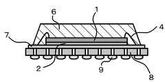
- FIG. 1 is a view showing a cross-sectional structure of an example of a semiconductor device using the resin composition for encapsulating a semiconductor according to the present invention.
- the semiconductor element 1 is fixed on the die pad 3 via the die bond material cured body 2.
- the electrode pad of the semiconductor element 1 and the lead frame 5 are connected by a gold wire 4.
- the semiconductor element 1 is sealed with a cured body 6 of a semiconductor sealing resin composition.
- FIG. 2 is a view showing a cross-sectional structure of an example of a single-sided sealing type semiconductor device using the semiconductor sealing resin composition according to the present invention.
- the semiconductor element 1 On the surface of the substrate 8, the semiconductor element 1 is fixed via the die-bonding material cured body 2 on the solder resist 7 of the laminated body in which the layer of the solder resist 7 is formed.
- the solder resist 7 on the electrode pad is removed by a developing method so that the electrode pad is exposed. Therefore, the semiconductor device of FIG. 2 is designed to connect the electrode pad of the semiconductor element 1 and the electrode pad on the substrate 8 by the gold wire 4.
- Phenol resin 1 1,6-naphthalenediol (Tokyo Chemical Industry Co., Ltd., melting point 136 ° C., molecular weight 160.2, purity 99.5%) 100 parts by mass, 4,4′-bischloromethylbiphenyl (Wako Pure Chemical) Kogyo Co., Ltd., purity 97.5%, molecular weight 251) 31.5 parts by mass and pure water 0.6 parts by mass were weighed into a separable flask, heated while purging with nitrogen, and stirred at the start of melting. Started. The system was allowed to react for 2 hours while maintaining the system temperature in the range of 150 ° C to 160 ° C.
- Phenol resin 3 1,6-naphthalenediol (manufactured by Tokyo Chemical Industry Co., Ltd., melting point 136 ° C., molecular weight 160.2, purity 99.5%) 100 parts by mass, 4,4′-bischloromethylbiphenyl (Wako Pure Chemical) Kogyo Co., Ltd., bischloromethylbiphenyl, purity 96%, molecular weight 251) 35.4 parts by mass and pure water 0.6 parts by mass are weighed into a separable flask and heated while replacing with nitrogen to start melting. At the same time, stirring was started. After reacting for 15 minutes while maintaining the system temperature in the range of 150 ° C.
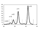
- a GPC chart is shown in FIG. 6, and an FD-MS chart is shown in FIG.
- Phenol resins 4 to 7 were used as phenol resins other than the phenol resin (A).
- Phenol resin 4 Naphthalenediol aralkyl resin having a phenylene skeleton represented by the following formula (15) (manufactured by Nippon Steel Chemical Co., Ltd., SN-375. Hydroxyl equivalent 99, softening point 70 ° C., ICI viscosity 0 at 150 ° C. .7 dPa ⁇ s).
- Phenol resin 5 Phenol aralkyl resin having a biphenylene skeleton (MEH-7851SS, manufactured by Meiwa Kasei Co., Ltd., hydroxyl group equivalent 203, softening point 67 ° C., ICI viscosity 0.7 dPa ⁇ s at 150 ° C.).
- Phenol resin 6 Triphenylmethane type phenol resin (Maywa Kasei Co., Ltd., MEH-7500, hydroxyl equivalent 97, softening point 110 ° C., ICI viscosity 5.8 dPa ⁇ s at 150 ° C.).
- Phenol resin 7 Phenol novolak resin (manufactured by Sumitomo Bakelite Co., Ltd., PR-HF-3, hydroxyl equivalent weight 104, softening point 80 ° C., ICI viscosity 5.8 dPa ⁇ s at 150 ° C.)
- the GPC measurement of the phenol resin 1 was performed under the following conditions. 6 ml of the solvent tetrahydrofuran (THF) was added to 20 mg of the phenol resin 1 sample and sufficiently dissolved, and subjected to GPC measurement.
- the GPC system includes WATERS module W2695, Tosoh Corporation TSK GUARDCOLUMN HHR-L (diameter 6.0 mm, tube length 40 mm, guard column), Tosoh Corporation TSK-GEL GMHHR-L (diameter 7. 8 mm, tube length 30 mm, two polystyrene gel columns), and a differential refractive index (RI) detector W2414 manufactured by WATERS, in series, were used.
- RI differential refractive index
- the flow rate of the pump was 0.5 ml / min, the temperature in the column and the differential refractometer was 40 ° C., and measurement was performed by injecting the measurement solution from a 100 ⁇ l injector.
- the FD-MS measurement of phenol resin 1 was performed under the following conditions. After adding 1 g of the solvent dimethyl sulfoxide to 10 mg of the phenol resin 1 sample and dissolving it sufficiently, it was applied to the FD emitter and subjected to measurement.
- an MS-FD15A manufactured by JEOL Ltd. is connected to the ionization section, and an MS-700 (model name: double focusing mass spectrometer) manufactured by JEOL Ltd. is connected to the detector. And used in the detection mass range (m / z) 50-2000.
- Epoxy resin 1 phenol aralkyl type epoxy resin having a biphenylene skeleton (manufactured by Nippon Kayaku Co., Ltd., NC3000, epoxy equivalent 276, softening point 58 ° C., ICI viscosity 1.11 dPa ⁇ s at 150 ° C.)
- Epoxy resin 2 phenol aralkyl type epoxy resin having a phenylene skeleton (manufactured by Nippon Kayaku Co., Ltd., NC2000, epoxy equivalent 238, softening point 52 ° C., ICI viscosity 1.2 dPa ⁇ s at 150 ° C.)
- Epoxy resin 3 Modified orthocresol novolak type epoxy resin (manufactured by DIC Corporation, HP-5000, epoxy equivalent 251, softening point 58 ° C., ICI viscosity 0.85 dPa ⁇ s at 150 ° C.)
- Epoxy resin 6 Bisphenol F type epoxy resin (manufactured by Toto Kasei Co., Ltd., YSLV-80XY, epoxy equivalent 190, softening point 80 ° C., ICI viscosity 0.03 dPa ⁇ s at 150 ° C.)
- Epoxy resin 7 bisphenol A type epoxy resin (manufactured by Japan Epoxy Resin Co., Ltd., YL6810, epoxy equivalent 172, softening point 45 ° C., softening point 107 ° C., ICI viscosity 0.03 dPa ⁇ s at 150 ° C.)
- Epoxy resin 8 biphenyl type epoxy resin (manufactured by Japan Epoxy Resin Co., Ltd., YX4000K, epoxy equivalent 185, softening point 107 ° C.
- Epoxy resin 9 Triphenylmethane type epoxy resin (manufactured by Japan Epoxy Resins Co., Ltd., 1032H-60, epoxy equivalent 171, softening point 60 ° C., ICI viscosity 1.3 dPa ⁇ s at 150 ° C.)
- the inorganic filler 100 parts by mass of fused spherical silica FB560 (average particle size 30 ⁇ m) manufactured by Denki Kagaku Kogyo Co., Ltd., synthetic spherical silica SO-C2 (average particle size 0.5 ⁇ m) 6.5 manufactured by Admatechs Co., Ltd. A blend of 7.5 parts by weight of synthetic spherical silica SO-C5 (average particle size 30 ⁇ m) manufactured by Admatechs Co., Ltd. was used.
- Compound (D1) Compound (D) represented by the following formula (16)
- Triphenylphosphine was used as another phosphorus compound.
- silane coupling agent 1 ⁇ -mercaptopropyltrimethoxysilane (manufactured by Shin-Etsu Chemical Co., Ltd., KBM-803)
- Silane coupling agent 2 ⁇ -glycidoxypropyltrimethoxysilane (manufactured by Shin-Etsu Chemical Co., Ltd., KBM-403)
- Silane coupling agent 3 N-phenyl-3-aminopropyltrimethoxysilane (manufactured by Shin-Etsu Chemical Co., Ltd., KBM-573)
- the following metal hydroxides 1 and 2 were used as metal hydroxides.
- Metal hydroxide-1 Magnesium hydroxide / zinc hydroxide solid solution composite metal hydroxide (Echo Mug Z-10, manufactured by Tateho Chemical Co., Ltd.).
- Metal hydroxide-2 Aluminum hydroxide (manufactured by Sumitomo Chemical Co., Ltd., CL-310).
- Phosphazene compound cyclophosphazene (manufactured by Otsuka Chemical Co., Ltd., SPE-100). Carbon black (MA600) manufactured by Mitsubishi Chemical Corporation was used as the colorant.
- As the release agent carnauba wax (Nikko carnauba, melting point 83 ° C.) manufactured by Nikko Fine Co., Ltd. was used.
- Example 1 The following components were mixed at room temperature with a mixer, melt-kneaded with a heating roll at 80 ° C. to 100 ° C., then cooled, and then pulverized to obtain a resin composition for semiconductor encapsulation.
- Phenolic resin 1 3.25 parts by weight Epoxy resin 1 9.25 parts by weight Inorganic filler 86.50 parts by weight
- Curing accelerator 1 (D1) 0.40 parts by weight Silane coupling agent 1 0.10 parts by weight Silane coupling agent 2 0.05 mass part Silane coupling agent 3 0.05 mass part Colorant 0.30 mass part Release agent 0.10 mass part
- the obtained resin composition for semiconductor sealing was evaluated about the following items. The evaluation results are shown in Table 1.
- the resin composition for semiconductor encapsulation obtained above was loaded into a tableting mold having a weight of 7.5 g and a size of ⁇ 16 mm using a rotary tableting machine, and tableted at a tableting pressure of 600 Pa. Got.
- the tablet was loaded into a tablet supply magazine and set inside the molding apparatus.
- Adhesion resistance The above-mentioned tablet was set in a magazine so that 15 tablets were stacked vertically, and left in a constant temperature bath at 25 ° C. and 30 ° C., and the fixed state of the tablet was confirmed after 8 hours.
- 1 is the contact surface that is fixed and cannot be separated by hand
- 0.5 is the contact surface that is fixed but can be easily separated
- 0 is the contact surface that is not fixed
- the total score is shown in the section of sticking resistance in Table 4.
- tablets are stacked vertically in a magazine in the automatic transfer unit of the molding machine vertically up to a height of 20 to 40 cm, and the surface temperature is about 20 to 30 ° C until molding.
- the tablet is fed and transported in the molding device by raising the push-up pin from the bottom of the magazine, so that the top tablet is pushed out from the top of the magazine and lifted by the mechanical arm to the transfer molding pot. Be transported. At this time, if the tablet sticks up and down during standby in the magazine, a conveyance failure occurs and productivity is impaired.
- Boiling water absorption rate disk-shaped test using a low-pressure transfer molding machine (KTS-30, manufactured by Kotaki Seiki Co., Ltd.) with a mold temperature of 175 ° C., an injection pressure of 9.8 MPa, a curing time of 120 s, a diameter of 50 mm, and a thickness of 3 mm Pieces were molded and heat treated at 175 ° C. for 4 hours. The weight change before the moisture absorption treatment of the test piece and after the boiling treatment in pure water for 24 hours was measured, and the water absorption rate of the test piece was shown as a percentage. The unit is%.
- the resin composition for semiconductor encapsulation obtained above showed a low water absorption of 0.27% or less (Reference Example 1).
- Solder resistance test 1 Using a low-pressure transfer molding machine (GP-ELF, manufactured by Daiichi Seiko Co., Ltd.) under conditions of a mold temperature of 180 ° C., an injection pressure of 7.4 MPa, and a curing time of 120 seconds. The resin composition is injected and a lead frame on which a semiconductor element (silicon chip) is mounted is sealed and molded, and 80 pQFP (Quad Flat Package, Cu lead frame, the size is 14 ⁇ 20 mm ⁇ thickness 2.00 mm, The semiconductor device is 7 ⁇ 7 mm ⁇ thickness 0.35 mm, and the semiconductor element and the inner lead portion of the lead frame are bonded with a gold wire with a diameter of 25 ⁇ m.
- GP-ELF low-pressure transfer molding machine
- Solder resistance test 2 Same as solder resistance test 1 except that six semiconductor devices heat-treated at 175 ° C. for 4 hours in the above-described solder resistance test 1 were treated at 85 ° C. and 60% relative humidity for 168 hours. The test was conducted. The semiconductor device produced using the resin composition for semiconductor encapsulation obtained above showed a good reliability of 0/6.
- High-temperature storage characteristics test Using a low-pressure transfer molding machine (GP-ELF, manufactured by Daiichi Seiko Co., Ltd.) under conditions of a mold temperature of 180 ° C., an injection pressure of 6.9 ⁇ 0.17 MPa, and 90 seconds.
- GP-ELF low-pressure transfer molding machine
- the resistance value of the semiconductor device was measured after the high temperature treatment, and the semiconductor device having 130% of the initial resistance value was regarded as defective. When the number of defective semiconductor devices was n, it was displayed as n / 10.
- the resin composition for semiconductor encapsulation obtained above showed a good reliability of 0/10.
- Examples 1 to 11 include a phenol resin (A), an epoxy resin (B), and an inorganic filler (C) having the structural units represented by the general formula (1) and the general formula (2).
- It is a resin composition, and includes those in which the proportion of the structural unit of the phenol resin (A) is changed, the type of the epoxy resin (B) is changed, the type of the compound (D) is changed, and the compound (E) is included. In either case, the results were excellent in the balance of fluidity (spiral flow), flame resistance, continuous moldability, solder resistance, and high-temperature storage characteristics.
- Comparative Example 1 using a naphthalenediol aralkyl resin having a phenylene skeleton as a curing agent is considered to absorb moisture due to a high hydroxyl group density, resulting in insufficient solder resistance results. Since the compatibility with the phenol aralkyl type epoxy resin was insufficient, the continuous moldability was insufficient. Since Comparative Example 2 using a phenol aralkyl resin having a biphenylene skeleton as a curing agent is low curable and highly oleophilic, the resin component tends to accumulate on the mold surface during continuous molding, resulting in continuous moldability. In addition, the glass transition temperature is low and the high-temperature storage characteristics are not sufficient.
- a resin composition for encapsulating a semiconductor which has good fluidity (spiral flow), flame resistance, solder resistance, and is excellent in continuous moldability and high-temperature storage characteristics. Suitable for stopping.
Landscapes
- Chemical & Material Sciences (AREA)
- Organic Chemistry (AREA)
- Health & Medical Sciences (AREA)
- Chemical Kinetics & Catalysis (AREA)
- Medicinal Chemistry (AREA)
- Polymers & Plastics (AREA)
- Epoxy Resins (AREA)
- Structures Or Materials For Encapsulating Or Coating Semiconductor Devices Or Solid State Devices (AREA)
- Polyoxymethylene Polymers And Polymers With Carbon-To-Carbon Bonds (AREA)
- Compositions Of Macromolecular Compounds (AREA)
Abstract
Description
たとえば、表面実装に用いられる半田については環境問題を背景とした無鉛半田への切り替えが進められている。無鉛半田の融点は従来の鉛/スズ半田に比べて高く、リフロー実装温度は従来の220~240℃から、240℃~260℃へと高くなり、半導体装置内の樹脂クラックや剥離が生じやすく、従来の封止用樹脂組成物では耐半田性が不足する場合がある。
また、従来の封止用樹脂組成物には難燃性を付与する目的から、難燃剤として臭素含有エポキシ樹脂と酸化アンチモンが使用されているが、近年の環境保護、安全性向上の観点からこれらの化合物を撤廃する機運が高まっている。
さらに近年では、自動車や携帯電話などの屋外での使用を前提とした電子機器が普及し、これらの用途では、従来のパソコンや家電製品よりも厳しい環境下での動作信頼性が求められる。特に車載用途においては、必須要求項目のひとつとして高温保管特性が求められ、150~180℃の高温下で半導体装置がその動作・機能を維持する必要が有る。
従来の技術としては、ナフタレン骨格を有するエポキシ樹脂、ナフタレン骨格を有するフェノール樹脂硬化剤とを組み合わせて、高温保管特性と耐半田性を高める手法(特許文献1,2)や、リン酸含有化合物を配合することによって、高温保管特性と耐燃性を高める手法(特許文献3,4)が提案されているものの、これらは耐燃性、連続成形性、耐半田性のバランスが十分とは言い難い場合が有る。以上のように、車載用電子機器の小型化と普及にあたっては、耐燃性・耐半田性・高温保管特性・連続成形性をバランスよく満たす封止用樹脂組成物が求められる。
[1]下記一般式(1)で表される成分を含むフェノール樹脂(A)と、
エポキシ樹脂(B)と、
無機充填剤(C)と、を含むことを特徴とする半導体封止用樹脂組成物。


[4]前記フェノール樹脂(A)は、前記一般式(1)におけるn=0の成分を、全フェノール樹脂(A)中に、25質量%以上70質量%以下含むものである[1]ないし[3]のいずれか1項に半導体封止用樹脂組成物。
[5]前記フェノール樹脂(A)は、ゲルパーミエーションクロマトグラフィー(GPC)測定方法における面積換算法において、R1が前記一般式(2)で表される基である成分を、全フェノール樹脂(A)中に、20面積%以上80面積%以下含有するものである[2]ないし[4]のいずれか1項に記載の半導体封止用樹脂組成物。
[6][1]ないし[5]のいずれか1項に記載の半導体封止用樹脂組成物を用い、半導体素子を封止してなる半導体装置。

従来、高温保管特性と耐燃性とを高める手法は、たとえば、ナフタレン骨格を有するエポキシ樹脂とナフタレン骨格を有するフェノール樹脂硬化剤との組み合わせ、あるいは、リン酸含有化合物の配合(特許文献3,4)を挙げることができるが、これらの樹脂組成物は硬化性が低下し、連続成型性が低下する場合があった。
これに対し、本発明のフェノール樹脂(A)を用いた半導体封止用樹脂組成物は、流動性と耐固着性とのバランスに優れる。

なお、GPC測定により得られるチャートの各ピークの構造は、各フラクションに分離した後にNMR分析、もしくはFD-MSによる分析により確認することができる。




これらの中でも、入手容易性という観点からは4,4’-ビスメトキシメチルビフェニルが好ましく、重合触媒を削減でき、不純物を減らすことができる点で4,4’-ビスクロロメチルビフェニルが好ましい。
これらの中でも、得られるフェノール樹脂の軟化点が比較的低くエポキシ樹脂との溶融混練が容易であるという点で、1,6-ジヒドロキシナフタレンが好ましい。
これらの中でも、酸性触媒を併用しなくてもよいという点では、ベンジルクロライド、ベンジルブロマイドが好ましい。
併用できる硬化剤としては、特に限定されないが、例えば重付加型の硬化剤、触媒型の硬化剤、縮合型の硬化剤などを挙げることができる。
硬化剤全体の配合割合の下限値については、特に限定されないが、全半導体封止用樹脂組成物中に、0.8質量%以上であることが好ましく1.5質量%以上であることがより好ましい。配合割合の下限値が上記範囲内であると、充分な流動性を得ることができる。また、硬化剤全体の配合割合の上限値についても、特に限定されないが、全半導体封止用樹脂組成物中に、10質量%以下であることが好ましく、8質量%以下であることがより好ましい。配合割合の上限値が上記範囲内であると、良好な耐半田性を得ることができる。
なお、フェノール樹脂とエポキシ樹脂とは、全エポキシ樹脂のエポキシ基数(EP)と、全フェノール樹脂のフェノール性水酸基数(OH)との当量比(EP)/(OH)が、0.8以上、1.3以下となるように配合することが好ましい。当量比が上記範囲内であると、得られる樹脂組成物を成形する際、十分な硬化特性を得ることができる。
なお、後述する、水酸化アルミニウム、水酸化マグネシウムなどの金属水酸化物や、硼酸亜鉛、モリブデン酸亜鉛、三酸化アンチモンなどの無機系難燃剤を用いる場合には、これらの無機系難燃剤と上記無機充填剤の合計量を上記範囲内とすることが望ましい。


またホスフィン化合物とキノン化合物との付加物に用いるキノン化合物としては、o-ベンゾキノン、p-ベンゾキノン、アントラキノン類が挙げられ、中でもp-ベンゾキノンが保存安定性の点から好ましい。
ホスフィン化合物とキノン化合物との付加物の製造方法としては、有機第三ホスフィンとベンゾキノン類の両者が溶解することができる溶媒中で接触、混合させることにより付加物を得ることができる。溶媒としてはアセトンやメチルエチルケトンなどのケトン類で付加物への溶解性が低いものがよい。しかしこれに限定されるものではない。
一般式(9)で表される化合物において、リン原子に結合するR9、R10およびR11がフェニル基であり、かつR12、R13およびR14が水素原子である化合物、すなわち1,4-ベンゾキノンとトリフェニルホスフィンを付加させた化合物が半導体封止用樹脂組成物の硬化物の熱時弾性率を低く維持できる点で好ましい。

また、一般式(10)中のZ1は、芳香環または複素環を有する有機基、あるいは脂肪族基を表し、これらの具体的な例としては、メチル基、エチル基、プロピル基、ブチル基、ヘキシル基およびオクチル基などの脂肪族炭化水素基や、フェニル基、ベンジル基、ナフチル基およびビフェニル基などの芳香族炭化水素基、グリシジルオキシプロピル基、メルカプトプロピル基、アミノプロピル基およびビニル基などの反応性置換基などが挙げられるが、これらの中でも、メチル基、エチル基、フェニル基、ナフチル基およびビフェニル基が一般式(10)の熱安定性が向上するという点で、より好ましい。
また、化合物(E)は、半導体封止用樹脂組成物の溶融粘度を下げ、流動性を向上させる効果も有するものである。化合物(E)としては、下記一般式(11)で表される単環式化合物または下記一般式(12)で表される多環式化合物などを用いることができ、これらの化合物は水酸基以外の置換基を有していてもよい。


尚、化合物(E)の一部は、前記一般式(1)で表されるフェノール樹脂(A)に該当する場合がある。
この場合は、化合物(E)のうち、フェノール樹脂(A)に該当する化合物(E)は、フェノール樹脂(A)に含め、フェノール樹脂(A)の配合量とする。
その例としては特に限定されないが、エポキシシラン、アミノシラン、ウレイドシラン、メルカプトシランなどが挙げられ、エポキシ樹脂と無機充填剤との間で反応し、エポキシ樹脂と無機充填剤の界面強度を向上させるものであればよい。また、シランカップリング剤は、前述の化合物(E)と併用することで、樹脂組成物の溶融粘度を下げ、流動性を向上させるという化合物(E)の効果を高めることもできるものである。
エポキシシランとしては、例えば、γ-グリシドキシプロピルトリエトキシシラン、γ-グリシドキシプロピルトリメトキシシラン、γ-グリシドキシプロピルメチルジメトキシシラン、β-(3,4エポキシシクロヘキシル)エチルトリメトキシシランなどが挙げられる。
また、アミノシランとしては、例えば、γ-アミノプロピルトリエトキシシラン、γ-アミノプロピルトリメトキシシラン、N-β(アミノエチル)γ-アミノプロピルトリメトキシシラン、N-β(アミノエチル)γ-アミノプロピルメチルジメトキシシラン、N-フェニルγ-アミノプロピルトリエトキシシラン、N-フェニルγ-アミノプロピルトリメトキシシラン、N-β(アミノエチル)γ-アミノプロピルトリエトキシシラン、N-6-(アミノヘキシル)3-アミノプロピルトリメトキシシラン、N-(3-(トリメトキシシリルプロピル)-1,3-ベンゼンジメタナンなどが挙げられる。また、ウレイドシランとしては、例えば、γ-ウレイドプロピルトリエトキシシラン、ヘキサメチルジシラザンなどが挙げられる。
また、メルカプトシランとしては、例えば、γ-メルカプトプロピルトリメトキシシランなどが挙げられる。これらのシランカップリング剤は1種類を単独で用いても2種類以上を併用してもよい。
本発明の半導体封止用樹脂組成物を用いて半導体装置を製造する方法としては、例えば、半導体素子を搭載したリードフレームまたは回路基板などを金型キャビティ内に設置した後、半導体封止用樹脂組成物をトランスファーモールド、コンプレッションモールド、インジェクションモールドなどの成形方法で成形、硬化させることにより、この半導体素子を封止する方法が挙げられる。
封止される半導体素子としては、例えば、集積回路、大規模集積回路、トランジスタ、サイリスタ、ダイオード、固体撮像素子などが挙げられるが、これらに限定されない。
得られる半導体装置の形態としては、例えば、デュアル・インライン・パッケージ(DIP)、プラスチック・リード付きチップ・キャリヤ(PLCC)、クワッド・フラット・パッケージ(QFP)、ロー・プロファイル・クワッド・フラット・パッケージ(LQFP)、スモール・アウトライン・パッケージ(SOP)、スモール・アウトライン・Jリード・パッケージ(SOJ)、薄型スモール・アウトライン・パッケージ(TSOP)、薄型クワッド・フラット・パッケージ(TQFP)、テープ・キャリア・パッケージ(TCP)、ボール・グリッド・アレイ(BGA)、チップ・サイズ・パッケージ(CSP)などが挙げられるが、これらに限定されない。
半導体封止用樹脂組成物のトランスファーモールドなどの成形方法により半導体素子が封止された半導体装置は、そのまま、あるいは80℃から200℃程度の温度で、10分から10時間程度の時間をかけてこの樹脂組成物を完全硬化させた後、電子機器などに搭載される。
図1は、本発明に係る半導体封止用樹脂組成物を用いた半導体装置の一例について、断面構造を示した図である。ダイパッド3上に、ダイボンド材硬化体2を介して半導体素子1が固定されている。半導体素子1の電極パッドとリードフレーム5との間は金線4によって接続されている。半導体素子1は、半導体封止用樹脂組成物の硬化体6によって封止されている。
図2は、本発明に係る半導体封止用樹脂組成物を用いた片面封止型の半導体装置の一例について、断面構造を示した図である。基板8の表面に、ソルダーレジスト7の層が形成された積層体のソルダーレジスト7上にダイボンド材硬化体2を介して半導体素子1を固定する。
尚、半導体素子1と基板8との導通をとるため、電極パッドが露出するよう、電極パッド上のソルダーレジスト7は、現像法により除去されている。
従って、図2の半導体装置は、半導体素子1の電極パッドと基板8上の電極パッドとの間は金線4によって接続する設計となっている。
半導体装置に封止用樹脂組成物を封止し、硬化体6を形成することによって、基板8の半導体素子1が搭載された片面側のみが封止された半導体装置を得ることができる。基板8上の電極パッドは基板8上の非封止面側の半田ボール9と内部で接合されている。
フェノール樹脂1:1,6―ナフタレンジオール(東京化成工業株式会社製、融点136℃、分子量160.2、純度99.5%)100質量部、4,4’-ビスクロロメチルビフェニル(和光純薬工業(株)製、純度97.5%、分子量251)31.5質量部、純水0.6質量部をセパラブルフラスコに秤量し、窒素置換しながら加熱し、溶融の開始に併せて攪拌を開始した。系内温度を150℃から160℃の範囲に維持しながら2時間反応させた。上記の反応の間、反応によって系内に発生する塩酸は、窒素気流によって系外へ排出した。反応終了後、150℃、2mmHgの減圧条件で残留する塩酸と水分を留去し、下記式(13)で表されるフェノール樹脂1(水酸基当量102、軟化点75℃、150℃におけるICI粘度1.15dPa・s、GPCの面積法より算出したn=0の含有割合51%、n=0~2の含有割合95%、nの平均値0.72)を得た。GPCチャートを図3に、FD-MSチャートを図4に示す。
フェノール樹脂2:フェノール樹脂1の合成において、1,6―ナフタレンジオールを115質量部としてフェノール樹脂1と同様の操作を行い、下記式(13)で表されるフェノール樹脂2(水酸基当量98、軟化点84℃、150℃におけるICI粘度0.9dPa・s。GPCの面積法より算出したn=0の含有割合55%、n=0~2の含有割合95%、nの平均値0.65)を得た。GPCチャートを図5に示す。
フェノール樹脂3:1,6―ナフタレンジオール(東京化成工業株式会社製、融点136℃、分子量160.2、純度99.5%)100質量部、4,4’-ビスクロロメチルビフェニル(和光純薬工業(株)製、ビスクロロメチルビフェニル、純度96%、分子量251)35.4質量部、純水0.6質量部をセパラブルフラスコに秤量し、窒素置換しながら加熱し、溶融の開始に併せて攪拌を開始した。系内温度を150℃から160℃の範囲に維持しながら15分間反応させたのち、反応系内にベンジルクロライド(関東化学(株)製特級試薬、沸点179℃、分子量126.6、純度99.5%)40質量部、純水0.6質量部を滴下し、さらに2時間反応させた。上記の反応の間、反応によって系内に発生する塩酸は、窒素気流によって系外へ排出した。反応終了後、150℃、2mmHgの減圧条件で残留する塩酸と水分を留去し、下記式(14)で表される構造で、h1~h4の和は最大で3であるフェノール樹脂3(水酸基当量129、軟化点67℃、150℃におけるICI粘度1.8dPa・s、GPCの面積法より算出したn=0の含有割合52%、n=0~2の含有割合93%、nの平均値0.70、フェノール樹脂3中のベンジル基を有する成分の含有割合は、GPCの面積法で50面積%)を得た。GPCチャートを図6に、FD-MSチャートを図7に示す。


フェノール樹脂4:下記式(15)で表されるフェニレン骨格を有するナフタレンジオールアラルキル樹脂(新日鐵化学(株)製、SN-375。水酸基当量99、軟化点70℃、150℃におけるICI粘度0.7dPa・s)。
フェノール樹脂5:ビフェニレン骨格を有するフェノールアラルキル樹脂(明和化成(株)製、MEH-7851SS。水酸基当量203、軟化点67℃、150℃におけるICI粘度0.7dPa・s)。
フェノール樹脂6:トリフェニルメタン型フェノール樹脂(明和化成(株)製、MEH-7500。水酸基当量97、軟化点110℃、150℃におけるICI粘度5.8dPa・s)。
フェノール樹脂7:フェノールノボラック樹脂(住友ベークライト(株)製、PR-HF-3。水酸基当量104、軟化点80℃、150℃におけるICI粘度5.8dPa・s)
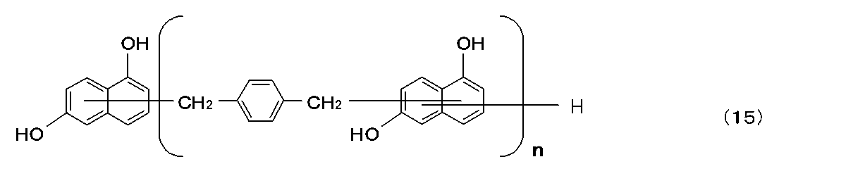
フェノール樹脂1のFD-MS測定は次の条件で行った。フェノール樹脂1の試料10mgに溶剤ジメチルスルホキシド1gを加えて十分溶解したのち、FDエミッターに塗布の後、測定に供した。FD-MSシステムは、イオン化部に日本電子(株)製のMS-FD15Aを、検出器に日本電子(株)製のMS-700(機種名:二重収束型質量分析装置)とを接続して用い、検出質量範囲(m/z)50~2000にて測定した。
エポキシ樹脂1:ビフェニレン骨格を有するフェノールアラルキル型エポキシ樹脂(日本化薬(株)製、NC3000。エポキシ当量276、軟化点58℃、150℃におけるICI粘度1.11dPa・s)
エポキシ樹脂2:フェニレン骨格を有するフェノールアラルキル型エポキシ樹脂(日本化薬(株)製、NC2000。エポキシ当量238、軟化点52℃、150℃におけるICI粘度1.2dPa・s)
エポキシ樹脂3:変性オルソクレゾールノボラック型エポキシ樹脂(DIC(株)製、HP-5000。エポキシ当量251、軟化点58℃、150℃におけるICI粘度0.85dPa・s。
エポキシ樹脂4:ジシクロペンタジエン型エポキシ樹脂(DIC(株)製、HP-7200L、エポキシ当量244、軟化点56℃、150℃におけるICI粘度0.24dPa・s。)
エポキシ樹脂5:オルソクレゾールノボラック型エポキシ樹脂(DIC(株)製、N660。エポキシ当量210、軟化点62℃、150℃におけるICI粘度2.34dPa・s。
エポキシ樹脂6:ビスフェノールF型エポキシ樹脂(東都化成(株)製、YSLV-80XY、エポキシ当量190、軟化点80℃、150℃におけるICI粘度0.03dPa・s。)
エポキシ樹脂7:ビスフェノールA型エポキシ樹脂(ジャパンエポキシレジン(株)製、YL6810、エポキシ当量172、軟化点45℃、軟化点107℃、150℃におけるICI粘度0.03dPa・s)
エポキシ樹脂8:ビフェニル型エポキシ樹脂(ジャパンエポキシレジン(株)製、YX4000K、エポキシ当量185、軟化点107℃、150℃におけるICI粘度0.1dPa・s)
エポキシ樹脂9:トリフェニルメタン型エポキシ樹脂(ジャパンエポキシレジン(株)製、1032H-60、エポキシ当量171、軟化点60℃、150℃におけるICI粘度1.3dPa・s)
無機充填剤としては、電気化学工業(株)製溶融球状シリカFB560(平均粒径30μm)100質量部、(株)アドマテックス製合成球状シリカSO-C2(平均粒径0.5μm)6.5質量部、(株)アドマテックス製合成球状シリカSO-C5(平均粒径30μm)7.5質量部のブレンドを使用した。
化合物(D1):下記式(16)で表される化合物(D)

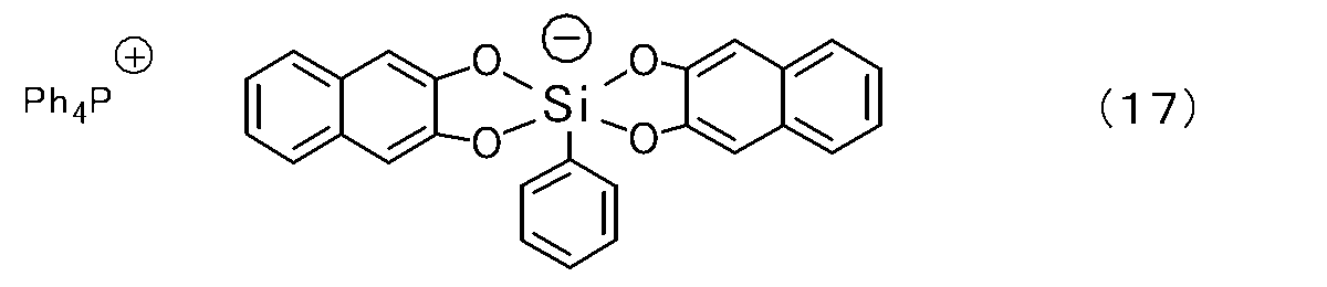
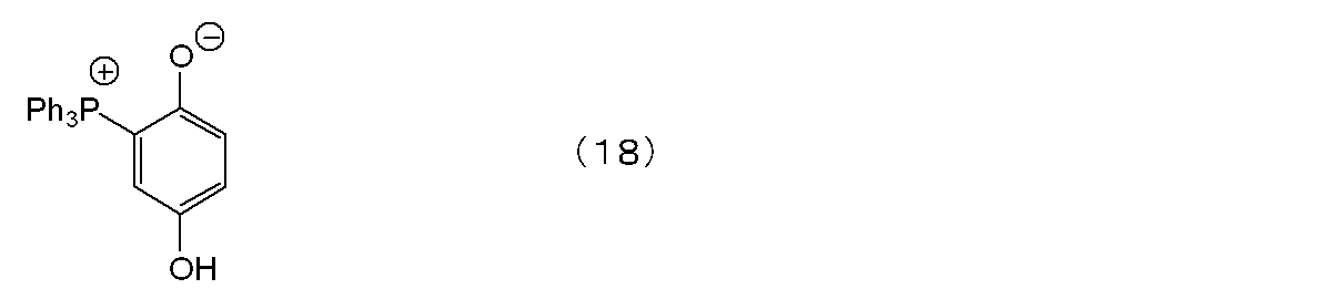


シランカップリング剤1:γ-メルカプトプロピルトリメトキシシラン(信越化学工業(株)製、KBM-803)
シランカップリング剤2:γ-グリシドキシプロピルトリメトキシシラン(信越化学工業(株)製、KBM-403)
シランカップリング剤3:N-フェニル-3-アミノプロピルトリメトキシシラン(信越化学工業(株)製、KBM-573)
金属水酸化物は、以下の金属水酸化物1および2を使用した。
金属水酸化物-1:水酸化マグネシウム・水酸化亜鉛固溶体複合金属水酸化物(タテホ化学工業(株)製、エコーマグZ-10)。
金属水酸化物-2:水酸化アルミニウム(住友化学(株)製、CL-310)。
ホスファゼン化合物:シクロホスファゼン(大塚化学(株)製、SPE-100)。
着色剤は、三菱化学(株)製のカーボンブラック(MA600)を使用した。
離型剤は、日興ファイン(株)製のカルナバワックス(ニッコウカルナバ、融点83℃)を使用した。
以下の成分をミキサーにて常温で混合し、80℃~100℃の加熱ロールで溶融混練し、その後冷却し、次いで粉砕して、半導体封止用樹脂組成物を得た。
フェノール樹脂1 3.25質量部
エポキシ樹脂1 9.25質量部
無機充填剤 86.50質量部
硬化促進剤1(D1) 0.40質量部
シランカップリング剤1 0.10質量部
シランカップリング剤2 0.05質量部
シランカップリング剤3 0.05質量部
着色剤 0.30質量部
離型剤 0.10質量部
得られた半導体封止用樹脂組成物を、以下の項目について評価した。評価結果を表1に示す。
表1ないし表3の配合に従い、実施例1と同様にして半導体封止用樹脂組成物を製造し、実施例1と同様にして評価した。評価結果を表1ないし3に示す。


一方、フェニレン骨格を有するナフタレンジオールアラルキル樹脂を硬化剤に用いた比較例1は、水酸基密度が高いために吸湿しやいと考えられ、結果として耐半田性結果が十分でないこと、さらに、ビフェニレン骨格を有するフェノールアラルキル型エポキシ樹脂との相溶性が十分でないために連続成型性が不十分な結果となった。ビフェニレン骨格を有するフェノールアラルキル樹脂を硬化剤に用いた比較例2は、低硬化性かつ高親油性であるために、連続成型時に金型表面に樹脂成分が蓄積しやすく、結果として連続成型性が十分でなく、さらにガラス転移点温度が低いために高温保管特性も十分ではない。トリフェニルメタン型フェノール樹脂を硬化剤に用いた比較例3は、架橋密度が高いために燃焼時に樹脂表面にクラックが生じて耐燃性が十分でなく、また水酸基密度と架橋密度が高いために、吸水性が高く、かつ半田リフロー温度における熱応力も高いために耐半田性が十分でない。
参考例1、および2から明らかなように実施例1、及び2の樹脂組成物を用いたものは前記特性の優れたバランスに加え、耐固着性にも優れる結果となった。
一方、参考例3に示す実施例3に用いた樹脂組成物は、低吸水性に優れることから更なる過酷な条件における耐半田性にも優れることが期待できる。
従って、より高い信頼性が要求される半導体封止材料に好適に適用できると推察する。
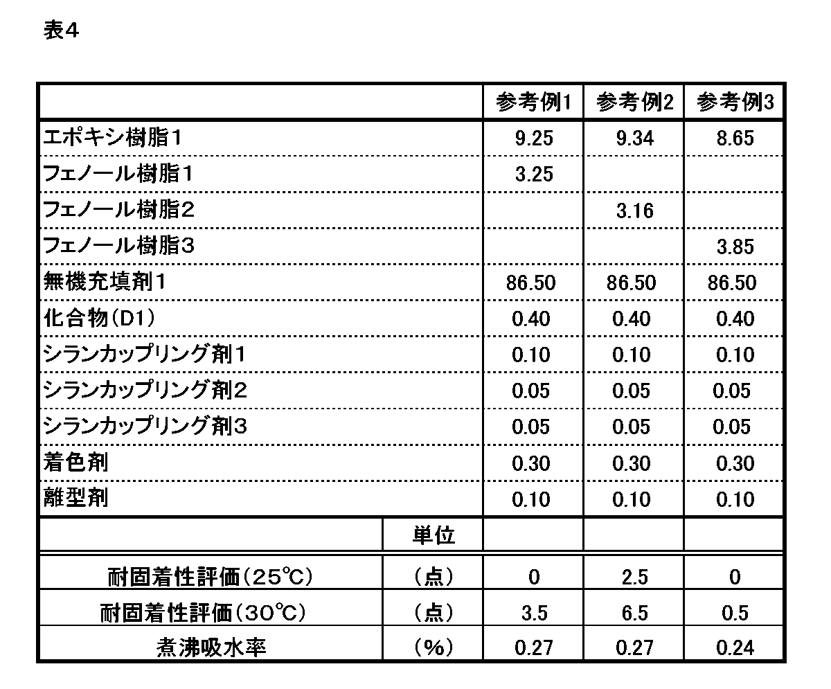
この出願は、平成21年6月22日に出願された日本特許出願特願2009-148048を基礎とする優先権を主張し、その開示の全てをここに取り込む。
Claims (6)
- 下記一般式(1)で表される成分を含むフェノール樹脂(A)と、
エポキシ樹脂(B)と、
無機充填剤(C)と、を含むことを特徴とする半導体封止用樹脂組成物。

- 前記フェノール樹脂(A)は、前記一般式(1)におけるR1が下記一般式(2)で表される基である成分を含む、請求項1に記載の半導体封止用樹脂組成物。

- 前記フェノール樹脂(A)は、n=0~2の成分を、全フェノール樹脂(A)中に、50質量%以上100質量%以下含有するものである請求項1または2に記載の半導体封止用樹脂組成物。
- 前記フェノール樹脂(A)は、n=0の成分を、全フェノール樹脂(A)中に、25質量%以上70質量%以下含むものである請求項1ないし3のいずれか1項に記載の半導体封止用樹脂組成物。
- 前記フェノール樹脂(A)は、ゲルパーミエーションクロマトグラフィー(GPC)測定方法における面積換算法において、R1が前記一般式(2)で表される基である成分を、全フェノール樹脂(A)中に、20面積%以上80面積%以下含有するものである請求項2ないし4のいずれか1項に記載の半導体封止用樹脂組成物。
- 請求項1ないし5のいずれか1項に記載の半導体封止用樹脂組成物を用い、半導体素子を封止してなる半導体装置。
Priority Applications (4)
| Application Number | Priority Date | Filing Date | Title |
|---|---|---|---|
| CN201080027933.XA CN102459397B (zh) | 2009-06-22 | 2010-06-16 | 半导体密封用树脂组合物、以及半导体装置 |
| SG2011092178A SG176825A1 (en) | 2009-06-22 | 2010-06-16 | Resin composition for encapsulating semiconductor and semiconductor device |
| JP2011519559A JP5692070B2 (ja) | 2009-06-22 | 2010-06-16 | 半導体封止用樹脂組成物、及び半導体装置 |
| US13/376,553 US8502399B2 (en) | 2009-06-22 | 2010-06-16 | Resin composition for encapsulating semiconductor and semiconductor device |
Applications Claiming Priority (2)
| Application Number | Priority Date | Filing Date | Title |
|---|---|---|---|
| JP2009-148048 | 2009-06-22 | ||
| JP2009148048 | 2009-06-22 |
Publications (1)
| Publication Number | Publication Date |
|---|---|
| WO2010150487A1 true WO2010150487A1 (ja) | 2010-12-29 |
Family
ID=43386275
Family Applications (1)
| Application Number | Title | Priority Date | Filing Date |
|---|---|---|---|
| PCT/JP2010/003990 Ceased WO2010150487A1 (ja) | 2009-06-22 | 2010-06-16 | 半導体封止用樹脂組成物、及び半導体装置 |
Country Status (8)
| Country | Link |
|---|---|
| US (1) | US8502399B2 (ja) |
| JP (1) | JP5692070B2 (ja) |
| KR (1) | KR20120040183A (ja) |
| CN (1) | CN102459397B (ja) |
| MY (1) | MY155689A (ja) |
| SG (1) | SG176825A1 (ja) |
| TW (1) | TWI477551B (ja) |
| WO (1) | WO2010150487A1 (ja) |
Cited By (6)
| Publication number | Priority date | Publication date | Assignee | Title |
|---|---|---|---|---|
| WO2013047696A1 (ja) * | 2011-09-29 | 2013-04-04 | 日立化成株式会社 | エポキシ樹脂組成物及び電子部品装置 |
| CN103975506A (zh) * | 2011-11-29 | 2014-08-06 | 住友电木株式会社 | 固定用树脂组合物、转子、汽车和转子的制造方法 |
| JP2020063392A (ja) * | 2018-10-18 | 2020-04-23 | 味の素株式会社 | 樹脂組成物 |
| WO2020129248A1 (ja) * | 2018-12-21 | 2020-06-25 | 日立化成株式会社 | 封止用樹脂組成物及び電子部品装置 |
| JP2021195480A (ja) * | 2020-06-16 | 2021-12-27 | 昭和電工マテリアルズ株式会社 | 封止用樹脂組成物及び電子部品装置 |
| WO2022118749A1 (ja) * | 2020-12-03 | 2022-06-09 | 住友ベークライト株式会社 | 封止用樹脂組成物および半導体装置 |
Families Citing this family (9)
| Publication number | Priority date | Publication date | Assignee | Title |
|---|---|---|---|---|
| US20120205822A1 (en) * | 2009-10-26 | 2012-08-16 | Yusuke Tanaka | Resin composition for encapsulating semiconductor and semiconductor device using the resin composition |
| CN102633990A (zh) * | 2012-04-05 | 2012-08-15 | 广东生益科技股份有限公司 | 环氧树脂组合物及使用其制作的半固化片与覆铜箔层压板 |
| CN104798194B (zh) * | 2013-01-11 | 2017-07-18 | 三菱电机株式会社 | 半导体器件 |
| JP5793160B2 (ja) * | 2013-03-28 | 2015-10-14 | 日東電工株式会社 | 電子デバイス封止用樹脂シート及び電子デバイスパッケージの製造方法 |
| KR102264524B1 (ko) * | 2015-03-23 | 2021-06-15 | 스미토모 베이클리트 컴퍼니 리미티드 | 봉지용 수지 조성물, 반도체 장치 및 반도체 장치의 제조 방법 |
| JP6980986B2 (ja) * | 2016-04-22 | 2021-12-15 | 住友ベークライト株式会社 | 半導体封止用樹脂組成物および半導体装置 |
| JP6989044B1 (ja) * | 2021-03-31 | 2022-01-05 | 住友ベークライト株式会社 | 封止構造体の製造方法およびタブレット |
| CN116478648B (zh) * | 2022-11-17 | 2025-12-30 | 江苏中科科化新材料股份有限公司 | 一种环氧塑封料及其制备方法与应用 |
| CN115981099A (zh) * | 2022-12-29 | 2023-04-18 | Tcl华星光电技术有限公司 | 光刻胶组合物及光刻胶图案化的方法 |
Citations (4)
| Publication number | Priority date | Publication date | Assignee | Title |
|---|---|---|---|---|
| JPH11255688A (ja) * | 1998-03-10 | 1999-09-21 | Nippon Steel Chem Co Ltd | 新規多価ヒドロキシ化合物、新規エポキシ樹脂、それらの製造方法、それらを用いたエポキシ樹脂組成物及びその硬化物 |
| JP2004059792A (ja) * | 2002-07-30 | 2004-02-26 | Nippon Steel Chem Co Ltd | 多価ヒドロキシ樹脂、エポキシ樹脂、それらの製造法、それらを用いたエポキシ樹脂組成物及び硬化物 |
| JP2004123859A (ja) * | 2002-10-01 | 2004-04-22 | Nippon Steel Chem Co Ltd | 多価ヒドロキシ樹脂、エポキシ樹脂、それらの製造法、それらを用いたエポキシ樹脂組成物及び硬化物 |
| WO2007007827A1 (ja) * | 2005-07-13 | 2007-01-18 | Ube Industries, Ltd. | ビフェニレン架橋フェノールノボラック樹脂ならびにその用途 |
Family Cites Families (6)
| Publication number | Priority date | Publication date | Assignee | Title |
|---|---|---|---|---|
| JPH06216280A (ja) | 1993-01-21 | 1994-08-05 | Mitsubishi Electric Corp | 半導体封止用エポキシ樹脂組成物およびそれを用いた半導体装置 |
| US6830825B2 (en) | 2001-04-23 | 2004-12-14 | Sumitomo Bakelite Company, Ltd. | Epoxy resin composition and semiconductor device |
| JP2003292731A (ja) | 2002-03-29 | 2003-10-15 | Sumitomo Bakelite Co Ltd | エポキシ樹脂組成物及び半導体装置 |
| JP2004043613A (ja) | 2002-07-11 | 2004-02-12 | Sumitomo Bakelite Co Ltd | エポキシ樹脂組成物及び半導体装置 |
| JP4844733B2 (ja) | 2005-06-24 | 2011-12-28 | 信越化学工業株式会社 | 半導体封止用エポキシ樹脂組成物及び半導体装置 |
| KR101195408B1 (ko) * | 2006-09-13 | 2012-10-29 | 스미토모 베이클라이트 가부시키가이샤 | 반도체 장치 |
-
2010
- 2010-06-16 SG SG2011092178A patent/SG176825A1/en unknown
- 2010-06-16 JP JP2011519559A patent/JP5692070B2/ja not_active Expired - Fee Related
- 2010-06-16 WO PCT/JP2010/003990 patent/WO2010150487A1/ja not_active Ceased
- 2010-06-16 US US13/376,553 patent/US8502399B2/en not_active Expired - Fee Related
- 2010-06-16 CN CN201080027933.XA patent/CN102459397B/zh not_active Expired - Fee Related
- 2010-06-16 MY MYPI2011005871A patent/MY155689A/en unknown
- 2010-06-16 KR KR1020127000321A patent/KR20120040183A/ko not_active Ceased
- 2010-06-22 TW TW099120222A patent/TWI477551B/zh not_active IP Right Cessation
Patent Citations (4)
| Publication number | Priority date | Publication date | Assignee | Title |
|---|---|---|---|---|
| JPH11255688A (ja) * | 1998-03-10 | 1999-09-21 | Nippon Steel Chem Co Ltd | 新規多価ヒドロキシ化合物、新規エポキシ樹脂、それらの製造方法、それらを用いたエポキシ樹脂組成物及びその硬化物 |
| JP2004059792A (ja) * | 2002-07-30 | 2004-02-26 | Nippon Steel Chem Co Ltd | 多価ヒドロキシ樹脂、エポキシ樹脂、それらの製造法、それらを用いたエポキシ樹脂組成物及び硬化物 |
| JP2004123859A (ja) * | 2002-10-01 | 2004-04-22 | Nippon Steel Chem Co Ltd | 多価ヒドロキシ樹脂、エポキシ樹脂、それらの製造法、それらを用いたエポキシ樹脂組成物及び硬化物 |
| WO2007007827A1 (ja) * | 2005-07-13 | 2007-01-18 | Ube Industries, Ltd. | ビフェニレン架橋フェノールノボラック樹脂ならびにその用途 |
Cited By (15)
| Publication number | Priority date | Publication date | Assignee | Title |
|---|---|---|---|---|
| US10865332B2 (en) | 2011-09-29 | 2020-12-15 | Showa Denko Materials Co., Ltd. | Epoxy resin composition and electronic component device |
| JPWO2013047696A1 (ja) * | 2011-09-29 | 2015-03-26 | 日立化成株式会社 | エポキシ樹脂組成物及び電子部品装置 |
| EP2762511A4 (en) * | 2011-09-29 | 2015-07-29 | Hitachi Chemical Co Ltd | Epoxy resin composition and electronic component device |
| WO2013047696A1 (ja) * | 2011-09-29 | 2013-04-04 | 日立化成株式会社 | エポキシ樹脂組成物及び電子部品装置 |
| US11767449B2 (en) | 2011-09-29 | 2023-09-26 | Resonac Corporation | Epoxy resin composition and electronic component device |
| CN103975506A (zh) * | 2011-11-29 | 2014-08-06 | 住友电木株式会社 | 固定用树脂组合物、转子、汽车和转子的制造方法 |
| US9997968B2 (en) | 2011-11-29 | 2018-06-12 | Sumitomo Bakelite Co., Ltd. | Fixing resin composition, rotor, automobile, and method of manufacturing rotor |
| CN110752687A (zh) * | 2011-11-29 | 2020-02-04 | 住友电木株式会社 | 固定用树脂组合物、转子、汽车和转子的制造方法 |
| JP2020063392A (ja) * | 2018-10-18 | 2020-04-23 | 味の素株式会社 | 樹脂組成物 |
| JP7230421B2 (ja) | 2018-10-18 | 2023-03-01 | 味の素株式会社 | 樹脂組成物 |
| JPWO2020129248A1 (ja) * | 2018-12-21 | 2021-12-02 | 昭和電工マテリアルズ株式会社 | 封止用樹脂組成物及び電子部品装置 |
| WO2020129248A1 (ja) * | 2018-12-21 | 2020-06-25 | 日立化成株式会社 | 封止用樹脂組成物及び電子部品装置 |
| JP2021195480A (ja) * | 2020-06-16 | 2021-12-27 | 昭和電工マテリアルズ株式会社 | 封止用樹脂組成物及び電子部品装置 |
| WO2022118749A1 (ja) * | 2020-12-03 | 2022-06-09 | 住友ベークライト株式会社 | 封止用樹脂組成物および半導体装置 |
| JPWO2022118749A1 (ja) * | 2020-12-03 | 2022-06-09 |
Also Published As
| Publication number | Publication date |
|---|---|
| TW201120128A (en) | 2011-06-16 |
| KR20120040183A (ko) | 2012-04-26 |
| JP5692070B2 (ja) | 2015-04-01 |
| SG176825A1 (en) | 2012-01-30 |
| CN102459397A (zh) | 2012-05-16 |
| CN102459397B (zh) | 2014-05-07 |
| JPWO2010150487A1 (ja) | 2012-12-06 |
| TWI477551B (zh) | 2015-03-21 |
| US8502399B2 (en) | 2013-08-06 |
| US20120080809A1 (en) | 2012-04-05 |
| MY155689A (en) | 2015-11-13 |
Similar Documents
| Publication | Publication Date | Title |
|---|---|---|
| JP5692070B2 (ja) | 半導体封止用樹脂組成物、及び半導体装置 | |
| JP5708486B2 (ja) | 半導体封止用樹脂組成物及び半導体装置 | |
| US20130009327A1 (en) | Resin composition for semiconductor encapsulation, and semiconductor device using same | |
| JP5549590B2 (ja) | 半導体封止用樹脂組成物、およびこれを用いる半導体装置 | |
| US20120205822A1 (en) | Resin composition for encapsulating semiconductor and semiconductor device using the resin composition | |
| JP5292930B2 (ja) | 半導体封止用エポキシ樹脂組成物及び半導体装置 | |
| JP5494137B2 (ja) | 半導体封止用樹脂組成物および半導体装置 | |
| JP7714340B2 (ja) | 封止用樹脂組成物及び電子部品装置 | |
| JP5126045B2 (ja) | 半導体封止用樹脂組成物及び半導体装置 | |
| JP5672947B2 (ja) | 封止用樹脂組成物及び電子部品装置 | |
| JP5050923B2 (ja) | 半導体封止用エポキシ樹脂組成物及び半導体装置 | |
| JP5651968B2 (ja) | 半導体封止用樹脂組成物及び半導体装置 | |
| JP2011094106A (ja) | 半導体封止用樹脂組成物及び半導体装置 | |
| JP5316282B2 (ja) | 半導体封止用エポキシ樹脂組成物及び半導体装置 | |
| JP5868573B2 (ja) | 半導体封止用樹脂組成物及び半導体装置 | |
| JP5776464B2 (ja) | 封止用樹脂組成物及び電子部品装置 | |
| JP5573344B2 (ja) | 封止用樹脂組成物及び電子部品装置 | |
| JP2011094105A (ja) | 半導体封止用樹脂組成物及び半導体装置 | |
| JP5488394B2 (ja) | 半導体封止用樹脂組成物及び半導体装置 | |
| JP5488393B2 (ja) | 半導体封止用樹脂組成物及び半導体装置 | |
| JP2011187892A (ja) | 半導体封止用樹脂組成物、およびその硬化物を用いた半導体装置 |
Legal Events
| Date | Code | Title | Description |
|---|---|---|---|
| WWE | Wipo information: entry into national phase |
Ref document number: 201080027933.X Country of ref document: CN |
|
| 121 | Ep: the epo has been informed by wipo that ep was designated in this application |
Ref document number: 10791811 Country of ref document: EP Kind code of ref document: A1 |
|
| ENP | Entry into the national phase |
Ref document number: 2011519559 Country of ref document: JP Kind code of ref document: A |
|
| WWE | Wipo information: entry into national phase |
Ref document number: 13376553 Country of ref document: US |
|
| NENP | Non-entry into the national phase |
Ref country code: DE |
|
| ENP | Entry into the national phase |
Ref document number: 20127000321 Country of ref document: KR Kind code of ref document: A |
|
| 122 | Ep: pct application non-entry in european phase |
Ref document number: 10791811 Country of ref document: EP Kind code of ref document: A1 |