WO2010140629A1 - 有機エレクトロルミネッセンス素子 - Google Patents
有機エレクトロルミネッセンス素子 Download PDFInfo
- Publication number
- WO2010140629A1 WO2010140629A1 PCT/JP2010/059368 JP2010059368W WO2010140629A1 WO 2010140629 A1 WO2010140629 A1 WO 2010140629A1 JP 2010059368 W JP2010059368 W JP 2010059368W WO 2010140629 A1 WO2010140629 A1 WO 2010140629A1
- Authority
- WO
- WIPO (PCT)
- Prior art keywords
- organic
- light emitting
- light
- emitting layer
- mesoporous silica
- Prior art date
- Legal status (The legal status is an assumption and is not a legal conclusion. Google has not performed a legal analysis and makes no representation as to the accuracy of the status listed.)
- Ceased
Links
Images

Classifications
-
- H—ELECTRICITY
- H10—SEMICONDUCTOR DEVICES; ELECTRIC SOLID-STATE DEVICES NOT OTHERWISE PROVIDED FOR
- H10K—ORGANIC ELECTRIC SOLID-STATE DEVICES
- H10K50/00—Organic light-emitting devices
- H10K50/10—OLEDs or polymer light-emitting diodes [PLED]
- H10K50/11—OLEDs or polymer light-emitting diodes [PLED] characterised by the electroluminescent [EL] layers
- H10K50/12—OLEDs or polymer light-emitting diodes [PLED] characterised by the electroluminescent [EL] layers comprising dopants
-
- H—ELECTRICITY
- H10—SEMICONDUCTOR DEVICES; ELECTRIC SOLID-STATE DEVICES NOT OTHERWISE PROVIDED FOR
- H10K—ORGANIC ELECTRIC SOLID-STATE DEVICES
- H10K50/00—Organic light-emitting devices
- H10K50/80—Constructional details
- H10K50/85—Arrangements for extracting light from the devices
- H10K50/854—Arrangements for extracting light from the devices comprising scattering means
-
- C—CHEMISTRY; METALLURGY
- C09—DYES; PAINTS; POLISHES; NATURAL RESINS; ADHESIVES; COMPOSITIONS NOT OTHERWISE PROVIDED FOR; APPLICATIONS OF MATERIALS NOT OTHERWISE PROVIDED FOR
- C09K—MATERIALS FOR MISCELLANEOUS APPLICATIONS, NOT PROVIDED FOR ELSEWHERE
- C09K11/00—Luminescent, e.g. electroluminescent, chemiluminescent materials
- C09K11/06—Luminescent, e.g. electroluminescent, chemiluminescent materials containing organic luminescent materials
-
- H—ELECTRICITY
- H10—SEMICONDUCTOR DEVICES; ELECTRIC SOLID-STATE DEVICES NOT OTHERWISE PROVIDED FOR
- H10K—ORGANIC ELECTRIC SOLID-STATE DEVICES
- H10K50/00—Organic light-emitting devices
- H10K50/10—OLEDs or polymer light-emitting diodes [PLED]
- H10K50/11—OLEDs or polymer light-emitting diodes [PLED] characterised by the electroluminescent [EL] layers
-
- H—ELECTRICITY
- H10—SEMICONDUCTOR DEVICES; ELECTRIC SOLID-STATE DEVICES NOT OTHERWISE PROVIDED FOR
- H10K—ORGANIC ELECTRIC SOLID-STATE DEVICES
- H10K50/00—Organic light-emitting devices
- H10K50/80—Constructional details
- H10K50/85—Arrangements for extracting light from the devices
- H10K50/858—Arrangements for extracting light from the devices comprising refractive means, e.g. lenses
-
- H—ELECTRICITY
- H10—SEMICONDUCTOR DEVICES; ELECTRIC SOLID-STATE DEVICES NOT OTHERWISE PROVIDED FOR
- H10K—ORGANIC ELECTRIC SOLID-STATE DEVICES
- H10K2102/00—Constructional details relating to the organic devices covered by this subclass
- H10K2102/301—Details of OLEDs
- H10K2102/331—Nanoparticles used in non-emissive layers, e.g. in packaging layer
Definitions
- the present invention relates to an organic electroluminescence element (hereinafter referred to as an organic EL element) used for a flat panel display, a backlight for a liquid crystal display, or a light source for illumination.
- an organic electroluminescence element hereinafter referred to as an organic EL element
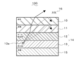
- FIG. 2 shows a structure of a conventional organic EL element (for example, see Non-Patent Document 1).
- the organic EL element 100 is formed by laminating an anode 11, an organic layer 14 including a hole transport layer 12 and a light emitting layer 13, and a cathode 15 in this order on a substrate 10.
- the surface of the substrate 10 opposite to the anode 11 is in contact with the atmosphere 16.
- the anode 11 injects holes into the light emitting layer 13
- the cathode 15 injects electrons into the light emitting layer 13, and these holes and electrons recombine in the light emitting layer 13.
- excitons are generated by this recombination, and when the excitons transition to the ground state, photons are emitted and taken out through the anode 11 and the substrate 10.
- the critical angle is determined from Snell's law at the interface based on the refractive index between the media, and has an incident angle greater than the critical angle.
- the light is totally reflected at the interface, confined in a medium having a high refractive index, and lost as guided light.
- the substrate 10 is exclusively made of glass from the viewpoints of excellent transparency, strength, low cost, gas barrier layer, chemical resistance, and heat resistance, and the refractive index of general soda lime glass is about 1.52. It is.
- ITO indium tin oxide
- IZO indium zinc oxide
- Their refractive index varies depending on the composition, film formation method, crystal structure, etc., but ITO is approximately 1.7 to 2.3, IZO is approximately 1.9 to 2.4, Very expensive.
- the refractive index of the light emitting material, electron transporting material, or hole transporting material used for the organic layer 14 is a ⁇ -conjugated bond material that contains a large number of general benzene rings in its molecular structure.
- the rate is about 1.6 to 2.0.
- the magnitude relationship of the refractive index of each layer is the atmosphere 16 ⁇ substrate 10 ⁇ organic layer 14 ⁇ anode 11 in contact with the substrate 10. Therefore, light emitted obliquely at a high angle from the light source 13a of the light emitting layer 13 in the organic layer 14 is totally reflected at the interface between the anode 11 and the substrate 10 and the interface between the substrate 10 and the atmosphere 16 (broken line). Indicated by an arrow).
- the refractive indexes of the atmosphere 16, the substrate 10, the anode 11, the hole transport layer 12, and the light emitting layer 13 are n 16 , n 10 , n 11 , n 12 , and n 13 , respectively.
- the incident angles from the light emitting layer 13 to the hole transport layer 12, from the hole transport layer 12 to the anode 11, from the anode 11 to the substrate 10, and from the substrate 10 to the atmosphere 16 are ⁇ 13-12 , ⁇ 12-11 , ⁇ 11-10 , respectively.
- ⁇ 10-16, and the emission angle from the substrate 10 to the atmosphere 16 is ⁇ 16 . From the Snell's law, the following equation 1 holds.
- the critical angles ⁇ c12 , ⁇ c10 , and ⁇ c16 of the hole transport layer 12, the substrate 10, and the atmosphere 16 viewed from the light emitting layer 13 are expressed by the following formulas 5 to 7, respectively. Desired.
- Light emitted from the light emitting source 13a of the light emitting layer 13 at the angle or more is confined in the light emitting layer 13, the anode 11 or the substrate 10 and becomes loss light. Therefore, the light extraction efficiency of the organic EL element 100 is lowered, and the external quantum efficiency is lowered.
- the light extraction efficiency is the ratio of photons generated in the light emitting layer and those photons that reach any layer or are emitted to the atmosphere.
- External quantum efficiency is the ratio of photons that reach any layer or are emitted to the atmosphere, relative to the number of electrons recombined in the emissive layer.
- the external quantum efficiency is obtained by multiplying the above-described light extraction efficiency by the internal quantum efficiency.
- Internal quantum efficiency is the ratio of generated photons to the number of electrons recombined in the emissive layer.
- Non-Patent Document 1 As a method of reducing the aforementioned loss light is low refractive index n 13 of the light emitting layer 13, thereby it is conceivable to increase the critical angle.
- SiO 2 is mixed with the light emitting layer 13 formed by MEH-PPV (poly [2-methoxy-5- (2′-ethyl-hexyloxy) -p-phenylene vinylene]). Techniques are shown. Since the refractive index of SiO 2 is 1.6 and lower than MEH-PPV, mixing the SiO 2 particles lowers the refractive index of the light emitting layer 13 and improves the quantum efficiency by 1.45 times. .
- the present invention has been made to solve the above-described conventional problems, and an object thereof is to provide an organic electroluminescence element capable of improving the light extraction efficiency.
- the electroluminescent device of the present invention is formed by laminating a substrate, a first electrode, an organic layer including a light emitting layer, and a second electrode in this order, and the light emitting layer is a mixture of porous particles in a light emitting material. It is characterized by being formed.
- the light emitting layer preferably has a refractive index lower than 1.6.
- the porous particles are preferably porous silica particles.
- the porous silica particles are preferably mesoporous silica nanoparticles.
- a plurality of mesopores having a pore diameter of 2 nm or more are arranged at equal intervals inside the mesoporous silica nanoparticles.
- the mesoporous silica nanoparticles preferably have a chain hydrocarbon structure on the surface.
- the surface of the mesoporous silica nanoparticles has an organic functional group having a ⁇ -conjugated bond.
- the porous particles preferably have a particle size of 10 to 100 nm.
- the light emitting material is preferably a coating type material.
- the organic electroluminescence device of the present invention since the light emitting layer is mixed with porous particles having a low refractive index and the refractive index is lowered, the critical angle at each interface existing in the optical path from the light emitting layer to the outside Can be increased. Therefore, it is possible to reduce the light that is totally reflected and lost at the interface between them and to increase the light extraction efficiency.
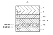
- FIG. 1 is a cross-sectional view of an organic EL device according to an embodiment of the present invention.
- FIG. 2 is a cross-sectional view of a conventional organic EL element.
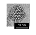
- FIG. 3 is a TEM observation of mesoporous silica particles in Example 1 of the present invention.
- FIG. 4 is a diagram showing an infrared absorption spectrum of mesoporous silica particles in Examples 1 to 3 of the present invention.
- FIG. 1 shows the configuration of the organic EL element of this embodiment.
- the organic EL element 1 is formed by laminating a first electrode 3, an organic layer 4, and a second electrode 5 on a substrate 2 in this order from the first electrode 3 side.
- the first electrode 3 is a light transmissive anode.
- the organic layer 4 has a hole injection layer 41, a hole transport layer 42, and a light emitting layer 43 in this order from the first electrode 3 side.
- the light emitting layer 43 is formed by mixing the light emitting material 44 with porous particles 45.
- the second electrode 5 is a light reflective cathode.
- a hole block layer, an electron transport layer, and an electron injection layer may be further stacked between the light emitting layer 43 and the second electrode 5.
- the first electrode 3 injects holes into the light emitting layer 43
- the second electrode 5 injects electrons into the light emitting layer 43. These holes and electrons are combined in the light emitting layer 43. Excitons are generated by this coupling, and light is emitted when the excitons transition to the ground state. This light is extracted outside through the first electrode 3 and the substrate 2.
- the substrate 2 is composed of a transparent glass plate, a transparent plastic film, a transparent plastic plate, or the like.
- a transparent glass soda lime glass or non-alkali glass is used.
- a polyester resin, a polyolefin resin, a polyamide resin, an epoxy resin, a fluorine resin, or the like is used.
- the substrate 2 may be a transparent glass plate mixed with heavy metals such as lead.
- the refractive index of the substrate 2 is about 1.52, for example.
- the first electrode 3 is an electrode for injecting holes into the light emitting layer 43, and is made of an electrode material having a work function of, for example, about 4 eV (electron volts) or more and a light transmittance of, for example, about 70% or more.
- This electrode material is made of conductive polymer such as CuI, ITO (indium-tin oxide), SnO 2 , ZnO, IZO (indium-zinc oxide), GZO (gallium-zinc oxide), PEDOT or polyaniline, or These can be formed of a conductive polymer doped with an acceptor.
- the first electrode 3 may be a transparent sheet in which a conductive material such as a metal such as gold, an alloy, or a carbon nanotube is dispersed.
- the sheet resistance of the first electrode 3 is preferably several hundred ⁇ / ⁇ or less, particularly preferably 100 ⁇ / ⁇ or less.
- the film thickness of the first electrode 3 is set to 500 nm or less, preferably in the range of 10 to 200 nm, although it depends on the electrode material in order to obtain the above characteristics such as light transmittance and sheet resistance.
- the hole injection layer 41 is composed of a low molecular weight organic compound such as copper phthalocyanine (CuPc) or a polymer material such as polyethylene dioxythiophene / polystyrene sulfonic acid (PEDOT-PSS).
- CuPc copper phthalocyanine
- PEDOT-PSS polyethylene dioxythiophene / polystyrene sulfonic acid
- the hole transport layer 42 comprises 4,4′-bis [N- (naphthyl) -N-phenyl-amino] biphenyl ( ⁇ -NPD), N, N′-bis (3-methylphenyl)-(1,1 ′ -Biphenyl) -4,4'-diamine (TPD), 2-TNATA, 4,4 ', 4 "-tris (N- (3-methylphenyl) N-phenylamino) triphenylamine (MTDATA), 4, 4'-N, N'-dicarbazole biphenyl (CBP), spiro-NPD, spiro-TPD, spiro-TAD, TNB, etc. as representative examples, triarylamine compounds, amine compounds containing carbazole groups, or fluorenes It is comprised by the amine compound containing a derivative.
- ⁇ -NPD 4,4′-bis [N- (naphthyl) -N-phenyl-amino] bi
- the hole injection layer 41 and the hole transport layer 42 may be formed by a dry process such as an evaporation method or a transfer method, or may be formed by a coating method such as spin coating, spray coating, die coating, or gravure printing. Also good.
- the light emitting material 44 of the light emitting layer 43 is a coating-type material, and the light emitting layer 43 is preliminarily mixed with porous particles 45 and formed into a film by a coating method such as spin coating, spray coating, die coating or gravure printing. Yes.
- the light emitting material 44 includes, for example, anthracene, naphthalene, pyrene, tetracene, coronene, perylene, phthaloperylene, naphthaloperylene, diphenylbutadiene, tetraphenylbutadiene, coumarin, oxadiazole, bisbenzoxazoline, bisstyryl, cyclopentadiene, quinoline metal complex, tris (8-hydroxyquinolinato) aluminum complex (Alq 3 ), tris (4-methyl-8-quinolinato) aluminum complex, tris (5-phenyl-8-quinolinato) aluminum complex, aminoquinoline metal complex, benzoquinoline metal complex , Tri- (p-terphenyl-4-yl) amine, 1-aryl-2,5-di (2-thienyl) pyrrole derivative, pyran, quinacridone, rubrene, distyrylbenzene derivative, distyle Ruariren derivatives, disty
- the light-emitting material 44 has, in a part of the molecule, a material that emits light by transitioning from the spin multiplet state to the ground state, such as a phosphorescent material, or the like. It may be a compound.
- the porous particles 45 are porous silica particles, and mesoporous silica is used as the porous silica. Hollow silica or nanoporous silica may be used as the porous silica.
- the material of the porous particles 45 is not limited to porous silica, and may be other metal oxides.
- the porous particles 45 have a low refractive index because air is contained in the voids in the particles. It is desirable that the porosity of the porous particles 45 be as high as possible.
- mesoporous silica as a porous material can have a higher porosity than hollow silica, the refractive index can be lowered.
- Mesoporous silica particles are preferred because the particle size can be controlled while maintaining the porosity. Furthermore, it has a feature that the dispersibility in other materials can be easily improved by forming an organic structure on the particle surface, which is particularly preferable.
- the organic structure on the surface of mesoporous silica is a chain hydrocarbon structure having 3 or more carbon atoms, an organic functional group having a ⁇ -conjugated bond, or the like.
- Examples of the chain hydrocarbon structure having 3 or more carbon atoms include saturated hydrocarbons, unsaturated hydrocarbons, and combinations thereof, which may be linear or branched, and cyclic hydrocarbons are part of the structure. Structures and atoms such as nitrogen and oxygen may be bonded.
- the organic functional group having a ⁇ -conjugated bond is not particularly limited as long as the ⁇ electron in the organic functional machine can be delocalized, but a functional group having a phenyl group, a naphthyl group, a styryl group, or a fluorene structure. And aryl groups thereof and derivatives thereof.
- the particle surface has the same functional group as the organic functional group contained in the light emitting material 44, it is particularly preferable because the dispersibility of the particle is easily improved.
- the average particle diameter of the porous particles 45 is approximately 10 to 100 nm when the thickness of the light emitting layer 43 is several tens nm to several hundreds nm. The average particle diameter is determined according to the thickness of the light emitting layer 43.
- the mesoporous silica particles as the porous particles 45 have the above particle diameter, they are also referred to as mesoporous silica nanoparticles or mesoporous silica fine particles.
- the mesoporous silica particles have a plurality of mesopores having a pore diameter of 2 nm or more inside.
- the mesopores in the particles often have regularity in arrangement, and are often arranged on two-dimensional hexagonals at regular intervals.
- the porosity of the mesoporous silica particles is a porosity in a plane perpendicular to the column direction of the cylindrical mesopores.
- the main peak obtained by X-ray diffraction measurement of mesoporous silica particles is 100 planes. 2 / ⁇ 3 times the calculated interplanar spacing d100 is the distance between the centers of adjacent meso holes.
- the peak value of the pore size distribution obtained by the nitrogen adsorption method is defined as the mesopore size.
- the porosity of mesoporous silica particles is the ratio of the cross-sectional area of the mesopores to the hexagonal area in which half the distance between adjacent mesopore centers is the distance of the opposite side, considering the symmetry of the mesopore arrangement.
- the porosity of the mesoporous silica particles as the porous particles 45 is approximately 20% or more and preferably 25% or more in such measurement.
- the method for producing mesoporous silica nanoparticles is not particularly limited, but mesoporous silica nanoparticles having an organic functional group on the particle surface and having mesopores having a two-dimensional hexagonal structure are, for example, non-patent documents Chem. Mater. 22, pp. 12 -14 (2010).
- the surfactant forms micelles while incorporating the hydrophobic part-containing additive into the hydrophobic part of the surfactant in water, and the micelles are regularly arranged.
- silicon alkoxide is added and subjected to a hydrolysis reaction using a base catalyst, a silica skeleton is formed in a particle shape so as to cover the outside of the micelle, and surfactant composite silica particles are generated.
- an organic functional group can be formed on the particles by using an organic functional group-containing silicon alkoxide such as an aminopropyl group.
- an organic functional group-containing silicon alkoxide such as an aminopropyl group.
- any organic functional group can be obtained. It can be formed on the particle surface. Furthermore, if the particle surface has a reactive functional group such as a silanol group, an amino group, an epoxy group, or a vinyl group, the desired organic functional group is bonded to the mesoporous silica nanoparticles via the reactive organic functional group. Can do.
- the light emitting layer 43 is formed by laminating a porous material 45 in advance in a light emitting material on a hole transport layer 42 which is a base layer of the light emitting layer 43.
- a light emitting layer 43 may be formed by laminating a light emitting material on a mesoporous silica film previously formed on the hole transport layer 42.
- the mesoporous silica film may be formed on the hole transport layer 42 by laminating the light emitting material 44 to a certain thickness, and the light emitting material 44 may be further laminated to form the light emitting layer 43 in which the mesoporous silica is mixed.
- the film thickness of the light emitting material 44 laminated in advance is preferably thin, for example, approximately 20 nm or less.
- the refractive index of the light emitting layer 43 is preferably lower than 1.6.
- the refractive index of the light emitting layer 43 is adjusted by selecting the light emitting material 44, selecting the material of the porous particles 45, adjusting the porosity, or the like.
- the second electrode 5 is an electrode for injecting electrons into the light emitting layer 43, and has a work function of, for example, about 5 eV or less.
- the second electrode 5 may be a light reflective electrode having light reflectivity for reflecting the light from the light emitting layer 43 in the direction of the substrate 2 or a light transmissive electrode for transmitting the above-described light.
- the reflectance is, for example, approximately 80% or more, and preferably 90% or more.
- the second electrode 5 is a light transmissive electrode
- the light transmittance is, for example, approximately 70% or more.
- the electrode material of the second electrode 5 is a metal, an alloy, an electrically conductive compound, or a mixture thereof.
- Specific electrode materials include alkali metals, alkali metal halides, alkali metal oxides, or alkaline earth metals, or alloys of these with other metals, such as sodium, sodium-potassium alloys, lithium, magnesium Magnesium-silver mixture, magnesium-indium mixture, aluminum-lithium alloy, Al / LiF mixture, and the like.
- Aluminum, silver (Ag), gold (Au), platinum (Pt), Al / Al 2 O 3 mixture, or the like can also be used as an electrode material.
- the electrode material may be one in which an alkali metal oxide, an alkali metal halide, or a metal oxide is used as the base of the second electrode 5 and one or more conductive materials such as metals are stacked thereon.
- the conductive material to be laminated is alkali metal / Al, alkali metal halide / alkaline earth metal / Al, alkali metal oxide / Al, or the like.
- an alkali metal such as lithium, sodium, cesium, or calcium, or an alkaline earth metal may be doped.
- the second electrode 5 is formed on the substrate 6 by a transparent electrode such as ITO or IZO in order to impart light transparency.
- the second electrode 5 may be formed by a combination of a transparent electrode and a light reflecting layer when having light reflectivity.
- Each of the electrodes 3 and 5 is formed by forming a thin film from the above-described electrical material by vacuum deposition, sputtering, coating, or the like.
- the film thickness of each electrode 3, 5 is set according to the material in order to make various characteristics such as the light transmittance of each electrode 3, 5 as described above, and is set to about 500 nm or less, for example.
- the film thickness is preferably within the range of about 10 to 200 nm.
- the sheet resistance of each of the electrodes 3 and 5 is several hundred ⁇ / ⁇ or less, but is preferably about 100 ⁇ / ⁇ or less.
- the substrate 2 was a non-alkali glass plate (No. 1737, manufactured by Corning) having a thickness of 0.7 mm.
- sputtering was performed on the substrate 2 using an ITO target (manufactured by Tosoh Corp.) to form an ITO layer having a thickness of 150 nm.
- the substrate 2 with the ITO layer was annealed at 200 ° C. for about 1 hour in an Ar atmosphere to form the first electrode 3 made of ITO and having a sheet resistance of 18 ⁇ / ⁇ .
- the refractive index of the first electrode 3 at a wavelength of 550 nm was 2.1 when measured with an optical thin film measurement system (“FilmTek” manufactured by SCI).
- PEDOT-PSS polyethylenedioxythiophene / polystyrene sulfonic acid
- the hole injection layer 41 was obtained by coating with a spin coater and baking at about 150 ° C. for 10 minutes.
- the refractive index of the hole injection layer 41 at a wavelength of 550 nm was 1.55 when measured in the same manner as the first electrode 3.
- TFB Poly [(9,9-dioctylfluorenyl-2,7-diyl) -co- (4,4 '-(N- (4-sec-butylphenyl)) diphenylamine)]
- a solution prepared by dissolving “Hole Transport Polymer ADS259BE” manufactured by American Dye Source Co., Ltd. in a THF solvent was applied on the hole injection layer 41 so as to have a film thickness of 12 nm using a spin coater, thereby producing a TFB coating.
- the hole transport layer 42 was obtained by baking this at 200 degreeC for 10 minute (s).
- the refractive index of the hole transport layer 42 at a wavelength of 550 nm was 1.64.
- a solution obtained by dissolving a red polymer ("Light Emitting Polymer ADS111RE" manufactured by American Dye Source) in a THF solvent as a light emitting material 44 is formed on the hole transport layer 42 using a spin coater so as to have a film thickness of 20 nm. This was applied and baked at 100 ° C. for 10 minutes. On top of that, a solution in which mesoporous silica particles as porous particles 45 prepared in advance were dispersed in butanol was applied, and further, red polymer ADS111RE was applied using a spin coater so that the total film thickness was 100 nm. Was baked at 100 ° C. for 10 minutes to obtain a light emitting layer 43. The refractive index of the light emitting layer 43 at a wavelength of 550 nm was 1.55.
- a second electrode 5 was produced by forming a film of Ba with a thickness of 5 nm and aluminum with a thickness of 80 nm on the light emitting layer 43 by a vacuum deposition method, and the organic EL element 1 was obtained.
- mesoporous silica particles as the porous particles 45 in Example 1 will be described.
- H 2 0 120 g, 25% NH 3 aqueous solution: 5.4 g
- ethylene glycol 20 g
- hexadecyltrimethylammonium bromide CTAB
- TMB 3,5-trimethylbenzene
- TEOS 1.29 g
- ⁇ -aminopropyltriethoxysilane 0.23 g
- Surfactant composite silica particles were obtained by stirring for a period of time.
- isopropanol: 30 g, 5N-HCl: 60 g, and hexamethyldisiloxane: 26 g are mixed and stirred at 72 ° C., and a synthetic reaction solution of surfactant composite silica particles is added, followed by stirring and refluxing for 30 minutes. did.
- the surfactant CTAB and the hydrophobic part-containing additive TMB were extracted from the surfactant composite silica particles to obtain mesoporous silica particles whose surface was trimethylsilylated.
- the solution after trimethylsilylation was centrifuged at 20,000 rpm for 20 minutes, and then the solution was removed.
- the mesoporous silica particles were washed by adding ethanol to the precipitated solid phase and shaking the particles in ethanol with a shaker. Centrifugation was performed at 20,000 rpm for 20 minutes, and the liquid was removed to obtain mesoporous silica particles.
- mesoporous silica particles dispersed in butanol were obtained.
- the particle size of the mesoporous silica particles was about 50 nm.
- Organic EL element 1 of Example 2 was obtained in the same manner as Example 1 except for the production method of mesoporous silica particles as porous particles 45.
- the refractive index of the light emitting layer 43 at a wavelength of 550 nm was 1.51.
- isopropanol 30 g
- 5N-HCl 60 g
- 1,3-di-n-octyltetramethyldioxane 57.4 g
- the reaction solution was added and stirred and refluxed for 30 minutes.
- the surfactant and the hydrophobic part-containing additive are extracted from the surfactant composite silica particles to obtain mesoporous silica particles in which octyl groups and methyl groups, which are hydrocarbons having 8 carbon atoms, are formed on the particle surface. It was.
- mesoporous silica particles dispersed in butanol were obtained from the prepared mesoporous silica particles.
- the particle size of the mesoporous silica particles was about 50 nm.
- a solution prepared by dissolving a red polymer ("Light Emitting Polymer ADS111RE" manufactured by American Dye Source Co., Ltd.) and previously prepared mesoporous silica particles in a THF solvent at a weight ratio of 1: 1 is formed on the hole transport layer 42 to a film thickness of 100 nm. It applied so that it might become. By firing this at 100 ° C. for 10 minutes, a light emitting layer 43 was obtained. Other than that was carried out similarly to Example 1, and obtained the organic EL element 1.
- Example 3 Preparation of mesoporous silica particles in Example 3 will be described. First, surfactant composite silica particles were obtained in the same manner as in Example 1.
- isopropanol 30 g
- 5N-HCl 60 g
- 1,3-diphenyltetramethyldisiloxane 45.8 g
- the surfactant composite silica particle synthesis reaction solution was added. And stirred and refluxed for 30 minutes.
- the surfactant and the hydrophobic part-containing additive were extracted from the surfactant composite silica particles to obtain mesoporous silica particles in which phenyl groups and methyl groups were formed on the particle surfaces.
- mesoporous silica particles dispersed in butanol were obtained from the prepared mesoporous silica particles.
- the particle size of the mesoporous silica particles was about 50 nm.
- Organic EL element 1 of Example 4 was obtained in the same manner as Example 1 except for the production method of mesoporous silica particles as porous particles 45.
- the refractive index of the light emitting layer 43 at a wavelength of 550 nm was 1.51.
- mesoporous silica particles as the porous particles 45 in Example 4 will be described.
- mesoporous silica particles were recovered from the liquid after trimethylsilylation by centrifugation and dispersed in 10 g of toluene.
- 2 g of epoxy group-containing fluorene (Ogsol EG200, manufactured by Osaka Gas Chemical Co., Ltd.) was added to this solution, and the mixture was stirred at room temperature for 12 hours to react an epoxy group with the amino group on the mesoporous silica surface, thereby binding the fluorene structure to the surface.
- the liquid after the reaction was centrifuged to collect the particles, which were redispersed by shaking in 1-butanol.
- the prepared mesoporous silica particles of Examples 1 to 4 were dried and subjected to transmission electron microscope observation (TEM), nitrogen adsorption measurement, and FT-IR measurement.
- TEM transmission electron microscope observation
- nitrogen adsorption measurement nitrogen adsorption measurement
- FT-IR measurement FT-IR measurement
- Example 1 The microstructure of the mesoporous silica particles of Example 1 was observed with a TEM using JEM 2000EXII (manufactured by JEOL). The TEM image of Example 1 is shown in FIG. It was confirmed that the mesopores formed a two-dimensional hexagonal structure. Similar results were obtained for the mesoporous silica particles of Examples 2 to 4.
- FIG. 4 shows infrared absorption spectra of the mesoporous silica particles obtained in Examples 1 to 3. Each spectrum describes the characteristic absorption. As shown in the spectrum, in Example 1, a trimethylsilyl group (Si— (CH 3 ) 3 ) was confirmed, and in Example 2, an increase in the peak of CH 2 was confirmed as compared with Example 1, indicating the presence of an octyl group.
- Example 3 the peak of the trimethylsilyl group disappeared, and (Si— (CH 3 ) 2 ) was observed, suggesting that an octyl group and a methyl group were formed.
- the phenyl group was confirmed and the peak of the trimethylsilyl group disappeared, and (Si— (CH 3 ) 2 ) was observed, suggesting that a phenyl group and a methyl group were formed. It was done. This confirmed that mesoporous silica fine particles having various organic functional groups on the surface were formed by the organosilicon compound containing a siloxane bond in the molecule.
- Comparative Example 1 An organic EL device of Comparative Example 1 was obtained in the same manner as in Example 1 except that the porous particles 45 were not mixed in the light emitting layer 43.
- the refractive index of the light emitting layer 43 at a wavelength of 550 nm was 1.67.
- Comparative Example 2 An organic EL device of Comparative Example 2 was obtained in the same manner as in Example 1 except that the porous particles mixed in the light emitting layer 43 were SiO 2 particles. In this organic EL element, the refractive index of the light emitting layer 43 at a wavelength of 550 nm was 1.65.
- the organic EL elements 1 of Examples 1 to 4 in which the porous particles 45 were mesoporous silica particles were used in Comparative Example 1 in which the porous particles 45 were not mixed, and the porous particles
- the external quantum efficiency was higher than that of Comparative Example 2 in which 45 was SiO 2 particles.
- the refractive index of the light emitting layer 43 was lower and the external quantum efficiency was higher than that of Example 1.
- the light emitting layer 43 is mixed with the low-refractive-index porous particles 45 to lower the refractive index. Therefore, at each interface present in the optical path from the light emitting layer 43 to the outside. The critical angle of can be increased. Therefore, it is possible to reduce the light that is totally reflected at the interface and lost. For this reason, the light extraction efficiency to the substrate 2 and the atmosphere can be increased, and the external quantum efficiencies of the substrate arrival light and the atmospheric radiation light can be increased as shown in the evaluation test results.
- the refractive index of the light emitting layer 43 is 1.6 or less, the light extraction layer 43 can be made lower than before, and the light extraction efficiency of the organic EL element 1 can be improved.
- porous particles 45 porous silica particles, since the porous silica has a low refractive index, the refractive index of the light emitting layer 43 can be lowered, and the light extraction efficiency of the organic EL element 1 can be improved. .
- mesoporous silica particles as the porous silica particles, since mesoporous silica has a lower refractive index than hollow silica, the refractive index of the light emitting layer 43 can be lowered, and the light extraction efficiency of the organic EL element 1 can be improved.
- a plurality of mesopores having a pore diameter of 2 nm or more are arranged at equal intervals, so that the porosity can be increased and the refractive index can be decreased. Thereby, the refractive index of the light emitting layer 43 can be made low, and the light extraction efficiency of the organic EL element 1 can be improved.
- the mesoporous silica particles have a chain hydrocarbon structure on the surface, the particles repel each other and can be uniformly dispersed.
- the light emitting material 44 of the light emitting layer 43 is a ⁇ -conjugated bond material containing a large number of general benzene rings in its molecular structure. For this reason, mesoporous silica particles have a ⁇ -conjugated phenyl group or a fluorene structure on the surface, so that they are easily mixed with the light emitting material 44.
- the porous particles 45 have a particle diameter of 10 to 100 nm and are not too large. Therefore, the density of the porous particles 45 in the light emitting layer 43 can be increased, and the refractive index of the light emitting layer 43 can be further lowered. Can do. In addition, since the particle size is not too small, the density of the porous particles 45 does not become too high and the light emission amount of the light emitting layer 43 does not decrease.
- the porous particles 45 can be mixed with the light emitting material 44 in advance to form a film. Therefore, the density unevenness of the porous particles 45 can be eliminated. For this reason, the refractive index of the light emitting layer 43 can be made uniform, and unevenness in light can be eliminated.
- the organic EL element 1 may have a plurality of light emitting layers 43.
- the plurality of organic layers 4 including the first electrode 3 and the light emitting layer 43 are disposed on the substrate 2 via the charge supply layer.
- the second electrode 5 is formed thereon.
- the charge supply layer is made of, for example, a metal thin film such as Ag, Au, or Al, a metal oxide such as vanadium oxide, molybdenum oxide, rhenium oxide, or tungsten oxide, or a transparent conductive material such as ITO, IZO, AZO, GZO, ATO, or SnO 2.
- n-type semiconductor and p-type semiconductor laminate metal thin film or transparent conductive film and n-type semiconductor and / or p-type semiconductor, n-type semiconductor and p-type semiconductor mixture, n-type semiconductor and / Or a mixture of a p-type semiconductor and a metal.
- the n-type semiconductor or p-type semiconductor may be an inorganic material or an organic material, a mixture of an organic material and a metal, an organic material and a metal oxide, an organic material and an organic acceptor / donor material, an inorganic material Any combination of the system acceptor / donor materials may be used.
- a plurality of light emitting layers 43 may be laminated in one organic layer 4.
- the number of stacked layers is not particularly limited. However, when the number of layers increases, the difficulty of optical and electrical element design increases. Particularly preferred.
- the light emitting layer 43 may be formed by a dry process such as a vapor deposition method or a transfer method.
- the organic layer 4 can be configured by appropriately stacking organic layers such as an electron injection layer, an electron transport layer, a hole block layer, a hole injection layer, and a hole transport layer on the light emitting layer 43 as necessary.
- the material is a metal complex known as an electron transport material such as Alq 3 , a compound having a hetero ring such as a phenanthroline derivative, a pyridine derivative, a tetrazine derivative, or an oxadiazole derivative, etc. Those having a high charge transporting property are desirable.
- the first electrode 3 may be a cathode and the second electrode 5 may be an anode.
- Organic electroluminescence device organic EL device
- Substrate First electrode (anode)
- Organic layer Light-emitting layer
- Light-emitting material 45
- Porous particles 5
Landscapes
- Physics & Mathematics (AREA)
- Optics & Photonics (AREA)
- Chemical & Material Sciences (AREA)
- Engineering & Computer Science (AREA)
- Materials Engineering (AREA)
- Organic Chemistry (AREA)
- Electroluminescent Light Sources (AREA)
Priority Applications (3)
| Application Number | Priority Date | Filing Date | Title |
|---|---|---|---|
| CN2010800239192A CN102460764A (zh) | 2009-06-02 | 2010-06-02 | 有机电致发光元件 |
| EP10783411.1A EP2439805B1 (en) | 2009-06-02 | 2010-06-02 | Organic electroluminescent element |
| US13/375,586 US8921833B2 (en) | 2009-06-02 | 2010-06-02 | Organic electroluminescent element |
Applications Claiming Priority (4)
| Application Number | Priority Date | Filing Date | Title |
|---|---|---|---|
| JP2009133020 | 2009-06-02 | ||
| JP2009-133020 | 2009-06-02 | ||
| JP2010-125639 | 2010-06-01 | ||
| JP2010125639A JP5658913B2 (ja) | 2009-06-02 | 2010-06-01 | 有機エレクトロルミネッセンス素子 |
Publications (1)
| Publication Number | Publication Date |
|---|---|
| WO2010140629A1 true WO2010140629A1 (ja) | 2010-12-09 |
Family
ID=43297762
Family Applications (1)
| Application Number | Title | Priority Date | Filing Date |
|---|---|---|---|
| PCT/JP2010/059368 Ceased WO2010140629A1 (ja) | 2009-06-02 | 2010-06-02 | 有機エレクトロルミネッセンス素子 |
Country Status (6)
| Country | Link |
|---|---|
| US (1) | US8921833B2 (enExample) |
| EP (1) | EP2439805B1 (enExample) |
| JP (1) | JP5658913B2 (enExample) |
| KR (1) | KR20120024639A (enExample) |
| CN (1) | CN102460764A (enExample) |
| WO (1) | WO2010140629A1 (enExample) |
Cited By (9)
| Publication number | Priority date | Publication date | Assignee | Title |
|---|---|---|---|---|
| US20120164334A1 (en) * | 2008-08-26 | 2012-06-28 | Snu R&Db Foundation | Article treated with silica particles and method for treating a surface of the article |
| CN102842686A (zh) * | 2011-06-21 | 2012-12-26 | 卡帝瓦公司 | 用于控制有机发光器件的性质的材料和方法 |
| US20120326139A1 (en) * | 2011-06-21 | 2012-12-27 | Kateeva, Inc. | Materials and methods for controlling properties of organic light-emitting device |
| CN103620807A (zh) * | 2011-06-21 | 2014-03-05 | 科迪华公司 | 用于oled微腔和缓冲层的材料和方法 |
| CN103828084A (zh) * | 2011-09-30 | 2014-05-28 | 通用电气公司 | 包括中空物体的oled装置 |
| JP2014207443A (ja) * | 2013-03-20 | 2014-10-30 | 株式会社半導体エネルギー研究所 | 発光モジュール、発光装置 |
| US8921833B2 (en) | 2009-06-02 | 2014-12-30 | Panasonic Corporation | Organic electroluminescent element |
| CN104303328A (zh) * | 2012-03-23 | 2015-01-21 | 株式会社Lg化学 | 有机发光器件 |
| CN104466019A (zh) * | 2014-11-25 | 2015-03-25 | 上海交通大学 | 提高光萃取效率的结构及其方法 |
Families Citing this family (10)
| Publication number | Priority date | Publication date | Assignee | Title |
|---|---|---|---|---|
| JP5776079B2 (ja) | 2010-02-26 | 2015-09-09 | 日東電工株式会社 | ビソプロロール含有貼付製剤 |
| JP2012222013A (ja) * | 2011-04-05 | 2012-11-12 | Panasonic Corp | 有機薄膜及びこれを発光層に含む有機エレクトロルミネッセンス素子 |
| JP2013004741A (ja) * | 2011-06-16 | 2013-01-07 | Toshiba Corp | 半導体発光素子 |
| US8828533B2 (en) * | 2012-01-12 | 2014-09-09 | Ut-Battelle, Llc | Mesoporous carbon materials |
| JPWO2014024379A1 (ja) * | 2012-08-10 | 2016-07-25 | パナソニックIpマネジメント株式会社 | メソポーラスシリカ微粒子、メソポーラスシリカ微粒子の製造方法、メソポーラスシリカ微粒子含有組成物、メソポーラスシリカ微粒子含有成形物及び有機エレクトロルミネッセンス素子 |
| CN103738970B (zh) * | 2013-12-25 | 2015-06-24 | 上海纳米技术及应用国家工程研究中心有限公司 | 高透过率纳米多孔气凝胶材料及其制备方法 |
| KR102589906B1 (ko) * | 2016-10-31 | 2023-10-13 | 엘지디스플레이 주식회사 | 유기발광 표시장치 |
| WO2020045412A1 (ja) * | 2018-08-28 | 2020-03-05 | コニカミノルタ株式会社 | 有機エレクトロルミネッセンス素子及びその製造方法 |
| CN109585666A (zh) * | 2018-12-04 | 2019-04-05 | 惠科股份有限公司 | 一种显示面板、显示面板的制造方法和显示装置 |
| KR102664869B1 (ko) * | 2020-12-17 | 2024-05-17 | 한국전자통신연구원 | 표시 장치 |
Citations (2)
| Publication number | Priority date | Publication date | Assignee | Title |
|---|---|---|---|---|
| JP2007242927A (ja) * | 2006-03-09 | 2007-09-20 | Seiko Epson Corp | 発光装置及び発光装置の製造方法 |
| JP2007266243A (ja) * | 2006-03-28 | 2007-10-11 | Canon Inc | 有機発光素子 |
Family Cites Families (8)
| Publication number | Priority date | Publication date | Assignee | Title |
|---|---|---|---|---|
| JP2000188183A (ja) * | 1998-12-22 | 2000-07-04 | Oputeku:Kk | ディスプレイデバイス及びディスプレイデバイスの製造方法 |
| WO2004112440A1 (ja) * | 2003-06-13 | 2004-12-23 | Matsushita Electric Industrial Co., Ltd. | 発光素子及びその製造方法、表示装置 |
| CN100484351C (zh) * | 2003-06-13 | 2009-04-29 | 松下电器产业株式会社 | 发光元件及其制造方法、显示装置 |
| JP4640711B2 (ja) * | 2004-03-25 | 2011-03-02 | 株式会社豊田中央研究所 | 発光材料及びその製造方法 |
| ES2251882B1 (es) * | 2004-10-21 | 2007-06-16 | Universidad Politecnica De Valencia | Material electroluminiscente que esta constituido por un solido microporoso o mesoporoso conteniendo compuestos organicos covalentemente enlazados que confieren propiedades elctroluminescentes. |
| JP4844030B2 (ja) * | 2005-07-15 | 2011-12-21 | セイコーエプソン株式会社 | 発光素子および電子機器 |
| US7795625B2 (en) * | 2006-01-16 | 2010-09-14 | Panasonic Corporation | Semiconductor light-emitting device |
| JP5658913B2 (ja) | 2009-06-02 | 2015-01-28 | パナソニックIpマネジメント株式会社 | 有機エレクトロルミネッセンス素子 |
-
2010
- 2010-06-01 JP JP2010125639A patent/JP5658913B2/ja active Active
- 2010-06-02 CN CN2010800239192A patent/CN102460764A/zh active Pending
- 2010-06-02 EP EP10783411.1A patent/EP2439805B1/en active Active
- 2010-06-02 US US13/375,586 patent/US8921833B2/en active Active
- 2010-06-02 KR KR1020117027923A patent/KR20120024639A/ko not_active Ceased
- 2010-06-02 WO PCT/JP2010/059368 patent/WO2010140629A1/ja not_active Ceased
Patent Citations (2)
| Publication number | Priority date | Publication date | Assignee | Title |
|---|---|---|---|---|
| JP2007242927A (ja) * | 2006-03-09 | 2007-09-20 | Seiko Epson Corp | 発光装置及び発光装置の製造方法 |
| JP2007266243A (ja) * | 2006-03-28 | 2007-10-11 | Canon Inc | 有機発光素子 |
Non-Patent Citations (3)
| Title |
|---|
| CARTER, S. A. ET AL.: "Enhanced luminance in polymer composite light emitting devices", APPLIED PHYSICS LETTERS, vol. 71, no. 9, 1997, pages 1145, XP000720223, DOI: doi:10.1063/1.119848 |
| CHEM. MATER. 22, 2010, pages 12 - 14 |
| See also references of EP2439805A4 |
Cited By (13)
| Publication number | Priority date | Publication date | Assignee | Title |
|---|---|---|---|---|
| US20120164334A1 (en) * | 2008-08-26 | 2012-06-28 | Snu R&Db Foundation | Article treated with silica particles and method for treating a surface of the article |
| US8921833B2 (en) | 2009-06-02 | 2014-12-30 | Panasonic Corporation | Organic electroluminescent element |
| US8809079B2 (en) | 2011-06-21 | 2014-08-19 | Kateeva, Inc. | Materials and methods for organic light-emitting device microcavity |
| US20120326136A1 (en) * | 2011-06-21 | 2012-12-27 | Kateeva, Inc. | Materials and methods for controlling properties of organic light-emitting device |
| CN103620807A (zh) * | 2011-06-21 | 2014-03-05 | 科迪华公司 | 用于oled微腔和缓冲层的材料和方法 |
| US20120326139A1 (en) * | 2011-06-21 | 2012-12-27 | Kateeva, Inc. | Materials and methods for controlling properties of organic light-emitting device |
| CN102842686A (zh) * | 2011-06-21 | 2012-12-26 | 卡帝瓦公司 | 用于控制有机发光器件的性质的材料和方法 |
| US9012892B2 (en) | 2011-06-21 | 2015-04-21 | Kateeva, Inc. | Materials and methods for controlling properties of organic light-emitting device |
| CN103828084A (zh) * | 2011-09-30 | 2014-05-28 | 通用电气公司 | 包括中空物体的oled装置 |
| CN104303328A (zh) * | 2012-03-23 | 2015-01-21 | 株式会社Lg化学 | 有机发光器件 |
| US9577224B2 (en) | 2012-03-23 | 2017-02-21 | Lg Display Co., Ltd. | Organic light emitting device |
| JP2014207443A (ja) * | 2013-03-20 | 2014-10-30 | 株式会社半導体エネルギー研究所 | 発光モジュール、発光装置 |
| CN104466019A (zh) * | 2014-11-25 | 2015-03-25 | 上海交通大学 | 提高光萃取效率的结构及其方法 |
Also Published As
| Publication number | Publication date |
|---|---|
| JP2011014534A (ja) | 2011-01-20 |
| EP2439805B1 (en) | 2020-08-05 |
| US20120068171A1 (en) | 2012-03-22 |
| JP5658913B2 (ja) | 2015-01-28 |
| EP2439805A1 (en) | 2012-04-11 |
| KR20120024639A (ko) | 2012-03-14 |
| CN102460764A (zh) | 2012-05-16 |
| US8921833B2 (en) | 2014-12-30 |
| EP2439805A4 (en) | 2013-08-21 |
Similar Documents
| Publication | Publication Date | Title |
|---|---|---|
| JP5658913B2 (ja) | 有機エレクトロルミネッセンス素子 | |
| Zou et al. | Recent advances in organic light-emitting diodes: toward smart lighting and displays | |
| US9257675B2 (en) | Substrate for an organic electronic device and an organic electronic device comprising the same | |
| Liu et al. | Toward see‐through optoelectronics: Transparent light‐emitting diodes and solar cells | |
| JP5824678B2 (ja) | 有機エレクトロルミネッセンス素子 | |
| US8455896B2 (en) | Organic LED and manufacturing method thereof | |
| US20080238310A1 (en) | OLED with improved light outcoupling | |
| Tong et al. | Efficient light extraction of organic light‐emitting diodes on a fully solution‐processed flexible substrate | |
| CN108630820A (zh) | 一种交流平面有机电致发光器件 | |
| KR20140024307A (ko) | 조명용 유기 전자 소자 | |
| CN103460430B (zh) | 有机el元件及其制造方法 | |
| CN107331783B (zh) | 一种自由基双重态敏化荧光有机电致发光器件 | |
| TWI668893B (zh) | 有機電發光裝置 | |
| JP5933495B2 (ja) | 有機電界発光素子及び有機電界発光素子の製造方法 | |
| TWI657608B (zh) | 有機發光裝置 | |
| CN111200076A (zh) | 具有内部光提取结构的有机发光器件及其制备方法 | |
| Xue et al. | Highly flexible light emitting diodes based on a quantum dots-polymer composite emitting layer | |
| JP2011154843A (ja) | 有機エレクトロルミネッセンス素子 | |
| JP2012009336A (ja) | 有機エレクトロルミネッセンス素子 | |
| WO2012176692A1 (ja) | 有機エレクトロルミネッセンス素子及びその製造方法 | |
| JP2012119524A (ja) | 有機エレクトロルミネッセンス素子 | |
| JP2013089501A (ja) | 有機エレクトロルミネッセンス素子 | |
| Peng et al. | Doping core–shell nanoparticles into a solution-processed electron transporting layer for polymer light-emitting diodes | |
| JP2011048999A (ja) | 有機エレクトロルミネッセンス素子 | |
| JP2012248696A (ja) | 有機エレクトロルミネッセンス素子 |
Legal Events
| Date | Code | Title | Description |
|---|---|---|---|
| WWE | Wipo information: entry into national phase |
Ref document number: 201080023919.2 Country of ref document: CN |
|
| 121 | Ep: the epo has been informed by wipo that ep was designated in this application |
Ref document number: 10783411 Country of ref document: EP Kind code of ref document: A1 |
|
| ENP | Entry into the national phase |
Ref document number: 20117027923 Country of ref document: KR Kind code of ref document: A |
|
| WWE | Wipo information: entry into national phase |
Ref document number: 2010783411 Country of ref document: EP |
|
| WWE | Wipo information: entry into national phase |
Ref document number: 13375586 Country of ref document: US |
|
| NENP | Non-entry into the national phase |
Ref country code: DE |