WO2010134229A1 - 窒化物半導体発光装置 - Google Patents
窒化物半導体発光装置 Download PDFInfo
- Publication number
- WO2010134229A1 WO2010134229A1 PCT/JP2010/000262 JP2010000262W WO2010134229A1 WO 2010134229 A1 WO2010134229 A1 WO 2010134229A1 JP 2010000262 W JP2010000262 W JP 2010000262W WO 2010134229 A1 WO2010134229 A1 WO 2010134229A1
- Authority
- WO
- WIPO (PCT)
- Prior art keywords
- film
- light emitting
- protective film
- nitride semiconductor
- aln
- Prior art date
Links
Images


Classifications
-
- H—ELECTRICITY
- H01—ELECTRIC ELEMENTS
- H01S—DEVICES USING THE PROCESS OF LIGHT AMPLIFICATION BY STIMULATED EMISSION OF RADIATION [LASER] TO AMPLIFY OR GENERATE LIGHT; DEVICES USING STIMULATED EMISSION OF ELECTROMAGNETIC RADIATION IN WAVE RANGES OTHER THAN OPTICAL
- H01S5/00—Semiconductor lasers
- H01S5/30—Structure or shape of the active region; Materials used for the active region
- H01S5/32—Structure or shape of the active region; Materials used for the active region comprising PN junctions, e.g. hetero- or double- heterostructures
- H01S5/323—Structure or shape of the active region; Materials used for the active region comprising PN junctions, e.g. hetero- or double- heterostructures in AIIIBV compounds, e.g. AlGaAs-laser, InP-based laser
- H01S5/32308—Structure or shape of the active region; Materials used for the active region comprising PN junctions, e.g. hetero- or double- heterostructures in AIIIBV compounds, e.g. AlGaAs-laser, InP-based laser emitting light at a wavelength less than 900 nm
- H01S5/32341—Structure or shape of the active region; Materials used for the active region comprising PN junctions, e.g. hetero- or double- heterostructures in AIIIBV compounds, e.g. AlGaAs-laser, InP-based laser emitting light at a wavelength less than 900 nm blue laser based on GaN or GaP
-
- H—ELECTRICITY
- H01—ELECTRIC ELEMENTS
- H01S—DEVICES USING THE PROCESS OF LIGHT AMPLIFICATION BY STIMULATED EMISSION OF RADIATION [LASER] TO AMPLIFY OR GENERATE LIGHT; DEVICES USING STIMULATED EMISSION OF ELECTROMAGNETIC RADIATION IN WAVE RANGES OTHER THAN OPTICAL
- H01S5/00—Semiconductor lasers
- H01S5/02—Structural details or components not essential to laser action
- H01S5/028—Coatings ; Treatment of the laser facets, e.g. etching, passivation layers or reflecting layers
- H01S5/0281—Coatings made of semiconductor materials
-
- H—ELECTRICITY
- H01—ELECTRIC ELEMENTS
- H01S—DEVICES USING THE PROCESS OF LIGHT AMPLIFICATION BY STIMULATED EMISSION OF RADIATION [LASER] TO AMPLIFY OR GENERATE LIGHT; DEVICES USING STIMULATED EMISSION OF ELECTROMAGNETIC RADIATION IN WAVE RANGES OTHER THAN OPTICAL
- H01S5/00—Semiconductor lasers
- H01S5/02—Structural details or components not essential to laser action
- H01S5/028—Coatings ; Treatment of the laser facets, e.g. etching, passivation layers or reflecting layers
- H01S5/0282—Passivation layers or treatments
- H01S5/0283—Optically inactive coating on the facet, e.g. half-wave coating
Definitions
- the present invention relates to a nitride semiconductor light emitting device, and more particularly to a nitride semiconductor light emitting device in which a protective film is provided on a light emitting facet.
- the semiconductor laser device is a light source for reproducing and recording optical disc media represented by a compact disc (CD), a digital versatile disc (DVD), a Blu-ray Disc (registered trademark) and the like.
- CD compact disc
- DVD digital versatile disc
- Blu-ray Disc registered trademark
- high-speed information recording operation is required, and in order to record a large amount of information in a short time, high output of the semiconductor laser device is indispensable.
- the deterioration phenomenon in which the operating current gradually increases when the light output increases and the phenomenon in which the semiconductor laser device does not oscillate due to a phenomenon called optical destruction. Therefore, in order to realize high output, research and development for suppressing or preventing such deterioration of the semiconductor laser device is actively made. In particular, since drowning with optical destruction occurs at the front end face which is the light emission surface of the laser resonator, efforts have been made to make the protective film covering the resonator end face robust and stable. In general, the resonator end face of the semiconductor laser device is covered with a protective film, and performs control of reflectance on the resonator end face, prevention of foreign matter adhesion, and oxidation prevention of the resonator end face.
- FIG. 16 shows a schematic cross-sectional configuration of the conventional nitride semiconductor laser device described in Patent Document 1.
- the conventional nitride semiconductor laser device comprises a laser structure 100 comprising an active layer (light emitting layer) 102 and an n-type semiconductor layer 101 and a p-type semiconductor layer 103 sandwiching the active layer 102.
- a p-side electrode 104 is formed on the p-type semiconductor layer 103
- an n-side electrode 105 is formed on the n-type semiconductor layer 101.
- a protective film 106 made of a metal oxide such as silicon oxide (SiO 2 ) or aluminum oxide (Al 2 O 3 ) is provided on the rear end surface of the laser structure 100 that functions as a mirror of the resonator.
- a metal oxide such as silicon oxide (SiO 2 ) or aluminum oxide (Al 2 O 3 )
- AlN aluminum nitride
- Al 2 O 3 aluminum oxide
- one of the causes of deterioration of the semiconductor laser device in increasing the output is the solid phase reaction between the first protective film 107 or the like and the end face of the semiconductor caused by the heat generation and light absorption of the laser structure 100, and each protection It is considered that an interface reaction at the facet of the resonator, such as residual oxygen in the film or oxygen in the package diffuses in the protective film and oxidizes the facet of the resonator as the laser oscillates.
- each protective film is peeled off from the laser structure 100 or a crack or the like is generated in the laser structure 100 to cause physical destruction.
- AlN which is the conventional first protective film 107 shown in FIG. 16, is a crystalline thin film, it is robust, has good thermal conductivity, and is an extremely excellent material as an end face coat film.
- AlN is a nitride like a nitride semiconductor, a solid phase reaction with the laser structure 100 is also suppressed.
- the AlN film has a large film stress, and a crack is easily generated due to the laser oscillation operation.
- AlN has a light absorption band due to a defect or the like in the vicinity of a wavelength of 400 nm, and it is thought that light absorption at the time of laser oscillation causes heat generation and diffusion of oxygen.
- Patent Document 2 describes the structure of an AlN film and the film forming method for reducing the film stress.
- film stress is relaxed by laminating AlN films having crystal orientations different from each other, and cracking and film peeling due to heat generation are suppressed.
- Patent Document 3 describes a configuration in which AlN added with a rare earth element is used as a protective film in order to suppress the diffusion of oxygen.
- the rare earth element combines with oxygen, which makes it possible to suppress the diffusion of oxygen.
- an AlN film to which such a rare earth element is added By using an AlN film to which such a rare earth element is added, oxidation and film peeling of the facets of the resonator are prevented, and optical breakdown and deterioration of the facets are suppressed, compared with the case of using a normal AlN film. Laser operation is possible.
- the AlN film described in Patent Document 2 can suppress the occurrence of film peeling and cracking, it has a problem that optical breakdown occurs due to heat generation of the end surface or oxidation of the end surface caused by light absorption.
- Patent Document 2 since AlN films having different crystal orientations are stacked, an interface is generated between AlN films having different crystal orientations, which is the source of light absorption.
- the AlN film of Patent Document 1 is polycrystalline, and light absorption occurs at the interface between grains. Such light absorption by the AlN film causes heat generation at the facets of the resonator and diffusion of oxygen in the AlN film, leading to optical destruction, and thus causes a decrease in the reliability of the semiconductor laser device.
- An object of the present invention is to solve the above-mentioned problems and to obtain an end face protective film which does not absorb light at high output operation and does not cause optical destruction.
- the present invention uses a nitride semiconductor light emitting device using a crystalline film made of a nitride containing aluminum as an end face protective film, and the crystalline film has a predetermined size and a crystal orientation plane. Is formed by an assembly of domains in which the inclination angle and the rotation angle are the same as each other. The definition of the domain will be described later.
- the first nitride semiconductor light-emitting device is formed of a group III nitride semiconductor, and is formed so as to cover a semiconductor stack having a light emitting end face and a light emitting end face of the semiconductor stack.
- the first protective film is a crystalline film made of a nitride containing aluminum, and the crystalline film has a plurality of domains in which the tilt angle and the rotation angle in the crystal orientation plane are the same as each other.
- the boundary length of each domain per unit area is 7 ⁇ m ⁇ 1 or less.
- the first protective film having crystallinity which is a nitride containing aluminum, has a boundary length of 7 ⁇ m ⁇ 1 or less per unit area, That is, the area of a single domain is large. As a result, the area of the interface between the domains per unit area is reduced and light absorption is reduced, so that heat generation and diffusion of oxygen during operation can be suppressed. As a result, a nitride semiconductor light emitting device having a high output and a long life can be realized.
- a second nitride semiconductor light-emitting device comprises a semiconductor laminate comprising a group III nitride semiconductor and having a light-emitting end face, and a first protective film formed to cover the light-emitting end face of the semiconductor laminate.
- the first protective film is a crystalline film made of a nitride containing aluminum, and the crystalline film is an assembly of a plurality of domains in which the tilt angle and the rotation angle in the crystal orientation plane are the same as each other.
- the area of the domain facing the light transmission region of the light emitting end face among the plurality of domains is larger than the area of the light transmission region.
- the crystalline first protective film made of a nitride containing aluminum is an aggregate of a plurality of domains in which the tilt angle and the rotation angle in the crystal orientation plane are the same as each other.
- the area of the domain facing the light transmission region of the light emitting end face is larger than the area of the light transmission region. Therefore, the light emission light emitted from the light emission end face is not absorbed or scattered by the interface between the domains. Therefore, heat generation during operation and light loss due to diffusion and scattering of oxygen can be suppressed more reliably, so that a nitride semiconductor light emitting device with high output and long life can be realized.
- the first protective film preferably has a single domain in which both the tilt angle and the rotation angle in the crystal orientation plane are within 2 °.
- the first protective film may have a crystal structure having the same crystal axis orientation as that of the semiconductor stack.
- the film stress that the first protective film exerts on the semiconductor stack can be reduced, so that it is possible to prevent film peeling and cracking of the first protective film.
- the first protective film may have a crystal structure having a crystal axis orientation different from that of the semiconductor stack.
- the light absorption coefficient of the first protective film can be made smaller.
- the crystal structure of the semiconductor stack may be hexagonal, the light emitting end face may be m-plane, and the first protective film may be c-axis aligned.
- the first or second nitride semiconductor light emitting device further includes a second protective film formed to cover the first protective film, and the second protective film is an amorphous film containing oxygen. May be
- the nitride semiconductor light emitting device can obtain an end face protective film which has little light absorption even at the time of high power operation and does not cause optical destruction, and therefore can realize long life and high reliability.
- FIG. 1A and FIG. 1B are schematic cross-sectional views in the order of steps showing the method for manufacturing a nitride semiconductor light emitting device according to the first embodiment of the present invention.
- FIG. 2 is a schematic cross-sectional view showing the nitride semiconductor light emitting device according to the first embodiment of the present invention.
- FIG. 3 is a schematic cross-sectional view showing the nitride semiconductor light emitting device according to the first embodiment of the present invention packaged.
- FIG. 4 is a schematic perspective view showing the method of measuring the domain boundary length according to the present invention.
- FIG. 5 (a) and 5 (b) are electron beam backscattering diffraction images of the first coat film (AlN film) made of AlN according to the first embodiment of the present invention
- FIG. FIG. 5 (b) is a diffraction image of the c-axis oriented AlN film
- FIG. 5 (b) is a diffraction image of the m-axis oriented AlN film.
- FIG. 6 is a schematic perspective view showing an area for measuring the domain boundary length in the first coat film according to the first embodiment of the present invention.
- FIGS. 7A to 7D are views showing two-dimensional EBSP maps in the case where the AlN films according to the first embodiment of the present invention are formed under different conditions.
- FIG. 8 is a graph showing the relationship between the nitrogen flow rate at the time of film formation of the AlN film according to the first embodiment of the present invention and the domain boundary length.
- FIG. 9 is a view showing a further preferable two-dimensional EBSP map of the AlN film according to the first embodiment of the present invention.
- FIG. 10 is a graph showing extinction coefficient spectra formed at different nitrogen flow rates in the AlN film according to the first embodiment of the present invention.
- FIG. 11 is a graph showing the case where the wavelength of the extinction coefficient spectrum formed at different nitrogen flow rates in the AlN film according to the first embodiment of the present invention is 405 nm.
- FIG. 12 is a graph showing the relationship between the extinction coefficient and the domain boundary length when the wavelength of the AlN film according to the first embodiment of the present invention is 405 nm.
- FIG. 13 is a graph showing the relationship between the optical breakdown light output and the domain boundary length of the nitride semiconductor light emitting device using the AlN film according to the first embodiment of the present invention as a protective film.
- FIG. 14 is a view showing the light intensity distribution at the emission end face of the nitride semiconductor light emitting device according to the first embodiment of the present invention.
- FIG. 15 is a graph showing the relationship between the strain given to the GaN-based semiconductor of the AlN film according to the present invention and the distance from the facet of the resonator.
- FIG. 16 is a schematic sectional view showing a conventional nitride semiconductor laser device.
- the nitride semiconductor light emitting device according to the first embodiment will be described as a gallium nitride (GaN) -based blue-violet laser device together with a method of manufacturing the same.
- GaN gallium nitride
- a semiconductor stack 50 made of a plurality of group III nitride semiconductors is formed on an n-type substrate 11 made of n-type GaN, for example, by metal organic chemical vapor deposition (MOCVD). Epitaxially grow.
- MOCVD metal organic chemical vapor deposition
- the concentration of Si having a thickness of about 1 ⁇ m and n-type dopant is 1 ⁇ 10 18 cm -3 n-type GaN layer 12, n-type cladding layer 13 consisting of n-type Al 0.05 Ga 0.95 N having a thickness of about 1.5 ⁇ m and a Si concentration of 5 ⁇ 10 17 cm -3 N-type light guide layer 14 made of n-type GaN with a thickness of about 0.1 ⁇ m and Si concentration of 5 ⁇ 10 17 cm -3 , multiple quantum well active layer 15 made of InGaN, thickness of about 0.1 ⁇ m p-type light guide layer 16 made of p-type GaN having a concentration of 1 ⁇ 10 19 cm ⁇ 3 as a p-type dopant; p-type Al having a thickness of about 10 nm and an Mg concentration of 1 ⁇ 10 19 cm ⁇ 3
- the multiple quantum well active layer 15 is composed of a well layer of undoped InGaN with a thickness of about 3 nm and a barrier layer of undoped In 0.02 Ga 0.98 N with a thickness of 7 nm. Have a triple quantum well structure.
- the In composition of the well layer is adjusted so that the oscillation wavelength is 405 nm.
- the p-type superlattice cladding layer 18 is made of p-type Al 0.1 Ga 0.9 N and p-type GaN each having a Mg concentration of 1 ⁇ 10 19 cm ⁇ 3 and a thickness of about 2 nm. It has a superlattice structure, and the total film thickness is 0.5 ⁇ m.
- a mask layer 20 made of SiO 2 is formed on the p-type contact layer 19.
- the mask layer 20 is patterned into stripes extending in the ⁇ 1-100> direction with respect to the crystal axis of the n-type substrate 11 by the lithography method and the etching method.
- the p-type contact layer 19 and the p-type superlattice cladding are dry-etched on the p-type contact layer 19 and the p-type superlattice cladding layer 18 using the mask layer 20 patterned in a stripe shape.
- a striped ridge waveguide 50a extending in the ⁇ 1-100> direction of the crystal axis is formed.
- the thickness (left film thickness) of the side portion of the ridge waveguide 50a in the p-type superlattice cladding layer 18 is about 0.1 ⁇ m.
- the width of the lower portion of the ridge waveguide 50a is about 2 ⁇ m, and the width of the upper part of the ridge waveguide 50a is about 1.4 ⁇ m.
- the mask layer 20 is removed, and thereafter, it is made of palladium (Pd) on the p-type contact layer 19 constituting the ridge waveguide 50a by lithography, vacuum evaporation or the like.
- the P-side electrode 21 is formed.
- the n-type substrate 11 is thinned (back side polishing) so as to be easily cleaved.
- an N-side electrode 22 made of titanium (Ti) is formed on the back surface of the n-type substrate 11.
- the n-type substrate 11 and the semiconductor laminate 50 are cleaved so that the length of the resonator formed below the ridge waveguide 50 a in the semiconductor laminate 50 is about 600 ⁇ m or about 800 ⁇ m.
- an end surface mirror having a plane orientation of (1-100) is formed in the semiconductor laminate 50.
- the negative sign "-" attached to the indices of the crystal axis and plane orientation conveniently represents the inversion of one index following the sign.
- a coat film for preventing deterioration of the end face of the semiconductor laminate 50 and adjusting the reflectance of the end face is formed on each end face of the resonator.
- a first coat film 23 made of aluminum nitride (AlN) is formed as a first protective film on the front end face from which laser light is emitted, and the first coat film 23 is formed.
- an amorphous second coat film 24 is formed of aluminum oxide (Al 2 O 3 ) as a second protective film.
- a multilayer coat film 25 is formed by laminating a plurality of pairs of aluminum oxide (Al 2 O 3 ) / zirconium oxide (ZrO 2 ).
- the rear end face may have a structure in which a plurality of pairs of AlON / SiO 2 , Al 2 O 3 / SiO 2, or AlN / Al 2 O 3 are stacked, as long as a desired reflectance can be obtained.
- an AlN film as the first end face particularly in contact with the rear end face, similarly to the front end face.
- the AlN film is robust and excellent in thermal conductivity, and is suitable as a protective film even on the rear end face where there is no light emission.
- the reflectance of the front end face is about 10%
- the reflectance of the rear end face is about 90%.
- the film thickness of each coating film on the front end face and the rear end face is appropriately designed so as to obtain a desired reflectance.
- the first coat film 23 made of AlN according to the first embodiment is formed using electron cyclotron resonance (ECR) sputtering. Besides ECR sputtering, radio frequency (RF) sputtering or magnetron sputtering can be used.
- ECR electron cyclotron resonance
- RF radio frequency
- the AlN constituting the first coating film 23 has reactivity as a target material of sputtering, a combination of a target material of AlN and nitrogen (N 2 ) gas, or a combination of a target material of Al and nitrogen gas. Film formation is possible by sputtering.
- argon (Ar) as a reference gas and nitrogen gas as a reactive gas are used in combination with a metal target material made of Al whose purity can be easily increased by metal refining.
- the film thickness of the first coat film 23 is set to about 6 nm. Since the AlN film has a large film stress, film peeling occurs when the AlN film is formed as a thick film of 50 nm or more on the cleavage end face of the semiconductor laminate 50. Further, in order to suppress heat generation due to light absorption, it is desirable to shorten the optical path length of light in the first coat film 23. From this also, the film thickness of the first coat film 23 must be 50 nm or less. On the other hand, when the AlN film is formed as a thin film of 3 nm or less, oxygen and the like easily permeate the AlN film, which causes oxidation of the end face of the semiconductor laminate 50. In addition, it is difficult to control the process of the thin film, and the film thickness may vary. From the above, the film thickness of the first coat film 23 made of AlN is desirably 3 nm or more and 50 nm or less.
- FIG. 3 shows the semiconductor laser device 51 in a packaged state after the coat films 23, 24, 25 are formed.
- a laser holding portion 52b of a stem 52 made of metal having a plurality of electrode terminals 52a formed on one surface and a laser holding portion 52b formed on the other surface.
- a cap 53 made of metal is fixed to the stem 52 at a position facing the front end face of the semiconductor laser device 51 and covering the semiconductor laser device 51 and the laser holding portion 52b.
- a glass plate 54 is fixed to the window 53a from the inside, and a space constituted by the stem 52 and the cap 53 is sealed.
- the inside of the sealed cap 53 is filled with a gas 55 consisting of dry air free of water or a rare gas such as argon.
- the first coat film 23 made of AlN according to the first embodiment is formed by ECR sputtering using a metal target material made of Al, and the flow rate of each gas under the film formation conditions At room temperature, argon (Ar) gas is 30 ml / min and nitrogen (N 2 ) gas is 5.2 ml / min.
- the first coat film 23 obtained under the film forming conditions has a relatively large size of domains configured in the same orientation, and hence has a small extinction coefficient (light absorption coefficient) which is an index of light absorption of a substance. Therefore, heat generation due to light absorption during laser operation, diffusion of oxygen and oxidation of the end face are suppressed, and as a result, deterioration of the resonator end face can be prevented.
- the crystal domains of the AlN film constituting the first coat film 23 will be described in detail.
- the domain is defined as an aggregate of grains having the same crystal structure and the same orientation (crystal axis orientation) and having the same orientation plane and orientation angle.
- the inventors of the present invention have found that the film size of ECR sputtering greatly affects the domain size of AlN.
- the film forming conditions according to the present embodiment can obtain an AlN film having a large domain size
- the film forming conditions for an AlN film having a large domain size are not limited thereto, and the present embodiment is an example.
- a domain boundary length is defined as a parameter serving as an index of the domain size.
- the domain boundary length is a parameter that represents the total distance of domain interfaces present per unit area.
- a single domain is defined as a continuous region in which the tilt angle and the rotation angle of the orientation plane are the same in a crystal having the same orientation. If either the tilt angle or the rotation angle of the orientation plane is not the same, it is a different domain, and thus there is a boundary.
- the total distance ( ⁇ m) per unit area ( ⁇ m ⁇ 2 ) of the boundary between the domains corresponds to the domain boundary length.
- the fact that the value of the domain boundary length is large means that the domain area is small, in other words, the thin film is polycrystalline, and the variation in orientation is large.
- the fact that the value of the domain boundary length is small means that the domain size is large, and it can be said that this is a thin film having high single crystallinity.
- single domain is not completely synonymous with single grain.
- the fact that the value of the domain boundary length is large corresponds to the large inhomogeneity of the crystal in film formation because there are so many domains. That is, a long domain boundary length means that the domain size is small and the grain size is also small.
- the condition that the domains are not identical that is, the boundary condition to distinguish the domain boundary is required.
- the case where the rotation angle and the inclination angle of the alignment surface are within 2 ° is defined as the same alignment domain.
- the smaller the setting angle of the boundary condition for distinguishing the domain boundary the equal to a single domain and a single grain.
- the setting angle is too small, even if it is a continuous single crystal film, it may be evaluated as a different domain due to a slight distortion, roughness or the like, which causes a measurement error. Therefore, it is desirable that the setting angle be larger than the measurement error of the method of measuring the crystal orientation of the domain.
- the setting angle is too large, similar domains can not be distinguished, and the accuracy of the domain boundary length index is lost. Therefore, it is necessary to set the setting angle to a value corresponding to the spatial resolution and the variation in the measurement of the orientation.
- the setting angle for distinguishing the domain boundary is 2 °, but it is not limited thereto as described above, and may be about 0.5 ° or more and less than 5 °.
- the crystal orientation in the AlN film can be measured by Electron Back Scattering Diffraction Pattern (EBSD or EBSP).
- EBSD Electron Back Scattering Diffraction Pattern
- the EBSP method is a method of evaluating the crystalline orientation of a sample (thin film) by focusing and irradiating an electron beam on the surface of the sample and imaging a diffracted electron beam image scattered by the surface of the sample.
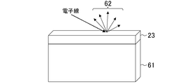
- FIG. 4 The outline of the measuring method by EBSP method is shown in FIG.
- a first coat film 23 made of AlN is formed on the front end face of a so-called laser bar 61 in which the wafer having the laser structure formed thereon is subjected to primary cleavage so that the resonator end face is exposed.
- the film thickness of the first coat film 23 is 20 nm.
- the electron beam incident for measurement is scattered by the lattice plane of the crystal, and the scattered electron beams interfere with each other and are strongly detected as a diffraction line 62.
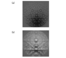
- FIGS. 5A and 5B show EBSP diffraction images of the first coat (AlN) film 23 showing different alignment axes.
- FIG. 5 (a) corresponds to c-axis oriented AlN
- FIG. 5 (b) shows measurement results corresponding to m-axis oriented AlN.
- the electron beam is accelerated and irradiated to about 10 keV to 30 keV, and the convergence of the electron beam is about 20 nm to 50 nm.
- the focused electron beam is scanned within a desired area to obtain a two-dimensional crystal orientation map.
- a diffraction image of the scattered electron beam (diffracted ray 62) is taken by a CCD camera.
- the scanning range of the electron beam is 1 ⁇ m ⁇ 1 ⁇ m, and the scanning interval of the electron beam is 10 nm. Further, the acceleration energy of the electron beam is 20 keV. In FIG. 4, the incident angle of the incident electron beam is measured at an inclination of 70 ° with respect to the sample laser bar 61.
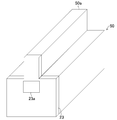
- FIG. 6 schematically shows a state in which the first coat film 23 is formed in the semiconductor laser device according to the first embodiment.
- the measurement region of EBSP according to the present embodiment is the light emission region 23 a on the lower side of the ridge waveguide 50 a in the first coat film 23.
- the area in which the end face deterioration and the optical destruction of the end face occur is limited to the light emitting area 23a and the peripheral portion. Therefore, the evaluation of the crystal orientation of the first coat film 23 may be performed centering on the light emission area 23a. However, if it is only the evaluation of the crystal orientation of the first coat film 23, it is not necessary to limit to the light emitting area 23a, and it may be anywhere on the end face of the semiconductor laminate 50.
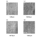
- FIGS. 7A to 7D show two-dimensional EBSP maps of the first coat film 23 made of AlN formed under four different film forming conditions.
- domain boundaries in which the tilt angle or rotation angle of the crystal orientation plane differs by 2 ° or more are indicated by solid lines.
- the measurement area is a square area of 1 ⁇ m on a side, and the respective domain boundary lengths are shown below each map.
- argon (Ar) is used as a reference gas in all cases, and the flow rate of Ar gas is 20 ml / min (standard state).
- the flow rate of nitrogen (N 2 ) gas as the reactive gas is 3.5 ml / min (standard state) in FIG. 7A, and 5.5 ml / min (FIG. 7B). In FIG. 7 (c), it is 10 ml / min (standard state), and in FIG. 7 (d), it is 15 ml / min (standard state).
- ml / min (standard state) is a unit representing the flow rate of a gas
- 1 ml / min (standard state) is a gas (standard state gas) converted at 0 ° C. and 1 atm for a certain gas. It represents a flow of 1 ml per minute.
- the grain size of the AlN film formed under the film forming condition with the highest partial pressure of nitrogen shown in FIG. 7D is extremely small, and the domain boundary length is 138.6 ⁇ m ⁇ 1 . It shows a large value.
- the domain boundary length tends to increase. That is, it is understood that the grain size tends to decrease as the nitrogen flow rate increases.
- FIG. 8 shows the relationship between the flow rate of nitrogen and the boundary length of the domain when the flow rate of Ar gas is 20 ml / min (standard state). As described above, the domain boundary length increases as the nitrogen flow rate increases.
- the applicant examined various film forming conditions under which the domain boundary length is further reduced.
- the flow rate of Ar gas is set to 30 ml / min (standard state), and the flow rate of nitrogen gas is 5.2 ml (standard). It has been found that, in the state (1), it is possible to obtain an AlN film having a domain boundary length of 1 ⁇ m ⁇ 1 or less and having a very high single crystallinity.
- FIG. 9 is a two-dimensional EBSP map of an AlN film obtained when the flow rate of Ar gas is 30 ml / min (standard state) and the flow rate of nitrogen gas is 5.2 ml (standard state).
- the domain boundary length is as very small as 75 nm, and it can be seen that the film has extremely high single crystallinity.
- the conditions for obtaining such an AlN film having high single crystallinity are not limited to the above.
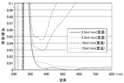
- FIG. 10 is an extinction coefficient spectrum obtained from the transmission spectrum of the AlN film.
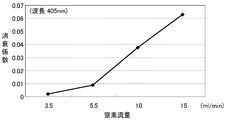
- FIG. 11 shows the relationship between the extinction coefficient and the nitrogen flow rate for light with a wavelength of 405 nm used in Blu-ray (registered trademark).
- the extinction coefficient increases as the flow rate of nitrogen increases. Further, as shown in FIG. 11, it can be seen that the extinction coefficient for light with a wavelength of 405 nm also increases as the nitrogen flow rate increases. That is, when FIG. 8 is compared with FIGS. 10 and 11, it is understood that the extinction coefficient tends to increase as the value of the domain boundary length increases.
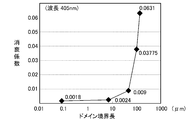
- FIG. 12 shows the relationship between the domain boundary length and the extinction coefficient for light with a wavelength of 405 nm. It can be seen that the extinction coefficient increases rapidly when the domain boundary length is greater than 7 ⁇ m ⁇ 1 . That is, it can be seen that the longer the grain boundary length and hence the more micro domains, the greater the light absorption.
- the origin of light absorption in the visible light region of the AlN film is an intermediate level derived from a defect inside a crystal, a grain boundary, and an interface between domains.
- a large number of defects and dangling bonds are present at grain boundaries and at the interface between domains, which are considered to be the main factor of light absorption in the visible light region. For this reason, as shown in FIG. 12, it is considered that the light absorption tends to increase as the value of the domain boundary length increases.
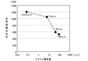
- FIG. 13 shows the relationship between the optical breakdown light output (COD) level and the domain boundary length after operating at a temperature of 70 ° C. for 600 hours in a constant operation reliability test with a light output of 160 mW.
- COD optical breakdown light output
- the domain boundary length of the AlN film required as the end face protective film needs to be 46 ⁇ m ⁇ 1 or less.
- the domain boundary length is 7 [mu] m -1 or less.
- the domain boundary length is an average index of the domain size in the AlN film, the actual facet destruction occurs in the light transmission region from which light is emitted. Therefore, if there is a domain boundary in the light transmission region, light absorption will occur.
- the high reliability can be maintained when the domain boundary length is 7 ⁇ m ⁇ 1 or less because the density of the interface between the domains decreases and the number of domain interfaces present in the laser light transmission region decreases.
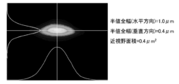
- the area of the light transmission region in the first coat film of the semiconductor laser device according to the first embodiment is about 0.4 ⁇ m 2 .
- the laser beam has a full width half maximum in the horizontal direction of about 1.0 ⁇ m and a full width half maximum in the vertical direction of 0.4 ⁇ m. Therefore, in a unit area of 1 ⁇ m 2 , 2.5 rectangles each having a long side of 1.0 ⁇ m and a short side of 0.4 ⁇ m are contained.
- the maximum value of the domain boundary length at this time is 5.0 ⁇ m ⁇ 1 . In order for the domain size to be larger than the beam size of laser light, the domain boundary length must be 5 ⁇ m ⁇ 1 or less.
- the domain size is 7 ⁇ m -1 or less, but in a high-power laser device, the domain size is larger, ie, AlN having high single crystallinity. A membrane is required.
- the domain size may be larger than the beam size of laser light, and in the nitride semiconductor laser device according to the present embodiment, the domain boundary length is preferably 5.0 ⁇ m ⁇ 1 . In other words, an AlN film with a domain size larger than 0.4 ⁇ m 2 is desirable.
- the domain boundary length of the AlN film according to the first embodiment is 75 nm as shown in FIG. 9, and as shown in FIG. 12, its extinction coefficient is as transparent as 0.002 or less, and its single crystal property is high. It is a membrane. As a result, as shown in FIG. 13, the optical breakdown light output after operating for 600 hours at a continuous operation light output of 160 mW maintains a very high level of 1200 mW.
- a GaN-based semiconductor laser device is generally manufactured by epitaxial growth on a hexagonal crystal growth substrate in which the main surface is a c-plane of plane orientation.
- the plane orientation of the cleavage plane is m-plane.
- Aluminum nitride has the most stable hexagonal crystal structure and has the highest growth rate by c-axis growth, so c-axis growth can be performed on an underlayer in the amorphous state or on a substrate made of silicon (Si).
- Si silicon
- the underlayer is hexagonal and m-plane
- the present inventors have found that it is possible to grow m-axis by increasing ion energy at the time of film formation.
- the crystal orientation axis is c axis or m axis. Therefore, in the second embodiment, an example of forming a c-axis grown or m-axis grown AlN film having a small value of the domain boundary length will be described.
- the reliability of the nitride semiconductor laser device is related to the domain boundary length of the crystal forming the protective film.
- the extinction coefficient also increases as the value of the domain boundary length increases, regardless of whether the orientation of the protective film (the first coat film 23) is the m axis or the c axis, and the optical breakdown light output is It decreases with the operation time.
- the stress given to the semiconductor stack 50 tends to be smaller in the m-axis orientation than in the c-axis orientation.
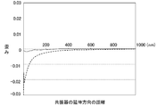
- FIG. 15 shows the effect of strain in the m-axis direction on the GaN crystal when the m-axis oriented AlN film and the c-axis oriented AlN film are formed respectively on the m-plane of the GaN crystal by ECR sputtering. It represents.
- a graph shown by a solid line represents an AlN film with m axis orientation
- a graph shown by a broken line represents an AlN film with c axis orientation.
- the flow rate of Ar gas at the time of forming an m-axis oriented AlN film is 8 ml / min (standard state), and the flow rate of N 2 gas is 5.5 ml / min (standard state).
- This condition is an example of the film formation condition of the m-axis oriented AlN film found by the inventor of the present invention, and the film formation condition of the m-axis oriented AlN film is not limited to this.
- the flow rate of Ar gas at the time of forming the c-axis oriented AlN film is 20 ml / min (standard state), and the flow rate of N 2 gas is 5.5 ml / min (standard state).
- a first AlN film having a thin film thickness with m-axis orientation is formed as a lower film, and then an upper film is formed on the first AlN film.
- a second AlN film with c-axis alignment may be formed to form an AlN film (first coat film) composed of two layers.
- the c-axis is spontaneously oriented if it does not depend on the substrate.
- a certain amount of energy is required to follow the crystal structure of the base, as in epitaxial growth. Therefore, in the case of the ECR sputtering method, a method of increasing the ion energy of Ar ions for assisting the film formation of the AlN film is effective. In order to increase the ion energy of Ar ions, it is sufficient to increase the RF power and microwave power for generating plasma.
- the RF power and the microwave output are formed as 500 W to obtain the c-axis oriented AlN film. Therefore, by setting the RF power to 600 W, an m-axis oriented AlN film can be obtained.
- the film is formed at a flow rate of Ar gas of 20 ml / min (standard state) or 30 ml / min (standard state). Therefore, in the second embodiment, the pressure of the entire chamber is reduced by reducing the flow rate of Ar gas to 8 to 10 ml / min (standard state), thereby generating Ar ions with higher ion energy. The assistance of this Ar ion makes it possible to obtain an m-axis oriented AlN film.
- the orientation of the AlN film can be controlled by the film forming conditions, and an AlN film having higher single crystallinity can be obtained, so that a nitride semiconductor laser device having high reliability can be realized.
- the present invention relates to a light emitting diode device using a group III nitride semiconductor It is also effective in improving the reliability of Also in the light emitting diode element, oxidation of the nitride semiconductor at the light emitting end face of the element and external diffusion of nitrogen occur during operation, so current leakage at the light emitting end face increases, leading to a decrease in light emission efficiency.
- the present invention is not limited to a group III nitride semiconductor, and is effective for a semiconductor light emitting device using GaAs or InP. Also in these semiconductor light emitting devices, the oxidation of the semiconductor at the light emitting end face during operation and the external diffusion of semiconductor constituent atoms are the cause of the end face deterioration.
- the nitride semiconductor light emitting device has an end face protective film which has little light absorption even at the time of high power operation and does not cause optical destruction, and has a long life and high reliability.
- n-type substrate 12 n-type GaN layer 13 n-type cladding layer 14 n-type light guide layer 15 multiple quantum well active layer 16 p-type light guide layer 17 p-type electron block layer 18 p-type superlattice cladding layer 19 p-type contact layer 20 mask layer 21 P side electrode 22 N side electrode 23 first coat film 23 a light emitting area 24 second coat film 25 multilayer coat film 50 semiconductor laminated body 51 semiconductor laser device 50 a ridge waveguide 52 stem 52 a electrode terminal 52 b laser holding portion 53 Cap 53a Window 54 Glass Plate 55 Gas 61 Laser Bar 62 Diffraction Line
Abstract
窒化物半導体装置は、III族窒化物半導体からなり、発光端面を有する半導体積層体(50)と、該半導体積層体(50)における発光端面を覆うように形成された第1コート膜(23)とを有している。第1コート膜(23)は、アルミニウムを含む窒化物からなる結晶性膜である。該結晶性膜は、結晶配向面における傾斜角度と回転角度とが互いに同一である複数のドメインの集合体からなり、単位面積当たりの各ドメインの境界の長さは、7μm-1以下である。
Description
本発明は、窒化物半導体発光装置に関し、特に発光端面に保護膜を設けた窒化物半導体発光装置に関する。
半導体発光装置のうち、半導体レーザ装置は、コンパクトディスク(CD)、デジタル汎用ディスク(DVD)及びブルーレイディスク(Blu-ray Disc)(登録商標)等に代表される光ディスクメディアの再生及び記録用の光源として広く使用されている。特に、高速度の情報記録動作が求められており、短時間で多くの情報を記録するために半導体レーザ装置の高出力化が必要不可欠となっている。
しかしながら、一般に、半導体レーザ装置は、光出力が増大すると、動作電流が徐々に増加する劣化現象や、光学破壊と呼ばれる現象により半導体レーザ装置が発振しなくなる現象が知られている。従って、高出力化を実現するために、このような半導体レーザ装置の劣化を抑制又は防止する研究開発が活発になされている。特に光学破壊を伴う頓死は、レーザ共振器の光出射面であるフロント端面で生じるため、共振器端面を覆う保護膜の堅牢化及び安定化等の取り組みが行われている。一般に、半導体レーザ装置の共振器端面は保護膜により覆われており、該共振器端面における反射率の制御、異物の付着防止及び共振器端面の酸化防止を果たしている。
図16に、特許文献1に記載された従来の窒化物半導体レーザ装置の模式的な断面構成を示す。図16に示すように、従来の窒化物半導体レーザ装置は、活性層(発光層)102と、該活性層102を挟むn型半導体層101及びp型半導体層103とからなるレーザ構造体100を有している。p型半導体層103にはp側電極104が形成され、n型半導体層101にはn側電極105が形成されている。
レーザ構造体100における共振器のミラーとして機能するリア端面には、酸化ケイ素(SiO2)又は酸化アルミニウム(Al2O3)等の金属酸化物からなる保護膜106が設けられている。また、共振器のフロント端面には、第1の保護膜107として窒化アルミニウム(AlN)が用いられ、第1の保護膜107の外側には第2の保護膜108として酸化アルミニウム(Al2O3)が用いられている。
ここで、高出力化における半導体レーザ装置の劣化原因の1つは、レーザ構造体100の発熱と光吸収とによって生じる第1の保護膜107等と半導体の端面との固相反応や、各保護膜中の残留酸素又はパッケージ中の酸素がレーザ発振に伴って保護膜中を拡散して共振器端面を酸化する等の、共振器端面の界面反応が原因であると考えられている。
また、レーザ発振時の発熱によって、レーザ構造体100から各保護膜が剥がれたり、レーザ構造体100にクラック等が生じたりして物理的な破壊が生じる。図16に示す従来の第1の保護膜107であるAlNは結晶性薄膜であるため、堅牢であり熱伝導性も良く、端面コート膜として非常に優れた材料である。その上、AlNは窒化物半導体と同様に窒化物であるため、レーザ構造体100との固相反応も抑制される。
しかしながら、AlN膜は膜応力が大きく、レーザ発振動作によってクラックの発生等が生じやすい。また、AlNには波長が400nmの近辺に欠陥等に起因する光吸収帯が存在することが知られており、レーザ発振時の光吸収により、発熱及び酸素の拡散を引き起こすと考えられている。
そこで、特許文献2には、膜応力を小さくするAlN膜の構成と成膜方法とが記載されている。特許文献2においては、互いに異なる結晶配向性を持つAlN膜を積層することによって膜応力を緩和し、発熱によるクラック及び膜剥がれを抑制している。
また、特許文献3には、酸素の拡散を抑制するために、希土類元素を添加したAlNを保護膜として用いる構成が記載されている。希土類をAlNに添加することにより、希土類元素が酸素と結合して、酸素の拡散を抑制することが可能となる。このような希土類元素を添加したAlN膜を用いることにより、通常のAlN膜を用いる場合と比べて共振器端面の酸化及び膜剥がれを防ぎ、光学破壊や端面の劣化を抑制して、長時間のレーザ動作が可能となる。
しかしながら、特許文献2に記載されたAlN膜は、膜剥がれやクラックの発生を抑制できるものの、端面の発熱や光吸収によって生じる端面の酸化等による光学破壊が発生するという問題がある。特許文献2においては、互いに結晶配向性が異なるAlN膜を積層しているため、異なる結晶配向性を持つAlN膜同士の間に界面が生じ、光吸収の起源となる。その上、特許文献1のAlN膜は多結晶質であり、グレイン同士の界面において光吸収が生じる。このようなAlN膜による光吸収は、共振器端面の発熱及びAlN膜中の酸素の拡散を引き起こして光学破壊につながるため、半導体レーザ装置の信頼性を低下させる原因となる。
また、特許文献3に開示されている、イットリウム(Y)等の希土類元素を添加したAlN膜においても、共振器端面の劣化や光学破壊が生じるという問題がある。これは、Yの添加によってAlN膜のグレインが微小化してグレイン界面の面積が増大することにより、AlN膜の光吸収が増大するためと考えられる。このように、AlN膜は結晶性膜であることから、熱及び光による劣化は小さいものの、光吸収による発熱及び酸素の拡散が共振器端面の劣化を引き起こすことから、半導体レーザ装置の寿命及びその信頼性を低下させる原因となる。
本発明は、前記の問題を解決し、高出力動作時においても光吸収が少なく、光学破壊を起こさない端面保護膜を得られるようにすることを目的とする。
前記の目的を達成するため、本発明は、窒化物半導体発光装置を、端面保護膜にアルミニウムを含む窒化物からなる結晶性膜を用い、該結晶性膜を所定の大きさで且つ結晶配向面における傾斜角度と回転角度とが互いに同一であるドメインの集合体により形成する構成とする。なお、ドメインの定義は後述する。
具体的に、本発明に係る第1の窒化物半導体発光装置は、III族窒化物半導体からなり、発光端面を有する半導体積層体と、半導体積層体における発光端面を覆うように形成された第1の保護膜とを備え、第1の保護膜は、アルミニウムを含む窒化物からなる結晶性膜であり、結晶性膜は、結晶配向面における傾斜角度と回転角度とが互いに同一である複数のドメインの集合体からなり、単位面積当たりの各ドメインの境界の長さは、7μm-1以下である。
第1の窒化物半導体発光装置によると、アルミニウムを含む窒化物からなる結晶性を有する第1の保護膜は、単位面積当たりの各ドメインの境界の長さが7μm-1以下であることから、すなわち単一ドメインの面積が大きい。これにより、単位面積当たりのドメイン同士の間の界面の面積が小さくなって、光吸収が小さくなるので、動作中の発熱及び酸素の拡散を抑制することができる。その結果、高出力で且つ長寿命の窒化物半導体発光装置を実現できる。
本発明に係る第2の窒化物半導体発光装置は、III族窒化物半導体からなり、発光端面を有する半導体積層体と、半導体積層体における発光端面を覆うように形成された第1の保護膜とを備え、第1の保護膜は、アルミニウムを含む窒化物からなる結晶性膜であり、結晶性膜は、結晶配向面における傾斜角度と回転角度とが互いに同一である複数のドメインの集合体からなり、複数のドメインのうち発光端面の光透過領域と対向するドメインの面積は光透過領域の面積よりも大きい。
第2の窒化物半導体発光装置によると、アルミニウムを含む窒化物からなる結晶性を有する第1の保護膜は、結晶配向面における傾斜角度と回転角度とが互いに同一である複数のドメインの集合体からなり、複数のドメインのうち発光端面の光透過領域と対向するドメインの面積は光透過領域の面積よりも大きい。これにより、発光端面から出射される発光光がドメイン同士の界面によって光吸収又は散乱されることがない。従って、動作中の発熱、酸素の拡散及び散乱による光損失をより確実に抑制できるため、高出力で且つ長寿命の窒化物半導体発光装置を実現できる。
第1又は第2の窒化物半導体発光装置において、第1の保護膜は、結晶配向面における傾斜角度及び回転角度が共に2°以内である単一のドメインを有していることが好ましい。
このようにすると、第1の保護膜における単一のドメインが大きくなって、界面の面積が小さくすることができる。
第1又は第2の窒化物半導体発光装置において、第1の保護膜は、半導体積層体の結晶軸配向と同一の結晶軸配向を持つ結晶構造を有していてもよい。
このようにすると、第1の保護膜が半導体積層体に与える膜応力を低減することができるため、第1の保護膜の膜剥がれ及びクラックの発生を防止することが可能となる。
また、第1又は第2の窒化物半導体発光装置において、第1の保護膜は、半導体積層体の結晶軸配向と異なる結晶軸配向を持つ結晶構造を有していてもよい。
このようにすると、第1の保護膜の光吸収係数をより小さくすることができる。
第1又は第2の窒化物半導体発光装置において、半導体積層体の結晶構造は六方晶であり、発光端面はm面であり、第1の保護膜はc軸配向していてもよい。
このようにすると、第1の保護膜による光吸収係数が小さくなる。
第1又は第2の窒化物半導体発光装置は、第1の保護膜を覆うように形成された第2の保護膜をさらに備え、第2の保護膜は、酸素を含む非晶質膜であってもよい。
このようにすると、非晶質の第2の保護膜によって、発光端面の応力が緩和されるため、第1の保護膜の膜剥がれ及びクラックの発生を抑制できる。
本発明に係る窒化物半導体発光装置は、高出力動作時においても光吸収が少なく、光学破壊を起こさない端面保護膜を得られるため、長寿命で且つ高信頼性を実現することができる。
(第1の実施形態)
本発明の第1の実施形態について図面を参照しながら説明する。
本発明の第1の実施形態について図面を参照しながら説明する。
第1の実施形態に係る窒化物半導体発光装置を、窒化ガリウム(GaN)系青紫色レーザ装置として、その製造方法と共に説明する。
まず、図1(a)に示すように、例えば有機金属気相堆積(MOCVD)法により、n型GaNからなるn型基板11の上に、複数のIII族窒化物半導体からなる半導体積層体50をエピタキシャル成長する。
具体的には、面方位のc面(=(0001)面)を主面とするn型基板11の主面上に、厚さが約1μmでn型ドーパントであるSiの濃度が1×1018cm-3のn型GaN層12、厚さが約1.5μmでSiの濃度が5×1017cm-3のn型Al0.05Ga0.95Nからなるn型クラッド層13、厚さが約0.1μmでSiの濃度が5×1017cm-3のn型GaNからなるn型光ガイド層14、InGaNからなる多重量子井戸活性層15、厚さが約0.1μmでp型ドーパントであるMgの濃度が1×1019cm-3のp型GaNからなるp型光ガイド層16、厚さが約10nmでMgの濃度が1×1019cm-3のp型Al0.2Ga0.8Nからなるp型電子ブロック層17、p型AlGaNからなるp型超格子クラッド層18及び厚さが約20nmでMgの濃度が1×1020cm-3のp型GaNからなるp型コンタクト層19を順次成長する。
ここで、多重量子井戸活性層15は、厚さが約3nmのアンドープのInGaNからなる井戸層と、厚さが7nmのアンドープのIn0.02Ga0.98Nからなる障壁層とにより構成された三重量子井戸構造を有する。井戸層のIn組成は、発振波長が405nmとなるように調整されている。また、p型超格子クラッド層18は、それぞれMgの濃度が1×1019cm-3で且つ厚さが約2nmの、p型Al0.1Ga0.9Nとp型GaNとからなる超格子構造を有し、合計の膜厚は0.5μmである。
次に、図1(b)に示すように、p型コンタクト層19の上に、SiO2からなるマスク層20を形成する。続いて、リソグラフィ法及びエッチング法により、マスク層20をn型基板11の結晶軸に対して<1-100>方向に延びるストライプ状にパターニングする。続いて、ストライプ状にパターニングされたマスク層20を用いて、p型コンタクト層19及びp型超格子クラッド層18に対してドライエッチングを行うことにより、p型コンタクト層19及びp型超格子クラッド層18に、結晶軸の<1-100>方向に延びるストライプ状のリッジ導波路50aを形成する。ここで、p型超格子クラッド層18におけるリッジ導波路50aの側方部分の厚さ(残し膜厚)は約0.1μmとしている。また、リッジ導波路50aの下部の幅は約2μmとし、リッジ導波路50aの上部の幅は約1.4μmとしている。
次に、図2に示すように、マスク層20を除去し、その後、リソグラフィ法及び真空蒸着法等により、リッジ導波路50aを構成するp型コンタクト層19の上に、パラジウム(Pd)からなるP側電極21を形成する。続いて、n型基板11をへき開が容易となるように薄膜化(裏面研磨)する。その後、n型基板11の裏面に、チタン(Ti)からなるN側電極22を形成する。
続いて、半導体積層体50におけるリッジ導波路50aの下方に形成される共振器の長さが約600μm又は約800μmとなるように、n型基板11及び半導体積層体50をへき開する。このへき開により、半導体積層体50には、面方位が(1-100)面からなる端面ミラーが形成される。なお、本願明細書において、結晶軸及び面方位の指数に付した負の符号”-”は該符号に続く一の指数の反転を便宜的に表している。その後、共振器の各端面には、半導体積層体50の端面の劣化を防止すると共に端面の反射率を調整するためのコート膜をそれぞれ形成する。
具体的には、図2に示すように、レーザ光が出射するフロント端面には、第1の保護膜として窒化アルミニウム(AlN)からなる第1コート膜23を形成し、該第1コート膜23の上には、第2の保護膜として酸化アルミニウム(Al2O3)からなり、非晶質の第2コート膜24を形成する。また、フロント端面と対向するリア端面には、酸化アルミニウム(Al2O3)/酸化ジルコニウム(ZrO2)とを複数対で積層した多層コート膜25を形成する。但し、リア端面は、所望の反射率を得られる構成であれば、AlON/SiO2、Al2O3/SiO2又はAlN/Al2O3を複数対で積層した構成としてもよい。ここで、リア端面においても、特にリア端面と接する第1の保護膜にはフロント端面と同様に、AlN膜を用いることが望ましい。AlN膜は堅牢で熱伝導性にも優れており、光出射がないリア端面においても、保護膜として適している。本実施形態においては、フロント端面の反射率を約10%とし、リア端面の反射率は約90%としている。なお、フロント端面及びリア端面の各コート膜の膜厚は、所望の反射率を得られるように適宜設計される。
第1の実施形態に係るAlNからなる第1コート膜23は、電子サイクロトロン共鳴(ECR)スパッタ法を用いて形成している。ECRスパッタ法の他に、高周波(RF)スパッタ法又はマグネトロンスパッタ法を用いることができる。
ECRスパッタ法は、スパッタイオンが半導体積層体50のへき開端面に直接に照射されないため、イオン照射が引き起こす半導体表面の結晶欠陥の密度を低減できる。このため、半導体レーザ装置における端面コートの成膜法として適している。なお、第1コート膜23を構成するAlNは、スパッタのターゲット材として、AlNからなるターゲット材と窒素(N2)ガスとの組み合わせ、又はAlからなるターゲット材と窒素ガスとの組み合わせによる反応性スパッタにより成膜が可能である。本実施形態においては、金属精錬により純度を容易に高めることができるAlからなる金属ターゲット材に、基準ガスとしてアルゴン(Ar)と、反応性ガスとして窒素ガスとを組み合わせて用いている。
第1コート膜23の膜厚は、約6nmに設定している。AlN膜は膜応力が大きいことから、AlN膜を半導体積層体50のへき開端面に50nm以上の厚膜で成膜すると膜剥がれが生じる。また、光吸収による発熱を抑えるには、第1コート膜23中の光の光路長を短くすることが望ましく、このことからも第1コート膜23の膜厚は50nm以下でなければならない。一方、AlN膜を3nm以下の薄膜として形成した場合には、AlN膜を酸素等が透過しやすくなるため、半導体積層体50の端面が酸化される要因となる。また、薄膜はプロセスの制御が困難であり、膜厚にばらつきが生じてしまう。以上から、AlNからなる第1コート膜23の膜厚は3nm以上且つ50nm以下が望ましい。
図3に各コート膜23、24、25を形成した後の、パッケージされた状態の半導体レーザ装置51を示す。図3に示すように、半導体レーザ装置51は、例えば、一の面に複数の電極端子52aが形成され、他の面にレーザ保持部52bが形成された金属からなるステム52のレーザ保持部52bの上に固着されている。ステム52には、半導体レーザ装置51及びレーザ保持部52bを覆うと共に、該半導体レーザ装置51のフロント端面と対向する位置に窓部53aを有する金属からなるキャップ53が固着されている。該窓部53aには、内側からガラス板54が固着されて、ステム52とキャップ53とから構成される空間は密閉される。密閉されたキャップ53の内部は、水分を含まない乾燥空気又はアルゴン等の希ガスからなる気体55が充填されている。
上述したように、第1の実施形態に係るAlNからなる第1コート膜23は、Alからなる金属ターゲット材を用いたECRスパッタ法により成膜されており、その成膜条件における各ガスの流量は、それぞれ室温で、アルゴン(Ar)ガスを30ml/minとし、窒素(N2)ガスを5.2ml/minとしている。この成膜条件で得られる第1コート膜23は、同一配向で構成されるドメインのサイズが相対的に大きくなるため、物質の光吸収の指数である消衰係数(光吸収係数)が小さい。従って、レーザ動作中の光吸収による発熱、酸素の拡散及び端面の酸化が抑制され、その結果、共振器端面の劣化を防ぐことができる。
以下、第1コート膜23を構成するAlN膜の結晶ドメインについて詳細に述べる。ここで、ドメインとは、同一の結晶構造及び同一の配向(結晶軸配向)を有し、その配向面及び配向角が同一であるグレインの集合体と定義する。本願発明者らは、ECRスパッタの成膜条件によってAlNのドメインサイズが大きく影響を受けることを突き止めている。本実施形態に係る成膜条件は、ドメインサイズが大きいAlN膜を得られるものの、ドメインサイズが大きいAlN膜の成膜条件はこれに限られず、本実施形態は一例である。
本願発明者らは、端面保護膜におけるドメインサイズと光学破壊出力との関係に相関があることを見出した。ここで、ドメインサイズの指標となるパラメータとして、ドメイン境界長を定義する。ドメイン境界長とは、単位面積当たりに存在するドメイン界面の総距離を表すパラメータである。ここで、単一ドメインとは、同一配向を有する結晶体において、配向面の傾斜角度及び回転角度が同一である連続した領域であると定義する。配向面の傾斜角度及び回転角度のうち、いずれか一方でも同一でなければ異なるドメインとし、従って、境界が存在することになる。このドメイン同士の間の境界の単位面積(μm-2)当たりの総距離(μm)がドメイン境界長に相当する。ドメイン境界長の値が大きいということは、ドメイン面積が小さいことを意味しており、言い換えると薄膜が多結晶であり、配向のばらつきが大きいということになる。一方、ドメイン境界長の値が小さいということは、ドメインサイズが大きいことを意味しており、単結晶性が高い薄膜であるといえる。ここで、単一ドメインは、単一グレインとは完全に同義ではない。しかし、ドメイン境界長の値が大きいということはそれだけ多くのドメインが存在することから、成膜における結晶の不均一性が大きいことに相当する。すなわち、ドメイン境界長が長いということは、ドメインサイズが小さく、グレインサイズも小さいことを意味している。
ここで、ドメインが同一でないことの条件、すなわちドメイン境界を区別するための境界条件が必要となる。本実施形態においては、配向面の回転角度及び傾斜角度が2°以内の場合を同一配向ドメインと定義している。ドメイン境界を区別するための境界条件の設定角度が小さければ小さいほど、単一ドメインと単一グレインとは等しくなる。しかしながら、設定角度が小さ過ぎると、実際には連続な単結晶膜であったとしても、少しの歪みやラフネス等によって、異なるドメインと評価されてしまうため、測定誤差の原因となる。従って、設定角度は、ドメインの結晶配向を測定する手法の測定誤差よりも大きくなるような条件が望ましい。逆に、設定角度が大き過ぎると、類似するドメインの区別ができず、ドメイン境界長の指標の正確性が損なわれる。よって、設定角度は、配向性の測定における空間分解能及びばらつきに応じた値とする必要がある。
なお、第1の実施形態においては、ドメイン境界を区別する設定角度を2°としたが、上述した通りこれには限られず、0.5°以上且つ5°未満程度であればよい。
以下に、本実施形態に係る第1コート膜23を構成するAlN膜におけるドメイン境界長の測定方法の詳細を説明する。AlN膜における結晶配向性は、後方電子線散乱回折法(Electron Back Scattering Diffraction Pattern:EBSD又はEBSP)によって測定できる。EBSP法とは、電子線ビームを試料表面に収束して照射し、試料表面により散乱される回折電子線像を撮像することにより、試料(薄膜)の結晶配向性を評価する手法である。
図4にEBSP法による測定方法の概略を示す。図4に示すように、レーザ構造が形成されたウェハを共振器端面が露出するように1次へき開した状態の、いわゆるレーザバー61のフロント端面に、AlNからなる第1コート膜23が成膜されている。ここでは、第1コート膜23の膜厚を20nmとしている。測定用に入射された電子線は結晶の格子面で散乱され、散乱された電子線が互いに干渉して回折線62として強く検出される。
図5(a)及び図5(b)に、互いに異なる配向軸を示す第1コート(AlN)膜23のEBSP回折像を示す。図5(a)はc軸配向したAlNと対応しており、図5(b)はm軸配向したAlNと対応する測定結果をそれぞれ表している。このように、同一の結晶構造であっても配向性の相違から回折パターンが異なるため、結晶の配向性を評価することができる。ここで、電子線は10keV~30keV程度に加速して照射しており、電子線の収束は20nm~50nm程度である。この収束された電子線を所望の面積内で走査して、2次元の結晶配向マップを得る。散乱電子線(回折線62)の回折像はCCDカメラによって撮像される。
本実施形態に係るEBSP測定法では、電子線の走査範囲を1μm×1μmとし、電子線の走査間隔を10nmとしている。また、電子線の加速エネルギーは20keVとしている。図4において、入射電子線の入射角度は、試料であるレーザバー61に対して70°傾斜させて測定している。
図6に第1の実施形態に係る半導体レーザ装置に、第1のコート膜23を成膜した状態を模式的に示す。本実施形態に係るEBSPの測定領域は、第1のコート膜23におけるリッジ導波路50aの下側の光出射領域23aである。第1のコート膜23と接触する半導体積層体50において、端面劣化及び端面の光学破壊が起こる領域は光出射領域23aとその周辺部分に限られている。このため、第1のコート膜23の結晶配向性の評価についても、光出射領域23aを中心に行えばよい。但し、第1のコート膜23の結晶配向性の評価のみであれば、光出射領域23aに限る必要はなく、半導体積層体50の端面上であればどこでも構わない。
図7(a)~図7(d)に、4通りの異なる成膜条件で成膜したAlNからなる第1コート膜23の2次元EBSPマップを示す。ここでは、結晶配向面の傾斜角度又は回転角度が2°以上異なるドメイン境界を実線で示している。前述したように、測定領域は1辺が1μmの正方形領域であり、各マップの下にはそれぞれのドメイン境界長を示している。
ECRスパッタの成膜条件として、基準ガスにはいずれもアルゴン(Ar)を用いており、Arガスの流量は20ml/min(標準状態)としている。一方、反応性ガスとしての窒素(N2)ガスの流量は、図7(a)においては、3.5ml/min(標準状態)とし、図7(b)においては、5.5ml/min(標準状態)とし、図7(c)においては、10ml/min(標準状態)とし、図7(d)においては、15ml/min(標準状態)としている。なお、ここでml/min(標準状態)とは、気体の流量を表す単位であり、1ml/min(標準状態)は、ある気体について0℃、1気圧の気体(標準状態の気体)換算で1分間当たり1ml流れることを表す。
図7(a)に示す2次元EBSPマップは、窒素の分圧が最も低い成膜条件であり、単位面積(1μm2)当たりのドメイン境界長は6.99μm/μm2(=μm-1)と小さい値であるのに対して、図7(d)に示す窒素の分圧が最も高い成膜条件で成膜したAlN膜はグレインが極めて小さく、そのドメイン境界長は138.6μm-1と大きな値を示す。このように、窒素の流量が増加するのに伴ってドメイン境界長が増大する傾向がある。すなわち、窒素流量の増加に伴って、グレインサイズが小さくなる傾向があることが分かる。
図8にArガスの流量を20ml/min(標準状態)とした場合の窒素の流量とドメイン境界長との関係を示す。上述したように、窒素流量の増加に伴ってドメイン境界長が増大している。
本願出願人は、ドメイン境界長がより一層小さくなるような成膜条件を種々検討し、その結果、Arガスの流量を30ml/min(標準状態)とし、窒素ガスの流量を5.2ml(標準状態)とすれば、ドメイン境界長が1μm-1以下の、非常に単結晶性が高いAlN膜を得られることを見出した。
図9はArガスの流量を30ml/min(標準状態)とし、窒素ガスの流量を5.2ml(標準状態)とした場合に得られたAlN膜の2次元EBSPマップである。この場合のドメイン境界長は75nmと非常に小さく、極めて単結晶性が高い膜であることが分かる。しかしながら、このような単結晶性が高いAlN膜を得られる条件は上記に限られない。
次に、図7(a)~図7(d)に示したAlN膜の消衰係数(光吸収係数)を調べた結果を示す。図10は、AlN膜の透過分光スペクトルから得られた消衰係数スペクトルである。また、図11はブルーレイ(登録商標)で用いられる波長が405nmの光における消衰係数と窒素流量との関係を示している。
図10に示すように、窒素の流量が増加するに従って消衰係数が増大することが分かる。また、図11に示すように、波長が405nmの光における消衰係数も窒素流量が増加するに従って大きくなることが分かる。すなわち、図8と、図10及び図11とを比較すると、ドメイン境界長の値が大きくなると消衰係数も大きくなる傾向があることが分かる。
図12にドメイン境界長と波長が405nmの光における消衰係数との関係を示す。ドメイン境界長が7μm-1よりも大きくなると、消衰係数が急激に増大することが分かる。すなわち、グレイン境界長が長く、従って微小ドメインが多くなるほど、光吸収が大きくなることが分かる。一般に、AlN膜の可視光領域における光吸収の起源は、結晶内部の欠陥、粒界及びドメイン同士の界面由来の中間準位であると考えられている。特に粒界及びドメイン同士の界面には、多数の欠陥及びダングリングボンドが存在し、可視光領域における光吸収の主要因になっていると考えられている。このため、図12に示すように、ドメイン境界長の値が大きくなると、光吸収が大きくなる傾向が現れると考えられる。
次に、ドメイン境界長と半導体レーザ装置の信頼性との関係について説明する。
図13は光出力が160mWで一定の連続動作信頼性試験において、70℃の温度下で600時間動作させた後の光学破壊光出力(COD)レベルとドメイン境界長との関係を表している。図13からは、ドメイン境界長が短くなるのに従って光学破壊光出力の値が大きくなり、高い信頼性を示すことが分かる。このようにドメイン境界長が短く、すなわちドメインサイズが大きいほど信頼性が高くなることが分かる。特にドメイン境界長が46μm-1から7μm-1の領域にかけて、光学破壊光出力の値が急激に上昇しているのが分かる。
上述したように、ドメイン境界長が長くなるとドメインサイズが小さくなり、光吸収が増大する。これはドメイン境界に存在する欠陥又はダングリングボンドに由来する中間準位の影響であると考えられる。一方、電極から注入されたキャリアもこのような中間準位が存在すると、非発光再結合が増加して発光効率が減少する。中間準位による光吸収も中間準位を介した非発光再結合も共に発熱を伴った過程であることから、共振器端面の温度上昇につながって端面破壊を引き起こすと考えられる。
従って、図12に示す関係から、ドメイン境界長が46μm-1以下であれば、消衰係数は0.01以下と非常に小さくなる。すなわち、端面保護膜として求められるAlN膜のドメイン境界長は46μm-1以下である必要がある。
さらに、図13に示す関係から、光学破壊光出力はドメイン境界長が7μm-1以下であれば高いレベルが維持されるため、ドメイン境界長は7μm-1以下が望ましい。ドメイン境界長はAlN膜におけるドメインサイズの平均的な指標ではあるものの、実際の端面破壊は光が出射する光透過領域において起こる。このため、光透過領域にドメイン境界が存在すれば光吸収が起こることになる。ドメイン境界長が7μm-1以下で高い信頼性を維持できるのは、ドメイン同士の界面の密度が減少してレーザ光の透過領域に存在するドメイン界面が少なくなるためであると考えられる。
ここで、図14に示すように、第1の実施形態に係る半導体レーザ装置の第1のコート膜における光の透過領域の面積を測定すると0.4μm2程度である。面積が1μm2の単位面積に0.4μm2のドメインが2.5個存在する場合、そのドメイン境界長はどのような値になるかを以下に計算する。
図14から、レーザ光は水平方向の半値全幅が1.0μm程度であり、垂直方向の半値全幅が0.4μmである。従って、面積が1μm2の単位面積中に長辺が1.0μmで、短辺が0.4μmの長方形が2.5個入ることになる。このときのドメイン境界長の最大値は5.0μm-1となる。ドメインサイズがレーザ光のビームサイズよりも大きくなるためには、ドメイン境界長が5μm-1以下でなければならない。先述のように、ドメインサイズは7μm-1以下であれば、高い信頼性を持つレーザ装置を得られるが、さらに高出力なレーザ装置においては、ドメインサイズはさらに大きい、すなわち単結晶性が高いAlN膜が求められる。このとき、ドメインサイズはレーザ光のビームサイズよりも大きくなればよく、本実施形態に係る窒化物半導体レーザ装置においては、ドメイン境界長は5.0μm-1が望ましい。言い換えると、ドメインサイズは0.4μm2よりも大きいAlN膜が望ましい。
なお、第1の実施形態に係るAlN膜のドメイン境界長は、図9に示すように75nmであり、図12に示すようにその消衰係数も0.002以下と透明で単結晶性が高い膜である。これにより、図13に示すように、連続動作光出力が160mWで600時間動作させた後の光学破壊光出力は1200mWと非常に高いレベルを維持している。
(第2の実施形態)
以下、本発明の第2の実施形態について図面を参照しながら説明する。
以下、本発明の第2の実施形態について図面を参照しながら説明する。
GaN系半導体レーザ装置は、一般に、主面が面方位のc面である六方晶の結晶成長用基板にエピタキシャル成長して作製される。この場合、レーザ構造の共振器端面はへき開によって形成されるため、そのへき開面の面方位はm面となる。
m面を持つ共振器端面の上にAlN膜を成膜する場合は、成膜条件によって共振器端面の結晶構造と同一配向であるm軸成長と、共振器端面の結晶構造とは異なる配向であるc軸成長とを選択することが可能である。
窒化アルミニウム(AlN)は六方晶が最安定構造であり、c軸成長による成長速度が最も大きいことから、アモルファス状態の下地層又はシリコン(Si)からなる基板上には、c軸成長することが知られている。しかしながら、本願発明者らは、下地層が六方晶であり且つm面の場合に、成膜時のイオンエネルギーを増大すると、m軸成長させることが可能であることを突き止めた。
AlNからなる保護膜において、結晶配向軸をc軸とするかm軸とするかは選択可能である。従って、第2の実施形態においては、ドメイン境界長の値が小さいc軸成長又はm軸成長したAlN膜の成膜例を説明する。
窒化物半導体レーザ装置における信頼性は、保護膜を構成する結晶のドメイン境界長と関係があることは第1の実施形態で説明した。このとき、保護膜(第1コート膜23)の配向性がm軸であるかc軸であるかに拘わらず、ドメイン境界長の値が大きいほど消衰係数も大きくなり、光学破壊光出力は動作時間と共に小さくなる。しかしながら、m軸配向の方がc軸配向の場合と比べて半導体積層体50に与えるストレスが小さくなる傾向があることを、以下に示す歪み解析の結果から得ている。
図15にEBSP法によりm軸配向のAlN膜とc軸配向のAlN膜とに対して行った歪み解析の解析結果を示す。図15は、GaN結晶のm面上にm軸配向したAlN膜とc軸配向したAlN膜とをECRスパッタ法によりそれぞれ成膜した場合の該GaN結晶に及ぼすm軸方向への歪みの影響を表している。ここで、実線で示すグラフがm軸配向のAlN膜を表し、破線で示すグラフがc軸配向のAlN膜を表している。ここで、m軸配向のAlN膜を成膜する際のArガスの流量は8ml/min(標準状態)であり、N2ガスの流量は5.5ml/min(標準状態)である。この条件は本願発明者が見出したm軸配向のAlN膜の成膜条件の一例であって、m軸配向のAlN膜の成膜条件はこれに限られない。また、c軸配向のAlN膜を成膜する際のArガスの流量は20ml/min(標準状態)であり、N2ガスの流量は5.5ml/min(標準状態)である。
図15からは、m軸配向したAlN膜の方がc軸配向したAlN膜よりも歪みが小さいことが分かる。これは、m軸配向したAlN膜には貫通転移が発生し、ストレスがc軸配向したAlN膜と比べて緩和しているためであると推測される。このことから、m軸配向したAlN膜の方がc軸配向したAlN膜よりもGaN結晶に与える応力の影響が小さいといえる。しかしながら、AlN膜に貫通転移が発生するとドメイン境界長の値が大きくなるため、端面保護膜としてはc軸配向したAlN膜が適している。
その上、貫通転移は膜厚が大きくなると発生しやすくなるため、下層膜としてm軸配向で膜厚が薄い第1のAlN膜を成膜し、次いで第1のAlN膜の上に上層膜としてc軸配向した第2のAlN膜を成膜して、2層からなるAlN膜(第1のコート膜)を形成してもよい。
次に、m軸配向又はc軸配向のAlN膜の成膜方法について説明する。
前述したように、AlN膜はc軸方向の成長速度が速いため、下地に依存しない場合は自発的にc軸配向する。m面を主面とする基板上にAlN膜を成長させる場合は、エピタキシャル成長のように下地の結晶構造を踏襲するため、一定のエネルギーが必要となる。そこで、ECRスパッタ法の場合、AlN膜の成膜をアシストするArイオンのイオンエネルギーを増大する方法が有効である。Arイオンのイオンエネルギーを増大するには、プラズマを発生させるためのRFパワー及びマイクロ波の出力を増大させればよい。
第1の実施形態においては、RFパワー及びマイクロ波出力を500Wとして成膜し、c軸配向のAlN膜を得ている。そこで、RFパワーを600Wに設定することにより、m軸配向のAlN膜を得ることがきる。
また、m軸配向のAlN膜を得るには、成膜中のチャンバ内の圧力を下げることも有効である。本願発明者らは、上記のように、イオンの加速エネルギーが大きい方がAlN膜のm軸成長を促すことを明らかにした。例えば、第1の実施形態においては、Arガスの流量を20ml/min(標準状態)又は30ml/min(標準状態)で成膜している。そこで、第2の実施形態においては、Arガスの流量を8~10ml/min(標準状態)に流量を下げることによりチャンバ内全体の圧力を低下し、よりイオンエネルギーが大きいArイオンを生成する。このArイオンのアシストにより、m軸配向したAlN膜を得ることができる。
このように、成膜条件によってAlN膜の配向性を制御することが可能となり、より単結晶性が高いAlN膜を得られることから、高い信頼性を有する窒化物半導体レーザ装置を実現できる。
なお、第1及び第2の各実施形態においては、III族窒化物、すなわちGaN系半導体を用いた半導体レーザ装置を用いて説明したが、本発明はIII族窒化物半導体を用いた発光ダイオード素子の信頼性の向上にも有効である。発光ダイオード素子においても、素子の発光端面での窒化物半導体の酸化と窒素の外部拡散が動作中に生じるため、発光端面での電流リークが増大して、発光効率の低下を招くからである。
また、本願発明は、III族窒化物半導体に限られず、GaAs又はInPを用いた半導体発光装置に対しても有効である。これらの半導体発光装置においても、動作中における発光端面での半導体の酸化及び半導体構成原子の外部拡散が端面劣化の要因であるからである。
本発明に係る窒化物半導体発光装置は、高出力動作時においても光吸収が少なく、光学破壊を起こさない端面保護膜を有しており、長寿命で且つ高信頼性の窒化物半導体発光装置等に有用である。
11 n型基板
12 n型GaN層
13 n型クラッド層
14 n型光ガイド層
15 多重量子井戸活性層
16 p型光ガイド層
17 p型電子ブロック層
18 p型超格子クラッド層
19 p型コンタクト層
20 マスク層
21 P側電極
22 N側電極
23 第1コート膜
23a 光出射領域
24 第2コート膜
25 多層コート膜
50 半導体積層体
51 半導体レーザ装置
50a リッジ導波路
52 ステム
52a 電極端子
52b レーザ保持部
53 キャップ
53a 窓部
54 ガラス板
55 気体
61 レーザバー
62 回折線
12 n型GaN層
13 n型クラッド層
14 n型光ガイド層
15 多重量子井戸活性層
16 p型光ガイド層
17 p型電子ブロック層
18 p型超格子クラッド層
19 p型コンタクト層
20 マスク層
21 P側電極
22 N側電極
23 第1コート膜
23a 光出射領域
24 第2コート膜
25 多層コート膜
50 半導体積層体
51 半導体レーザ装置
50a リッジ導波路
52 ステム
52a 電極端子
52b レーザ保持部
53 キャップ
53a 窓部
54 ガラス板
55 気体
61 レーザバー
62 回折線
Claims (7)
- III族窒化物半導体からなり、発光端面を有する半導体積層体と、
前記半導体積層体における前記発光端面を覆うように形成された第1の保護膜とを備え、
前記第1の保護膜は、アルミニウムを含む窒化物からなる結晶性膜であり、
前記結晶性膜は、結晶配向面における傾斜角度と回転角度とが互いに同一である複数のドメインの集合体からなり、
単位面積当たりの前記各ドメインの境界の長さは、7μm-1以下である窒化物半導体発光装置。 - III族窒化物半導体からなり、発光端面を有する半導体積層体と、
前記半導体積層体における前記発光端面を覆うように形成された第1の保護膜とを備え、
前記第1の保護膜は、アルミニウムを含む窒化物からなる結晶性膜であり、
前記結晶性膜は、結晶配向面における傾斜角度と回転角度とが互いに同一である複数のドメインの集合体からなり、
前記複数のドメインのうち前記発光端面の光透過領域と対向するドメインの面積は、前記光透過領域の面積よりも大きい窒化物半導体発光装置。 - 請求項1又は2において、
前記第1の保護膜は、前記結晶配向面における傾斜角度及び回転角度が共に2°以内である単一のドメインを有している窒化物半導体発光装置。 - 請求項1又は2において、
前記第1の保護膜は、前記半導体積層体の結晶軸配向と同一の結晶軸配向を持つ結晶構造を有している窒化物半導体発光装置。 - 請求項1~3のいずれか1項において、
前記第1の保護膜は、前記半導体積層体の結晶軸配向と異なる結晶軸配向を持つ結晶構造を有している窒化物半導体発光装置。 - 請求項1~3及び5のいずれか1項において、
前記半導体積層体の結晶構造は六方晶であり、
前記発光端面はm面であり、
前記第1の保護膜はc軸配向している窒化物半導体発光装置。 - 請求項1~6のいずれか1項において、
前記第1の保護膜を覆うように形成された第2の保護膜をさらに備え、
前記第2の保護膜は、酸素を含む非晶質膜である窒化物半導体発光装置。
Priority Applications (2)
| Application Number | Priority Date | Filing Date | Title |
|---|---|---|---|
| CN201080021734.8A CN102484354B (zh) | 2009-05-20 | 2010-01-19 | 氮化物半导体发光装置 |
| US13/294,682 US8437376B2 (en) | 2009-05-20 | 2011-11-11 | Nitride semiconductor light-emitting device |
Applications Claiming Priority (2)
| Application Number | Priority Date | Filing Date | Title |
|---|---|---|---|
| JP2009122287A JP5383313B2 (ja) | 2009-05-20 | 2009-05-20 | 窒化物半導体発光装置 |
| JP2009-122287 | 2009-05-20 |
Related Child Applications (1)
| Application Number | Title | Priority Date | Filing Date |
|---|---|---|---|
| US13/294,682 Continuation US8437376B2 (en) | 2009-05-20 | 2011-11-11 | Nitride semiconductor light-emitting device |
Publications (1)
| Publication Number | Publication Date |
|---|---|
| WO2010134229A1 true WO2010134229A1 (ja) | 2010-11-25 |
Family
ID=43125923
Family Applications (1)
| Application Number | Title | Priority Date | Filing Date |
|---|---|---|---|
| PCT/JP2010/000262 WO2010134229A1 (ja) | 2009-05-20 | 2010-01-19 | 窒化物半導体発光装置 |
Country Status (4)
| Country | Link |
|---|---|
| US (1) | US8437376B2 (ja) |
| JP (1) | JP5383313B2 (ja) |
| CN (1) | CN102484354B (ja) |
| WO (1) | WO2010134229A1 (ja) |
Cited By (2)
| Publication number | Priority date | Publication date | Assignee | Title |
|---|---|---|---|---|
| WO2014002339A1 (ja) * | 2012-06-29 | 2014-01-03 | パナソニック株式会社 | 窒化物半導体発光素子 |
| WO2019159449A1 (ja) * | 2018-02-14 | 2019-08-22 | パナソニックIpマネジメント株式会社 | 窒化物半導体レーザ素子及び照明光源モジュール |
Families Citing this family (15)
| Publication number | Priority date | Publication date | Assignee | Title |
|---|---|---|---|---|
| JP6085150B2 (ja) * | 2012-03-16 | 2017-02-22 | 株式会社日立ハイテクサイエンス | 試料作製装置及び試料作製方法 |
| DE102012102306B4 (de) * | 2012-03-19 | 2021-05-12 | OSRAM Opto Semiconductors Gesellschaft mit beschränkter Haftung | Laserdiodenvorrichtung |
| DE102012102305A1 (de) * | 2012-03-19 | 2013-09-19 | Osram Opto Semiconductors Gmbh | Laserdiodenvorrichtung |
| US8867582B2 (en) | 2012-04-04 | 2014-10-21 | Osram Opto Semiconductors Gmbh | Laser diode assembly |
| US8737445B2 (en) * | 2012-04-04 | 2014-05-27 | Osram Opto Semiconductors Gmbh | Laser diode assembly |
| US9008138B2 (en) | 2012-04-12 | 2015-04-14 | Osram Opto Semiconductors Gmbh | Laser diode device |
| DE102012103160A1 (de) | 2012-04-12 | 2013-10-17 | Osram Opto Semiconductors Gmbh | Laserdiodenvorrichtung |
| WO2014002959A1 (ja) * | 2012-06-25 | 2014-01-03 | 三菱化学株式会社 | m面窒化物系発光ダイオードの製造方法 |
| WO2014097508A1 (ja) * | 2012-12-19 | 2014-06-26 | パナソニック株式会社 | 窒化物半導体レーザ素子 |
| JP6387190B2 (ja) * | 2015-07-15 | 2018-09-05 | 住友電気工業株式会社 | 被膜 |
| JP2017143139A (ja) * | 2016-02-09 | 2017-08-17 | 株式会社東芝 | 半導体装置およびその製造方法 |
| KR20190099394A (ko) | 2016-12-28 | 2019-08-27 | 스미토모덴키고교가부시키가이샤 | 피막 |
| DE102017112610A1 (de) | 2017-06-08 | 2018-12-13 | Osram Opto Semiconductors Gmbh | Kantenemittierender Halbleiterlaser und Betriebsverfahren für einen solchen Halbleiterlaser |
| GB2584150B (en) * | 2019-05-24 | 2021-05-19 | Plessey Semiconductors Ltd | LED precursor including a passivation layer |
| JP7438476B2 (ja) | 2019-08-20 | 2024-02-27 | 日亜化学工業株式会社 | 半導体レーザ装置及びその製造方法 |
Citations (3)
| Publication number | Priority date | Publication date | Assignee | Title |
|---|---|---|---|---|
| WO2003036771A1 (fr) * | 2001-10-26 | 2003-05-01 | Ammono Sp.Zo.O. | Laser a semi-conducteurs a base de nitrure et procede de production de ce laser |
| JP2006203162A (ja) * | 2004-12-20 | 2006-08-03 | Sharp Corp | 窒化物半導体発光素子およびその製造方法 |
| JP2009016798A (ja) * | 2007-06-07 | 2009-01-22 | Nichia Corp | 窒化物半導体レーザ素子 |
Family Cites Families (10)
| Publication number | Priority date | Publication date | Assignee | Title |
|---|---|---|---|---|
| JPH02288287A (ja) * | 1989-04-27 | 1990-11-28 | Sharp Corp | 半導体レーザ素子 |
| KR100904501B1 (ko) | 2001-10-26 | 2009-06-25 | 암모노 에스피. 제트오. 오. | 에피택시용 기판 |
| KR20050054482A (ko) | 2002-06-26 | 2005-06-10 | 암모노 에스피. 제트오. 오. | 질화물 반도체 레이저 디바이스 및 그의 성능을향상시키기 위한 방법 |
| CN1805230B (zh) * | 2004-12-20 | 2011-06-01 | 夏普株式会社 | 氮化物半导体发光元件及其制造方法 |
| JP2007201373A (ja) | 2006-01-30 | 2007-08-09 | Sharp Corp | 半導体レーザ素子 |
| JP4444304B2 (ja) | 2006-04-24 | 2010-03-31 | シャープ株式会社 | 窒化物半導体発光素子および窒化物半導体発光素子の製造方法 |
| JP5042609B2 (ja) | 2006-12-08 | 2012-10-03 | シャープ株式会社 | 窒化物系半導体素子 |
| US7646798B2 (en) * | 2006-12-28 | 2010-01-12 | Nichia Corporation | Nitride semiconductor laser element |
| JP4978454B2 (ja) | 2006-12-28 | 2012-07-18 | 日亜化学工業株式会社 | 窒化物半導体レーザ素子 |
| US7804872B2 (en) | 2007-06-07 | 2010-09-28 | Nichia Corporation | Nitride semiconductor laser element |
-
2009
- 2009-05-20 JP JP2009122287A patent/JP5383313B2/ja active Active
-
2010
- 2010-01-19 WO PCT/JP2010/000262 patent/WO2010134229A1/ja active Application Filing
- 2010-01-19 CN CN201080021734.8A patent/CN102484354B/zh active Active
-
2011
- 2011-11-11 US US13/294,682 patent/US8437376B2/en active Active
Patent Citations (3)
| Publication number | Priority date | Publication date | Assignee | Title |
|---|---|---|---|---|
| WO2003036771A1 (fr) * | 2001-10-26 | 2003-05-01 | Ammono Sp.Zo.O. | Laser a semi-conducteurs a base de nitrure et procede de production de ce laser |
| JP2006203162A (ja) * | 2004-12-20 | 2006-08-03 | Sharp Corp | 窒化物半導体発光素子およびその製造方法 |
| JP2009016798A (ja) * | 2007-06-07 | 2009-01-22 | Nichia Corp | 窒化物半導体レーザ素子 |
Cited By (4)
| Publication number | Priority date | Publication date | Assignee | Title |
|---|---|---|---|---|
| WO2014002339A1 (ja) * | 2012-06-29 | 2014-01-03 | パナソニック株式会社 | 窒化物半導体発光素子 |
| JP5491679B1 (ja) * | 2012-06-29 | 2014-05-14 | パナソニック株式会社 | 窒化物半導体発光素子 |
| US9202988B2 (en) | 2012-06-29 | 2015-12-01 | Panasonic Intellectual Property Management Co., Ltd. | Nitride semiconductor light-emitting element |
| WO2019159449A1 (ja) * | 2018-02-14 | 2019-08-22 | パナソニックIpマネジメント株式会社 | 窒化物半導体レーザ素子及び照明光源モジュール |
Also Published As
| Publication number | Publication date |
|---|---|
| CN102484354A (zh) | 2012-05-30 |
| US8437376B2 (en) | 2013-05-07 |
| JP2010272641A (ja) | 2010-12-02 |
| US20120057612A1 (en) | 2012-03-08 |
| JP5383313B2 (ja) | 2014-01-08 |
| CN102484354B (zh) | 2014-08-27 |
Similar Documents
| Publication | Publication Date | Title |
|---|---|---|
| JP5383313B2 (ja) | 窒化物半導体発光装置 | |
| US7773648B2 (en) | Semiconductor device and method for manufacturing the same | |
| US7602829B2 (en) | Semiconductor light emitting device and method of manufacturing same | |
| US9202988B2 (en) | Nitride semiconductor light-emitting element | |
| US8319235B2 (en) | Nitride semiconductor light-emitting device and method of manufacturing nitride semiconductor light-emitting device | |
| US7759684B2 (en) | Nitride semiconductor light emitting device and method for fabricating the same | |
| US8571083B2 (en) | Nitride semiconductor laser chip | |
| US20130070801A1 (en) | Semiconductor laser device and method of manufacturing the same | |
| US9312659B2 (en) | Nitride semiconductor laser element | |
| JP2011009374A (ja) | 窒化物半導体レーザ | |
| JP2005322944A (ja) | 窒化ガリウム系半導体発光素子の評価方法および製造方法 | |
| JP5670009B2 (ja) | 窒化物半導体レーザ素子 | |
| US20100133582A1 (en) | Nitride semiconductor light emitting device | |
| JP2008300802A (ja) | 半導体レーザ素子およびその製造方法 | |
| US7633983B2 (en) | Semiconductor laser device | |
| JP5572919B2 (ja) | 窒化物半導体レーザ素子 | |
| JP2002124702A (ja) | 窒化ガリウム系半導体発光素子 | |
| JP4066317B2 (ja) | 半導体レーザ素子、その製造方法及び光ディスク装置 | |
| JP2007013207A (ja) | 半導体発光素子 | |
| JP5681338B2 (ja) | 窒化物半導体レーザ素子 | |
| JP2011119540A (ja) | 窒化物半導体レーザ素子 | |
| JP2009267108A (ja) | 半導体発光素子及びそれを用いた半導体発光装置 | |
| JP5803167B2 (ja) | 窒化物半導体レーザ素子の製造方法 | |
| JP5488775B1 (ja) | 窒化物半導体レーザ素子 | |
| JP2007329487A (ja) | レーザ素子および光記録再生装置 |
Legal Events
| Date | Code | Title | Description |
|---|---|---|---|
| WWE | Wipo information: entry into national phase |
Ref document number: 201080021734.8 Country of ref document: CN |
|
| 121 | Ep: the epo has been informed by wipo that ep was designated in this application |
Ref document number: 10777469 Country of ref document: EP Kind code of ref document: A1 |
|
| NENP | Non-entry into the national phase |
Ref country code: DE |
|
| 122 | Ep: pct application non-entry in european phase |
Ref document number: 10777469 Country of ref document: EP Kind code of ref document: A1 |