WO2010116906A1 - 通信アドレス検出装置、制御回路内蔵コネクタ、及び、通信アドレス検出方法 - Google Patents
通信アドレス検出装置、制御回路内蔵コネクタ、及び、通信アドレス検出方法 Download PDFInfo
- Publication number
- WO2010116906A1 WO2010116906A1 PCT/JP2010/055437 JP2010055437W WO2010116906A1 WO 2010116906 A1 WO2010116906 A1 WO 2010116906A1 JP 2010055437 W JP2010055437 W JP 2010055437W WO 2010116906 A1 WO2010116906 A1 WO 2010116906A1
- Authority
- WO
- WIPO (PCT)
- Prior art keywords
- communication address
- combination
- voltage levels
- assigned
- voltage
- Prior art date
- Legal status (The legal status is an assumption and is not a legal conclusion. Google has not performed a legal analysis and makes no representation as to the accuracy of the status listed.)
- Ceased
Links
Images






Classifications
-
- H—ELECTRICITY
- H04—ELECTRIC COMMUNICATION TECHNIQUE
- H04L—TRANSMISSION OF DIGITAL INFORMATION, e.g. TELEGRAPHIC COMMUNICATION
- H04L12/00—Data switching networks
- H04L12/28—Data switching networks characterised by path configuration, e.g. LAN [Local Area Networks] or WAN [Wide Area Networks]
- H04L12/40—Bus networks
- H04L12/40006—Architecture of a communication node
- H04L12/40019—Details regarding a bus master
-
- G—PHYSICS
- G06—COMPUTING OR CALCULATING; COUNTING
- G06F—ELECTRIC DIGITAL DATA PROCESSING
- G06F3/00—Input arrangements for transferring data to be processed into a form capable of being handled by the computer; Output arrangements for transferring data from processing unit to output unit, e.g. interface arrangements
-
- H—ELECTRICITY
- H04—ELECTRIC COMMUNICATION TECHNIQUE
- H04L—TRANSMISSION OF DIGITAL INFORMATION, e.g. TELEGRAPHIC COMMUNICATION
- H04L61/00—Network arrangements, protocols or services for addressing or naming
- H04L61/50—Address allocation
- H04L61/5038—Address allocation for local use, e.g. in LAN or USB networks, or in a controller area network [CAN]
-
- H—ELECTRICITY
- H04—ELECTRIC COMMUNICATION TECHNIQUE
- H04L—TRANSMISSION OF DIGITAL INFORMATION, e.g. TELEGRAPHIC COMMUNICATION
- H04L61/00—Network arrangements, protocols or services for addressing or naming
- H04L61/50—Address allocation
- H04L61/5046—Resolving address allocation conflicts; Testing of addresses
-
- H—ELECTRICITY
- H04—ELECTRIC COMMUNICATION TECHNIQUE
- H04L—TRANSMISSION OF DIGITAL INFORMATION, e.g. TELEGRAPHIC COMMUNICATION
- H04L12/00—Data switching networks
- H04L12/28—Data switching networks characterised by path configuration, e.g. LAN [Local Area Networks] or WAN [Wide Area Networks]
- H04L12/40—Bus networks
- H04L2012/40267—Bus for use in transportation systems
- H04L2012/40273—Bus for use in transportation systems the transportation system being a vehicle
Definitions
- the present invention relates to a communication address detection device for detecting a communication address based on a combination of high or low voltage levels input to a plurality of communication address setting terminals, and a connector with a built-in control circuit including the communication address detection device And a communication address detection method used in the communication address detection apparatus.
- Vehicles such as automobiles are provided with a plurality of actuators for driving windows and mirrors.
- the plurality of actuators are connected to an electronic control unit (ECU) by a wire harness configured by bundling a plurality of electric wires.
- ECU electronice control unit
- Each actuator performs an operation according to the control information, such as opening / closing of a window and adjustment of a mirror angle, by transmitting / receiving control information via the wire harness.
- each communication address setting terminal As a general configuration for setting a communication address for each actuator described above, a plurality of communication address setting terminals are provided, and a communication address is set based on a combination of voltage levels input to the plurality of communication address setting terminals. What to do is known.
- the voltage level input to each communication address setting terminal is a power supply voltage or a high level close thereto (hereinafter also referred to as [1]), or a low level close to 0 V (hereinafter also referred to as [0]). is there.
- Such a plurality of communication address setting terminals are connected to a power supply voltage via a resistor (that is, pulled up), and a high level is inputted as a voltage level. Then, by connecting a predetermined communication address setting terminal among the plurality of communication address setting terminals to the ground via a jumper switch, a wire harness, or the like, a low level is input as a voltage level. In this way, by inputting a predetermined voltage level ([1] or [0]) combination to a plurality of communication address setting terminals, the communication address assigned to this voltage level combination is set in the actuator. Is done.
- a high level that is, a voltage level at the time of disconnection
- a low level that is, a voltage level at the time of a short circuit
- a malfunction such as a short circuit of a wire harness. That is, the voltage level to be input to the communication address setting terminal may be inverted due to the above-described problems.
- the combination of the voltage levels input to the communication address setting terminal of the actuator in which the above problem has occurred becomes the same as the combination of the voltage levels input to the communication address setting terminals of the other actuators, so that a plurality of actuators There was a risk of overlapping communication addresses.
- a communication address is assigned to each of a combination of a plurality of voltage levels input to the three communication address setting terminals a, b, and c.
- the same combination of levels results in overlapping communication addresses.
- the present invention aims to solve the problems related to the above problems. That is, the present invention has a communication address detection device and a control circuit built-in that can prevent abnormal operation even when the voltage level to be input to any one of a plurality of communication address setting terminals is reversed due to a malfunction. It is an object to provide a connector and a communication address detection method.
- a voltage level consisting of a high level or a low level input to a plurality of communication address setting terminals 21 as shown in the basic configuration diagram of FIG.
- a communication address detecting device that detects a communication address based on a combination, a relationship between the combination of the voltage levels and the communication address assigned thereto is predetermined, and the voltage level assigned to the communication address is determined.
- Communication address information that is determined to be a combination of the voltage levels to which the communication address is not assigned when any one of the voltage level combinations is inverted is stored.
- Communication address information storage means 172 and a plurality of communication address setting terminals Based on the communication address information stored in the communication address information storage unit 172, the voltage level detection unit 171a that detects the combination of the voltage levels input to 1, and the voltage level detection unit 171a detects the voltage level detection unit 171a.
- a communication address assignment determination unit 171b for determining whether or not the communication address is assigned to a combination of voltage levels, and a combination of the voltage levels detected by the voltage level detection unit 171a by the communication address assignment determination unit 171b.
- the communication address detecting device includes an abnormality processing unit 171c that performs a predetermined abnormality process when it is determined that the communication address is not assigned to the device.
- a second aspect of the present invention relates to the communication address detection apparatus according to the first aspect, wherein the combination of the voltage levels to which the communication address is assigned in the communication address information is included in the combination of the voltage levels. Selected from a plurality of combinations of the voltage levels where the number of levels is an even number, or selected from a plurality of combinations of the voltage levels where the number of high levels included in the combination of voltage levels is an odd number It is what is done.
- a communication address is detected based on a combination of a plurality of communication address setting terminals and a voltage level consisting of a high level or a low level input to the plurality of communication address setting terminals.
- a control circuit built-in connector comprising an address detecting device, wherein the communication address detecting device comprises the communication address detecting device of the first or second aspect.
- a communication address detection method used in a communication address detection apparatus for detecting a communication address based on a combination of high level or low level voltage levels input to a plurality of communication address setting terminals.
- the voltage level detection step for detecting the combination of the voltage levels input to the plurality of communication address setting terminals, and the relationship between the combination of the voltage levels and the communication address assigned thereto are determined in advance.
- the combination of the voltage levels to which the communication address is assigned is the combination of the voltage levels to which the communication address is not assigned when any one of the voltage level combinations is inverted.
- Communication address information that is defined to be The communication address assignment determination step for determining whether or not the communication address is assigned to the combination of the voltage levels detected in the voltage level detection step; and the communication address assignment determination step; An abnormality processing step of performing predetermined abnormality processing when it is determined that the communication address is not assigned to the combination of the voltage levels detected in the detection step.
- the combination of the voltage levels to which the communication address is assigned in the communication address information is inverted (that is, the high level is one of the voltage level combinations).
- the high level is one of the voltage level combinations.
- it is set to low level or low level to high level it is determined to be a combination of voltage levels to which no communication address is assigned, so a combination of voltage levels to which a communication address is assigned is input.
- one of the terminals is input to the plurality of communication address setting terminals when the input voltage level is reversed due to a failure such as disconnection or short circuit of the wire harness.
- the communication address is not assigned to a combination of voltage levels
- a combination of voltage levels that are input to a plurality of communication address setting terminals based on the communication address information without overlapping with a combination of voltage levels to which other communication addresses are assigned. Can be detected, and predetermined abnormality processing can be performed. Therefore, even when the voltage level to be input to any one of the plurality of communication address setting terminals is reversed due to a malfunction, abnormal operation can be prevented.
- a combination of voltage levels to which a communication address is assigned in communication address information is (a) a plurality of voltage levels at which the number of high levels included in the combination of voltage levels is “even”. Since it is selected from among a plurality of combinations of voltage levels where (b) the number of high levels included in the combination of voltage levels is “odd”, for example, in communication address information
- the combination of the voltage levels to which the communication addresses are assigned is the above (a)
- the combination of the voltage levels to which the communication address in the communication address information is assigned is the above (b)
- the level is inverted, the number of communication address setting terminals to which a high level is input becomes “even”. Therefore, it is possible to detect an abnormality in the combination of voltage levels by counting the number of communication address setting terminals to which a high level is input. For example, a voltage to which a communication address is assigned with reference to a data table or the like Compared to the configuration for detecting the combination of levels, the processing is simpler, and an abnormality occurring in the combination of voltage levels input to a plurality of communication address setting terminals can be detected quickly and easily.
- the communication address detection device of the first or second aspect since the communication address detection device of the first or second aspect is provided, the voltage level to be input to any one of the plurality of communication address setting terminals is defective. Even in the case of inversion, abnormal operation can be prevented.
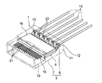
- FIG. 3 is a perspective view of the control circuit built-in connector of FIG. 2.
- FIG. 3 is a perspective view of a control circuit package provided in the control circuit built-in connector of FIG. 2.
- IC namely, Integrated Circuit
- IC namely, Integrated Circuit
- the control circuit built-in connector is, for example, an electronic device such as various actuators for opening and closing windows and adjusting the angle of a door mirror, and a control device such as an ECU for controlling the electronic devices over a network by data communication. Used to connect. For this reason, the control circuit built-in connector incorporates a circuit element for controlling data communication and the like.
- such a control circuit built-in connector (indicated by reference numeral 1 in the figure) is connected to an electronic device 70 such as an actuator one-on-one via an electric wire 15.
- a plurality of control circuit built-in connectors 1 (reference numerals 1A, 1B, 1C) connected to the electronic device 70 are connected to a plurality of harness-side connectors 51 provided on one wire harness 50, respectively.
- An electronic control unit (ECU) 60 is connected to one end of the wire harness 50, and the plurality of control circuit built-in connectors 1 and the ECU 60 are connected to each other by a bus.
- Each of the control circuit built-in connectors 1A, 1B, 1C is connected (fitted) to the harness side connector 51, so that different communication addresses are assigned to a plurality of communication address setting terminals A provided later.
- a combination of voltage levels consisting of a high level (ie, [1]) or a low level (ie, [0]) is input.
- communication addresses “0”, “1”, and “2” are set in the control circuit built-in connectors 1A, 1B, and 1C, respectively, and a communication address “3” is set in the ECU 60.
- Each control circuit built-in connector 1A, 1B, 1C receives, for example, various control information flowing on the wire harness 50, and determines whether or not to process the received control information based on the set communication address. . Then, if it is determined that it should be processed, the control information is transmitted to the electronic device 70. If it is determined that it should not be processed, the control information is discarded.
- the control circuit built-in connector 1 includes an outer housing 5 and a control circuit package 6 as shown in FIG.
- the outer housing 5 is formed in a flat box shape, and includes a unit housing 7 and a cover portion 8.
- the unit housing 7 is made of an insulating synthetic resin, and integrally includes a cylindrical hood portion 10 and a control circuit package housing chamber 11 connected to the hood portion 10.
- the hood portion 10 is fitted with the harness-side connector 51 when the connector housing of the harness-side connector 51 provided in the wire harness 50 enters.
- the control circuit package housing chamber 11 is formed in a U-shaped cross section, and an opening 12 is provided upward in FIG.
- the cover portion 8 is made of an insulating synthetic resin and is formed in a flat plate shape.
- the cover portion 8 is attached to the unit housing 7 so as to close the opening 12.
- the control circuit package 6 includes a lead frame 16, an IC chip 17 as a circuit element, and a resin sealing body 18.
- the lead frame 16 is made of a conductive metal, and integrally includes a chip holding portion 19, a plurality of press contact terminals 20, a plurality of male tabs 21, and a plurality of connecting portions 22.
- the control circuit package 6 is housed in the control circuit package housing chamber 11 of the unit housing 7.
- the chip holding part 19 is formed in a flat plate shape.
- the chip holding part 19 positions the IC chip 17 on its surface by bonding with epoxy, Ag paste, solder or the like.
- the press contact terminal 20 is integrally provided with a parallel portion 23 and a standing portion 24.
- the parallel portion 23 is formed in a band plate shape, and both surfaces thereof are provided on the same plane as both surfaces of the chip holding portion 19.
- the standing portion 24 is erected from one end of the parallel portion 23 of the press contact terminal 20 upward in FIG.
- the plurality of press contact terminals 20 are arranged such that their parallel portions 23 are parallel to each other and their standing portions 24 are erected in the same direction. Further, the other end of the parallel portion 23 of the plurality of press contact terminals 20 is directed to the chip holding portion 19 side.
- the standing portion 24 includes a pair of press contact blades 25 spaced apart from each other along the width direction of the press contact terminal 20, that is, the direction in which the plurality of press contact terminals 20 are arranged.
- the press contact blade 25 sandwiches the electric wire 15 between them and cuts a covering portion of the electric wire 15 to contact the core wire.
- both surfaces of the standing portion 24 are orthogonal to both surfaces of the parallel portion 23.
- the male tab 21 is formed in a rod shape extending linearly.
- the plurality of male tabs 21 are arranged in parallel at intervals.
- the plurality of male tabs 21 position the chip holding portions 19 between the plurality of press contact terminals 20.
- the male tab 21 is disposed in the hood portion 10 with the tip thereof facing the opening of the hood portion 10, and when the harness-side connector 51 is fitted to the hood portion 10, the terminal fitting ( (Not shown) and electrically connected.
- some of the plurality of male tabs 21 are assigned to the communication address setting terminal A (indicated by reference numerals 21a, 21b, and 21c), and the other part is assigned to the control information terminal B. The remainder is assigned to the power supply terminal C.
- the connecting portion 22 is formed to be bent from the press contact terminal 20 and the male tab 21 toward the chip holding portion 19. Some of the connecting portions 22 connect the chip holding portion 19 and the press contact terminal 20, and the other remaining connecting portions 22 connect the chip holding portion 19 and the male tab 21.
- the IC chip 17 is a circuit element that is disposed on the chip holding unit 19 and attached to the lead frame 16.
- the IC chip 17 is connected to each connecting portion 22 by a known bonding wire.
- the IC chip 17 electrically connects the press contact terminal 20 and the male tab 21 according to a predetermined pattern via the connecting portion 22. As described above, the IC chip 17 is mounted on the lead frame 16.
- the IC chip 17 is a well-known microcomputer, and as shown in FIG. 5, a central processing unit (CPU) 171, a ROM 172 that is a read-only memory, and a RAM that is a memory that can be read and rewritten (that is, a RAM). , Random Access Memory) 173, input port 174, and input / output port 175.
- the IC chip 17 corresponds to the communication address detection device in the claims.
- the CPU 171 manages various types of control in the control circuit built-in connector 1 and executes various types of processing including control according to the present invention in accordance with various control programs stored in the ROM 172.
- the ROM 172 stores various information such as communication address information J1 determined in advance with respect to the control program and the relationship between the combination of voltage levels input to the communication address setting terminals 21a, 21b, and 21c and the communication address assigned thereto. is doing. That is, the ROM 172 corresponds to communication address information storage means in the claims.
- the communication address information J1 includes a communication address table J11 indicating a relationship between a combination of voltage levels input to the communication address setting terminals 21a, 21b, and 21c and a communication address assigned thereto, and a communication address.
- high level number type information J12 indicating the type of high level number (even or odd) included in the combination of voltage levels to which the communication address is assigned in the table J11.
- the communication address table J11 only combinations of voltage levels to which communication addresses are assigned are set. In other words, a communication address is not assigned to a combination of voltage levels not included in the communication address table J11, and when such a combination of voltage levels is detected, it can be determined that an abnormality has occurred. it can.
- the combination of voltage levels included in the communication address table J11 is set so that the number of high levels included therein (that is, the number of [1]) is “even”. In the present embodiment, the number of high levels included in the combination of voltage levels is set to 2 for the communication addresses “0” to “2” and 0 for the communication address “3”, ie, an even number. ing.
- information indicating “even” is set in the high-level number type information J12.
- the voltage level of any one of the combinations of the voltage levels is inverted (that is, the high level is set to the low level or the low level is set to the high level)
- the voltage level to which no communication address is assigned is set. Change to a combination.
- the communication address setting terminals 21a, 21b, and 21c when a combination of voltage levels to which communication addresses are assigned is input to the communication address setting terminals 21a, 21b, and 21c, one low level to be input due to a failure such as disconnection of the wire harness. If the high level is erroneously input to the communication address setting terminal, the number of communication address setting terminals to which the high level is input becomes “odd”. In addition, if a low level is erroneously input to one communication address setting terminal to which a high level is to be input due to a failure such as a short circuit of a wire harness, the number of communication address setting terminals to which a high level is input is “Odd”.
- the present invention is not limited to this, and the number of high levels is set to “odd”. Also good.
- the ROM 172 stores a program for causing the CPU 171 to function as various means such as a voltage level detection means, a communication address assignment determination means, and an abnormality processing means.
- the CPU 171 functions as the various means described above by executing the program.
- the RAM 173 appropriately stores data, programs, and the like necessary for the CPU 171 to execute various processes.
- the RAM 173 is provided with an area (communication address area) for setting a communication address detected based on a combination of voltage levels input to the communication address setting terminals 21a, 21b, and 21c.
- the CPU 171 uses the communication address stored in the communication address area to determine processing of various control information received from the ECU 60, generate various control information to be transmitted to the ECU 60, and the like.
- the input port 174 is a well-known general-purpose input port, and is connected to the communication address setting terminal A (that is, the terminals 21a, 21b, and 21c) of the male tab 21, and inputs the voltage level of these terminals to the CPU 171.
- the input part to which the terminals 21a, 21b, and 21c in the input port 174 are connected is connected to a power supply voltage (that is, pulled up) via a resistor (not shown) in the IC chip 17, and the power supply voltage or A high level close to that is input.
- the harness-side connector 51 When the harness-side connector 51 is fitted to the control circuit built-in connector 1, a predetermined terminal of the terminals 21a, 21b, and 21c is connected to the ground via the wire harness 50, and the voltage level is 0V or A near low level is input to the input section of the input port 174.
- the input / output port 175 is a well-known general-purpose input / output port and is connected to the control information terminal B of the male tab 21.
- the input / output port 175 inputs various control information sent from the ECU 60 via the wire harness 50 to the CPU 171 and outputs various control information generated by the CPU 171 to the ECU 60 via the wire harness 50.
- the power supply system wiring (that is, power supply and ground) of the IC chip 17 is connected to the power supply terminal C of the male tab 21.
- the resin sealing body 18 is made of a synthetic resin and is formed in a flat box shape.
- the resin sealing body 18 includes a chip holding portion 19, a parallel portion 23 of each press contact terminal 20, a base end portion of each male tab 21 near the chip holding portion 19, and each connecting portion 22 in the molding die. And sealed by molding. That is, the resin sealing body 18 seals the IC chip 17 and the lead frame 16 by protruding the press contact terminal 20 and the male tab 21.
- step S110 a combination of voltage levels input to the input port 174, that is, a combination of voltage levels input to the communication address setting terminals 21a, 21b, and 21c is detected. Then, the process proceeds to step S120.
- step S120 it is determined whether or not a communication address is assigned to the combination of voltage levels detected in step S110. Specifically, it is determined whether or not the combination of the voltage levels detected in step S110 is included in the communication address table J11 stored in the ROM 172. If included, the combination of the detected voltage levels is determined. It is determined that a communication address is assigned to the combination, and the process proceeds to step S130 (Y in S120). If not included, it is determined that a communication address is not assigned to the detected combination of voltage levels. Then, the process proceeds to step S140 (N in S120).
- the number of high levels included in the combination of voltage levels detected in step S110 may be used to determine whether a communication address is assigned to the combination of voltage levels. Specifically, the number of high levels included in the combination of voltage levels detected in step S110 is counted. When the type of the counted high level number (that is, even or odd) is the same as the information set in the high level number type information J12, a communication address is assigned to the combination of the detected voltage levels. When the type of the counted high level number is different from the information set in the high level number type information J12, a communication address is assigned to the detected voltage level combination. It may be determined that the error has not occurred (that is, an abnormality has occurred).
- the communication address can be determined using a data table or the like.
- the processing is simpler, and an abnormality occurring in the combination of the voltage levels input to the communication address setting terminals 21a, 21b, 21c can be detected quickly and easily. Can do.
- step S130 the communication address assigned to the combination of voltage levels detected in step S120 is acquired from the communication address table J11 stored in the ROM 172. Then, the acquired communication address is stored in a communication address area provided in the RAM 173. In this way, the communication address of the control circuit built-in connector 1 is detected (set). And the process of this flowchart is complete
- step S140 abnormality notification control information for notifying the ECU 60 that an abnormality has occurred in the combination of the voltage levels input to the communication address setting terminals 21a, 21b, and 21c is generated and input / output is performed. This is transmitted to the ECU 60 via the port 175, and all processes are stopped in order to prevent abnormal operations such as runaway (ie, predetermined abnormal processes). And the process of this flowchart is complete
- step S110 described above corresponds to the voltage level detection means in the claims
- step S120 corresponds to the communication address assignment determination means in the claims
- step S140 corresponds to the abnormality processing means in the claims. To do.
- step S110 described above corresponds to the voltage level detection step in the claims
- step S120 corresponds to the communication address assignment determination step in the claims
- step S140 corresponds to the abnormality processing step in the claims. To do.
- the control circuit built-in connector 1 is connected to the harness-side connector 51 of the wire harness 50.
- step S110 When the control circuit built-in connector 1 is powered on, a combination of voltage levels input to the communication address setting terminals 21a, 21b, and 21c is detected (step S110). Then, it is determined that the detected combination of voltage levels is a normal one to which a communication address is assigned (Y in step S120), and the assigned communication address is set (step S130).
- the control circuit built-in connector 1 when the control circuit built-in connector 1 is turned on, the combination of the voltage levels input to the communication address setting terminals 21a, 21b, and 21c is detected (step S110), and the detected voltage is detected. It is determined that the combination of levels is abnormal to which no communication address is assigned (N in step S120), and the occurrence of abnormality is notified to ECU 60 (step S140).
- the communication address setting terminals 21a, 21b, and 21c have a combination of voltage levels (terminals to which no communication address is assigned) (terminals).
- 21a, terminal 21b, terminal 21c) ([0], [0], [1]).
- the control circuit built-in connector 1 is turned on, the combination of the voltage levels input to the communication address setting terminals 21a, 21b, and 21c is detected (step S110), and the detected voltage is detected. It is determined that the combination of levels is abnormal to which no communication address is assigned (N in step S120), and the occurrence of abnormality is notified to ECU 60 (step S140).
- the combination of the voltage levels to which the communication address in the communication address table J11 of the communication address information J1 is assigned is inverted (that is, the high voltage level).
- the level is set to the low level or the low level is set to the high level, it is determined to be a combination of voltage levels to which no communication address is assigned.
- the plurality of communication address setting terminals 21a, 21b, and 21c to which one of them is input when one of the terminals is inverted due to a malfunction such as disconnection or short circuit of the wire harness 50, Input to communication address setting terminals 21a, 21b, 21c
- the combination of the voltage levels becomes a combination of the voltage levels to which no communication address is assigned.
- the combination of the voltage levels does not overlap with the combination of the voltage levels to which other communication addresses are assigned.
- An abnormality occurring in the combination of the voltage levels input to the communication address setting terminals 21a, 21b, and 21c can be detected, and a predetermined abnormality process can be performed. Therefore, even when the voltage level to be input to any one of the plurality of communication address setting terminals 21a, 21b, and 21c is inverted due to a malfunction, the abnormal operation can be prevented.
- a combination of voltage levels to which a communication address in the communication address table J11 of the communication address information J1 is assigned is selected from among a plurality of voltage level combinations in which the number of high levels included in the combination of voltage levels is “even”. Since it is selected, for example, when the voltage level of one of the plurality of communication address setting terminals 21a, 21b, and 21c is inverted due to disconnection or short circuit of the wire harness, the communication address setting in which a high level is input The number of terminals is “odd”. Therefore, it is possible to detect an abnormality in the combination of voltage levels by counting the number of communication address setting terminals to which a high level is input.
- a voltage to which a communication address is assigned with reference to a data table or the like Compared to the configuration for detecting the combination of levels, the processing is simpler, and an abnormality occurring in the combination of the voltage levels input to the plurality of communication address setting terminals 21a, 21b, and 21c can be detected quickly and easily.
- the number of high levels included in the combination of voltage levels to which communication addresses are assigned is “even”, but the present invention is not limited to this, and the number of high levels may be “odd”.
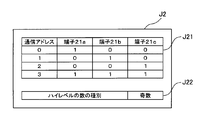
- FIG. 8 shows an example of information address information in which the number of high levels included in the combination of voltage levels to which communication addresses are assigned is “odd”.
- the communication address information J2 shown in FIG. 8 may be used instead of the communication address information J1 shown in FIG.
- the communication address information J2 includes a communication address table J21 indicating a relationship between a combination of voltage levels input to the communication address setting terminals 21a, 21b, and 21c and a communication address assigned to the combination.
- High-level number type information J12 indicating the type of high-level number (even or odd) included in the combination of voltage levels to which communication addresses are assigned in the address table J21.
- the communication address table J21 only combinations of voltage levels to which communication addresses are assigned are set. In other words, a communication address is not assigned to a combination of voltage levels not included in the communication address table J21, and when such a combination of voltage levels is detected, it can be determined that an abnormality has occurred. it can.
- the combination of voltage levels included in the communication address table J21 is set such that the number of high levels included therein (that is, the number [1]) is “odd”. Specifically, the number of high levels included in the combination of voltage levels is 1 for the communication addresses “0” to “2” and 3 for the communication address “3”, that is, odd numbers. Yes.
- information indicating “odd number” is set in the high-level number type information J22.
- the combination of the voltage levels to which the communication address in the communication address table J21 of the communication address information J2 is assigned.
- the voltage level of any one of the combinations of the voltage levels is inverted (that is, the high level is set to the low level or the low level is set to the high level)
- the voltage level to which no communication address is assigned is set. Change to a combination. Further, it is possible to detect an abnormality in the combination of voltage levels by counting the number of high levels included in the combination of voltage levels input to the communication address setting terminal and determining whether or not it is “odd”. it can.
- FIG. 9 shows an example of communication address information used in a configuration including four communication address setting terminals (terminal a, terminal b, terminal c, and terminal d).
- the communication address information J3 shown in FIG. 9 is similar to the communication address information J1 and J2, and shows the relationship between the combination of the voltage levels input to the communication address setting terminals a, b, c, and d and the communication address assigned thereto. And a high level number type information J32 indicating the type of high level number (even or odd) included in the combination of the voltage levels to which the communication address in the communication address table J31 is assigned. Yes.
- the communication address table J31 only combinations of voltage levels to which communication addresses are assigned are set. In other words, a communication address is not assigned to a combination of voltage levels not included in the communication address table J31, and when such a combination of voltage levels is detected, it can be determined that an abnormality has occurred. it can.
- the combination of the voltage levels included in the communication address table J31 is set so that the number of high levels included therein (that is, the number of [1]) is “odd”. Specifically, the number of high levels included in the combination of voltage levels is 3 for the communication addresses “0” to “3”, 1 for the communication addresses “4” to “7”, that is, an odd number. Has been.
- information indicating “odd number” is set in the high level number type information J32.
- the voltage level of any one of the combinations of the voltage levels is inverted (that is, the high level is set to the low level or the low level is set to the high level)
- the voltage level to which no communication address is assigned is set. Change to a combination. Further, it is possible to detect an abnormality in the combination of voltage levels by counting the number of high levels included in the combination of voltage levels input to the communication address setting terminal and determining whether or not it is “odd”. it can.
- any combination of voltage levels to which a communication address is assigned can be a combination of voltage levels to which no communication address is assigned when any one of the voltage level combinations is inverted. You may choose.
- the combination of the voltage levels to which the communication address is assigned is the exclusive OR for each voltage level (that is, each bit) and the combination of the voltage levels to which all other communication addresses are assigned.
- the exclusive OR may be “true” for at least two voltage levels. In other words, the exclusive OR is “false” when the values are the same, and is “true” when the values are different. Therefore, there are two or more voltage levels with different values for other combinations of voltage levels. For example, even if one of them is inverted, the combination of voltage levels is not the same.
- a combination of voltage levels to which a communication address is assigned is represented by a communication address “0”.
- Terminal a, terminal b, terminal c, terminal d, terminal e ([0], [0], [0], [0])
- the communication address table J11 includes only a combination of voltage levels to which communication addresses are assigned.
- the present invention is not limited to this, and communication addresses are assigned to the communication address table J11. Not a combination of voltage levels may be included. Then, it is determined whether the combination of the voltage levels input to the communication address setting terminals 21a, 21b, and 21c matches the combination of the voltage levels to which the communication address of the communication address table J11 is not assigned. An abnormality in the combination of the voltage levels input to the address setting terminal may be detected.
- the number of high levels included in the combination of voltage levels input to the communication address setting terminals 21a, 21b, and 21c is counted, and the type of the counted number (that is, even or odd). However, depending on whether or not it matches the high-level number type information J12, an abnormality in the combination of the voltage levels input to the communication address setting terminals 21a, 21b, and 21c may be detected.
- the communication address setting terminals 21a, 21b, 21c do not come into contact with the terminal fitting of the harness side connector 51. , All the voltage levels inputted to them may become high level. Therefore, communication addresses are not assigned to all combinations of voltage levels, and all combinations of voltage levels input to the communication address setting terminals 21a, 21b, and 21c are at a high level. If so, the abnormality notification control information indicating that the connector is half-fitted may be transmitted to the ECU 60. By doing so, the cause of the abnormality that has occurred in the control circuit built-in connector 1 can be known in more detail, and the recovery operation can be performed quickly.
- a part of the male tab 21 is assigned to the communication address setting terminals 21a, 21b, 21c, and the predetermined communication address setting terminal is connected to the ground via the wire harness.
- the configuration of the communication address setting terminal is not limited to this, as long as the input port 174 of the IC chip 17 is connected to the ground via a dip switch, a jumper switch, or the like, as long as the object of the present invention is not violated. It is.
Landscapes
- Engineering & Computer Science (AREA)
- Computer Networks & Wireless Communication (AREA)
- Signal Processing (AREA)
- Theoretical Computer Science (AREA)
- Human Computer Interaction (AREA)
- Physics & Mathematics (AREA)
- General Engineering & Computer Science (AREA)
- General Physics & Mathematics (AREA)
- Small-Scale Networks (AREA)
Abstract
Description
17 ICチップ(通信アドレス検出装置)
171 CPU(電圧レベル検出手段、通信アドレス割り当て判定手段、異常処理手段)
172 ROM(通信アドレス情報記憶手段)
21 雄タブ
21a、21b、21c 通信アドレス設定用端子
J1、J2、J3 通信アドレス情報
J11、J21、J31 通信アドレステーブル
J12、J22、J32 ハイレベル数種別情報
Claims (4)
- 複数の通信アドレス設定用端子に入力されたハイレベル又はローレベルからなる電圧レベルの組み合わせに基づいて通信アドレスを検出する通信アドレス検出装置において、
前記電圧レベルの組み合わせとそれに割り当てられた前記通信アドレスとの関係が予め定められているとともに、前記通信アドレスが割り当てられた前記電圧レベルの組み合わせが、その電圧レベルの組み合わせのうち任意の1つの電圧レベルが反転されたとき、前記通信アドレスが割り当てられていない前記電圧レベルの組み合わせになるように定められている通信アドレス情報が記憶された通信アドレス情報記憶手段と、
前記複数の通信アドレス設定用端子に入力された前記電圧レベルの組み合わせを検出する電圧レベル検出手段と、
前記通信アドレス情報記憶手段に記憶された前記通信アドレス情報に基づいて、前記電圧レベル検出手段によって検出された前記電圧レベルの組み合わせに前記通信アドレスが割り当てられているか否かを判定する通信アドレス割り当て判定手段と、
前記通信アドレス割り当て判定手段によって、前記電圧レベル検出手段により検出された前記電圧レベルの組み合わせに前記通信アドレスが割り当てられていないと判定されたとき、所定の異常処理を行う異常処理手段と、を有していることを特徴とする通信アドレス検出装置。 - 前記通信アドレス情報における前記通信アドレスが割り当てられた前記電圧レベルの組み合わせが、前記電圧レベルの組み合わせに含まれるハイレベルの数が偶数となる複数の前記電圧レベルの組み合わせの中から選択される、又は、前記電圧レベルの組み合わせに含まれるハイレベルの数が奇数となる複数の前記電圧レベルの組み合わせの中から選択される、ことを特徴とする請求項1に記載の通信アドレス検出装置。
- 複数の通信アドレス設定用端子と、前記複数の通信アドレス設定用端子に入力されたハイレベル又はローレベルからなる電圧レベルの組み合わせに基づいて通信アドレスを検出する通信アドレス検出装置と、を備える制御回路内蔵コネクタにおいて、
前記通信アドレス検出装置として、請求項1又は2に記載の通信アドレス検出装置を備えていることを特徴とする制御回路内蔵コネクタ。 - 複数の通信アドレス設定用端子に入力されたハイレベル又はローレベルからなる電圧レベルの組み合わせに基づいて通信アドレスを検出する通信アドレス検出装置において用いられる通信アドレス検出方法であって、
前記複数の通信アドレス設定用端子に入力された前記電圧レベルの組み合わせを検出する電圧レベル検出工程と、
前記電圧レベルの組み合わせとそれに割り当てられた前記通信アドレスとの関係が予め定められているとともに、前記通信アドレスが割り当てられた前記電圧レベルの組み合わせが、その電圧レベルの組み合わせのうち任意の1つの電圧レベルが反転されたとき、前記通信アドレスが割り当てられていない前記電圧レベルの組み合わせになるように定められている通信アドレス情報に基づいて、前記電圧レベル検出工程において検出された前記電圧レベルの組み合わせに前記通信アドレスが割り当てられているか否かを判定する通信アドレス割り当て判定工程と、
前記通信アドレス割り当て判定工程で、前記電圧レベル検出工程において検出された前記電圧レベルの組み合わせに前記通信アドレスが割り当てられていないと判定されたとき、所定の異常処理を行う異常処理工程と、を順次有していることを特徴とする通信アドレス検出方法。
Priority Applications (3)
| Application Number | Priority Date | Filing Date | Title |
|---|---|---|---|
| CN201080015689.5A CN102388576B (zh) | 2009-04-09 | 2010-03-26 | 通信地址检测装置、具有内置控制电路的连接器及通信地址检测方法 |
| DE201011001587 DE112010001587B4 (de) | 2009-04-09 | 2010-03-26 | Kommunikationsadressen-Erfassungsvorrichtung, Stecker mit eingebauter Steuerschaltung und Kommunikationsadressen-Erfassungsverfahren |
| US13/258,509 US9160557B2 (en) | 2009-04-09 | 2010-03-26 | Communication address detection apparatus, connector with built-in control circuit, and communication address detection method |
Applications Claiming Priority (2)
| Application Number | Priority Date | Filing Date | Title |
|---|---|---|---|
| JP2009-094589 | 2009-04-09 | ||
| JP2009094589A JP2010245988A (ja) | 2009-04-09 | 2009-04-09 | 通信アドレス検出装置、制御回路内蔵コネクタ、及び、通信アドレス検出方法 |
Publications (1)
| Publication Number | Publication Date |
|---|---|
| WO2010116906A1 true WO2010116906A1 (ja) | 2010-10-14 |
Family
ID=42936192
Family Applications (1)
| Application Number | Title | Priority Date | Filing Date |
|---|---|---|---|
| PCT/JP2010/055437 Ceased WO2010116906A1 (ja) | 2009-04-09 | 2010-03-26 | 通信アドレス検出装置、制御回路内蔵コネクタ、及び、通信アドレス検出方法 |
Country Status (5)
| Country | Link |
|---|---|
| US (1) | US9160557B2 (ja) |
| JP (1) | JP2010245988A (ja) |
| CN (1) | CN102388576B (ja) |
| DE (1) | DE112010001587B4 (ja) |
| WO (1) | WO2010116906A1 (ja) |
Cited By (1)
| Publication number | Priority date | Publication date | Assignee | Title |
|---|---|---|---|---|
| DE102010033545A1 (de) * | 2010-08-05 | 2012-02-09 | Valeo Schalter Und Sensoren Gmbh | Kontaktierungsvorrichtung mit Schneidklemmen zur Adresskodierung |
Families Citing this family (19)
| Publication number | Priority date | Publication date | Assignee | Title |
|---|---|---|---|---|
| JP2012251830A (ja) * | 2011-06-01 | 2012-12-20 | Toshiba Corp | 半導体装置、ecu、ecuを備えた自動車 |
| JP6397725B2 (ja) * | 2013-11-21 | 2018-09-26 | 日本特殊陶業株式会社 | 車載センサ、車載センサシステム及び車載センサシステムにおける車載センサの識別子設定方法 |
| JP6348717B2 (ja) * | 2014-01-21 | 2018-06-27 | 日本特殊陶業株式会社 | 車載センサ、車載センサシステム及び車載センサシステムにおける車載センサの識別子設定方法 |
| CN103853140A (zh) * | 2014-02-28 | 2014-06-11 | 南京国电南自美卓控制系统有限公司 | 一种过程控制站内io模件地址重叠识别系统及方法 |
| JP6339912B2 (ja) * | 2014-09-24 | 2018-06-06 | 日本特殊陶業株式会社 | 車載センサ及び車載センサシステム |
| CA2962317C (en) | 2014-10-13 | 2023-08-08 | Agco Corporation | Electric motor addressing for planters |
| GB2536053A (en) * | 2015-03-06 | 2016-09-07 | Melexis Technologies Nv | Static data bus address allocation |
| GB2536054A (en) * | 2015-03-06 | 2016-09-07 | Melexis Tech N V | Static address allocation by passive electronics |
| JP6487882B2 (ja) * | 2016-08-12 | 2019-03-20 | ミネベアミツミ株式会社 | アドレス制御回路及びアドレス制御回路の制御方法 |
| JP6467387B2 (ja) * | 2016-09-14 | 2019-02-13 | 矢崎総業株式会社 | 電装ユニット |
| FI20175352A1 (fi) | 2017-04-18 | 2018-10-19 | Valmet Automation Oy | Laitteisto, laite ja menetelmä laitteen osoittamiseksi laitteiston avulla |
| JP6661573B2 (ja) | 2017-05-22 | 2020-03-11 | 矢崎総業株式会社 | 制御装置および制御システム |
| JP7094670B2 (ja) * | 2017-07-03 | 2022-07-04 | 矢崎総業株式会社 | 設定装置及びコンピュータ |
| CN110226310B (zh) * | 2017-12-01 | 2022-07-19 | 松下电器(美国)知识产权公司 | 电子控制装置、不正当检测服务器、车载网络系统、车载网络监视系统以及方法 |
| DE102018221956A1 (de) | 2018-12-17 | 2020-06-18 | Robert Bosch Gmbh | Einrichtung für eine Teilnehmerstation eines seriellen Bussystems und Verfahren zur Kommunikation in einem seriellen Bussystem |
| FR3097055B1 (fr) * | 2019-06-06 | 2021-11-05 | Blue Solutions | Dispositif d’identification d’un appareil, appareil muni d’un tel dispositif et système comprenant de tels appareils. |
| CN114413537A (zh) * | 2020-10-28 | 2022-04-29 | 海信(山东)冰箱有限公司 | 冰箱及其控制方案确定方法 |
| US12452207B2 (en) * | 2023-11-16 | 2025-10-21 | Texas Instruments Incorporated | Methods, apparatus, and articles of manufacture to address devices coupled to a network bus |
| US12436174B1 (en) * | 2024-08-27 | 2025-10-07 | Archer Aviation Inc. | Systems and methods for ID assignment |
Citations (2)
| Publication number | Priority date | Publication date | Assignee | Title |
|---|---|---|---|---|
| JP2003229855A (ja) * | 2002-02-04 | 2003-08-15 | Yokogawa Electric Corp | 拡張ネスト通信装置 |
| JP2008293747A (ja) * | 2007-05-23 | 2008-12-04 | Yazaki Corp | 通信中継装置及び中継コネクタユニット |
Family Cites Families (16)
| Publication number | Priority date | Publication date | Assignee | Title |
|---|---|---|---|---|
| US4730251A (en) * | 1985-10-28 | 1988-03-08 | International Business Machines Corporation | Automatic I/O address assignment |
| JP2734315B2 (ja) * | 1992-09-24 | 1998-03-30 | 日本電気株式会社 | 半導体メモリ装置 |
| US5530895A (en) * | 1993-02-25 | 1996-06-25 | Microsoft Corporation | System and method for computer interface board identification by serially comparing identification address bits and asserting complementary logic patterns for each match |
| US5619724A (en) * | 1994-08-10 | 1997-04-08 | Databook Incorporated | System for assigning a unique identifier to components by storing a bit sequence from a selected bit line after detecting a predetermined sequence of data |
| DE4429433C1 (de) * | 1994-08-19 | 1995-10-26 | Siemens Ag | Adreßzuordnungsverfahren |
| JP3445668B2 (ja) | 1994-09-20 | 2003-09-08 | ホロン株式会社 | 通信システム |
| JP3304292B2 (ja) * | 1997-09-12 | 2002-07-22 | インターナショナル・ビジネス・マシーンズ・コーポレーション | 外部機器の装着や識別を検出するための自動検出装置、情報処理機器、及び外部機器 |
| US6564278B1 (en) * | 1999-10-21 | 2003-05-13 | Ulysses Esd, Inc. | System and method for obtaining board address information |
| US6438625B1 (en) * | 1999-10-21 | 2002-08-20 | Centigram Communications Corporation | System and method for automatically identifying slots in a backplane |
| KR20020017920A (ko) * | 2000-08-31 | 2002-03-07 | 이마이 기요스케 | 통신네트워크 대응형 프로토콜변환 커넥터 및 옥내통신네트워크 시스템 |
| JP5141169B2 (ja) | 2007-10-03 | 2013-02-13 | ヤマハ株式会社 | 音響信号処理装置及びネットワークシステム |
| US6721283B1 (en) * | 2002-10-11 | 2004-04-13 | Honeywell International, Inc. | Method and apparatus for a plug and play polling loop system |
| US7013355B2 (en) * | 2003-01-09 | 2006-03-14 | Micrel, Incorporated | Device and method for improved serial bus transaction using incremental address decode |
| TW591388B (en) * | 2003-02-21 | 2004-06-11 | Via Tech Inc | Memory address decoding method and related apparatus by bit-pattern matching |
| DE10354602A1 (de) * | 2003-11-21 | 2005-06-16 | Robert Bosch Gmbh | Verbindungselemente, Verfahren zur Buskommunikation zwischen einem Steuergerät zur Ansteuerung von Personenschutzmitteln als Master und wenigstens einem Verbindungselement zur Gewichtsmessung in einem Sitz als Slave und Bus-System |
| US7962661B2 (en) * | 2008-06-30 | 2011-06-14 | Lg Chem, Ltd. | System and method for determining a bus address for a controller within a network |
-
2009
- 2009-04-09 JP JP2009094589A patent/JP2010245988A/ja not_active Abandoned
-
2010
- 2010-03-26 DE DE201011001587 patent/DE112010001587B4/de not_active Expired - Fee Related
- 2010-03-26 CN CN201080015689.5A patent/CN102388576B/zh not_active Expired - Fee Related
- 2010-03-26 US US13/258,509 patent/US9160557B2/en active Active
- 2010-03-26 WO PCT/JP2010/055437 patent/WO2010116906A1/ja not_active Ceased
Patent Citations (2)
| Publication number | Priority date | Publication date | Assignee | Title |
|---|---|---|---|---|
| JP2003229855A (ja) * | 2002-02-04 | 2003-08-15 | Yokogawa Electric Corp | 拡張ネスト通信装置 |
| JP2008293747A (ja) * | 2007-05-23 | 2008-12-04 | Yazaki Corp | 通信中継装置及び中継コネクタユニット |
Cited By (1)
| Publication number | Priority date | Publication date | Assignee | Title |
|---|---|---|---|---|
| DE102010033545A1 (de) * | 2010-08-05 | 2012-02-09 | Valeo Schalter Und Sensoren Gmbh | Kontaktierungsvorrichtung mit Schneidklemmen zur Adresskodierung |
Also Published As
| Publication number | Publication date |
|---|---|
| US9160557B2 (en) | 2015-10-13 |
| CN102388576B (zh) | 2014-09-17 |
| DE112010001587B4 (de) | 2015-05-07 |
| DE112010001587T5 (de) | 2012-10-11 |
| CN102388576A (zh) | 2012-03-21 |
| JP2010245988A (ja) | 2010-10-28 |
| US20120020401A1 (en) | 2012-01-26 |
Similar Documents
| Publication | Publication Date | Title |
|---|---|---|
| JP2010245988A (ja) | 通信アドレス検出装置、制御回路内蔵コネクタ、及び、通信アドレス検出方法 | |
| US9935521B2 (en) | Motor actuator | |
| JP6958090B2 (ja) | 過電流検出装置および蓄電装置 | |
| CN102217024A (zh) | 配有集成电流传感的保险丝组件 | |
| JP2008293747A (ja) | 通信中継装置及び中継コネクタユニット | |
| US20200141987A1 (en) | System and Method for Measuring Insulation Resistance | |
| US20060238938A1 (en) | Relayless and fuseless junction box | |
| US9490094B2 (en) | Overcurrent protection apparatus | |
| US8810252B2 (en) | Solder joint inspection | |
| KR20210064341A (ko) | 차량 탑재용 로컬 네트워크 시스템 | |
| US20250052803A1 (en) | Method for monitoring an energy supply to a motor vehicle | |
| US20200307474A1 (en) | Wire harness and safety management system | |
| US8274771B2 (en) | Safety switching device and modular failsafe control system | |
| US9647449B2 (en) | Integrated circuit arrangement, method and system for use in a safety-critical application | |
| JP6140465B2 (ja) | 中継コネクタユニット及びそれを備えた電子機器制御システム | |
| CN108352830A (zh) | 具备二次故障防止电路的电子装置 | |
| JP5291496B2 (ja) | 車載機器制御システム及び車載機器制御システムにおける識別子設定方法 | |
| JP5986710B2 (ja) | 導通検査装置、及び、ワイヤハーネス構造体 | |
| KR20240027324A (ko) | 차량용 전자장치의 테스트 장치 및 그 방법 | |
| JP2007038816A (ja) | ネットワークシステム及びその管理方法 | |
| JP4851755B2 (ja) | 半導体装置 | |
| JP2007189844A (ja) | 半導体素子保護回路 | |
| JP2020010334A (ja) | 回路装置 | |
| JP5689677B2 (ja) | スイッチ回路 | |
| WO2017175575A1 (ja) | 車載電源用のスイッチ装置および車載用電源システム |
Legal Events
| Date | Code | Title | Description |
|---|---|---|---|
| WWE | Wipo information: entry into national phase |
Ref document number: 201080015689.5 Country of ref document: CN |
|
| 121 | Ep: the epo has been informed by wipo that ep was designated in this application |
Ref document number: 10761606 Country of ref document: EP Kind code of ref document: A1 |
|
| WWE | Wipo information: entry into national phase |
Ref document number: 13258509 Country of ref document: US |
|
| WWE | Wipo information: entry into national phase |
Ref document number: 112010001587 Country of ref document: DE Ref document number: 1120100015872 Country of ref document: DE |
|
| 122 | Ep: pct application non-entry in european phase |
Ref document number: 10761606 Country of ref document: EP Kind code of ref document: A1 |