WO2010116631A1 - Image processing apparatus, image processing method and program - Google Patents
Image processing apparatus, image processing method and program Download PDFInfo
- Publication number
- WO2010116631A1 WO2010116631A1 PCT/JP2010/002048 JP2010002048W WO2010116631A1 WO 2010116631 A1 WO2010116631 A1 WO 2010116631A1 JP 2010002048 W JP2010002048 W JP 2010002048W WO 2010116631 A1 WO2010116631 A1 WO 2010116631A1
- Authority
- WO
- WIPO (PCT)
- Prior art keywords
- toner
- image
- low state
- unit
- partial
- Prior art date
- Legal status (The legal status is an assumption and is not a legal conclusion. Google has not performed a legal analysis and makes no representation as to the accuracy of the status listed.)
- Ceased
Links
Images


Classifications
-
- H—ELECTRICITY
- H04—ELECTRIC COMMUNICATION TECHNIQUE
- H04N—PICTORIAL COMMUNICATION, e.g. TELEVISION
- H04N1/00—Scanning, transmission or reproduction of documents or the like, e.g. facsimile transmission; Details thereof
- H04N1/46—Colour picture communication systems
- H04N1/56—Processing of colour picture signals
- H04N1/60—Colour correction or control
- H04N1/603—Colour correction or control controlled by characteristics of the picture signal generator or the picture reproducer
- H04N1/6033—Colour correction or control controlled by characteristics of the picture signal generator or the picture reproducer using test pattern analysis
-
- G—PHYSICS
- G03—PHOTOGRAPHY; CINEMATOGRAPHY; ANALOGOUS TECHNIQUES USING WAVES OTHER THAN OPTICAL WAVES; ELECTROGRAPHY; HOLOGRAPHY
- G03G—ELECTROGRAPHY; ELECTROPHOTOGRAPHY; MAGNETOGRAPHY
- G03G15/00—Apparatus for electrographic processes using a charge pattern
- G03G15/50—Machine control of apparatus for electrographic processes using a charge pattern, e.g. regulating differents parts of the machine, multimode copiers, microprocessor control
- G03G15/5033—Machine control of apparatus for electrographic processes using a charge pattern, e.g. regulating differents parts of the machine, multimode copiers, microprocessor control by measuring the photoconductor characteristics, e.g. temperature, or the characteristics of an image on the photoconductor
- G03G15/5041—Detecting a toner image, e.g. density, toner coverage, using a test patch
-
- G—PHYSICS
- G03—PHOTOGRAPHY; CINEMATOGRAPHY; ANALOGOUS TECHNIQUES USING WAVES OTHER THAN OPTICAL WAVES; ELECTROGRAPHY; HOLOGRAPHY
- G03G—ELECTROGRAPHY; ELECTROPHOTOGRAPHY; MAGNETOGRAPHY
- G03G15/00—Apparatus for electrographic processes using a charge pattern
- G03G15/55—Self-diagnostics; Malfunction or lifetime display
- G03G15/553—Monitoring or warning means for exhaustion or lifetime end of consumables, e.g. indication of insufficient copy sheet quantity for a job
- G03G15/556—Monitoring or warning means for exhaustion or lifetime end of consumables, e.g. indication of insufficient copy sheet quantity for a job for toner consumption, e.g. pixel counting, toner coverage detection or toner density measurement
Definitions
- the present invention relates to an image processing apparatus, an image processing method and a program.
- an image forming apparatus for color printing there is known, for example, a full-color copying machine.
- the full-color copying machine sequentially forms images of the respective color components on a print surface for printing.
- An image forming system of the full-color copying machine is an electronic photography system by laser beams, for example.
- a half tone expression is realized by controlling emission of laser beams with a signal a pulse width of which is modulated in response to an image signal.
- density or gradation characteristics of an image to be formed possibly changes due to a change of an environment where the image forming apparatus is provided or a change with time of apparatus elements such as a photoreceptor or developer. This possibly causes deterioration or instability of an image quality.
- a so-called calibration is performed for preventing this.
- the calibration is to form a predetermined patch pattern, for example, on a photosensitive drum or print medium for correcting density or gradation in the printing of image data of the apparatus based upon the density read from the patch pattern.
- the print medium where the patch pattern (patch-shaped pattern) is thus formed is also called "test print".
- the cartridge type toner supplying mechanism which does not have the stirring mechanism, upon continuously performing a print primarily using the toner at the same position, the toner is biased and the toner can not be supplied for print region, causing a partial toner-low state.
- a single toner remaining amount detecting sensor is generally mounted on a cartridge due to restrictions by cost, but it can not cover detections of state of toner state at all the positions of the print region. As a result, in a case where the partial toner-low state occurs at a distance from the sensor, even the toner-low can not be determined.
- an object of the present invention is to determine a partial toner-low state at the time of performing calibration and appropriately process it.
- an image processing apparatus comprises output unit for outputting an image for detecting a partial toner-low state to a print region, determining unit for determining the partial toner-low state based upon a read result of the image outputted by the output unit, and control unit for controlling execution of calibration adjusting a reproduction characteristic in outputting an image using the toner, based upon a result of the determination by the determining unit.
- the execution of the calibration can be appropriately controlled in accordance with an occurrence situation of the partial toner-low state.
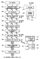
- Fig. 1 is a diagram showing an outside appearance of an image processing apparatus.
- Fig. 2 is a block diagram showing a flow of an image signal in an image processing unit 1008.
- Fig. 3 is a block diagram showing a printer unit 110.
- Fig. 4 is a block diagram showing an image processing unit 1008 for obtaining a gradation image.
- Fig. 5 is a flow chart showing an example of calibration control for a toner-low state.
- Fig. 6 is a diagram showing a display example of a display unit 218.
- Fig. 7 is a diagram showing a display example of a display unit 218.
- Fig. 8 is a diagram showing an example of a test pattern.
- Fig. 9 is a diagram showing a display example of a display unit 218.
- FIG. 10 is a diagram showing a display example of a display unit 218.
- Fig. 11 is a diagram showing a display example of a display unit 218.
- Fig. 12 is a flow chart of the processing for detecting a partial toner-low state.
- Fig. 13 is a flow chart of the processing for detecting a partial toner-low state.
- the present embodiment relates to an embodiment in which the present invention is applied to a full-color copying machine, but an application of the present invention is not limited to this embodiment.
- Fig. 1 is a diagram showing an outside appearance of an image processing apparatus according to the present embodiment. ⁇ Reader Unit 100>
- An original 1001 put on an original plate glass 1002 of a reader unit 100 is illuminated by a light source 1003, and the reflected light from the original 1001 produces an image in a CCD sensor 1005 through an optical system 1004.
- the CCD sensor 1005 is composed of a group of CCD line sensors of red, green and blue which are arranged in three lines, and color component signals of red, green and blue are produced for each line sensor.
- the read optical system unit moves in the direction of the arrow shown in Fig. 1 and converts the image of the original 1001 into an electrical signal for each line.
- a positioning member 1007 which abuts against one section of the original 1001 to prevent a slant position of the original 1001 and a reference white plate 1006 which determines a white level of the CCD sensor 1005 to make a shading correction of the CCD sensor 1005.
- An image signal obtained by the CCD sensor 1005 is image-processed by an image processing unit 1008, which is sent to a printer unit 110 where the image-processed image signal is processed in a printer control unit 1101.
- Fig. 2 is a block diagram showing a flow of an image signal in the image processing unit 1008.
- image signals outputted from the CCD sensor 1005 are inputted to an analog signal processing circuit 201 in which a gain and an offset of the image signal are adjusted. Thereafter, the image signals are converted into digital image signals of R1, G1 and B1 having each color of 8 bits by an A/D converter 202.
- the image signals of R1, G1 and B1 are inputted to a shading correction circuit 203, to which a well-known shading correction is made using a read signal of the reference white plate 1006 for each color.
- a clock generation unit 211 generates clocks (CLK) per one pixel unit.
- an address counter 212 counts CLK and generates and outputs a main scan address signal for each line.
- a decoder 213 decodes the main scan address signal to generate CCD drive signals of shift pulses, reset pulses and the like in a line unit, signals VE expressing an effective region among read signals corresponding to one line outputted by the CCD sensor 1005 and line synchronization signals HSYNC. It should be noted that the address counter 12 is cleared by HSYNC and starts with the counting of the main scan address for the next line.
- the respective line sensors of the CCD sensor 1005 are located to be spaced by a predetermined distance from each other in the sub scan direction. Therefore, a spatial shift in the sub scan direction is corrected by a line delay 204. Especially by line-delaying a R signal and a G signal to a B signal in the sub scan direction, spatial positions of the RGB signals are matched.
- An input masking circuit 205 converts color spaces (read color spaces) of input image signals determined based upon spectral characteristics of RGB filters of the CCD sensor 1005 into predetermined color spaces (for example, reference color spaces of sRGB or NTSC) according to a matrix calculation of the following expression (1).
- a Log conversion circuit 206 includes a lookup table ROM and converts luminance signals of R4, G4 and B4 into density signals of C0, M0 and Y0.
- a line delay memory 207 delays image signals of C0, M0 and Y0 by a line delay amount until determining signals such as UCR, FILTER and SEN are generated and outputted from the image signals of R4, G4 and B4, by a black character determining unit (not shown).
- a masking UCR circuit 208 extracts a black signal Bk from three-primary color signals of Y1, M1 and C1 inputted thereto. Further, the masking UCR circuit 208 performs a calculation of correcting color turbidity of a print color material of the printer unit 110 and sequentially outputs an image signal of Y2, M2, C2 or Bk2 for each read operation in a predetermined bit width (for example, 8 bits).
- a gamma correction circuit 209 corrects the image signal in density to adjust to an ideal gradation characteristic of the printer unit 110.
- an output filter 210 executes edge emphasis or smoothing processing to the image signal.
- the image signals of M4, C4, Y4 and Bk4 obtained by these processes are sent to the printer control unit 1101, wherein the image signal is converted into a pulse signal a pulse width of which is modulated, and density printing by the printer unit 110 is carried out.
- CPU 214 performs control or image processing of the reader unit 100 according to programs stored in ROM 216 using RAM 215 as a work memory.
- An operator inputs instructions or processing conditions to CPU 214 by an operation unit 217.
- a display unit 218 displays an operation condition of the image processing apparatus and the set processing condition.
- a surface of the photosensitive drum 1106 rotating in the direction of the arrow is uniformly charged by a primary charger 1110.
- the printer control unit 1101 outputs a pulse signal in accordance with an image data inputted by a laser driver.
- a laser light source 1102 outputs laser light in accordance with the pulse signal to be inputted.
- the laser light is reflected by a polygon mirror 1103 and a mirror 1104 and scans the charged surface of the photosensitive drum 1106.
- a static latent image is formed on the surface of the photosensitive drum 1106 by the scanning of the laser light.
- the static latent image formed on the surface of the photosensitive drum 1106 is developed with toner for each color by a developer 1105.
- one-component toner of a cartridge type with no stirring mechanism is used and developers for the respective colors are located around the photosensitive drum 1106 in the order of black Bk, yellow Y, cyan C and magenta M from the upstream.
- the developer in accordance with the image forming color comes close to the photosensitive drum 1106 to develop the static latent image.
- a print paper 1108 is wound around a transfer drum 1107 having one rotation for each color component, and toner images of the respective colors are transferred and superposed on the print paper 1108 by a sum of four rotations.
- the print paper 1108 is separated from the transfer drum 1107 and the toner is fixed thereon by a pair of fixing rollers 1109 to complete a print of the image data in full color.
- a surface potential sensor 1114 is located around the photosensitive drum 1106 upstream of the developer 1105 (place where the laser light is provided) for measuring a surface potential of the photosensitive drum 1106. Further, a cleaner 1111 is located around the photosensitive drum 1106 for cleaning the remaining toner, which is not transferred, on the photosensitive drum 1106. In addition, a LED light source 1112 and a photo diode 1113 are located around the photosensitive drum 1106 for detecting a reflection light amount of a toner patch formed on the photosensitive drum 1106.
- Fig. 3 is a block diagram showing the printer unit 110.
- the printer control unit 1101 comprises CPU 304, ROM 306, RAM 308, a test pattern memory unit 307, a density conversion circuit 311, LUT 301, a laser driver 303 and the like, and is capable of communicating with the reader unit 100 and a printer engine 300.
- CPU 304 controls an operation of the printer unit 110 and also controls a grid potential of the primary charger 1110 and development bias of the developer 1105.
- the printer engine 300 comprises the photosensitive drum 1106, a photo sensor 310 composed of the LED light source 1112 and the photo diode 1113, the primary charger 1110, the laser light source 1102, the surface potential sensor 1114, the developer 1105 and the like, which are located around the photosensitive drum 1106. Further, the printer engine 300 comprises an environment sensor 309 for measuring a water component amount (or temperature and relative humidity) in the air in the apparatus. ⁇ Image Processing Unit 1008>
- Fig. 4 is a block diagram showing the image processing unit 1008 for obtaining a gradation image.
- the image signal the gradation characteristic of which is converted by LUT 301 is converted into a pulse signal corresponding to a dot width by a pulse width modulation (PWM) circuit 401 of the laser driver 303, which is sent to a LD driver 402 controlling ON/OFF of the laser light source 1102.
- PWM pulse width modulation
- a gradation reproduction method by pulse width modulation is used for all the colors of Y, M, C and Bk.
- a static latent image the gradation of which is controlled with a change of a dot area and having a predetermined gradation characteristic is formed on the photosensitive drum 1106 by the scanning of the laser light outputted from the laser light source 1102, and a gradation image is reproduced through the processes of the aforementioned image development, transfer, and fixation.
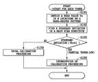
- Fig. 5 is a flow chart showing an example of the processing executed in the present embodiment, which is realized in cooperation of CPU 214 for controlling the reader unit 100 and CPU 304 for controlling the printer unit 110.
- the operation unit 217 which has received an operation of pushing down a mode setting button, for example, of "automatic gradation correction" provided in the operation unit 217 starts the processing of Fig. 5.
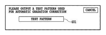
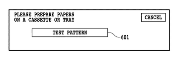
- the display unit 218 has a liquid crystal operation panel with a touch sensor (touch panel display) as shown in Fig. 6 or Fig. 7. ⁇ Explanation of Fig. 5>
- an output start button 601 of a test pattern (image data for detecting a partial toner-low state) shown in Fig. 6 appears on the display unit 218.
- the operation unit 217 outputs a test pattern shown in Fig. 8 from the printer unit 110 by receiving an operation of pushing down the output start button 601 of the test pattern.
- CPU 214 determines presence/absence of a print paper for forming the test pattern. In a case where it is determined at S502 that the print paper is not present, the process goes to S503, wherein CPU 214 displays a warning as shown in Fig. 7 on the display unit 218.
- the image processing apparatus has a plurality of print paper cassettes, and can select plural kinds of print paper sizes, for example, B4, A3, A4, B5 and the like.
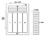
- the test pattern shown in Fig. 8 includes a band-shaped pattern 801 and a gradation pattern 802 for each toner kind (here, four colors of Y, M, C and Bk).
- the sizes of these patterns are set to be within a read range of the CCD sensor 1005.
- the band-shaped pattern 801 is used for detecting a partial toner-low state, and is set as a uniform pattern for basically outputting, not an intermediate density region where the density is unstable, but a high-density region.
- This band-shaped pattern is printed at least on an area covering an effective print region in the main scan direction in image formation.
- the high density region is preferably the maximum density which can be reproduced in the print unit, but in a case where reduction of the toner is preferable, the density corresponding to the order of 70% of the toner reproducing the maximum density is preferable.
- the density is, of course, not limited to 70% as long as it is at least 50%.
- a read button 901 shown in Fig. 9 appears on the display unit 218.
- the operation unit 217 reads data from the test pattern put on the original plate by receiving an operation of pushing down the read button 901.
- CPU 214 determines whether or not the reading of the test pattern is correctly made, based upon the data read at S504. In a case where at S505, CPU 214 determines that the correct reading is not made, for example, the inclination is large, the process goes to S506, wherein a warning as shown in Fig. 10 is displayed on the display unit 218.
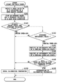
- CPU 214 detects whether or not a partial toner-low state occurs in each toner by using the read result of each band-shaped pattern 801. A detailed detection method will be explained with reference to Fig. 12.
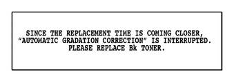
- the process goes to S509, wherein CPU 214 interrupts the calibration processing and displays a warning as shown in Fig. 11 on the display unit 218.
- the partial toner-low state in the main scan direction can be prevented without replacing a cartridge of Bk toner by a user removing, shaking, and reloading a cartridge.
- the display of warning messages may include information prompting the user to remove, shake, and reload a cartridge.
- Fig. 11 is shown on the basis of the determination that the partial toner-low state occurs in Bk toner.
- CPU 214 obtains a read value V n in N locations (N > 1) on the band-shaped pattern 801 in Fig. 8.
- CPU 214 finds a standard deviation S of the read value in the main scan direction from the N pieces of V n obtained at S1301 as below.
- the N pieces exist at positions which are uniformly distributed over the whole band-shaped pattern.
- the N pieces may not exist at positions which are uniformly distributed over the whole band-shaped pattern in a rigorous manner and the N pieces may exist at positions which are distributed over the whole band-shaped pattern in the main scan direction.
- CPU 214 finds an average value avg (V) of V n according to the following expression (2).
- CPU 214 finds a standard deviation S according to the following expression (4).
- the gradation test pattern of a single color of C, M, Y or Bk is formed to correct a gradation density characteristic in regard to each single color to a target reproduction characteristic.
- a test pattern in which C, M, Y and Bk are mixed may be formed, which is applied to calibration for adjusting a color reproduction characteristic of the mixed color.
- the masking UCR circuit is changed to 3D (multi-dimension) LUT for performing direct mapping, and values corresponding to grid points of 3D (multi-dimension) LUT are targets adjusted by calibration.
- CPU 214 finds an average value avg (V) of the read value in the main scan direction from N pieces of V n obtained at S1401 and the standard deviation S according to the expressions (2) and (3).
- the determination that the toner is in the entire toner-low state may be made by sensor information of a toner remaining amount detecting sensor (not shown) having a cartridge of the toner.
- CPU 214 executes usual calibration processing.
- CPU 214 may interrupt the calibration processing.
- CPU 214 specifies an occurrence position of the partial toner-low state. For example, CPU 214 may compare the average value avg (V) with V n and specify a location where the variation close to the standard deviation occurs, as the occurrence position of the partial toner-low state.
- CPU 214 analyses the occurrence position of the partial toner-low state specified at S1403. Especially the occurrence position of the partial toner-low state specified at S1403 is compared with a position where the gradation pattern 802 is formed. In addition, CPU 214 analyses whether or not the occurrence position of the partial toner-low state specified at S1403 is close to the gradation pattern 802 in the main scan direction.
- CPU 214 determines whether or not the position of the partial toner-low state is close to the position where the gradation pattern 802 is formed, based upon the analysis performed at S1404. In a case where at S1405 it is determined that the position of the partial toner-low state is close to the position where the gradation pattern 802 is formed, the process goes to S1305. At S1305, CPU 214 interrupts the calibration processing. On the other hand, in a case where at S1405 it is determined that the position of the partial toner-low state is not close to the position where the gradation pattern 802 is formed, the process goes to S1304. At S1304, CPU 214 executes usual calibration processing.
- the position of partial toner-low state is the left end of the Bk band-shaped pattern 801, for example, it may be determined that partial toner-low is not occurred in a main scan position where Bk gradation pattern 802 is formed.
- the formed Bk gradation pattern adequately shows the reproduction characteristic of the Bk printer unit 110, and thus usual calibration processing can be executed.
- the position of partial toner-low state is the right end of the Bk band-shaped pattern 801
- the test pattern is re-formed by replacing the position of the gradation pattern of the certain color and the forming position of the band-shaped pattern of the another color, thereby allowing continuous execution of calibration.
- the photosensitive drum having a relative large bore diameter is used. Further, for accurately and efficiently obtaining the density information, patches of the same color are formed at positions in point symmetry to the center of the photosensitive drum 1106 in consideration of eccentricity of the photosensitive drum 1106, and the density information is found by averaging a plurality of values obtained by measuring these patches.
- the second control system is provided with control which forms a patch in a non-image region in the middle of the usual image formation and detects the density to correct table data of LUT 301 as needed. Since a region on the photosensitive drum 1106 corresponding to a gap portion between print papers wound around the transfer drum 1107 corresponds to the non-image region, the patch is formed in that region.
- patches of the same color are, as described above, formed in positions in point symmetry to the center of the photosensitive drum 1106.
- T the density values are compared from the read values of these patches and are largely different from each other (the density values are different from each other by over predetermined threshold value T)
- the patch to be compared is a patch outputting, not an intermediate density region which is basically unstable, but a high density region.
- the main scan positions between patches to be compared are very away from each other, there is the possibility that both of the patches are in the partial toner-low state. In this case, since the density difference does not occur largely, it results in being incapable of detecting the partial toner-low state.
- At least one patch is outputted in a position where the toner remaining amount detecting sensor with a cartridge (not shown) can cover the remaining amount detection with some degrees of accuracy.
- This patch is defined as a reference patch.
- the toner-low state in the reference patch position is detected by the toner remaining amount detecting sensor, and the partial toner-low state in the other patch position can be determined based upon a density difference from the reference patch.
- the test pattern is shown in Fig. 8 with the band-shaped pattern 801, but since it is only required to obtain the read value V n in N locations (N > 1) in the main scan direction, the test pattern is not necessarily band-shaped. Description is made in such a manner that the band-shaped pattern 801 and the gradation pattern 802 exist on the same paper, but the embodiment is not limited thereto. For example, the band-shaped pattern and the gradation pattern may exist on the paper where images are continuously formed.
- the calibration may be controlled by detecting the partial toner-low state from information of the plurality of the sensors.
- aspects of the present invention can also be realized by a computer of a system or apparatus (or devices such as a CPU or MPU) that reads out and executes a program recorded on a memory device to perform the functions of the above-described embodiment(s), and by a method, the steps of which are performed by a computer of a system or apparatus by, for example, reading out and executing a program recorded on a memory device to perform the functions of the above-described embodiment(s).
- the program is provided to the computer for example via a network or from a recording medium of various types serving as the memory device (e.g., computer-readable medium).
Landscapes
- Physics & Mathematics (AREA)
- General Physics & Mathematics (AREA)
- Engineering & Computer Science (AREA)
- Multimedia (AREA)
- Signal Processing (AREA)
- Microelectronics & Electronic Packaging (AREA)
- Control Or Security For Electrophotography (AREA)
- Facsimile Image Signal Circuits (AREA)
- Measurement Of Levels Of Liquids Or Fluent Solid Materials (AREA)
- Dry Development In Electrophotography (AREA)
- Image Processing (AREA)
Priority Applications (1)
| Application Number | Priority Date | Filing Date | Title |
|---|---|---|---|
| US12/739,045 US8422894B2 (en) | 2009-04-10 | 2010-03-24 | Image processing apparatus, image processing method and program for controlling calibration |
Applications Claiming Priority (2)
| Application Number | Priority Date | Filing Date | Title |
|---|---|---|---|
| JP2009095987A JP5230510B2 (ja) | 2009-04-10 | 2009-04-10 | 画像処理装置、画像処理方法、およびプログラム |
| JP2009-095987 | 2009-04-10 |
Publications (1)
| Publication Number | Publication Date |
|---|---|
| WO2010116631A1 true WO2010116631A1 (en) | 2010-10-14 |
Family
ID=42935932
Family Applications (1)
| Application Number | Title | Priority Date | Filing Date |
|---|---|---|---|
| PCT/JP2010/002048 Ceased WO2010116631A1 (en) | 2009-04-10 | 2010-03-24 | Image processing apparatus, image processing method and program |
Country Status (3)
| Country | Link |
|---|---|
| US (1) | US8422894B2 (enExample) |
| JP (1) | JP5230510B2 (enExample) |
| WO (1) | WO2010116631A1 (enExample) |
Families Citing this family (8)
| Publication number | Priority date | Publication date | Assignee | Title |
|---|---|---|---|---|
| JP2010274616A (ja) * | 2009-06-01 | 2010-12-09 | Konica Minolta Business Technologies Inc | 画像処理システム、画像処理装置、画像形成装置及びプログラム |
| JP5782743B2 (ja) * | 2011-02-23 | 2015-09-24 | 富士ゼロックス株式会社 | 制御装置及び画像形成装置 |
| JP5850300B2 (ja) * | 2011-04-22 | 2016-02-03 | 株式会社リコー | 画像形成装置 |
| JP2014033306A (ja) * | 2012-08-02 | 2014-02-20 | Canon Inc | 画像処理装置、画像処理方法ならびにプログラム |
| US9631977B2 (en) * | 2013-12-17 | 2017-04-25 | Xerox Corporation | Device calibration using augmented data with hadamard variation |
| JP6639152B2 (ja) * | 2015-08-24 | 2020-02-05 | キヤノン株式会社 | 画像形成装置 |
| WO2018221408A1 (ja) * | 2017-05-30 | 2018-12-06 | 京セラドキュメントソリューションズ株式会社 | 画像形成装置 |
| CN113630516B (zh) * | 2021-08-02 | 2025-03-11 | 珠海奔图电子有限公司 | 画像校正方法、图像形成装置及存储介质 |
Citations (6)
| Publication number | Priority date | Publication date | Assignee | Title |
|---|---|---|---|---|
| JPH07264412A (ja) * | 1994-03-25 | 1995-10-13 | Canon Inc | 画像形成装置 |
| JPH08114985A (ja) * | 1994-10-17 | 1996-05-07 | Purintonikusu:Kk | 現像装置 |
| JPH09186899A (ja) * | 1995-12-28 | 1997-07-15 | Ricoh Co Ltd | カラーバランス調整前処理方法 |
| JP2001350302A (ja) * | 2000-06-08 | 2001-12-21 | Nec Niigata Ltd | 電子写真プリンタの印刷濃度検出装置および印刷濃度調整装置ならびに印刷濃度検出方法および印刷濃度調整方法 |
| JP2004038048A (ja) * | 2002-07-05 | 2004-02-05 | Canon Inc | 画像形成装置 |
| JP2007187930A (ja) * | 2006-01-13 | 2007-07-26 | Fuji Xerox Co Ltd | 画像形成装置及び膜厚測定方法 |
Family Cites Families (10)
| Publication number | Priority date | Publication date | Assignee | Title |
|---|---|---|---|---|
| US4348099A (en) * | 1980-04-07 | 1982-09-07 | Xerox Corporation | Closed loop control of reproduction machine |
| US4318610A (en) * | 1980-04-21 | 1982-03-09 | Xerox Corporation | Control system for an electrophotographic printing machine |
| US5081491A (en) * | 1990-12-04 | 1992-01-14 | Xerox Corporation | Toner maintenance subsystem for a printing machine |
| JPH06102735A (ja) * | 1992-09-24 | 1994-04-15 | Toshiba Corp | 画像形成装置 |
| JPH0895368A (ja) * | 1994-09-29 | 1996-04-12 | Ricoh Co Ltd | 画像形成装置 |
| JP2004004967A (ja) * | 1995-10-31 | 2004-01-08 | Ricoh Co Ltd | 現像装置 |
| JP3955079B2 (ja) * | 1995-11-14 | 2007-08-08 | 株式会社リコー | 現像装置 |
| US5978506A (en) * | 1995-12-28 | 1999-11-02 | Ricoh & Company, Ltd. | Colorant-independent color balancing methods and systems |
| JP2001290356A (ja) | 2000-04-06 | 2001-10-19 | Canon Inc | 電子写真画像形成装置 |
| KR100449726B1 (ko) * | 2002-06-11 | 2004-09-22 | 삼성전자주식회사 | 화상형성장치의 토너소진 검출방법 |
-
2009
- 2009-04-10 JP JP2009095987A patent/JP5230510B2/ja active Active
-
2010
- 2010-03-24 US US12/739,045 patent/US8422894B2/en not_active Expired - Fee Related
- 2010-03-24 WO PCT/JP2010/002048 patent/WO2010116631A1/en not_active Ceased
Patent Citations (6)
| Publication number | Priority date | Publication date | Assignee | Title |
|---|---|---|---|---|
| JPH07264412A (ja) * | 1994-03-25 | 1995-10-13 | Canon Inc | 画像形成装置 |
| JPH08114985A (ja) * | 1994-10-17 | 1996-05-07 | Purintonikusu:Kk | 現像装置 |
| JPH09186899A (ja) * | 1995-12-28 | 1997-07-15 | Ricoh Co Ltd | カラーバランス調整前処理方法 |
| JP2001350302A (ja) * | 2000-06-08 | 2001-12-21 | Nec Niigata Ltd | 電子写真プリンタの印刷濃度検出装置および印刷濃度調整装置ならびに印刷濃度検出方法および印刷濃度調整方法 |
| JP2004038048A (ja) * | 2002-07-05 | 2004-02-05 | Canon Inc | 画像形成装置 |
| JP2007187930A (ja) * | 2006-01-13 | 2007-07-26 | Fuji Xerox Co Ltd | 画像形成装置及び膜厚測定方法 |
Also Published As
| Publication number | Publication date |
|---|---|
| JP2010249861A (ja) | 2010-11-04 |
| JP5230510B2 (ja) | 2013-07-10 |
| US8422894B2 (en) | 2013-04-16 |
| US20110194862A1 (en) | 2011-08-11 |
Similar Documents
| Publication | Publication Date | Title |
|---|---|---|
| EP2408189B1 (en) | Image processing apparatus and its control method | |
| JP5188313B2 (ja) | 画像形成装置及びその濃度階調制御方法 | |
| JP3441994B2 (ja) | 画像処理装置及びその制御方法 | |
| WO2010116631A1 (en) | Image processing apparatus, image processing method and program | |
| JP6572577B2 (ja) | 画像形成装置及び位置調整方法並びに位置調整プログラム | |
| JP4371803B2 (ja) | 画像形成装置 | |
| JP3854965B2 (ja) | 画像形成装置 | |
| JP5094100B2 (ja) | 画像形成装置 | |
| JP5300418B2 (ja) | 画像形成装置 | |
| US8531745B2 (en) | Image formation density correction in image forming apparatus | |
| JP2008139856A (ja) | 画像形成装置およびその制御方法 | |
| JP3885056B2 (ja) | 画像処理装置およびその制御方法 | |
| JPH08287217A (ja) | 画像記録装置およびその方法 | |
| JP2011175099A (ja) | 画像形成装置及びその制御方法 | |
| JPH08289149A (ja) | 画像記録装置およびその方法 | |
| JP2001180090A (ja) | 画像形成システム、画像出力装置およびキャリブレーション方法 | |
| JP2008154115A (ja) | 画像形成装置及び補正方法 | |
| US11953852B2 (en) | Image forming apparatus | |
| JP4890910B2 (ja) | 画像形成装置 | |
| JP2003195583A (ja) | 画像形成装置 | |
| JPH1198358A (ja) | 画像処理装置及び画像処理方法 | |
| JP2010019968A (ja) | 画像形成装置、画像補正方法、画像補正プログラム及び記録媒体 | |
| JP2004064358A (ja) | 画像処理方法およびその装置 | |
| JPH08289150A (ja) | 画像記録装置およびその方法 | |
| JP2022117153A (ja) | 画像形成装置 |
Legal Events
| Date | Code | Title | Description |
|---|---|---|---|
| WWE | Wipo information: entry into national phase |
Ref document number: 12739045 Country of ref document: US |
|
| 121 | Ep: the epo has been informed by wipo that ep was designated in this application |
Ref document number: 10761339 Country of ref document: EP Kind code of ref document: A1 |
|
| NENP | Non-entry into the national phase |
Ref country code: DE |
|
| 122 | Ep: pct application non-entry in european phase |
Ref document number: 10761339 Country of ref document: EP Kind code of ref document: A1 |