WO2010113779A1 - 半導体装置 - Google Patents
半導体装置 Download PDFInfo
- Publication number
- WO2010113779A1 WO2010113779A1 PCT/JP2010/055321 JP2010055321W WO2010113779A1 WO 2010113779 A1 WO2010113779 A1 WO 2010113779A1 JP 2010055321 W JP2010055321 W JP 2010055321W WO 2010113779 A1 WO2010113779 A1 WO 2010113779A1
- Authority
- WO
- WIPO (PCT)
- Prior art keywords
- gate
- semiconductor device
- electrode
- source
- finger
- Prior art date
- Legal status (The legal status is an assumption and is not a legal conclusion. Google has not performed a legal analysis and makes no representation as to the accuracy of the status listed.)
- Ceased
Links
Images






Classifications
-
- H—ELECTRICITY
- H10—SEMICONDUCTOR DEVICES; ELECTRIC SOLID-STATE DEVICES NOT OTHERWISE PROVIDED FOR
- H10D—INORGANIC ELECTRIC SEMICONDUCTOR DEVICES
- H10D64/00—Electrodes of devices having potential barriers
- H10D64/20—Electrodes characterised by their shapes, relative sizes or dispositions
- H10D64/27—Electrodes not carrying the current to be rectified, amplified, oscillated or switched, e.g. gates
- H10D64/311—Gate electrodes for field-effect devices
- H10D64/411—Gate electrodes for field-effect devices for FETs
- H10D64/511—Gate electrodes for field-effect devices for FETs for IGFETs
- H10D64/517—Gate electrodes for field-effect devices for FETs for IGFETs characterised by the conducting layers
- H10D64/519—Gate electrodes for field-effect devices for FETs for IGFETs characterised by the conducting layers characterised by their top-view geometrical layouts
-
- H—ELECTRICITY
- H10—SEMICONDUCTOR DEVICES; ELECTRIC SOLID-STATE DEVICES NOT OTHERWISE PROVIDED FOR
- H10D—INORGANIC ELECTRIC SEMICONDUCTOR DEVICES
- H10D64/00—Electrodes of devices having potential barriers
- H10D64/20—Electrodes characterised by their shapes, relative sizes or dispositions
- H10D64/23—Electrodes carrying the current to be rectified, amplified, oscillated or switched, e.g. sources, drains, anodes or cathodes
- H10D64/251—Source or drain electrodes for field-effect devices
- H10D64/257—Source or drain electrodes for field-effect devices for lateral devices wherein the source or drain electrodes are characterised by top-view geometrical layouts, e.g. interdigitated, semi-circular, annular or L-shaped electrodes
-
- H—ELECTRICITY
- H10—SEMICONDUCTOR DEVICES; ELECTRIC SOLID-STATE DEVICES NOT OTHERWISE PROVIDED FOR
- H10D—INORGANIC ELECTRIC SEMICONDUCTOR DEVICES
- H10D84/00—Integrated devices formed in or on semiconductor substrates that comprise only semiconducting layers, e.g. on Si wafers or on GaAs-on-Si wafers
- H10D84/01—Manufacture or treatment
-
- H—ELECTRICITY
- H10—SEMICONDUCTOR DEVICES; ELECTRIC SOLID-STATE DEVICES NOT OTHERWISE PROVIDED FOR
- H10D—INORGANIC ELECTRIC SEMICONDUCTOR DEVICES
- H10D84/00—Integrated devices formed in or on semiconductor substrates that comprise only semiconducting layers, e.g. on Si wafers or on GaAs-on-Si wafers
- H10D84/80—Integrated devices formed in or on semiconductor substrates that comprise only semiconducting layers, e.g. on Si wafers or on GaAs-on-Si wafers characterised by the integration of at least one component covered by groups H10D12/00 or H10D30/00, e.g. integration of IGFETs
- H10D84/82—Integrated devices formed in or on semiconductor substrates that comprise only semiconducting layers, e.g. on Si wafers or on GaAs-on-Si wafers characterised by the integration of at least one component covered by groups H10D12/00 or H10D30/00, e.g. integration of IGFETs of only field-effect components
- H10D84/83—Integrated devices formed in or on semiconductor substrates that comprise only semiconducting layers, e.g. on Si wafers or on GaAs-on-Si wafers characterised by the integration of at least one component covered by groups H10D12/00 or H10D30/00, e.g. integration of IGFETs of only field-effect components of only insulated-gate FETs [IGFET]
-
- H—ELECTRICITY
- H10—SEMICONDUCTOR DEVICES; ELECTRIC SOLID-STATE DEVICES NOT OTHERWISE PROVIDED FOR
- H10W—GENERIC PACKAGES, INTERCONNECTIONS, CONNECTORS OR OTHER CONSTRUCTIONAL DETAILS OF DEVICES COVERED BY CLASS H10
- H10W20/00—Interconnections in chips, wafers or substrates
- H10W20/40—Interconnections external to wafers or substrates, e.g. back-end-of-line [BEOL] metallisations or vias connecting to gate electrodes
- H10W20/482—Interconnections external to wafers or substrates, e.g. back-end-of-line [BEOL] metallisations or vias connecting to gate electrodes for individual devices provided for in groups H10D8/00 - H10D48/00, e.g. for power transistors
- H10W20/483—Interconnections over air gaps, e.g. air bridges
-
- H—ELECTRICITY
- H10—SEMICONDUCTOR DEVICES; ELECTRIC SOLID-STATE DEVICES NOT OTHERWISE PROVIDED FOR
- H10W—GENERIC PACKAGES, INTERCONNECTIONS, CONNECTORS OR OTHER CONSTRUCTIONAL DETAILS OF DEVICES COVERED BY CLASS H10
- H10W20/00—Interconnections in chips, wafers or substrates
- H10W20/40—Interconnections external to wafers or substrates, e.g. back-end-of-line [BEOL] metallisations or vias connecting to gate electrodes
- H10W20/482—Interconnections external to wafers or substrates, e.g. back-end-of-line [BEOL] metallisations or vias connecting to gate electrodes for individual devices provided for in groups H10D8/00 - H10D48/00, e.g. for power transistors
- H10W20/484—Interconnections having extended contours, e.g. pads having mesh shape or interconnections comprising connected parallel stripes
Definitions
- the present invention relates to a multi-finger (comb structure) transistor, and more particularly to a multi-finger transistor for use in the microwave region.
- FIG. 1 is a schematic diagram for explaining the structure of a multi-finger FET (Field Effect Transistor) according to a technique related to the present invention.
- This multi-finger FET includes a gate portion, a source portion, and a drain portion.
- the gate portion includes a gate electrode pad 1, a gate bus bar 4, and a plurality of gate fingers 5.
- the source part includes a source electrode pad 2, a plurality of source electrodes 6, and a plurality of via holes 3.
- the drain part includes a drain electrode pad 8 and a plurality of drain electrodes 7.
- the plurality of source electrodes 6 and the plurality of drain electrodes 7 are alternately arranged one by one.
- a single gate finger 5 is disposed between the adjacent source electrode 6 and drain electrode 7.
- the gate electrode pad 1 is connected to a plurality of gate fingers 5 via a gate bus bar 4.
- the source electrode pad 2 is connected to a plurality of via holes 3 through an air bridge.
- the plurality of via holes 3 are grounded.
- the plurality of via holes 3 are respectively connected to the plurality of source electrodes 6.
- the drain electrode pad 8 is connected to a plurality of drain electrodes 7.
- each gate finger 5 is represented as C and R, respectively.
- the finger length of the gate finger 5 is represented as Lw.
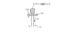
- FIG. 2 is a schematic diagram for explaining a coordinate system set in a gate portion in a multi-finger FET according to a technique related to the present invention.
- This gate portion is equivalent to a part extracted from the gate portion in FIG.
- the gate portion includes a gate electrode pad 9, a gate bus bar 10, and a plurality of gate fingers 11. That is, the gate electrode pad 9, the gate bus bar 10 and the plurality of gate fingers 11 in FIG. 2 correspond to the gate electrode pad 1, the gate bus bar 4 and the plurality of gate fingers 5 in FIG.
- the base position of the gate finger 11 connected to the gate bus bar 10 is the origin, and the length direction of the gate finger 11 is the x-axis.
- the coordinates of the tip of the gate finger 11 are Lw.
- the current and voltage at an arbitrary point of the gate finger are not uniform. This means that the device characteristics of the gate finger vary depending on the location, and the device characteristics of the multi-finger FET are likely to vary.
- the current and voltage in the gate finger are not uniform according to the distributed constant expression. Accordingly, the source inductor viewed from the gate finger changes depending on the position of the gate finger viewed from. As a result, there is a problem of affecting the device gain characteristic in the multi-finger FET according to the related art.
- the source inductor that contributes to the decrease in FET gain.
- the via hole is connected only on one side of the source electrode. Therefore, the source inductor viewed from the gate finger also changes depending on where the gate finger is viewed. In particular, the increase in the source inductor that can be seen from the end points of the gate fingers is a cause of greatly degrading the device gain characteristics. This is also a problem that exists in the multi-finger FET according to the related art.
- the gate feed line becomes a closed circuit.
- loop oscillation may occur and the multi-finger FET may become unstable. This is also a problem that exists in the multi-finger FET according to the related art.
- Patent Document 1 Japanese Unexamined Patent Publication No. 2000-1382366 discloses a description relating to a semiconductor device.
- This semiconductor device uses a field effect transistor having a comb-shaped gate electrode and drain electrode in which a plurality of source electrodes arranged on the same axis are connected by a conductor.
- This semiconductor device includes a via hole in which each ground electrode to which the source electrode located at both ends of each source electrode is connected correspondingly is installed.
- each via hole has an elliptical shape.
- An object of the present invention is to provide a multi-finger FET in which the source inductor viewed from each point of the gate finger is uniform and stable.
- the semiconductor device includes a source electrode, a drain electrode, a gate electrode, and a gate feed line.
- the gate electrode is disposed between the source electrode and the drain electrode.
- the gate power supply line is connected to both ends of the gate electrode.
- the source inductor viewed from each point of the gate finger is uniform and stable. Therefore, high gain of the FET is realized in the microwave and millimeter wave bands.
- FIG. 1 is a schematic diagram for explaining the structure of a multi-finger FET according to a technique related to the present invention.
- FIG. 2 is a schematic diagram for explaining a coordinate system set in a gate portion in a multi-finger FET according to a technique related to the present invention.
- FIG. 3 is a schematic diagram for explaining the overall structure of the multi-finger FET according to the first embodiment of the present invention.
- FIG. 4 is a schematic diagram for explaining a coordinate system set in the gate portion of the multi-finger FET according to the first embodiment of the present invention.
- FIG. 5 is a schematic view for explaining the overall structure of the semiconductor device according to the second embodiment of the present invention.
- FIG. 1 is a schematic diagram for explaining the structure of a multi-finger FET according to a technique related to the present invention.
- FIG. 2 is a schematic diagram for explaining a coordinate system set in a gate portion in a multi-finger FET according to a technique related to the present invention.
- FIG. 6 is a graph showing the result of obtaining the gain characteristic (Gain) in the 38 GHz band of the high frequency FET according to the value of the source inductor (parasitic inductor).
- FIG. 7 is a schematic view for explaining the overall structure of the semiconductor device according to the third embodiment of the present invention.
- FIG. 8A is a circuit diagram for explaining a closed circuit when the ladder circuit is removed from the semiconductor device according to the present embodiment.
- FIG. 8B is a graph for explaining the result of calculating the phase difference in the closed circuit when the ladder circuit is removed from the semiconductor device according to the present embodiment.
- FIG. 9A is a circuit diagram for explaining the closed circuit when the semiconductor device according to the present embodiment, that is, the ladder circuit is provided.
- FIG. 10 is a schematic diagram for explaining a structure in an example of an MMIC (high frequency monolithic integrated circuit) based on a multi-finger structure of a semiconductor device according to the present invention.
- MMIC high frequency monolithic integrated circuit
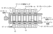
- FIG. 3 is a schematic view for explaining the overall structure of the semiconductor device according to the first embodiment of the present invention.
- This semiconductor device is a multi-finger FET, and includes a source part, a gate part, and a drain part.
- the source section includes two source electrode pads 13, a plurality of via holes 14, and a plurality of source electrodes 17.
- the gate portion includes a gate electrode pad 12, a gate bus bar 15, and a plurality of gate fingers 16.
- the gate bus bar 15 has two ends.
- the drain portion includes a drain electrode pad 19, a plurality of air bridges 57, and a plurality of drain electrodes 18.
- the numbers of the source electrode 17, the drain electrode 18 and the gate fingers 16 are 5, 6, and 10 in FIG. 3, respectively, but these numbers are merely examples and do not limit the present invention. .
- the gate finger 16 operates as a gate electrode.
- the gate bus bar 15 operates as a gate feed line.
- the via hole 14 is grounded and operates as a ground portion.
- the plurality of source electrodes 17 and the plurality of drain electrodes 18 are alternately arranged one by one.
- One gate finger 16 is disposed between the adjacent source electrode 17 and drain electrode 18.
- the two source electrode pads 13 are connected to a plurality of via holes 14.
- the plurality of via holes 14 are grounded.
- one end is connected to one source electrode pad 13 and the other end is connected to the other source electrode pad 13.
- the gate electrode pad 12 is connected in the middle of the gate bus bar 15. From the position where the gate electrode pad 12 is connected to one end of the gate bus bar 15 is referred to as one end of the gate bus bar 15. Similarly, the portion from the position where the gate electrode pad 12 is connected to the other end is referred to as the other end of the gate bus bar 15.
- the two ends of the gate bus bar 15 are arranged along a sequence of the plurality of source electrodes 17, the plurality of drain electrodes 18, and the plurality of gate fingers 16, respectively. Both ends of the plurality of gate fingers 16 are connected to one end and the other end of the gate bus bar 15, respectively. Therefore, the entire potential of all gate fingers 16 is the same potential.
- the drain electrode pad 19 is connected to the first drain electrode 18.
- the first drain electrode 18 is connected to the first air bridge 57.
- the first air bridge 57 is connected to the second drain electrode 18.
- the first air bridge 57 straddles the two gate fingers 16 and the one source electrode 17 arranged between the first drain electrode 18 and the second drain electrode 18.
- the plurality of drain electrodes 18 and the plurality of air bridges 57 are alternately connected one by one, and each air bridge 57 is disposed between two drain electrodes 18 connected to both ends thereof. It straddles two gate fingers 16 and one source electrode 17.
- FIG. 4 is a schematic diagram for explaining a coordinate system set in the gate portion of the multi-finger FET according to the present embodiment.
- This gate portion is equivalent to a part extracted from the gate portion in FIG.
- the gate portion includes a gate electrode pad 20, a gate bus bar 21, and a plurality of gate fingers 22. That is, the gate electrode pad 20, the gate bus bar 21 and the plurality of gate fingers 22 in FIG. 4 correspond to the gate electrode pad 12, the gate bus bar 15 and the plurality of gate fingers 16 in FIG.
- one end of the gate finger 22, that is, one base position connected to the gate bus bar 21 is an origin, and the length direction of the gate finger 22 is an x-axis.
- the coordinate of the other end of the gate finger 22 is Lw.
- Lw is the length of the gate finger 22.
- the gate resistance can be reduced to 1 ⁇ 4 of the related technical structure.
- the voltage is uniform over the entire area of the gate finger, and the influence of variations in device characteristics is small.
- FIG. 5 is a schematic view for explaining the overall structure of the semiconductor device according to the second embodiment of the present invention.
- This semiconductor device is obtained by changing the number of source electrodes 28 in the semiconductor device according to the first embodiment to one. As a result, the number of drain electrodes 29 is changed to two, and the number of gate fingers 27 is changed to two.
- the present embodiment is the minimum configuration of a multi-finger FET as a semiconductor device according to the present invention.
- the semiconductor device further includes two source electrode pads 25, two via holes 26, a gate electrode pad 23, a gate bus bar 24, a drain electrode pad 30, and an air bridge 58.
- the two source electrode pads 25, the two via holes 26, the gate electrode pad 23, the gate bus bar 24 and the drain electrode pad 30 in FIG. 5 are the plurality of via holes 14, the gate electrode pad 12, the gate bus bar 15 and the drain electrode pad in FIG. 19 respectively.
- the two via holes 26 connected to the source electrode 28 are disposed at both ends of the source electrode 28.
- the source inductor can be reduced, and at the same time, the influence of the source inductor seen from each point of the gate finger 27 can be reduced.
- FIG. 6 is a graph showing the result of obtaining the gain characteristic (Gain) in the 38 GHz band of the high frequency FET according to the value of the source inductor (parasitic inductor).
- the horizontal axis represents the value L of the source inductor
- the vertical axis represents the gain characteristic.
- the value of the source inductor in the related art semiconductor device was 0.08 nH. It can be seen from the graph of FIG. 6 that if the value of the source inductor is halved to 0.04 nH, the gain characteristic can be brought close to its ideal value of about 6.8 dB.
- the multi-finger FET according to the present invention can Gain characteristics higher than those of the technology can be obtained.
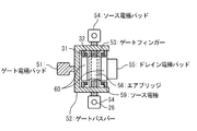
- FIG. 7 is a schematic view for explaining the overall structure of the semiconductor device according to the third embodiment of the present invention.
- This semiconductor device is equivalent to a multi-finger FET according to the second embodiment added with a ladder circuit.
- the 7 includes a gate electrode pad 51, a gate bus bar 52, two gate fingers 53, two source electrode pads 54, a source electrode 59, a drain electrode pad 55, and two drain electrodes. 60, an air bridge 56, a resistor 31, and a capacitor 32 with a via hole.
- the gate electrode pad 51, the gate bus bar 52, the two gate fingers 53, the two source electrode pads 54, the source electrode 59, the drain electrode pad 55, the two drain electrodes 60, and the air bridge 56 of FIG. Correspond to each.
- the resistor 31 and the capacitor 32 with a via hole correspond to the ladder circuit in the present embodiment.
- the capacitor 32 with a via hole is grounded at the via hole.
- This ladder circuit is obtained by connecting a resistor 31 and a capacitor 32 with a via hole in series. This ladder circuit is connected to the gate finger 53 in parallel to suppress and avoid loop oscillation.
- FIG. 8A is a circuit diagram for explaining a closed circuit when the ladder circuit is removed from the semiconductor device according to the present embodiment.
- the closed circuit includes three gate bus bars 33 and one gate finger 34.
- the three gate bus bars 33 in FIG. 8A correspond to the two ends of the gate bus bar 52 and the gate electrode pad 51 in FIG.
- the gate finger 34 in FIG. 8A corresponds to the gate finger 53 in FIG.
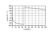
- FIG. 8B is a graph for explaining the result of calculating the phase difference in the closed circuit when the ladder circuit is removed from the semiconductor device according to the present embodiment.
- the horizontal axis represents frequency and the vertical axis represents phase difference.
- phase difference is around 180 degrees. This phase difference is determined by a combination of lengths on the layout of the gate bus bar and the gate finger.
- FIG. 9A is a circuit diagram for explaining a closed circuit when the semiconductor device according to the present embodiment, that is, a ladder circuit is provided.
- the closed circuit includes three gate bus bars 35, one gate finger 36, and two ladder circuits.
- Each of the two ladder circuits includes a resistor 37 and a grounded capacitor 38.
- the three gate bus bars 35 in FIG. 9A correspond to the two ends of the gate bus bar 52 and the gate electrode pad 51 in FIG.
- the gate finger 36 in FIG. 9A corresponds to the gate finger 53 in FIG.
- the resistor 37 and the grounded capacitor 38 in FIG. 9A correspond to the resistor 31 and the capacitor 32 with a via hole in FIG.
- FIG. 9B is a circuit diagram for explaining the result of calculating the phase difference in the closed circuit when the semiconductor device according to the present embodiment, that is, the ladder circuit is provided.
- the horizontal axis represents frequency and the vertical axis represents phase difference.
- FIG. 10 is a schematic diagram for explaining a structure in an example of an MMIC (high frequency monolithic integrated circuit) based on a multi-finger structure of a semiconductor device according to the present invention.
- This MMIC includes a bias circuit 39, a multi-finger FET according to the second embodiment of the present invention, an interstage signal circuit 40, a multi-finger FET according to the first embodiment of the present invention, an output matching circuit 41, And a plurality of capacitors 42a to 42d.
- the bias circuit 39 is connected to the gate electrode pad 23 in the multi-finger FET according to the second embodiment of the present invention.
- the drain electrode pad 30 in the multi-finger FET according to the second embodiment of the present invention is connected to the first capacitor 42 a and the interstage signal circuit 40.
- the interstage signal circuit 40 is connected to the gate electrode pad 12 in the multi-finger FET according to the first embodiment of the present invention via the second capacitor 42b.
- the drain electrode pad 19 in the multi-finger FET according to the first embodiment of the present invention is connected to the third capacitor 42c.
- the drain electrode pad 19 in the multi-finger FET according to the first embodiment of the present invention is connected to the fourth capacitor 42 d and the output matching circuit 41.
- high gain characteristics can be achieved in the frequency region from the microwave band to the millimeter wave band. At the same time, development to a high gain MMIC is also possible.
- the multi-finger structure of the present invention is a compound semiconductor such as GaAs (gallium arsenide), InP (indium phosphide), GaN (gallium nitride), SiC (silicon carbide), ZnO (zinc oxide), etc. (Complementary Metal Oxide Semiconductor), SiGe (silicon germanium) and other Si (silicon) based semiconductors can be used for high gain FETs and MMICs.
- GaAs gallium arsenide
- InP indium phosphide
- GaN gallium nitride
- SiC silicon carbide
- ZnO zinc oxide
Landscapes
- Junction Field-Effect Transistors (AREA)
- Semiconductor Integrated Circuits (AREA)
Abstract
Description
∂V2(x)/∂x=CR∂V(x)/∂t
V(0)=V0
I(Lw)=0
図3は、本発明の第1の実施形態による半導体装置の全体的な構造について説明するための概略図である。この半導体装置は、マルチフィンガーFETであって、ソース部と、ゲート部と、ドレイン部とを具備する。ここで、ソース部は、2つのソース電極パッド13と、複数のビアホール14と、複数のソース電極17とを具備する。ゲート部は、ゲート電極パッド12と、ゲートバスバー15と、複数のゲートフィンガー16とを具備する。ゲートバスバー15は、2本の端部を具備する。ドレイン部は、ドレイン電極パッド19と、複数のエアブリッジ57と、複数のドレイン電極18とを具備する。なお、ソース電極17、ドレイン電極18およびゲートフィンガー16の数は、図3ではそれぞれ5つ、6つ、10本であるが、これらの数はあくまでも一例であって本発明を限定するものではない。
∂V2(x)/∂x=CR∂V(x)/∂t
ここで、CおよびRは、それぞれ、任意のゲートフィンガー5の単位長さあたりの付随容量および直列抵抗を表す。
V(0)=V(Lw)=V0
である。
Zin(x)=V(x)/I(x)
である。この実抵抗成分である
Re[Zin(x=0)]
は、ゲート抵抗を示す。そこで、上記の境界条件により、ゲート抵抗が求められる。
Re[Zin(0)]=(1/12)RLw
となる。
Re[Zin(0)]=(1/3)RLw
となる。
図5は、本発明の第2の実施形態による半導体装置の全体的な構造について説明するための概略図である。この半導体装置は、第1の実施形態による半導体装置におけるソース電極28の数を1つに変更したものである。その結果、ドレイン電極29の数は2つに、ゲートフィンガー27の数は2つに、それぞれ変更されている。言い換えれば、本実施形態は、本発明による半導体装置としてのマルチフィンガーFETの、最小構成である。
図7は、本発明の第3の実施形態による半導体装置の全体的な構造について説明するための概略図である。この半導体装置は、第2の実施形態によるマルチフィンガーFETにラダー回路を追加したものに等しい。
f=1/2πRC
図10は、本発明による半導体素子のマルチフィンガー構造に基づいた、MMIC(高周波モノシリック集積回路)の実施例における構造について説明するための概略図である。このMMICは、バイアス回路39と、本発明の第2の実施形態によるマルチフィンガーFETと、段間信号回路40と、本発明の第1の実施形態によるマルチフィンガーFETと、出力整合回路41と、複数のキャパシタ42a~42dとを具備する。
Claims (6)
- ソース電極と、
ドレイン電極と、
前記ソース電極および前記ドレイン電極の間に配置されたゲート電極と、
前記ゲート電極の両端に接続されたゲート給電線と
を具備する
半導体装置。 - 請求項1に記載の半導体装置において、
前記ソース電極の一方の端部を接地するための第1の接地部と、
前記ソース電極の他方の端部を設置するための第2の接地部と
をさらに具備する
半導体装置。 - 請求項1または2に記載の半導体装置において、
前記ゲート電極および前記ゲート給電線におけるループ発振条件を調整するための並列共振回路
をさらに具備する
半導体装置。 - 請求項3に記載の半導体装置において、
前記並列共振回路は、
前記ゲート給電線に一方の端部が接続された抵抗と、
前記抵抗の他方の端部に一方の端部が接続されたキャパシタと
を具備し、
前記キャパシタの他方の端部は接地されている
半導体装置。 - 請求項1~4のいずれかに記載の半導体装置において、
前記ソース電極の、前記ドレイン電極とは反対側に配置された別のドレイン電極と、
前記ソース電極および前記別のドレイン電極の間に配置された別のゲート電極と、
前記ゲート電極と、前記ソース電極と、前記別のゲート電極とを跨いで、前記ドレイン電極と、前記別のドレイン電極とを接続するエアブリッジと
をさらに具備する
半導体装置。 - 請求項5に記載の半導体装置において、
複数のソース電極と、
複数のドレイン電極と、
複数のゲート電極と
複数のエアブリッジと、
を具備し、
前記複数のソース電極と、前記ドレイン電極とは、1つずつ交互に配置されており、
前記複数のゲート電極のそれぞれは、前記複数のソース電極と、前記ドレイン電極とのうち、隣接する1つのソース電極および1つのドレイン電極の間に1つずつ配置されており、
前記複数のエアブリッジのそれぞれは、隣接する2つのドレイン電極の間に配置された1つのソース電極および2つのゲート電極を跨いで、前記隣接する2つのドレイン電極を接続する
半導体装置。
Priority Applications (2)
| Application Number | Priority Date | Filing Date | Title |
|---|---|---|---|
| US13/138,781 US20120012908A1 (en) | 2009-03-30 | 2010-03-26 | Semiconductor device |
| JP2011507141A JPWO2010113779A1 (ja) | 2009-03-30 | 2010-03-26 | 半導体装置 |
Applications Claiming Priority (2)
| Application Number | Priority Date | Filing Date | Title |
|---|---|---|---|
| JP2009-083063 | 2009-03-30 | ||
| JP2009083063 | 2009-03-30 |
Publications (1)
| Publication Number | Publication Date |
|---|---|
| WO2010113779A1 true WO2010113779A1 (ja) | 2010-10-07 |
Family
ID=42828071
Family Applications (1)
| Application Number | Title | Priority Date | Filing Date |
|---|---|---|---|
| PCT/JP2010/055321 Ceased WO2010113779A1 (ja) | 2009-03-30 | 2010-03-26 | 半導体装置 |
Country Status (3)
| Country | Link |
|---|---|
| US (1) | US20120012908A1 (ja) |
| JP (1) | JPWO2010113779A1 (ja) |
| WO (1) | WO2010113779A1 (ja) |
Cited By (6)
| Publication number | Priority date | Publication date | Assignee | Title |
|---|---|---|---|---|
| WO2013160962A1 (ja) * | 2012-04-27 | 2013-10-31 | 三菱電機株式会社 | Fetチップ |
| WO2015178050A1 (ja) * | 2014-05-21 | 2015-11-26 | シャープ株式会社 | 電界効果トランジスタ |
| JPWO2016042861A1 (ja) * | 2014-09-17 | 2017-05-25 | シャープ株式会社 | 化合物半導体電界効果トランジスタ |
| US10170400B2 (en) | 2014-12-16 | 2019-01-01 | Mitsubishi Electric Corporation | Multi-finger transistor and semiconductor device |
| US10355130B2 (en) | 2015-02-04 | 2019-07-16 | Mitsubishi Electric Corporation | Semiconductor device |
| WO2020110299A1 (ja) | 2018-11-30 | 2020-06-04 | 三菱電機株式会社 | 半導体装置 |
Families Citing this family (15)
| Publication number | Priority date | Publication date | Assignee | Title |
|---|---|---|---|---|
| US9786660B1 (en) * | 2016-03-17 | 2017-10-10 | Cree, Inc. | Transistor with bypassed gate structure field |
| US12464760B2 (en) | 2016-03-17 | 2025-11-04 | Macom Technology Solutions Holdings, Inc. | Bypassed gate transistors having improved stability |
| CN107204315B (zh) * | 2016-03-17 | 2019-08-02 | 中国科学院苏州纳米技术与纳米仿生研究所 | 功率器件 |
| US9947616B2 (en) | 2016-03-17 | 2018-04-17 | Cree, Inc. | High power MMIC devices having bypassed gate transistors |
| US10128365B2 (en) | 2016-03-17 | 2018-11-13 | Cree, Inc. | Bypassed gate transistors having improved stability |
| US10069002B2 (en) * | 2016-07-20 | 2018-09-04 | Semiconductor Components Industries, Llc | Bond-over-active circuity gallium nitride devices |
| US10483352B1 (en) | 2018-07-11 | 2019-11-19 | Cree, Inc. | High power transistor with interior-fed gate fingers |
| US10763334B2 (en) | 2018-07-11 | 2020-09-01 | Cree, Inc. | Drain and/or gate interconnect and finger structure |
| US10600746B2 (en) | 2018-07-19 | 2020-03-24 | Cree, Inc. | Radio frequency transistor amplifiers and other multi-cell transistors having gaps and/or isolation structures between groups of unit cell transistors |
| US10629526B1 (en) * | 2018-10-11 | 2020-04-21 | Nxp Usa, Inc. | Transistor with non-circular via connections in two orientations |
| US10770415B2 (en) | 2018-12-04 | 2020-09-08 | Cree, Inc. | Packaged transistor devices with input-output isolation and methods of forming packaged transistor devices with input-output isolation |
| US11417746B2 (en) | 2019-04-24 | 2022-08-16 | Wolfspeed, Inc. | High power transistor with interior-fed fingers |
| CN112825333B (zh) * | 2019-11-21 | 2024-04-05 | 南通尚阳通集成电路有限公司 | 功率器件 |
| US11791388B2 (en) * | 2020-02-27 | 2023-10-17 | Taiwan Semiconductor Manufacturing Company, Ltd. | Source leakage current suppression by source surrounding gate structure |
| DE102020112069B4 (de) | 2020-02-27 | 2022-03-03 | Taiwan Semiconductor Manufacturing Co. Ltd. | Source-leckstromunterdrückung durch source-umgebende gate-struktur und verfahren zur herstellung der gate-struktur |
Citations (10)
| Publication number | Priority date | Publication date | Assignee | Title |
|---|---|---|---|---|
| JPS5255476A (en) * | 1975-10-31 | 1977-05-06 | Fujitsu Ltd | Semiconductor device |
| JPH04125941A (ja) * | 1990-09-17 | 1992-04-27 | Oki Electric Ind Co Ltd | 電界効果トランジスタ |
| JPH04302149A (ja) * | 1991-03-29 | 1992-10-26 | Matsushita Electric Ind Co Ltd | 電界効果型トランジスタ |
| JPH07142512A (ja) * | 1993-11-12 | 1995-06-02 | Hitachi Ltd | 半導体装置 |
| JPH07226488A (ja) * | 1994-02-10 | 1995-08-22 | Nippon Telegr & Teleph Corp <Ntt> | 高周波高出力トランジスタ |
| JPH10233404A (ja) * | 1997-02-21 | 1998-09-02 | Mitsubishi Electric Corp | 半導体装置 |
| JP2000294568A (ja) * | 1999-04-08 | 2000-10-20 | Mitsubishi Electric Corp | ミリ波帯半導体スイッチ回路 |
| JP2001024148A (ja) * | 1999-07-07 | 2001-01-26 | Mitsubishi Electric Corp | 内部整合型トランジスタ |
| JP2007060458A (ja) * | 2005-08-26 | 2007-03-08 | Mitsubishi Electric Corp | カスコード接続回路 |
| JP2009054632A (ja) * | 2007-08-23 | 2009-03-12 | Fujitsu Ltd | 電界効果トランジスタ |
-
2010
- 2010-03-26 US US13/138,781 patent/US20120012908A1/en not_active Abandoned
- 2010-03-26 JP JP2011507141A patent/JPWO2010113779A1/ja active Pending
- 2010-03-26 WO PCT/JP2010/055321 patent/WO2010113779A1/ja not_active Ceased
Patent Citations (10)
| Publication number | Priority date | Publication date | Assignee | Title |
|---|---|---|---|---|
| JPS5255476A (en) * | 1975-10-31 | 1977-05-06 | Fujitsu Ltd | Semiconductor device |
| JPH04125941A (ja) * | 1990-09-17 | 1992-04-27 | Oki Electric Ind Co Ltd | 電界効果トランジスタ |
| JPH04302149A (ja) * | 1991-03-29 | 1992-10-26 | Matsushita Electric Ind Co Ltd | 電界効果型トランジスタ |
| JPH07142512A (ja) * | 1993-11-12 | 1995-06-02 | Hitachi Ltd | 半導体装置 |
| JPH07226488A (ja) * | 1994-02-10 | 1995-08-22 | Nippon Telegr & Teleph Corp <Ntt> | 高周波高出力トランジスタ |
| JPH10233404A (ja) * | 1997-02-21 | 1998-09-02 | Mitsubishi Electric Corp | 半導体装置 |
| JP2000294568A (ja) * | 1999-04-08 | 2000-10-20 | Mitsubishi Electric Corp | ミリ波帯半導体スイッチ回路 |
| JP2001024148A (ja) * | 1999-07-07 | 2001-01-26 | Mitsubishi Electric Corp | 内部整合型トランジスタ |
| JP2007060458A (ja) * | 2005-08-26 | 2007-03-08 | Mitsubishi Electric Corp | カスコード接続回路 |
| JP2009054632A (ja) * | 2007-08-23 | 2009-03-12 | Fujitsu Ltd | 電界効果トランジスタ |
Cited By (9)
| Publication number | Priority date | Publication date | Assignee | Title |
|---|---|---|---|---|
| WO2013160962A1 (ja) * | 2012-04-27 | 2013-10-31 | 三菱電機株式会社 | Fetチップ |
| WO2015178050A1 (ja) * | 2014-05-21 | 2015-11-26 | シャープ株式会社 | 電界効果トランジスタ |
| JPWO2015178050A1 (ja) * | 2014-05-21 | 2017-04-20 | シャープ株式会社 | 電界効果トランジスタ |
| US9859411B2 (en) | 2014-05-21 | 2018-01-02 | Sharp Kabushiki Kaisha | Field effect transistor |
| JPWO2016042861A1 (ja) * | 2014-09-17 | 2017-05-25 | シャープ株式会社 | 化合物半導体電界効果トランジスタ |
| US10170400B2 (en) | 2014-12-16 | 2019-01-01 | Mitsubishi Electric Corporation | Multi-finger transistor and semiconductor device |
| US10355130B2 (en) | 2015-02-04 | 2019-07-16 | Mitsubishi Electric Corporation | Semiconductor device |
| WO2020110299A1 (ja) | 2018-11-30 | 2020-06-04 | 三菱電機株式会社 | 半導体装置 |
| US12068384B2 (en) | 2018-11-30 | 2024-08-20 | Mitsubishi Electric Corporation | Semiconductor device |
Also Published As
| Publication number | Publication date |
|---|---|
| JPWO2010113779A1 (ja) | 2012-10-11 |
| US20120012908A1 (en) | 2012-01-19 |
Similar Documents
| Publication | Publication Date | Title |
|---|---|---|
| WO2010113779A1 (ja) | 半導体装置 | |
| US8115554B2 (en) | Semiconductor device | |
| CN107210228B (zh) | 半导体装置 | |
| JP5711778B2 (ja) | 半導体装置 | |
| KR100381685B1 (ko) | 리액티브보상전력트랜지스터회로 | |
| CN108292907A (zh) | 功率放大器 | |
| HK1048017A1 (zh) | 射频功率碳化硅场效应晶体管的互连方法和器件 | |
| CN116420217B (zh) | 晶体管 | |
| US8421537B2 (en) | Electronic circuit | |
| US11842996B2 (en) | Transistor with odd-mode oscillation stabilization circuit | |
| JP6648979B2 (ja) | 半導体増幅装置 | |
| US11869957B2 (en) | Compound semiconductor device | |
| TWI727711B (zh) | 高頻半導體放大器 | |
| JP2008236354A (ja) | 増幅器 | |
| JP5328234B2 (ja) | 集積回路 | |
| WO2024209812A1 (ja) | 電界効果トランジスタ | |
| JP2025187169A (ja) | 電界効果トランジスタ | |
| JP2025181103A (ja) | 電界効果トランジスタ | |
| JPH11204728A (ja) | 高周波半導体装置 | |
| CN115132839A (zh) | 半导体装置 | |
| JPH11154837A (ja) | 半導体装置、半導体集積回路および高周波処理回路 |
Legal Events
| Date | Code | Title | Description |
|---|---|---|---|
| 121 | Ep: the epo has been informed by wipo that ep was designated in this application |
Ref document number: 10758551 Country of ref document: EP Kind code of ref document: A1 |
|
| WWE | Wipo information: entry into national phase |
Ref document number: 2011507141 Country of ref document: JP |
|
| WWE | Wipo information: entry into national phase |
Ref document number: 13138781 Country of ref document: US |
|
| NENP | Non-entry into the national phase |
Ref country code: DE |
|
| 122 | Ep: pct application non-entry in european phase |
Ref document number: 10758551 Country of ref document: EP Kind code of ref document: A1 |