WO2010107059A1 - 放電ギャップ充填用組成物および静電放電保護体 - Google Patents
放電ギャップ充填用組成物および静電放電保護体 Download PDFInfo
- Publication number
- WO2010107059A1 WO2010107059A1 PCT/JP2010/054546 JP2010054546W WO2010107059A1 WO 2010107059 A1 WO2010107059 A1 WO 2010107059A1 JP 2010054546 W JP2010054546 W JP 2010054546W WO 2010107059 A1 WO2010107059 A1 WO 2010107059A1
- Authority
- WO
- WIPO (PCT)
- Prior art keywords
- discharge gap
- composition
- discharge
- gap filling
- filling
- Prior art date
- Legal status (The legal status is an assumption and is not a legal conclusion. Google has not performed a legal analysis and makes no representation as to the accuracy of the status listed.)
- Ceased
Links
Images


Classifications
-
- H—ELECTRICITY
- H02—GENERATION; CONVERSION OR DISTRIBUTION OF ELECTRIC POWER
- H02H—EMERGENCY PROTECTIVE CIRCUIT ARRANGEMENTS
- H02H9/00—Emergency protective circuit arrangements for limiting excess current or voltage without disconnection
- H02H9/04—Emergency protective circuit arrangements for limiting excess current or voltage without disconnection responsive to excess voltage
- H02H9/06—Emergency protective circuit arrangements for limiting excess current or voltage without disconnection responsive to excess voltage using spark-gap arresters
-
- H—ELECTRICITY
- H01—ELECTRIC ELEMENTS
- H01T—SPARK GAPS; OVERVOLTAGE ARRESTERS USING SPARK GAPS; SPARKING PLUGS; CORONA DEVICES; GENERATING IONS TO BE INTRODUCED INTO NON-ENCLOSED GASES
- H01T4/00—Overvoltage arresters using spark gaps
- H01T4/10—Overvoltage arresters using spark gaps having a single gap or a plurality of gaps in parallel
-
- H—ELECTRICITY
- H01—ELECTRIC ELEMENTS
- H01C—RESISTORS
- H01C7/00—Non-adjustable resistors formed as one or more layers or coatings; Non-adjustable resistors made from powdered conducting material or powdered semi-conducting material with or without insulating material
- H01C7/10—Non-adjustable resistors formed as one or more layers or coatings; Non-adjustable resistors made from powdered conducting material or powdered semi-conducting material with or without insulating material voltage responsive, i.e. varistors
- H01C7/1006—Thick film varistors
-
- H—ELECTRICITY
- H01—ELECTRIC ELEMENTS
- H01C—RESISTORS
- H01C17/00—Apparatus or processes specially adapted for manufacturing resistors
- H01C17/06—Apparatus or processes specially adapted for manufacturing resistors adapted for coating resistive material on a base
- H01C17/065—Apparatus or processes specially adapted for manufacturing resistors adapted for coating resistive material on a base by thick film techniques, e.g. serigraphy
- H01C17/06506—Precursor compositions therefor, e.g. pastes, inks, glass frits or green body
- H01C17/06513—Precursor compositions therefor, e.g. pastes, inks, glass frits or green body characterised by the resistive component
- H01C17/06526—Precursor compositions therefor, e.g. pastes, inks, glass frits or green body characterised by the resistive component composed of metals
-
- H—ELECTRICITY
- H01—ELECTRIC ELEMENTS
- H01C—RESISTORS
- H01C17/00—Apparatus or processes specially adapted for manufacturing resistors
- H01C17/06—Apparatus or processes specially adapted for manufacturing resistors adapted for coating resistive material on a base
- H01C17/065—Apparatus or processes specially adapted for manufacturing resistors adapted for coating resistive material on a base by thick film techniques, e.g. serigraphy
- H01C17/06506—Precursor compositions therefor, e.g. pastes, inks, glass frits or green body
- H01C17/06513—Precursor compositions therefor, e.g. pastes, inks, glass frits or green body characterised by the resistive component
- H01C17/06553—Precursor compositions therefor, e.g. pastes, inks, glass frits or green body characterised by the resistive component composed of a combination of metals and oxides
-
- H—ELECTRICITY
- H01—ELECTRIC ELEMENTS
- H01C—RESISTORS
- H01C7/00—Non-adjustable resistors formed as one or more layers or coatings; Non-adjustable resistors made from powdered conducting material or powdered semi-conducting material with or without insulating material
- H01C7/10—Non-adjustable resistors formed as one or more layers or coatings; Non-adjustable resistors made from powdered conducting material or powdered semi-conducting material with or without insulating material voltage responsive, i.e. varistors
- H01C7/12—Overvoltage protection resistors; Arresters
-
- H—ELECTRICITY
- H01—ELECTRIC ELEMENTS
- H01C—RESISTORS
- H01C7/00—Non-adjustable resistors formed as one or more layers or coatings; Non-adjustable resistors made from powdered conducting material or powdered semi-conducting material with or without insulating material
- H01C7/10—Non-adjustable resistors formed as one or more layers or coatings; Non-adjustable resistors made from powdered conducting material or powdered semi-conducting material with or without insulating material voltage responsive, i.e. varistors
- H01C7/12—Overvoltage protection resistors; Arresters
- H01C7/123—Arrangements for improving potential distribution
-
- H—ELECTRICITY
- H01—ELECTRIC ELEMENTS
- H01T—SPARK GAPS; OVERVOLTAGE ARRESTERS USING SPARK GAPS; SPARKING PLUGS; CORONA DEVICES; GENERATING IONS TO BE INTRODUCED INTO NON-ENCLOSED GASES
- H01T4/00—Overvoltage arresters using spark gaps
- H01T4/02—Details
-
- H—ELECTRICITY
- H01—ELECTRIC ELEMENTS
- H01T—SPARK GAPS; OVERVOLTAGE ARRESTERS USING SPARK GAPS; SPARKING PLUGS; CORONA DEVICES; GENERATING IONS TO BE INTRODUCED INTO NON-ENCLOSED GASES
- H01T4/00—Overvoltage arresters using spark gaps
- H01T4/08—Overvoltage arresters using spark gaps structurally associated with protected apparatus
-
- H—ELECTRICITY
- H05—ELECTRIC TECHNIQUES NOT OTHERWISE PROVIDED FOR
- H05K—PRINTED CIRCUITS; CASINGS OR CONSTRUCTIONAL DETAILS OF ELECTRIC APPARATUS; MANUFACTURE OF ASSEMBLAGES OF ELECTRICAL COMPONENTS
- H05K1/00—Printed circuits
- H05K1/02—Details
- H05K1/0213—Electrical arrangements not otherwise provided for
- H05K1/0254—High voltage adaptations; Electrical insulation details; Overvoltage or electrostatic discharge protection ; Arrangements for regulating voltages or for using plural voltages
- H05K1/0257—Overvoltage protection
- H05K1/0259—Electrostatic discharge [ESD] protection
-
- H—ELECTRICITY
- H05—ELECTRIC TECHNIQUES NOT OTHERWISE PROVIDED FOR
- H05K—PRINTED CIRCUITS; CASINGS OR CONSTRUCTIONAL DETAILS OF ELECTRIC APPARATUS; MANUFACTURE OF ASSEMBLAGES OF ELECTRICAL COMPONENTS
- H05K1/00—Printed circuits
- H05K1/16—Printed circuits incorporating printed electric components, e.g. printed resistors, capacitors or inductors
- H05K1/167—Printed circuits incorporating printed electric components, e.g. printed resistors, capacitors or inductors incorporating printed resistors
-
- H—ELECTRICITY
- H10—SEMICONDUCTOR DEVICES; ELECTRIC SOLID-STATE DEVICES NOT OTHERWISE PROVIDED FOR
- H10D—INORGANIC ELECTRIC SEMICONDUCTOR DEVICES
- H10D89/00—Aspects of integrated devices not covered by groups H10D84/00 - H10D88/00
- H10D89/60—Integrated devices comprising arrangements for electrical or thermal protection, e.g. protection circuits against electrostatic discharge [ESD]
- H10D89/601—Integrated devices comprising arrangements for electrical or thermal protection, e.g. protection circuits against electrostatic discharge [ESD] for devices having insulated gate electrodes, e.g. for IGFETs or IGBTs
- H10D89/911—Integrated devices comprising arrangements for electrical or thermal protection, e.g. protection circuits against electrostatic discharge [ESD] for devices having insulated gate electrodes, e.g. for IGFETs or IGBTs using passive elements as protective elements
Definitions
- the present invention relates to a discharge gap filling composition and an electrostatic discharge protector, and more specifically, an electrostatic discharge protector that is excellent in adjustment accuracy of operating voltage and can be reduced in size and cost, and the electrostatic discharge
- the present invention relates to a discharge gap filling composition used for a protector.
- Electrostatic discharge (hereinafter sometimes referred to as ESD) is one of the destructive and inevitable phenomena to which electrical systems and integrated circuits are exposed. From an electrical point of view, ESD is a transient high current phenomenon lasting from 10 to 300 ns with a peak current of several amperes. Therefore, when ESD occurs, if a current of almost several amperes is not conducted outside the integrated circuit within several tens of nanoseconds, the integrated circuit will be damaged by repair or will malfunction or deteriorate and function normally. No longer. In recent years, electronic components and electronic devices have been rapidly reduced in weight, thickness, and size.
- an electrostatic protection element for protecting an IC or the like in a circuit from ESD there has been an element having a bulk structure made of a sintered body of a metal oxide or the like as disclosed in JP-A-2005-353845.
- This element is a laminated chip varistor made of a sintered body, and includes a laminated body and a pair of external electrodes.
- a varistor has a property that when an applied voltage reaches a certain value or more, a current that has not flowed until then suddenly flows out, and has an excellent deterrent against electrostatic discharge.
- the multilayer chip varistor which is a sintered body, cannot avoid a complicated manufacturing process consisting of sheet molding, internal electrode printing, sheet lamination, and the like, and is also likely to suffer from problems such as delamination during the mounting process. There was a problem.
- discharge protection elements include electrostatic protection elements that protect ICs in circuits from ESD.
- Discharge-type devices have the advantages that they have a small leakage current, are simple in principle, and are less likely to fail.
- the discharge voltage can be adjusted by the distance of the discharge gap.
- the distance of the discharge gap is determined according to the gas pressure and the gas type.
- As an element on the market there is a device in which a cylindrical ceramic surface conductor film is formed, a discharge gap is provided in the film by a laser or the like, and this is glass sealed.
- this commercially available glass sealed tube type discharge gap type element has excellent electrostatic discharge characteristics, its form is complicated, so there is a limit in terms of size as a small surface mount element, There is also a problem that it is difficult to reduce the cost.
- Japanese Unexamined Patent Publication No. 3-89588 discloses that the distance of the discharge gap is 4 mm
- Japanese Unexamined Patent Publication No. 5-67851 discloses that the distance of the discharge gap is 0.15 mm.
- a discharge gap of 5 to 60 ⁇ m is preferable for protecting normal electronic elements
- a discharge gap of 1 to 30 ⁇ m is used for protecting ICs and LSIs sensitive to static electricity.
- it is exemplified that it can be increased to about 150 ⁇ m for an application where only a large pulse voltage portion needs to be removed.
- this electrostatic discharge protector requires high insulation resistance at a normal operating voltage, for example, generally less than DC 10 V, a voltage-resistant insulating member is provided in the discharge gap of the electrode pair. Is effective. If a normal resist is directly filled in the discharge gap as an insulating member in order to protect the discharge gap, the discharge voltage is significantly increased, which is not practical. When normal resists are filled in an extremely narrow discharge gap of about 1 to 2 ⁇ m or less, the discharge voltage can be lowered, but the filled resists are slightly degraded and the insulation resistance is lowered. In some cases, there is a problem of conduction.
- Japanese Patent Application Laid-Open No. 2007-266479 discloses a protective element in which a discharge gap of 10 ⁇ m to 50 ⁇ m is provided on an insulating substrate, and a functional film containing ZnO as a main component and silicon carbide is provided between a pair of electrode patterns whose ends face each other. Is disclosed. This has a simple structure as compared with the multilayer chip varistor, and has an advantage that it can be manufactured as a thick film element on the substrate.
- these ESD countermeasure elements have been reduced in mounting area in accordance with the evolution of electronic equipment, but the form is only an element, and since it is mounted on a wiring board by solder etc., design freedom There is a limit to downsizing including the height and the height. Therefore, it is desired not to fix the element, but to be able to take ESD countermeasures at a necessary location and for a necessary area in a free form including miniaturization.
- Patent Document 1 JP-T-2001-523040
- the resin composition here is a base material made of a mixture of insulating binders. It is characterized by including conductive particles having an average particle diameter of less than 10 ⁇ m and semiconductor particles having an average particle diameter of less than 10 ⁇ m.
- Patent Document 2 Hyatt et al., US Pat. No. 4,726,991 (Patent Document 2) is introduced, and conductive particles and semiconductors whose surfaces are coated with an insulating oxide film.
- a composition material in which a mixture of particles is bound by an insulating binder, a composition material in which a particle diameter range is defined, a composition material in which an interplanar spacing between conductive particles is defined, and the like are disclosed.
- a high electrical resistance value cannot be obtained at a low voltage, or a low electrical resistance value can be obtained at a high voltage.
- There are technical instability factors such as no.
- Patent Document 3 Japanese Patent Application Laid-Open No. 2004-83628
- Patent Document 5 Japanese Patent Application Laid-Open No. 2004-124669
- the present invention is intended to solve the above-described problems, and it is possible to easily take ESD countermeasures in various shapes for electronic circuit boards of various designs, and to reduce the operating voltage.
- the inventor sets a discharge gap of a pair of electrodes to a specific interval, fills the gap with a composition made of a specific component, and solidifies or It has been found that by curing, an electrostatic discharge protector that is excellent in adjustment accuracy of the operating voltage, and that can be reduced in size and cost can be obtained.
- Discharge gap filling characterized by comprising metal particles (A) obtained by coating metal particles with a hydrolysis product of metal alkoxide represented by the following general formula (1) and a binder component (C) Composition.
- the metal of the metal particles having the oxide film is at least one selected from the group consisting of manganese, niobium, zirconium, hafnium, tantalum, molybdenum, vanadium, nickel, cobalt, chromium, magnesium, titanium, and aluminum.
- the layered carbon material (B2) is at least one selected from the group consisting of carbon nanotubes, vapor-grown carbon fibers, carbon fullerene, graphite, and carbyne carbon materials. Filling composition.
- An electrostatic discharge protector comprising two electrodes forming a discharge gap and a discharge gap filling member filled in the discharge gap, wherein the discharge gap filling member is [1] to [10 An electrostatic discharge protector, wherein the discharge gap filling distance is 5 to 300 ⁇ m.
- the electrostatic discharge protector according to [11] further comprising a protective layer covering all or part of the surface of the discharge gap filling member.
- the electrostatic discharge protector of the present invention forms a discharge gap according to the required operating voltage between necessary electrodes, and fills the discharge gap with the composition for filling the discharge gap of the present invention to solidify or cure. Can be formed. For this reason, if the composition for filling a discharge gap of the present invention is used, a small electrostatic discharge protector can be manufactured at low cost, and electrostatic discharge protection can be easily realized.
- the discharge gap filling composition of the present invention the operating voltage can be adjusted by setting the discharge gap to a specific interval. Therefore, the electrostatic discharge protector of the present invention is excellent in the adjustment accuracy of the operating voltage. .
- the electrostatic discharge protector of the present invention can be suitably used in digital devices such as mobile phones, mobile devices that are often touched by human hands and easily accumulate static electricity.
- FIG. 1 is a longitudinal sectional view of an electrostatic discharge protector 11 which is a specific example of the electrostatic discharge protector according to the present invention.
- FIG. 2 is a longitudinal sectional view of an electrostatic discharge protector 21 which is a specific example of the electrostatic discharge protector according to the present invention.
- FIG. 3 is a longitudinal sectional view of an electrostatic discharge protector 31 which is a specific example of the electrostatic discharge protector according to the present invention.
- FIG. 4 is a TEM image of the coated part of the metal particles (A) coated on the surface prepared in Preparation Example 1.
- FIG. 5 is a graph of elemental analysis (EDS) results of the coated portion of the metal particles (A) coated on the surface produced in Preparation Example 1.
- EDS elemental analysis
- the present invention will be specifically described below.
- the composition for filling a discharge gap of the present invention contains metal particles (A) and a binder component (C), and can contain a layered substance (B) and the like as required.
- the metal particles (A) used in the present invention are metal particles formed by coating metal particles with a hydrolysis product of a metal alkoxide represented by the following general formula (1).
- M is a metal atom
- O is an oxygen atom
- R is an alkyl group having 1 to 20 carbon atoms, all or part of R may be the same or all different from each other, and n is 1 to 40 It is an integer.
- the metal particles (A) (hereinafter also referred to as “metal particles (A) coated with a surface”) are partially insulating at a normal voltage by having a moderate insulating property and a high voltage resistance. However, it becomes conductive when subjected to a high voltage load during electrostatic discharge, and as a result, when used in a composition for filling a discharge gap of an electrostatic discharge protector, an effective characteristic is exhibited. Electronic circuits equipped with a body are considered to be less susceptible to destruction at high voltage.
- the metal alkoxide is not particularly limited as long as it is water alone or can react with water and a hydrolysis catalyst to form a hydrolysis product.
- the metal constituting the metal alkoxide includes metalloids such as silicon, germanium, and tin.
- the element of M in the general formula (1) is preferably magnesium, aluminum, gallium, indium, thallium, silicon, germanium, tin, titanium, zirconium, hafnium, tantalum, or niobium.
- silicon, titanium, zirconium, tantalum and hafnium are particularly preferable, and silicon is more preferable. This is because silicon alkoxides are difficult to hydrolyze due to moisture in the air and the like, and the hydrolysis rate is easy to control, so that the production stability becomes higher.
- R in the general formula (1) is an alkyl group having 1 to 20 carbon atoms, preferably having 1 to 12 carbon atoms, such as methyl, ethyl, n-propyl, isopropyl, n-butyl, sec-butyl.
- alkyl groups are methyl, ethyl, n-propyl, isopropyl, n-butyl, sec-butyl, isobutyl and n-pentyl, with ethyl, n-propyl and n-butyl being more preferred.
- the above alkyl group is preferable because the larger the molecular weight of the alkyl group, the milder the hydrolysis, whereas if the molecular weight is too large, it becomes waxy and difficult to disperse uniformly.
- n 1 in the general formula (1)
- n is preferably 1 to 4.
- metal alkoxide used in the present invention examples include tetramethoxysilane, tetraethoxysilane, tetraethyl titanate, tetraisopropyl titanate, tetra-n-butyl titanate, tetra-sec-butyl titanate, tetra-tert-butyl titanate, tetra -2 ethylhexyl titanate, tetraethyl zirconate, tetraisopropyl zirconate, tetra-n-butyl zirconate, tetra-sec-butyl zirconate, tetra-tert-butyl zirconate, tetra-2ethylhexyl zirconate and the condensates thereof
- tetraethoxysilane is preferable in terms of hydrolyzability and dispersibility.
- These metal alkoxides may be used alone or in
- metal particles contained in the metal particles (A) coated on the surface general known metal particles can be exemplified, but metal particles having an oxide film are preferable.
- the metal particles having an oxide film are particles in which a film made of an oxide of a metal is formed on the surface of particles made of a metal.
- Metal particles having an oxide film are insulative at normal voltage because the oxide film is insulative, but become conductive during high voltage loads during electrostatic discharge, and further insulated by releasing high voltage. Sex is thought to be revived.
- metal particles capable of forming a so-called passive state capable of forming a dense oxide film on the surface and protecting the inside in spite of a large ionization tendency are preferable.
- metal particles include manganese, niobium, zirconium, hafnium, tantalum, molybdenum, vanadium, nickel, cobalt, chromium, magnesium, titanium, and aluminum.
- aluminum, Nickel, tantalum and titanium are most preferred.
- the metal may be an alloy of those metals.
- grains used for the thermistor whose resistance value changes suddenly at specific temperature can be used effectively. Said metal particle can be used individually or even if it mixes multiple types, respectively.
- the metal particles having an oxide film can be prepared by heating the metal particles in the presence of oxygen, but an oxide film having a more stable structure can be prepared by the following method. That is, for the purpose of preventing the dielectric breakdown voltage of the oxide film on the metal surface from becoming uneven within a product or between products, for example, after cleaning the surface with an organic solvent such as acetone, The surface is slightly etched with dilute hydrochloric acid, and in a mixed gas atmosphere composed of 20% hydrogen and 80% argon, the temperature is lower than the melting point of the metal itself, for example 750 ° C. in the case of a metal other than aluminum, and 600 in the case of aluminum When heated at a temperature of about 1 hour and further heated in a high purity oxygen atmosphere for 30 minutes, a uniform oxide film with high controllability and good reproducibility can be formed.
- the metal alkoxide and the metal alkoxide can be hydrolyzed in a state where the metal particles are suspended in a solvent.
- a method of gradually adding more than the amount of water and precipitating the hydrolyzate on the surface of the metal particles can be employed.
- M is a silicon atom
- silicon dioxide oligomers or polymers in the form of dehydration condensation of silanol, and a mixture thereof are formed on the surface of the metal particles.
- the addition method of metal alkoxide and water may be a batch addition method or may be divided into multiple steps in small amounts.
- water may be added to the place where the metal alkoxide is first dissolved or suspended in the solvent, or the metal alkoxide may be added after the water is first dissolved or suspended in the solvent.
- the metal alkoxide and water may be alternately added to the solvent little by little.
- the gentle reaction tends to reduce the generation of suspended particles. Therefore, it is desirable to add the metal alkoxide and water to the solvent little by little in a state where the concentration is lowered with a solvent as necessary.
- the above-mentioned solvent is preferably one that dissolves metal alkoxides such as alcohols, mineral spirits, solvent naphtha, benzene, toluene, xylene, and petroleum benzine, but is not particularly limited because it reacts in a suspended state. These can be used alone or as a mixture of two or more. In addition, since alcohol is by-produced by the addition of water in the hydrolysis reaction of the metal alkoxide, it is possible to add the alcohol as a polymerization rate regulator.
- metal alkoxides such as alcohols, mineral spirits, solvent naphtha, benzene, toluene, xylene, and petroleum benzine
- the thickness of the coating film of the metal particles (A) whose surfaces are coated can be reduced to about 5 to 40 nm.
- the film thickness of the coating film can be determined using, for example, a transmission electron microscope.
- the covering region may be such that a part of the surface of the metal particle is covered, but it is preferable that the entire surface is covered.
- the particle diameter of the metal particles contained in the metal particles (A) coated on the surface described above varies depending on the distance between the pair of counter electrodes forming the discharge gap (distance of the discharge gap), but the average particle diameter is 0. It is preferable that the thickness is 0.01 ⁇ m or more and 30 ⁇ m or less.
- the average particle diameter is larger than 30 ⁇ m, when this metal particle has an oxide film, the amount of the oxide film per unit weight of the metal particles is small compared with the amount of the non-oxidized conductor portion inside. The oxidation of the surface film reduced and destroyed when ESD occurs tends to be delayed, and the restoration of insulation tends to be delayed.
- the weight ratio between the oxide film and the conductor portion per unit weight may be biased toward the larger oxide film weight, which may increase the operating voltage when ESD occurs.
- the average particle diameter is 1% by mass of metal particles to be measured in methanol and dispersed for 4 minutes with an ultrasonic homogenizer with an output of 150 W, and then laser diffraction light scattering particle size distribution analyzer Microtrac MT3300 (Nikkiso Co., Ltd.) ) And the cumulative 50 mass% diameter obtained by measurement in (1).
- the metal particles (A) whose surfaces are coated do not have a problem even if they are in contact with each other because the surfaces exhibit insulating properties.
- the ratio of the binder component is small, problems such as powder falling may occur. Therefore, considering practicality rather than operability, the volume occupation ratio of the metal particles (A) coated on the surface Is preferably less than 80% by volume in the solid content of the discharge gap filling composition.
- the volume occupation ratio of the coated metal particles (A) is preferably 30% by volume or more in the solid content of the discharge gap filling resin composition. That is, the volume occupancy of the metal particles (A) whose surface is coated is preferably 30% by volume or more and less than 80% by volume.
- the volume occupancy is observed by occupying the cross section of the cured product of the discharge gap filling composition by energy dispersive X-ray analysis using a scanning electron microscope JSM-7600F (JEOL Ltd.). The volume ratio of the visual field can be evaluated.
- the composition of the present invention preferably contains a layered substance (B) from the viewpoint of obtaining better ESD protection characteristics.
- the layered substance (B) is a substance formed by combining a plurality of layers with van der Waals force, and is not originally in the structure of the crystal at a specific position in the crystal by ion exchange or the like.
- layered material B2
- B1 clay mineral crystals
- graphite graphite
- chalcogenides of transition metals These compounds each exhibit unique properties by incorporating metal atoms, inorganic molecules, organic molecules, and the like into the crystal as guests.
- the layered substance (B) is characterized in that the distance between the layers corresponds flexibly depending on the size of the guest and the interaction of the guest, and the compound obtained by including the guest by the host is called an interlayer compound.
- interlayer compound the compound obtained by including the guest by the host.
- the guest species between the layers are different from those adsorbed on the surface and are in a unique environment constrained in two directions by the host layer. Therefore, it is considered that the characteristics of the intercalation compound not only depend on the structures and properties of the host and guest, but also reflect the host-guest interaction.
- the layered material (B) has been researched in that it absorbs electromagnetic waves well, and the guest becomes an oxygen absorbing and releasing material that absorbs and exhales oxygen at a certain temperature in the case of an oxide. It is believed that the properties interact with the metal alkoxide hydrolysis products and oxide film, resulting in improved ESD protection properties.
- examples of the clay mineral crystal (B1) include smectite clay, which is a swellable silicate, and swellable mica.
- Specific examples of the smectite group clay include, for example, montmorillonite, beidellite, nontronite, saponite, iron saponite, hectorite, saconite, stevensite, bentonite, and the like, and substitutions and derivatives thereof, and mixtures thereof.
- swellable mica examples include lithium-type teniolite, sodium-type teniolite, lithium-type tetrasilicon mica, and sodium-type tetrasilicon mica, and their substitution products, derivatives, and mixtures thereof.
- Some of the above-mentioned swellable mica have a structure similar to that of percurites, and such percurites and the like can also be used.
- the layered carbon material (B2) can be used as the layered substance (B) used in the present invention.
- the layered carbon material (B2) can emit free electrons to the interelectrode space when ESD occurs.
- the layered carbon material (B2) has an insulating property by reducing the metal oxide because it stores heat when ESD occurs, or by changing the Schottky rectification characteristics by causing a phase transition of the lattice structure at the oxide film interface by the heat. It is possible to change so that the metal particle which has the oxide film which showed this may show electroconductivity.
- the layered carbon material (B2) is oxidized by oxygen generated at the time of overcharge and the internal resistance is increased, but after the occurrence of ESD, it becomes an oxygen supply source for regenerating the oxide film of the metal particles.
- Examples of the layered carbon material (B2) include low-temperature treated coke, carbon black, metal carbide, carbon whisker, and SiC whisker, which are also operative with respect to ESD. These have a hexagonal network surface of carbon atoms as a basic structure, but have a relatively small number of layers and a slightly low regularity, so that they tend to be slightly short-circuited.
- the layered carbon material (B2) carbon nanotubes, vapor-grown carbon fibers, carbon fullerene, graphite, or carbine-based carbon materials having more regular layers are preferable, and at least one of these, or these It is desirable to include a mixture of
- fibrous layered carbon materials (B2) such as carbon nanotubes, graphite whiskers, filamentous carbon, graphite fibers, ultrafine carbon tubes, carbon tubes, carbon fibrils, carbon microtubes, and carbon nanofibers have recently been mechanically used. Not only the strength but also the field emission function and the hydrogen occlusion function have attracted industry attention, and are considered to be related to the oxidation-reduction reaction of the metal particles (A) having an oxide film. Further, these layered carbon materials (B2) and artificial diamond may be mixed and used.
- hexagonal, trigonal, or rhombohedral crystals with high stacking regularity such as hexagonal plate-like flat crystals, and carbon atoms form a straight chain.
- carbine-based carbon materials in which carbon atoms are alternately repeated or carbon atoms are connected by a double bond, intercalation of other atoms, ions, molecules, etc. can be easily inserted between layers. It is suitable as a catalyst for promoting reduction. That is, the layered carbon material (B2) exemplified here is characterized in that both an electron donor and an electron acceptor can be intercalated.
- the layered carbon material (B2) is subjected to high temperature treatment at about 2500 to 3200 ° C. in an inert gas atmosphere, and is inert together with graphitization catalysts such as boron, boron carbide, beryllium, aluminum, and silicon.
- High temperature treatment at about 2500 to 3200 ° C. in a gas atmosphere may be performed in advance.
- clay mineral crystals (B1) such as swellable silicate and swellable mica
- layered carbon material (B2) may be used alone or in combination of two or more. Good.
- smectite group clay, graphite, and vapor grown carbon fiber are preferably used in terms of dispersibility in the binder component (C) and easy availability.
- the average particle diameter is preferably 0.01 ⁇ m or more and 30 ⁇ m or less.
- the average particle diameter of the layered substance (B) exceeds 30 ⁇ m, conduction between the particles tends to occur particularly in the case of the layered carbon material (B2), and it may be difficult to obtain a stable ESD protector.
- the thickness is less than 0.01 ⁇ m, there are cases where production problems such as strong cohesive force and high chargeability may occur.
- the layered substance (B) is spherical or scaly, the average particle size is 50 mg of sample, added to 50 mL of distilled water, and further 2% Triton (GE Healthcare Biosciences, Inc.
- the average fiber diameter is preferably 0.01 ⁇ m or more and 0.3 ⁇ m or less
- the average fiber length is preferably 0.01 ⁇ m or more and 20 ⁇ m or less, and more preferably the average fiber diameter is 0.00. It is preferably 06 ⁇ m or more and 0.2 ⁇ m or less, and the average fiber length is 1 ⁇ m or more and 20 ⁇ m or less.
- the average fiber diameter and average fiber length of the fibrous layered substance (B) can be calculated by measuring with an electron microscope, for example, calculating the average with 20 to 100 measurements.
- the layered carbon material (B2) When the layered carbon material (B2) is used as the layered substance (B), it is necessary to avoid conduction between the carbon materials (B2) between the electrodes in order to ensure insulation during normal operation. Therefore, in addition to the dispersibility and the average particle diameter of the layered carbon material (B2), the volume occupation ratio is important. In addition, when a clay mineral crystal (B1) such as swellable silicate or swellable mica is used as the layered substance (B), the addition amount that partially destroys the oxide film of the metal particles is sufficiently effective.
- a clay mineral crystal (B1) such as swellable silicate or swellable mica
- the volume occupancy of the layered carbon material (B2) is 0.1% by volume or more and 10% by volume or less in the solid content of the discharge gap filling resin composition. It is desirable to be. If the volume is larger than 10% by volume, conduction between carbons is likely to occur, and the heat storage during ESD discharge increases, resulting in the destruction of the resin and the substrate, or the restoration of the insulation of the ESD protector due to the high temperature after ESD occurs. Tend to be late. On the other hand, if it is less than 0.1% by volume, the operability for ESD protection may become unstable.
- the spherical or scale-like layered substance (B) effectively contacts the surface of the metal particles (A), and excessively easily conducts in a spherical or A lower volume occupancy than the scale-like case is preferable, and 0.01 volume% or more and 5 volume% or less is preferable.
- Binder component (C) The binder component (C) of the present invention is an insulator material for dispersing the metal particles (A) and the layered material (B) whose surfaces are coated therein, such as an organic polymer, an inorganic polymer, and the like.
- the composite polymer can be mentioned.
- polysiloxane compound urethane resin, polyimide, polyolefin, polybutadiene, epoxy resin, phenol resin, acrylic resin, water-added polybutadiene, polyester, polycarbonate, polyether, polysulfone, polytetrafluoro resin, melamine resin, polyamide, polyamide
- examples include imides, phenol resins, unsaturated polyester resins, vinyl ester resins, alkyd resins, vinyl ester resins, alkyd resins, diallyl phthalate resins, allyl ester resins, furan resins, and the like.
- the binder component (C) preferably contains a thermosetting or active energy ray-curable compound from the viewpoint of mechanical stability, thermal stability, chemical stability or stability over time.
- a thermosetting urethane resin is particularly preferable in that it has a high insulation resistance value, good adhesion to the base material, and good dispersibility of the metal particles (A) coated on the surface.
- binder component (C) only one type may be used or two or more types may be used in combination.
- thermosetting urethane resin examples include a polymer having a urethane bond formed by reacting a polyol compound containing a carbonate diol compound and an isocyanate compound.
- curing agent etc. can be illustrated as said other hardening component, It can use as one of binder components (C).
- carbonate diol compound a carbonate diol compound containing a repeating unit derived from one or more linear aliphatic diols as a constituent unit, a repeating unit derived from one or more alicyclic diols As a structural unit, or a carbonate diol compound including a repeating unit derived from both diols as a structural unit.
- Examples of the carbonate diol compound containing a repeating unit derived from a linear aliphatic diol as a structural unit include 1,3-propanediol, 1,4-butanediol, 1,5-pentanediol, 1,6-hexanediol, Examples thereof include polycarbonate diols having a structure in which diol components such as 3-methyl-1,5-pentanediol, 2-methyl-1,8-octanediol, and 1,9-nonanediol are linked by a carbonate bond.
- Examples of carbonate diol compounds containing repeating units derived from cyclic diols as constituent units include 1,4-cyclohexanedimethanol, 1,3-cyclohexanedimethanol, 1,4-cyclohexanediol, 1,3-cyclohexanediol, Cyclohexanedimethanol, penta
- Examples of the carbonate diol compounds that are commercially available include trade names PLACEL, CD-205, 205PL, 205HL, 210, 210PL, 210HL, 220, 220PL, 220HL, manufactured by Daicel Chemical Co., Ltd., Ube Industries, Ltd.
- Product names UC-CARB100, UM-CARB90, UH-CARB100, and product names C-1065N, C-2015N, C-1015N, C-2065N manufactured by Kuraray Co., Ltd., and the like can be given.
- These carbonate diol compounds can be used alone or in combination of two or more.
- a discharge gap filling member excellent in low warpage and flexibility tends to be obtained. It becomes easy to provide the electrostatic discharge protector on the flexible wiring board.
- the resulting discharge gap filling member tends to have high crystallinity and excellent heat resistance.
- polycarbonate diols in combination of two or more, or use polycarbonate diols containing repeating units derived from both linear aliphatic diols and alicyclic diols as constituent units.
- polycarbonate diols in which the copolymerization ratio of the linear aliphatic diol and the alicyclic diol is from 3: 7 to 7: 3 by mass ratio. is there.
- the number average molecular weight of the carbonate diol compound is preferably 5000 or less. When the number average molecular weight exceeds 5,000, the relative amount of urethane bonds decreases, so that the operating voltage of the electrostatic discharge protector may increase or the high voltage resistance may decrease.
- isocyanate compound examples include 2,4-toluene diisocyanate, 2,6-toluene diisocyanate, isophorone diisocyanate, hexamethylene diisocyanate, diphenylmethylene diisocyanate, (o, m, or p) -xylene diisocyanate, (o, m , Or p) -hydrogenated xylene diisocyanate, methylene bis (cyclohexyl isocyanate), trimethylhexamethylene diisocyanate, cyclohexane-1,3-dimethylene diisocyanate, cyclohexane-1,4-dimethylene diisocyanate, 1,3-trimethylene diisocyanate, 1, , 4-tetramethylene diisocyanate, 2,2,4-trimethylhexamethylene diisocyanate, 2,4,4-trimethylhexamethyl Diisocyanate, 1,9-nonamethylene diisocyanate
- alicyclic diisocyanates derived from alicyclic diamines specifically, isophorone diisocyanate or (o, m, or p) -hydrogenated xylene diisocyanate are preferable.
- diisocyanates are used, a cured product having excellent high voltage resistance can be obtained.
- thermosetting urethane resin as the thermosetting urethane resin of the present invention, for example, a polyol having a carboxyl group may be reacted with the carbonate diol compound and the isocyanate compound.
- the polyol having a carboxyl group it is particularly preferable to use a dihydroxy aliphatic carboxylic acid having a carboxyl group.
- a dihydroxyl compound examples include dimethylolpropionic acid and dimethylolbutanoic acid.
- polycarboxylic acid having an acid anhydride group and derivatives thereof examples include trivalent polycarboxylic acid having an acid anhydride group and derivatives thereof, and tetravalent polycarboxylic acid having an acid anhydride group. .
- the trivalent polycarboxylic acid having an acid anhydride group and its derivative are not particularly limited, and examples thereof include compounds represented by the formulas (2) and (3).
- R ′ represents a hydrogen atom, an alkyl group having 1 to 10 carbon atoms, or a phenyl group.
- trimellitic anhydride is particularly preferable from the viewpoint of heat resistance, cost, and the like.
- tetracarboxylic dianhydride (pyromellitic dianhydride, 3,3 ′, 4,4′-benzophenone tetracarboxylic dianhydride, 3,3 ', 4,4'-biphenyltetracarboxylic dianhydride, 3,3', 4,4'-diphenylsulfone tetracarboxylic dianhydride, 1,2,5,6-naphthalenetetracarboxylic dianhydride Anhydride, 2,3,5,6-pyridinetetracarboxylic dianhydride, 1,4,5,8-naphthalenetetracarboxylic dianhydride, 3,4,9,10-perylenetetracarboxylic dianhydride 4,4'-sulfonyldiphthalic dianhydride, m-tert-phenyl-3,3 ', 4,4'-tetracarboxylic dianhydride, 4,4
- thermosetting urethane resin which may be a compound having one hydroxyl group in the molecule, an aliphatic alcohol
- examples include monohydroxy mono (meth) acrylate compounds.
- (meth) acrylate means acrylate and / or methacrylate, and the same applies hereinafter.
- aliphatic alcohols examples include methanol, ethanol, propanol, isobutanol, and monohydroxy mono (meth) acrylate compounds such as 2-hydroxyethyl acrylate. By using these, it is possible to prevent the isocyanate group from remaining in the thermosetting urethane resin.
- thermosetting urethane resin In order to impart further flame retardancy to the thermosetting urethane resin, atoms such as halogens such as chlorine and bromine, and phosphorus may be introduced into the structure.
- the mixing ratio of both in the reaction between the carbonate diol compound and the isocyanate compound is (number of moles of carbonate diol compound) :( number of moles of isocyanate compound), except for the case where the acid anhydride group-containing thermosetting urethane resin is obtained. ) Is preferably 50: 100 to 150: 100, more preferably 80: 100 to 120: 100.
- the blending ratio when the polyol having a carboxyl group is reacted with the carbonate diol compound and the isocyanate compound is the number of moles of the carbonate diol compound (A),
- (B) and the number of moles of the polyol having a carboxyl group is represented by (C)
- a non-nitrogen-containing polar solvent is preferable.
- the ether solvent include diethylene glycol dimethyl ether, diethylene glycol diethyl ether, triethylene glycol dimethyl ether, and triethylene glycol diethyl ether.
- the sulfur-containing solvent include dimethyl sulfoxide, diethyl sulfoxide, dimethyl sulfone, and sulfolane.
- ester solvents include ⁇ -butyrolactone, diethylene glycol monomethyl ether acetate, ethylene glycol monomethyl ether acetate, propylene glycol monomethyl ether acetate, diethylene glycol monoethyl ether acetate, ethylene glycol monoethyl ether acetate, propylene glycol monoethyl ether acetate, Keto
- the system solvent, cyclohexanone, methyl ethyl ketone, and examples of the aromatic hydrocarbon solvent, toluene, xylene, petroleum naphtha, and these may be used alone or in combination of two or more.
- Solvents that are highly volatile and can impart low temperature curability include ⁇ -butyrolactone, diethylene glycol monomethyl ether acetate, ethylene glycol monomethyl ether acetate, propylene glycol monomethyl ether acetate, diethylene glycol monoethyl ether acetate, ethylene glycol monoethyl ether acetate And propylene glycol monoethyl ether acetate.
- the reaction temperature between the polyol compound containing the carbonate diol compound and the isocyanate compound is preferably 30 to 180 ° C., more preferably 50 to 160 ° C. When the temperature is lower than 30 ° C, the reaction becomes too long, and when it exceeds 180 ° C, gelation tends to occur.
- the reaction time depends on the reaction temperature, but is preferably 2 to 36 hours, and more preferably 8 to 16 hours. In the case of less than 2 hours, control is difficult even if the reaction temperature is increased in order to obtain the expected number average molecular weight. Moreover, when it exceeds 36 hours, it is not practical.
- the number average molecular weight of the thermosetting urethane resin is preferably 500 to 100,000, and more preferably 8,000 to 50,000.
- the number average molecular weight is a value in terms of polystyrene measured by gel permeation chromatography.
- the number average molecular weight of the thermosetting urethane resin is less than 500, the elongation, flexibility, and strength of the obtained discharge gap filling member may be impaired.
- the obtained discharge gap filling member May become hard and reduce flexibility.
- the acid value of the carboxyl group-containing thermosetting urethane resin is preferably 5 to 150 mgKOH / g, more preferably 30 to 120 mgKOH / g.
- the acid value is less than 5 mgKOH / g, the reactivity with the curable component is lowered, and the heat resistance and long-term reliability expected for the resulting discharge gap filling member may not be obtained.
- the acid value exceeds 150 mgKOH / g, the flexibility of the obtained discharge gap filling member tends to be lost, and the long-term insulation characteristics and the like may deteriorate.
- the acid value of resin is the value measured based on JISK5407.
- the composition for filling a discharge gap comprises a metal particle (A), a layered substance (B) and a binder component (C) coated on the surface, as well as a curing catalyst and a curing accelerator as necessary.
- insulating particles such as silica particles can be contained.
- Production method of discharge gap filling composition In order to produce the discharge gap filling composition of the present invention, for example, in addition to the metal particles (A) and the binder component (C) whose surfaces are coated, a layered structure is formed as necessary.
- the substance (B) and, if necessary, other components such as a solvent, a filler, a curing catalyst, and the like are dispersed and mixed using a disper, a kneader, a three-roll mill, a bead mill, a rotation / revolution stirrer, or the like. During mixing, the mixture may be heated to a sufficient temperature in order to improve the compatibility. After the above dispersion and mixing, a curing accelerator can be further added and mixed as necessary.
- the electrostatic discharge protector of the present invention is used as a protection circuit for releasing an overcurrent to the ground in order to protect the device during electrostatic discharge.
- the electrostatic discharge protector of the present invention exhibits a high electrical resistance value at a low voltage during normal operation, and supplies current to the device without letting it escape to ground. On the other hand, when an electrostatic discharge occurs, it immediately exhibits a low electrical resistance value, allowing overcurrent to escape to ground and preventing overcurrent from being supplied to the device. When the electrostatic discharge transient is resolved, it returns to a high electrical resistance and supplies current to the device.
- the discharge gap is filled with the discharge gap filling member formed from the composition for filling the discharge gap containing the insulating binder component (C). No current is generated.
- the resistance value when a voltage of DC 10 V or less is applied between the electrodes can be made 10 10 ⁇ or more, and electrostatic discharge protection can be realized.
- the electrostatic discharge protector of the present invention is formed of at least two electrodes and one discharge gap filling member.
- the two electrodes are arranged at a certain distance.
- the space between the two electrodes becomes a discharge gap.
- the discharge gap filling member is filled in the discharge gap. That is, the two electrodes are connected via the discharge gap filling member.
- the discharge gap filling member is formed of the aforementioned discharge gap filling composition.
- the electrostatic discharge protector of the present invention can be produced by using the above-mentioned discharge gap filling composition to form a discharge gap filling member as follows.
- a discharge gap filling composition is prepared by the above-described method, and the composition is applied by a method such as potting or screen printing so as to be in contact with two electrodes on the substrate forming the discharge gap. In response to this, it is heated and solidified or cured to form a discharge gap filling member on a substrate such as a flexible wiring board.
- the preferable discharge gap distance of the electrostatic discharge protector is 500 ⁇ m or less, more preferably 5 ⁇ m or more and 300 ⁇ m or less, and further preferably 10 ⁇ m or more and 150 ⁇ m or less. If the distance of the discharge gap exceeds 500 ⁇ m, it may operate if the width of the electrode that forms the discharge gap is set wide, but it tends to cause non-uniform electrostatic discharge performance for each product, and electrostatic discharge protection It becomes difficult to reduce the size of the body. Also, when the thickness is less than 5 ⁇ m, the electrostatic discharge performance of each product is likely to be nonuniform and short-circuited easily due to the dispersibility of the metal particles (A) and layered substance (B) coated on the surface.
- the distance of the discharge gap means the shortest distance between the electrodes.
- the preferred electrode shape of the electrostatic discharge protector can be arbitrarily set according to the state of the circuit board, but when considering miniaturization, the cross-sectional shape orthogonal to the thickness method is a rectangular film shape, for example, the thickness Examples are those having a thickness of 5 to 200 ⁇ m.
- the preferred electrode width of the electrostatic discharge protector is 5 ⁇ m or more, and the wider the electrode width, the more suitable the energy during electrostatic discharge can be diffused.
- the width of the electrode of the electrostatic discharge protector is a pointed shape of less than 5 ⁇ m, the energy at the time of electrostatic discharge is concentrated, so that damage to peripheral members including the electrostatic discharge protector itself becomes large.
- the composition for filling a discharge gap of the present invention has insufficient adhesion to the substrate depending on the material of the substrate provided with the discharge gap, the electrostatic discharge is very high energy, and the surface is coated. Since the volume occupancy of the formed metal particles (A) is high, if a protective layer of a resin composition is provided so as to cover the discharge gap filling member after forming the discharge gap filling member, higher voltage resistance can be obtained. When applied, the repeated resistance is improved, and the contamination of the electronic circuit board due to the drop-off of the metal particles (A) coated on the surface having a high volume occupation ratio can be prevented.
- Examples of the resin used as the protective layer include natural resins, modified resins, and oligomer synthetic resins.
- Rosin is a typical natural resin.
- the modified resin include rosin derivatives and rubber derivatives.
- the oligomer synthetic resin include epoxy resins, acrylic resins, maleic acid derivatives, polyester resins, melamine resins, polyurethane resins, polyimide resins, polyamic acid resins, polyimide / amide resins, and silicone resins.
- the resin composition preferably contains a curable resin that can be cured by heat or ultraviolet rays in order to maintain the strength of the coating film.
- Thermosetting resins include carboxyl group-containing polyurethane resins, epoxy compounds, acid anhydride groups, carboxyl groups, alcoholic groups or combinations of amino compounds and epoxy compounds, and carboxyl groups, alcoholic groups or amino acids.
- a combination of a compound containing a group and a compound containing carbodiimide may be mentioned.
- Epoxy compounds include bisphenol A type epoxy resins, hydrogenated bisphenol A type epoxy resins, brominated bisphenol A type epoxy resins, bisphenol F type epoxy resins, novolac type epoxy resins, phenol novolac type epoxy resins, cresol novolak type epoxy resins, Alicyclic epoxy resin, N-glycidyl type epoxy resin, bisphenol A novolak type epoxy resin, chelate type epoxy resin, glyoxal type epoxy resin, amino group-containing epoxy resin, rubber-modified epoxy resin, dicyclopentadiene phenolic type epoxy resin, Examples thereof include epoxy compounds having two or more epoxy groups in one molecule, such as silicone-modified epoxy resins and ⁇ -caprolactone-modified epoxy resins.
- an epoxy compound in which atoms such as halogen such as chlorine and bromine and phosphorus are introduced into the structure may be used for imparting flame retardancy.
- bisphenol S type epoxy resin, diglycidyl phthalate resin, heterocyclic epoxy resin, bixylenol type epoxy resin, biphenol type epoxy resin, tetraglycidyl xylenoyl ethane resin and the like may be used.
- an epoxy compound having two or more epoxy groups in one molecule it is preferable to use an epoxy compound having two or more epoxy groups in one molecule.
- an epoxy compound having only one epoxy group in one molecule may be used in combination.
- the compound containing a carboxyl group include acrylate compounds, and are not particularly limited.
- a compound containing an alcoholic group and a compound containing an amino group are not particularly limited.
- ultraviolet curable resin examples include acrylic copolymers, epoxy (meth) acrylate resins, and urethane (meth) acrylate resins, which are compounds containing two or more ethylenically unsaturated groups.
- the resin composition forming the protective layer may be a curing accelerator, a filler, a solvent, a foaming agent, an antifoaming agent, a leveling agent, a lubricant, a plasticizer, an antirust agent, a viscosity modifier, a colorant, etc. Can be contained.
- the thickness of the protective layer is not particularly limited, but it is preferable that the protective layer completely covers the discharge gap filling member formed by the discharge gap filling composition. If there is a defect in the protective layer, the possibility of generating cracks with high energy during electrostatic discharge increases.
- FIG. 1 shows a longitudinal sectional view of an electrostatic discharge protector 11 which is a specific example of the electrostatic discharge protector of the present invention.
- the electrostatic discharge protector 11 is formed of an electrode 12A, an electrode 12B, and a discharge gap filling member 13.
- the electrode 12A and the electrode 12B are arranged so that their axial directions coincide with each other and their tip surfaces face each other.
- a discharge gap 14 is formed between the opposing end surfaces of the electrode 12A and the electrode 12B.
- the discharge gap filling member 13 is filled in the discharge gap 14, and further, the tip portion of the electrode 12A facing the tip surface of the electrode 12B and the tip of the electrode 12B facing the tip surface of the electrode 12A. It is provided in contact with these tip parts so as to cover the part from above.
- the width of the discharge gap 14, that is, the distance between the tip surfaces of the electrodes 12A and 12B facing each other, is preferably 5 ⁇ m or more and 300 ⁇ m or less.
- FIG. 2 shows a longitudinal sectional view of an electrostatic discharge protector 21 which is another specific example of the electrostatic discharge protector of the present invention.
- the electrostatic discharge protector 21 is formed of an electrode 22A, an electrode 22B, and a discharge gap filling member 23.
- the electrode 22A and the electrode 22B are arranged in parallel with each other so that the tip portions thereof overlap in the vertical direction.
- a discharge gap 24 is formed at a portion where the electrodes 22A and 22B overlap in the vertical direction.
- the discharge gap filling member 23 has a rectangular cross section and fills the discharge gap 24.
- the width of the discharge gap 24, that is, the distance between the electrode 22A and the electrode 22B where the electrode 22A and the electrode 22B overlap in the vertical direction is preferably 5 ⁇ m or more and 300 ⁇ m or less.
- FIG. 3 shows a longitudinal sectional view of an electrostatic discharge protector 31 which is a specific example of the electrostatic discharge protector of the present invention.
- the electrostatic discharge protector 31 is an aspect in which a protective layer is provided on the electrostatic discharge protector 11, and is formed of the electrode 32 ⁇ / b> A, the electrode 32 ⁇ / b> B, the discharge gap filling member 33, and the protective layer 35.
- the electrode 32A and the electrode 32B are arranged so that their axial directions coincide with each other and their tip surfaces face each other.
- a discharge gap 34 is formed between the opposing end faces of the electrode 32A and the electrode 32B.
- the discharge gap filling member 33 is filled in the discharge gap 34, and further, the tip of the electrode 32A facing the tip surface of the electrode 32B and the tip of the electrode 32B facing the tip surface of the electrode 32A. It is provided in contact with these tip parts so as to cover the part from above.
- the protective layer 35 is provided so as to cover the surface other than the bottom surface of the discharge gap filling member 33.
- the width of the discharge gap 34 that is, the distance between the tip surfaces of the electrodes 32A and 32B facing each other, is preferably 5 ⁇ m or more and 300 ⁇ m or less.
- A The electric resistance value indicates 10 10 ⁇ or more.
- B The electric resistance value indicates less than 10 10 ⁇ .
- ⁇ Evaluation Method of Operating Voltage> Using a static electricity tester for semiconductors ESS-6008 (manufactured by NOISE LABORATORY), after measuring the peak current of any applied voltage, attach the obtained electrostatic discharge protector and give the same applied voltage, When a current of 70% or more of the Peak current in the absence of the electrostatic discharge protector was observed when measured, the applied voltage was evaluated as an “operating voltage”.
- the obtained electrostatic discharge protector was attached to an electrostatic tester ESS-6008 for semiconductor (manufactured by NOISE LABORATORY), applied with an applied voltage of 8 kV 10 times, and then applied with DC 10 V using an insulation resistance meter MEGOHMETER SM-8220. The resistance value was measured. This was evaluated as “high voltage resistance”.
- the solid content was obtained by dividing the remaining mass obtained by drying the extracted paste at 120 ° C. for 1 hour by the mass of the original paste.
- the end point of the scattering of the solvent at 40 ° C. was terminated after confirming that the solid content was 35% by mass.
- the hydrolysis product of tetraethoxysilane covering the surface of the spherical aluminum particles had a film thickness of about 20 to 30 nm and covered almost the entire surface of the spherical aluminum particles.
- the coated part of the Al particles whose surface was coated with the hydrolyzate of tetraethoxysilane in Preparation Example 1 was analyzed by TEM & EDS (Hitachi HF-2200).
- FIG. 5 shows the result of elemental analysis (EDS) performed in the direction of the arrow ( ⁇ ) in FIG.
- EDS elemental analysis
- the thickness of the region mainly composed of Si indicated by the double-headed arrow range is the thickness of the coating film. It can be seen that the thickness is about 20-30 nm.
- the solid content obtained by dividing the remaining mass obtained by drying the paste extracted with sufficient stirring at 120 ° C. for 1 hour by the mass of the original paste was used.
- the end point of the scattering of the solvent at 40 ° C. was terminated after confirming that the solid content was 66% by mass.
- the temperature of the reaction solution was lowered to 70 ° C., and 237.5 g of methylene bis (4-cyclohexylisocyanate) (manufactured by Sumika Bayer Urethane Co., Ltd., trade name “Desmodur-W”) was added as a polyisocyanate over 30 minutes with a dropping funnel. And dripped. After completion of dropping, the reaction was carried out at 80 ° C. for 1 hour, 90 ° C. for 1 hour, and 100 ° C. for 1.5 hours, and it was confirmed that the isocyanate had almost disappeared, and then isobutanol (Wako Pure Chemical Industries, Ltd.). 13 g was added dropwise, and the reaction was further carried out at 105 ° C. for 1 hour.
- the number average molecular weight of the obtained carboxyl group-containing urethane was 6090, and the solid content acid value was 40.0 mgKOH / g. This was diluted by adding ⁇ -butyrolactone so that the solid content was 45 mass%.
- the obtained resin was diluted with ⁇ -butyrolactone to obtain a polyamideimide resin solution having a viscosity of 160 Pa ⁇ s and a nonvolatile content of 52% by weight, that is, a solution of an acid anhydride group-containing thermosetting urethane resin.
- Example 1 57 g of paste 1 (solid content 35% by mass) containing aluminum particles coated on the surface prepared in Preparation Example 1 and “UF-G5” (artificial graphite fine powder, scaly, average particle size) as layered substance (B) 1 ⁇ g of thermosetting urethane resin 1 (solid content 45% by mass) synthesized in Synthesis Example 1 is added to 1.0 g of 3 ⁇ m, manufactured by Showa Denko KK, and an epoxy resin (manufactured by Japan Epoxy Resin Co., Ltd.): JER604) 0.63 g was added, and the mixture was stirred with a homogenizer at 2000 rpm for 15 minutes to obtain a resin composition for filling a discharge gap.
- the mass occupancy of the aluminum particles (A) coated on the surface in the obtained resin composition for filling a discharge gap was 67% by mass, and the mass occupancy of the layered material (B) was 3% by mass. .
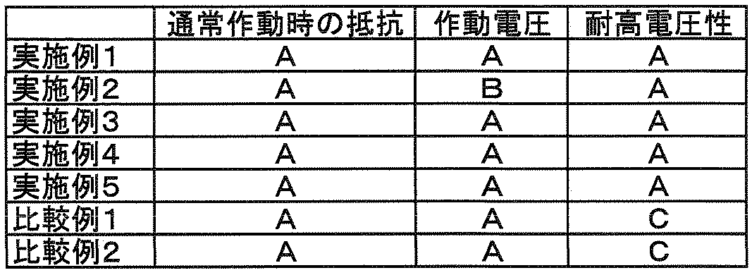
- an electrostatic discharge protector was obtained by the above-described method, and the resistance, operating voltage, and high voltage resistance at normal times were evaluated. The results are shown in Table 1.
- Example 2 To 57 g of paste 1 (solid content: 35% by mass) coated with aluminum particles coated on the surface prepared in Preparation Example 1, 18.2 g of thermosetting urethane resin 1 (solid content: 45% by mass) synthesized in Synthesis Example 1 In addition, 0.63 g of an epoxy resin (manufactured by Japan Epoxy Resin Co., Ltd .: JER604) was added as a curing agent, and the mixture was stirred with a homogenizer at 2000 rpm for 15 minutes to obtain a resin composition for filling a discharge gap.
- an epoxy resin manufactured by Japan Epoxy Resin Co., Ltd .: JER604
- the mass occupancy of the aluminum particles (A) coated on the surface of the obtained resin composition for filling a discharge gap was 70% by mass, and the mass occupancy of the layered material (B) was 0% by mass. .
- an electrostatic discharge protector was obtained by the above-described method, and the resistance, operating voltage, and high voltage resistance at normal times were evaluated. The results are shown in Table 1.
- Example 3 57 g of paste 1 (solid content: 35% by mass) containing aluminum particles coated on the surface prepared in Preparation Example 1 and “UF-G5” (artificial graphite fine powder, scaly, average particle size) as layered substance (B) 1Hg of thermosetting urethane resin 2 (non-volatile content: 52% by mass) synthesized in Synthesis Example 2 was added to 1.0 g of 3 ⁇ m, manufactured by Showa Denko KK, and YH-434 (Toto Kasei Co., Ltd.) was added as a curing agent.
- paste 1 solid content: 35% by mass
- U-G5 artificial graphite fine powder, scaly, average particle size
- Example 4 44 g of the aluminum particle paste 2 coated with the surface prepared in Preparation Example 2 (solid content: 45% by mass), “UF-G5” (artificial graphite fine powder, scaly, average particle diameter of 3 ⁇ m, Showa, Showa)
- U-G5 artificial graphite fine powder, scaly, average particle diameter of 3 ⁇ m, Showa, Showa
- an epoxy resin Japan Epoxy
- Example 5 30 g of the aluminum particle paste 3 (solid content 66% by mass) coated with the surface prepared in Preparation Example 3 and “UF-G5” (artificial graphite fine powder, scaly, average particle diameter 3 ⁇ m, Showa, as a layered substance (B) D. Co., Ltd. (1.0 g) and propylene glycol monomethyl ether (27 g) were added with 18.2 g of thermosetting urethane resin 1 (solid content 45% by mass) synthesized in Synthesis Example 1 and epoxy resin (Japan Epoxy) as a curing agent. Resin Co., Ltd.
- An electrostatic discharge protector having a free shape can be obtained by using a discharge gap filling composition containing metal particles (A) whose surface is coated with a hydrolysis product of a specific metal alkoxide and a binder component (C). Therefore, it is possible to reduce the size and cost of the ESD countermeasure.
- the electrostatic discharge protector can be provided on an electronic circuit board such as a flexible electronic circuit board, and the electronic circuit board can be provided on an electronic device.
- Electrostatic discharge protector 12A ... Electrode 12B ... Electrode 13 ... Discharge gap filling member 14 ... Discharge gap 21 . Electrostatic discharge protector 22A ... Electrode 22B ... Electrode 23 ... .... Discharge gap filling member 24 ... Discharge gap 31 . Electrostatic discharge protector 32A ... Electrode 32B ... Electrode 33 ... Discharge gap filling member 34 ... Discharge gap 35 ... Protective layer
Landscapes
- Engineering & Computer Science (AREA)
- Microelectronics & Electronic Packaging (AREA)
- Physics & Mathematics (AREA)
- Electromagnetism (AREA)
- Manufacturing & Machinery (AREA)
- Compositions Of Macromolecular Compounds (AREA)
- Paints Or Removers (AREA)
- Conductive Materials (AREA)
Abstract
Description
[1]金属粒子を、下記一般式(1)で表される金属アルコキシドの加水分解生成物で被覆してなる金属粒子(A)およびバインダー成分(C)を含むことを特徴とする放電ギャップ充填用組成物。

[2]前記一般式(1)のMの元素が、ケイ素、チタン、ジルコニウム、タンタルまたはハフニウムである[1]に記載の放電ギャップ充填用組成物。
[3]前記金属粒子(A)の金属粒子が、酸化皮膜を有する金属粒子である、[1]または[2]に記載の放電ギャップ充填用組成物。
[4]前記酸化皮膜を有する金属粒子の金属が、マンガン、ニオブ、ジルコニウム、ハフニウム、タンタル、モリブデン、バナジウム、ニッケル、コバルト、クロム、マグネシウム、チタンおよびアルミニウムからなる群から選ばれる少なくとも1つである、[3]に記載の放電ギャップ充填用組成物。
[5]前記金属粒子(A)および前記バインダー成分(C)と共に、さらに層状物質(B)を含むことを特徴とする[1]~[4]のいずれかに記載の放電ギャップ充填用組成物。
[6]前記層状物質(B)が、粘土鉱物結晶(B1)および層状カーボン材料(B2)からなる群から選ばれる少なくとも1つである、[5]に記載の放電ギャップ充填用組成物。
[7]前記層状物質(B)が、層状カーボン材料(B2)である、[5]に記載の放電ギャップ充填用組成物。
[8]前記層状カーボン材料(B2)が、カーボンナノチューブ、気相成長カーボンファイバー、カーボンフラーレン、黒鉛およびカルビン系炭素材料からなる群から選ばれる少なくとも1つである、[7]に記載の放電ギャップ充填用組成物。
[9]前記バインダー成分(C)が、熱硬化性または活性エネルギー線硬化性の化合物を含むことを特徴とする、[1]~[8]のいずれかに記載の放電ギャップ充填用組成物。
[10]前記バインダー成分(C)が、熱硬化性ウレタン樹脂を含むことを特徴とする、[1]~[8]のいずれかに記載の放電ギャップ充填用組成物。
[11] 放電ギャップを形成する2つの電極と前記放電ギャップに充填された放電ギャップ充填部材とを有してなる静電放電保護体であって、前記放電ギャップ充填部材が[1]~[10]のいずれかに記載の放電ギャップ充填用組成物から形成され、前記放電ギャップの距離が5~300μmであることを特徴とする静電放電保護体。
[12]前記放電ギャップ充填部材の表面の全部または一部を覆う保護層を有することを特徴とする、[11]に記載の静電放電保護体。
[13][11]または[12]に記載の静電放電保護体を設けた電子回路基板。
[14]フレキシブル電子回路基板である[13]に記載の電子回路基板。
[15][13]または[14]に記載の電子回路基板を設けた電子機器。
<放電ギャップ充填用組成物>
本発明の放電ギャップ充填用組成物は、金属粒子(A)およびバインダー成分(C)を含有し、必要に応じて層状物質(B)等を含有することができる。
金属粒子(A)
本発明に用いられる金属粒子(A)とは、金属粒子を、下記一般式(1)で表される金属アルコキシドの加水分解生成物で被覆してなる金属粒子である。

層状物質(B)
本発明の組成物は、より良好なESD保護特性を得るという観点から、層状物質(B)を含有することが好ましい。層状物質(B)とは、複数の層がファンデルワールス力で結合して形成されている物質であり、イオン交換などによって、その結晶内の特定の位置に本来その結晶の構成にあずからない原子や分子やイオンを入り込ませることができ、それによって結晶構造が変化しない化合物である。原子や分子やイオンが入り込む位置、すなわちホスト位置は、平面的な層構造をしている。そのような層状物質(B)の典型的なものには、粘土鉱物結晶(B1)やグラファイト(黒鉛)などの層状カーボン材料(B2)あるいは遷移金属のカルコゲン化物などがある。それらの化合物は、ゲストとして金属原子や無機分子、有機分子などを結晶内に取り込むことによってそれぞれ特異な性質を発現する。
バインダー成分(C)
本発明のバインダー成分(C)は、その中に表面が被覆された金属粒子(A)や層状物質(B)を分散させるための絶縁体物質であり、例えば有機系ポリマー、無機系ポリマーおよびそれらの複合ポリマーを挙げることができる。
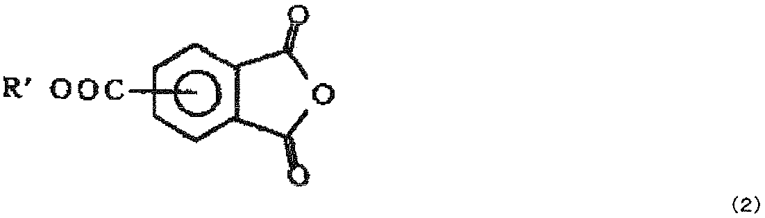
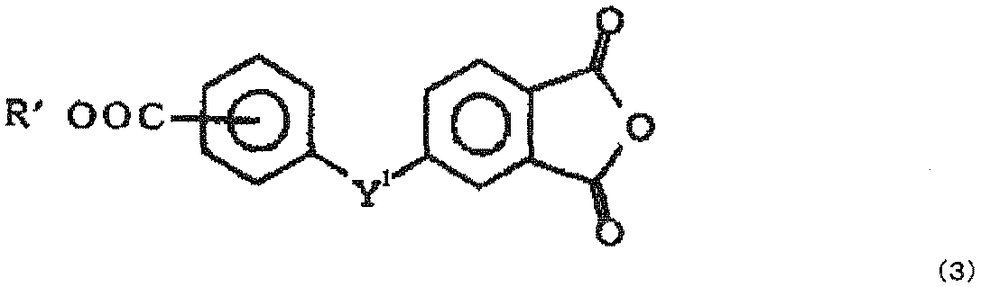
酸無水物基を有する3価のポリカルボン酸およびその誘導体としては、耐熱性、コスト面等から、トリメリット酸無水物が、特に好ましい。
その他の成分
本発明に係る放電ギャップ充填用組成物は、表面が被覆された金属粒子(A)、層状物質(B)およびバインダー成分(C)の他、必要に応じて硬化触媒、硬化促進剤、充填剤、溶剤、発泡剤、消泡剤、レベリング剤、滑剤、可塑剤、抗錆剤、粘度調整剤、着色剤等を含有することができる。また、シリカ粒子などの絶縁性粒子を含有することができる。
放電ギャップ充填用組成物の製造方法
本発明の放電ギャップ充填用組成物を製造するには、例えば、表面が被覆された金属粒子(A)およびバインダー成分(C)の他、必要に応じて層状物質(B)、さらに必要に応じてその他の成分である溶剤、充填剤、硬化触媒などを、ディスパー、ニーダー、3本ロールミル、ビーズミル、自転公転型撹拌機などを用いて分散、混合する。混合の際は、相溶性を良好にするために十分な温度に加温してもよい。上記の分散、混合ののち、必要に応じてさらに硬化促進剤を加えて混合して、調製することができる。
<静電放電保護体>
本発明の静電放電保護体は、静電放電時にデバイスを保護するため、過電流をアースに逃すための保護回路として用いられる。本発明の静電放電保護体は、通常作動時の低い電圧のときには、高い電気抵抗値を示し、電流をアースに逃がさずデバイスに供給する。一方、静電放電が生じたときには、即座に低い電気抵抗値を示し、過電流をアースに逃し、過電流がデバイスに供給されるのを阻止する。静電放電の過渡現象が解消したときには、高い電気抵抗値に戻り、電流をデバイスに供給する。本発明の静電放電保護体は、放電ギャップに、絶縁性のバインダー成分(C)を含む前記放電ギャップ充填用組成物から形成された放電ギャップ充填部材が充填されているため、通常作動時に漏れ電流は発生しない。例えば、電極間にDC10V以下の電圧を印加した場合の抵抗値を1010Ω以上にすることが可能となり、静電放電保護を実現することができる。
<静電放電保護体の作製>
膜厚25μmのポリイミドフィルム上に一対の電極パターン(膜厚12μm、放電ギャップの距離50μm、電極幅500μm)を形成した配線基板に、後述する方法で得られた放電ギャップ充填用組成物を、針先が直径2mmで平坦なニードルを用いて塗布し、電極パターンを覆うように放電ギャップに充填した後、120℃恒温器内で60分保持して放電ギャップ充填部材を形成させた。その後、シリコーン樹脂(X14-B2334:モメンティブ社製)を前述の静電保護体を完全に覆うように塗布しすぐに120℃の硬化炉に入れて、120℃で1時間硬化して保護膜を形成し、静電放電保護体を得た。
<通常作動電圧時の絶縁性の評価方法>
静電放電保護体の両端の電極部について、絶縁抵抗計「MEGOHMMETER SM-8220」を用いて、DC10V印加における抵抗を「通常作動時の抵抗」として測定した。
B :電気抵抗値が1010Ω未満を示す
<作動電圧の評価方法>
半導体用静電気試験器ESS-6008(NOISE LABORATORY社製)を用いて、任意の印加電圧のPeak電流を測定した後、得られた静電放電保護体をとりつけて同じ印加電圧を与え、Peak電流を測定したとき、静電放電保護体がない場合のPeak電流の70%以上の電流が観測された場合、その印加電圧を「作動電圧」として評価した。
B :作動電圧 1000V以上 2000V未満
C :作動電圧 2000V以上
<耐高電圧性の評価方法>
得られた静電放電保護体を半導体用静電気試験器ESS-6008(NOISE LABORATORY社製)にとりつけ、8kVの印加電圧を10回与えた後、絶縁抵抗計MEGOHMMETER SM-8220を用いて、DC10V印加における抵抗値を測定した。これを、「耐高電圧性」として評価した。
B : 108Ω以上、1010Ω未満
C : 108Ω未満
<表面が被覆された金属粒子(A)の調製例1>表面が被覆されたAl粒子を含むペースト1
東洋アルミパウダー社製の酸化皮膜を有する球状アルミ粒子(商品名:08-0076、平均粒径:2.5μm)49gをプロピレングリコールモノメチルエーテル724gに分散させ、この分散液にイオン交換水169gおよび25質量%アンモニア水32gを添加して攪拌し、アルミパウダースラリーを得、この液温を30℃に保持した。次にテトラエトキシシラン13.2gをプロピレングリコールモノメチルエーテル13.2gで希釈し、この液を12時間かけて、一定速度で上記アルミパウダースラリーに滴下し、成膜テトラエトキシシランの加水分解の進行に伴って、テトラエトキシシランの加水分解生成物によるアルミ粒子の表面被覆を行った。
<表面が被覆された金属粒子(A)の調製例2>表面が被覆されたAl粒子を含むペースト2
東洋アルミパウダー社製の酸化皮膜を有する球状アルミ粒子(商品名:08-0076、平均粒径:2.5μm)49gをプロピレングリコールモノメチルエーテル724gに分散させ、この分散液にイオン交換水169gおよび25質量%アンモニア水32gを添加して攪拌し、アルミパウダースラリーを得、この液温を30℃に保持した。次にテトラ-n-ブチルチタネート 21.6gをプロピレングリコールモノメチルエーテル21.6gで希釈し、この液を12時間かけて、一定速度で上記アルミパウダースラリーに滴下し、テトラ-n-ブチルチタネートの加水分解の進行に伴って、テトラ-n-ブチルチタネートの加水分解生成物によるアルミ粒子の表面被覆を行った。
<表面が被覆された金属粒子(A)の調製例3>表面が被覆されたAl粒子を含むペースト3
東洋アルミパウダー社製の酸化皮膜を有する球状アルミ粒子(商品名:08-0076、平均粒径:2.5μm)49gをプロピレングリコールモノメチルエーテル724gに分散させ、この分散液にイオン交換水169gおよび25質量%アンモニア水32gを添加して攪拌し、アルミパウダースラリーを得、この液温を30℃に保持した。次にテトラ-n-ブチルジルコネート 27.0gをプロピレングリコールモノメチルエーテル27.0gで希釈し、この液を12時間かけて、一定速度で上記アルミパウダースラリーに滴下し、テトラ-n-ブチルジルコネートの加水分解の進行に伴って、テトラ-n-ブチルジルコネートの加水分解生成物によるアルミ粒子の表面被覆を行った。
<バインダー成分(C)の合成例1>熱硬化性ウレタン樹脂1
攪拌装置、温度計、コンデンサーを備えた反応容器に、ポリカーボネートジオールとしてC-1015N(株式会社クラレ製ポリカーボネートジオール、原料ジオールモル比:1,9-ノナンジオール:2-メチル-1,8-オクタンジオール=15:85、分子量964)718.2g、カルボキシル基を有するジヒドロキシル化合物として2,2-ジメチロールブタン酸(日本化成株式会社製)136.6g、溶媒としてジエチレングリコールエチルエーテルアセテート(ダイセル化学株式会社製)1293gを仕込み、90℃ですべての原料を溶解した。反応液の温度を70℃まで下げ、滴下ロートにより、ポリイソシアネートとしてメチレンビス(4-シクロヘキシルイソシアネート)(住化バイエルウレタン(株)製、商品名「デスモジュール-W」)237.5gを30分かけて滴下した。滴下終了後、80℃で1時間、90℃で1時間、100℃で1.5時間反応を行い、ほぼイソシアネートが消失したことを確認した後、イソブタノール(和光純薬株式会社製)2.13gを滴下し、更に105℃にて1時間反応を行った。得られたカルボキシル基含有ウレタンの数平均分子量は6090、固形分酸価は40.0mgKOH/gであった。これを固形分45質量%になるようにγ―ブチロラクトンを加えて希釈した。
<バインダー成分(C)の合成例2>熱硬化性ウレタン樹脂2
実施例1と同様の攪拌機、油水分離器付き冷却管、窒素導入管および温度計を備えた5リットルの四つ口フラスコに、PLACCEL CD-220(ダイセル化学(株)製1,6-ヘキサンジオール系ポリカーボネートジオールの商品名)1000.0g(0.50モル)および4,4′-ジフェニルメタンジイソシアネート250.27g(1.00モル)と、γ-ブチロラクトン833.51gを仕込み、140℃まで昇温した。140℃で5時間反応させ、第2のジイソシアネートを得た。更に、この反応液に無水物基を有するポリカルボン酸として無水トリメリット酸288.20g(1.50モル)、さらに4,4′-ジフェニルメタンジイソシアネート125.14g(0.50モル)およびγ-ブチロラクトン1361.14gを仕込み、160℃まで昇温した後、6時間反応させて、数平均分子量が18,000の樹脂を得た。得られた樹脂をγ-ブチロラクトンで希釈し、粘度160Pa・s、不揮発分52重量%のポリアミドイミド樹脂溶液、つまり酸無水物基含有熱硬化性ウレタン樹脂の溶液を得た。
[実施例1]
調製例1で調製した表面が被覆されたアルミ粒子を含むペースト1(固形分35質量%)57g、および層状物質(B)として「UF-G5」(人造黒鉛微粉末、鱗片状、平均粒子径3μm、昭和電工株式会社製)1.0gに、合成例1で合成した熱硬化性ウレタン樹脂1(固形分45質量%)18.2gを加え、硬化剤としてエポキシ樹脂(ジャパンエポキシレジン社製:JER604)0.63gを加えて、ホモジナイザーにて2000rpmで15分間攪拌し、放電ギャップ充填用樹脂組成物を得た。得られた放電ギャップ充填用樹脂組成物に占める表面が被覆されたアルミ粒子(A)の質量占有率は、67質量%で、層状物質(B)の質量占有率は、3質量%であった。この放電ギャップ用樹脂組成物を用いて上記方法により静電放電保護体を得て、通常時の抵抗、作動電圧、耐高電圧性を評価した。結果を表1に示す。
[実施例2]
調製例1で調製した表面が被覆されたアルミ粒子を含むペースト1(固形分35質量%)57gに、合成例1で合成した熱硬化性ウレタン樹脂1(固形分45質量%)18.2gを加え、硬化剤としてエポキシ樹脂(ジャパンエポキシレジン社製:JER604)0.63gを加えて、ホモジナイザーにて2000rpmで15分間攪拌し、放電ギャップ充填用樹脂組成物を得た。得られた放電ギャップ充填用樹脂組成物に占める表面が被覆されたアルミ粒子(A)の質量占有率は、70質量%で、層状物質(B)の質量占有率は、0質量%であった。この放電ギャップ用樹脂組成物を用いて上記方法により静電放電保護体を得て、通常時の抵抗、作動電圧、耐高電圧性を評価した。結果を表1に示す。
[実施例3]
調製例1で調製した表面が被覆されたアルミ粒子を含むペースト1(固形分 35質量%)57g、および層状物質(B)として「UF-G5」(人造黒鉛微粉末、鱗片状、平均粒子径3μm、昭和電工株式会社製)1.0gに、合成例2で合成した熱硬化性ウレタン樹脂2(不揮発分52質量%)15.8gを加え、硬化剤として、YH-434(東都化成(株)製アミン型エポキシ樹脂の商品名、エポキシ当量約120、エポキシ基4個/分子)1.58gを加えて、ホモジナイザーにて2000rpmで15分間攪拌し、放電ギャップ充填用樹脂組成物を得た。得られた放電ギャップ充填用樹脂組成物に占める表面が被覆されたアルミ粒子(A)の質量占有率は、65質量%で、層状物質(B)の質量占有率は、3質量%であった。この放電ギャップ用樹脂組成物を用いて上記方法により静電放電保護体を得て、通常時の抵抗、作動電圧、耐高電圧性を評価した。結果を表1に示す。
[実施例4]
調製例2で調製した表面が被覆されたアルミ粒子ペースト2(固形分 45質量%)44g、層状物質(B)として「UF-G5」(人造黒鉛微粉末、鱗片状、平均粒子径3μm、昭和電工株式会社製)1.0g、およびプロピレングリコールモノメチルエーテル 13gに、合成例1で合成した熱硬化性ウレタン樹脂1(固形分45質量%)18.2gを加え、硬化剤としてエポキシ樹脂(ジャパンエポキシレジン社製:JER604)0.63gを加えて、ホモジナイザーにて2000rpmで15分間攪拌し、放電ギャップ充填用樹脂組成物を得た。得られた放電ギャップ充填用樹脂組成物に占める表面が被覆されたアルミ粒子(A)の質量占有率は、67質量%で、層状物質(B)の質量占有率は、3質量%であった。この放電ギャップ用樹脂組成物を用いて上記方法により静電放電保護体を得て、通常時の抵抗、作動電圧、耐高電圧性を評価した。結果を表1に示す。
[実施例5]
調製例3で調製した表面が被覆されたアルミ粒子ペースト3(固形分 66質量%)30g、層状物質(B)として「UF-G5」(人造黒鉛微粉末、鱗片状、平均粒子径3μm、昭和電工株式会社製)1.0g、およびプロピレングリコールモノメチルエーテル 27gに、合成例1で合成した熱硬化性ウレタン樹脂1(固形分45質量%)18.2gを加え、硬化剤としてエポキシ樹脂(ジャパンエポキシレジン社製:JER604)0.63gを加えて、ホモジナイザーにて2000rpmで15分間攪拌し、放電ギャップ充填用樹脂組成物を得た。得られた放電ギャップ充填用樹脂組成物に占める表面が被覆されたアルミ粒子(A)の質量占有率は、67質量%で、層状物質(B)の質量占有率は、3質量%であった。この放電ギャップ用樹脂組成物を用いて上記方法により静電放電保護体を得て、通常時の抵抗、作動電圧、耐高電圧性を評価した。結果を表1に示す。
[比較例1]
調製例1で調製した表面が被覆されたアルミ粒子ペースト1 57gの替わりに、東洋アルミパウダー社製の酸化皮膜を有する球状アルミ粒子08-0076(平均粒径 2.5μm)20gを使用した以外は、実施例1と同様な方法で放電ギャップ充填用樹脂組成物を得た。得られた放電ギャップ充填用樹脂組成物に占める表面が被覆されていないアルミ粒子の質量占有率は、67質量%で、層状物質(B)の質量占有率は、3質量%であった。
[比較例2]
調製例1で調製した表面が被覆されたアルミ粒子ペースト1 57gの替わりに、東洋アルミパウダー社製の酸化皮膜を有する球状アルミ粒子08-0076(平均粒径 2.5μm)20gおよび、ヒュームドシリカ(Cabot社製 Cabosil M-5)0.76gを使用した以外は、実施例1と同様な方法で放電ギャップ充填用樹脂組成物を得た。得られた放電ギャップ充填用樹脂組成物に占める球状アルミ粒子08-0076およびヒュームドシリカの質量占有率は、67質量%で、層状物質(B)の質量占有率は、3質量%であった。
12A・・電極
12B・・電極
13・・・放電ギャップ充填部材
14・・・放電ギャップ
21・・・静電放電保護体
22A・・電極
22B・・電極
23・・・放電ギャップ充填部材
24・・・放電ギャップ
31・・・静電放電保護体
32A・・電極
32B・・電極
33・・・放電ギャップ充填部材
34・・・放電ギャップ
35・・・保護層
Claims (15)
- 金属粒子を、下記一般式(1)で表される金属アルコキシドの加水分解生成物で被覆してなる金属粒子(A)およびバインダー成分(C)を含むことを特徴とする放電ギャップ充填用組成物。

- 前記一般式(1)のMの元素が、ケイ素、チタン、ジルコニウム、タンタルまたはハフニウムである請求項1に記載の放電ギャップ充填用組成物。
- 前記金属粒子(A)の金属粒子が、酸化皮膜を有する金属粒子である、請求項1または2に記載の放電ギャップ充填用組成物。
- 前記酸化皮膜を有する金属粒子の金属が、マンガン、ニオブ、ジルコニウム、ハフニウム、タンタル、モリブデン、バナジウム、ニッケル、コバルト、クロム、マグネシウム、チタンおよびアルミニウムからなる群から選ばれる少なくとも1つである、請求項3に記載の放電ギャップ充填用組成物。
- 前記金属粒子(A)および前記バインダー成分(C)と共に、さらに層状物質(B)を含むことを特徴とする請求項1~4のいずれかに記載の放電ギャップ充填用組成物。
- 前記層状物質(B)が、粘土鉱物結晶(B1)および層状カーボン材料(B2)からなる群から選ばれる少なくとも1つである、請求項5に記載の放電ギャップ充填用組成物。
- 前記層状物質(B)が、層状カーボン材料(B2)である、請求項5に記載の放電ギャップ充填用組成物。
- 前記層状カーボン材料(B2)が、カーボンナノチューブ、気相成長カーボンファイバー、カーボンフラーレン、黒鉛およびカルビン系炭素材料からなる群から選ばれる少なくとも1つである、請求項7に記載の放電ギャップ充填用組成物。
- 前記バインダー成分(C)が、熱硬化性または活性エネルギー線硬化性の化合物を含むことを特徴とする、請求項1~8のいずれかに記載の放電ギャップ充填用組成物。
- 前記バインダー成分(C)が、熱硬化性ウレタン樹脂を含むことを特徴とする、請求項1~8のいずれかに記載の放電ギャップ充填用組成物。
- 放電ギャップを形成する2つの電極と前記放電ギャップに充填された放電ギャップ充填部材とを有してなる静電放電保護体であって、前記放電ギャップ充填部材が請求項1~10のいずれかに記載の放電ギャップ充填用組成物から形成され、前記放電ギャップの距離が5~300μmであることを特徴とする静電放電保護体。
- 前記放電ギャップ充填部材の表面の全部または一部を覆う保護層を有することを特徴とする、請求項11に記載の静電放電保護体。
- 請求項11または12に記載の静電放電保護体を設けた電子回路基板。
- フレキシブル電子回路基板である請求項13に記載の電子回路基板。
- 請求項13または14に記載の電子回路基板を設けた電子機器。
Priority Applications (5)
| Application Number | Priority Date | Filing Date | Title |
|---|---|---|---|
| US13/257,144 US20120006583A1 (en) | 2009-03-19 | 2010-03-17 | Discharge gap filling composition and electrostatic discharge protector |
| KR1020117024362A KR101276985B1 (ko) | 2009-03-19 | 2010-03-17 | 방전 갭 충전용 조성물 및 정전 방전 보호체 |
| CN2010800122738A CN102356526B (zh) | 2009-03-19 | 2010-03-17 | 放电间隙填充用组合物和静电放电保护体 |
| JP2011504864A JP5400134B2 (ja) | 2009-03-19 | 2010-03-17 | 放電ギャップ充填用組成物および静電放電保護体 |
| US14/513,895 US20150062763A1 (en) | 2009-03-19 | 2014-10-14 | Discharge gap filling composition and electrostatic discharge protector |
Applications Claiming Priority (2)
| Application Number | Priority Date | Filing Date | Title |
|---|---|---|---|
| JP2009-067332 | 2009-03-19 | ||
| JP2009067332 | 2009-03-19 |
Related Child Applications (2)
| Application Number | Title | Priority Date | Filing Date |
|---|---|---|---|
| US13/257,144 A-371-Of-International US20120006583A1 (en) | 2009-03-19 | 2010-03-17 | Discharge gap filling composition and electrostatic discharge protector |
| US14/513,895 Division US20150062763A1 (en) | 2009-03-19 | 2014-10-14 | Discharge gap filling composition and electrostatic discharge protector |
Publications (1)
| Publication Number | Publication Date |
|---|---|
| WO2010107059A1 true WO2010107059A1 (ja) | 2010-09-23 |
Family
ID=42739719
Family Applications (1)
| Application Number | Title | Priority Date | Filing Date |
|---|---|---|---|
| PCT/JP2010/054546 Ceased WO2010107059A1 (ja) | 2009-03-19 | 2010-03-17 | 放電ギャップ充填用組成物および静電放電保護体 |
Country Status (6)
| Country | Link |
|---|---|
| US (2) | US20120006583A1 (ja) |
| JP (1) | JP5400134B2 (ja) |
| KR (1) | KR101276985B1 (ja) |
| CN (1) | CN102356526B (ja) |
| TW (1) | TWI477542B (ja) |
| WO (1) | WO2010107059A1 (ja) |
Cited By (2)
| Publication number | Priority date | Publication date | Assignee | Title |
|---|---|---|---|---|
| WO2012105515A1 (ja) * | 2011-02-02 | 2012-08-09 | 昭和電工株式会社 | 放電ギャップ充填用組成物および静電放電保護体 |
| JP2017092441A (ja) * | 2015-11-16 | 2017-05-25 | サムソン エレクトロ−メカニックス カンパニーリミテッド. | 静電気放電保護用組成物及びその組成物を用いた静電気放電保護素子 |
Families Citing this family (10)
| Publication number | Priority date | Publication date | Assignee | Title |
|---|---|---|---|---|
| WO2013132988A1 (ja) * | 2012-03-05 | 2013-09-12 | 昭和電工株式会社 | 放電ギャップ充填用組成物および静電放電保護体 |
| DE102012208730A1 (de) | 2012-05-24 | 2013-11-28 | Osram Opto Semiconductors Gmbh | Optoelektronische Bauelementevorrichtung und Verfahren zum Herstellen einer optoelektronischen Bauelementevorrichtung |
| EP2682941A1 (de) * | 2012-07-02 | 2014-01-08 | Technische Universität Ilmenau | Vorrichtung, Verfahren und Computerprogramm für frei wählbare Frequenzverschiebungen in der Subband-Domäne |
| JP5784688B2 (ja) * | 2012-12-10 | 2015-09-24 | サムソン エレクトロ−メカニックス カンパニーリミテッド. | 静電気放電構造及び静電気放電構造の製造方法 |
| KR20170109782A (ko) | 2016-03-22 | 2017-10-10 | 삼성전기주식회사 | 복합 전자 부품 |
| JP6661445B2 (ja) * | 2016-03-31 | 2020-03-11 | 国立大学法人 東京大学 | 高周波アンテナ素子、及び高周波アンテナモジュール |
| DE102017214287A1 (de) * | 2017-08-16 | 2019-02-21 | Siemens Aktiengesellschaft | Überspannungsableiter und Herstellungsverfahren für einen Überspannungsableiter |
| KR101985499B1 (ko) * | 2017-12-28 | 2019-06-03 | 삼화콘덴서공업 주식회사 | 과전류 보호 기능을 가지는 금속 산화물 바리스터 |
| KR20210080746A (ko) * | 2019-12-23 | 2021-07-01 | 삼성전기주식회사 | 저항 부품 |
| EP3926647A3 (en) | 2020-06-15 | 2022-03-16 | Littelfuse, Inc. | A method for thin-film coating packaging of device having meltable and wetting links |
Citations (3)
| Publication number | Priority date | Publication date | Assignee | Title |
|---|---|---|---|---|
| JPH0574609A (ja) * | 1991-09-13 | 1993-03-26 | Toshiba Corp | 酸化物抵抗体の製造方法 |
| WO2006085492A1 (ja) * | 2005-02-09 | 2006-08-17 | Matsushita Electric Industrial Co., Ltd. | 静電気保護機能付きチップ部品 |
| WO2008155916A1 (ja) * | 2007-06-21 | 2008-12-24 | Panasonic Corporation | 静電気対策部品およびその製造方法 |
Family Cites Families (13)
| Publication number | Priority date | Publication date | Assignee | Title |
|---|---|---|---|---|
| JP2622999B2 (ja) * | 1988-01-27 | 1997-06-25 | 日本油脂 株式会社 | 有彩色金属フレーク顔料並びにこの顔料を含有する塗料組成物、インキ組成物、化粧料組成物及びプラスチック成形組成物 |
| JP3807086B2 (ja) * | 1998-03-23 | 2006-08-09 | 味の素株式会社 | 粒度分布制御晶析法 |
| JP3389240B2 (ja) * | 1999-12-21 | 2003-03-24 | 松下電器産業株式会社 | プラズマディスプレイパネルおよびその製造方法 |
| US7034652B2 (en) * | 2001-07-10 | 2006-04-25 | Littlefuse, Inc. | Electrostatic discharge multifunction resistor |
| US6740469B2 (en) * | 2002-06-25 | 2004-05-25 | Brewer Science Inc. | Developer-soluble metal alkoxide coatings for microelectronic applications |
| JP2004124069A (ja) * | 2002-07-31 | 2004-04-22 | Showa Denko Kk | シリカ被覆アルミニウム顔料およびその製造方法並びにその用途 |
| US7300967B2 (en) * | 2004-11-12 | 2007-11-27 | Eastman Chemical Company | Polyester polymer and copolymer compositions containing metallic titanium particles |
| KR20060078556A (ko) * | 2004-12-31 | 2006-07-05 | 주식회사 케이씨씨 | 자외선 경화형 도료 조성물 |
| JP5265854B2 (ja) * | 2005-12-08 | 2013-08-14 | 昭和電工株式会社 | 熱硬化性樹脂組成物、熱可塑性樹脂溶液および皮膜形成材料ならびにこれらの硬化物 |
| CN101003725A (zh) * | 2006-01-21 | 2007-07-25 | 富准精密工业(深圳)有限公司 | 热界面材料及其制作方法 |
| US8206614B2 (en) * | 2008-01-18 | 2012-06-26 | Shocking Technologies, Inc. | Voltage switchable dielectric material having bonded particle constituents |
| WO2010147095A1 (ja) * | 2009-06-17 | 2010-12-23 | 昭和電工株式会社 | 放電ギャップ充填用組成物および静電放電保護体 |
| CN103329369B (zh) * | 2011-02-02 | 2015-09-02 | 昭和电工株式会社 | 放电间隙填充用组合物和静电放电保护体 |
-
2010
- 2010-03-17 KR KR1020117024362A patent/KR101276985B1/ko not_active Expired - Fee Related
- 2010-03-17 CN CN2010800122738A patent/CN102356526B/zh not_active Expired - Fee Related
- 2010-03-17 JP JP2011504864A patent/JP5400134B2/ja not_active Expired - Fee Related
- 2010-03-17 WO PCT/JP2010/054546 patent/WO2010107059A1/ja not_active Ceased
- 2010-03-17 US US13/257,144 patent/US20120006583A1/en not_active Abandoned
- 2010-03-19 TW TW099108182A patent/TWI477542B/zh not_active IP Right Cessation
-
2014
- 2014-10-14 US US14/513,895 patent/US20150062763A1/en not_active Abandoned
Patent Citations (3)
| Publication number | Priority date | Publication date | Assignee | Title |
|---|---|---|---|---|
| JPH0574609A (ja) * | 1991-09-13 | 1993-03-26 | Toshiba Corp | 酸化物抵抗体の製造方法 |
| WO2006085492A1 (ja) * | 2005-02-09 | 2006-08-17 | Matsushita Electric Industrial Co., Ltd. | 静電気保護機能付きチップ部品 |
| WO2008155916A1 (ja) * | 2007-06-21 | 2008-12-24 | Panasonic Corporation | 静電気対策部品およびその製造方法 |
Cited By (7)
| Publication number | Priority date | Publication date | Assignee | Title |
|---|---|---|---|---|
| WO2012105515A1 (ja) * | 2011-02-02 | 2012-08-09 | 昭和電工株式会社 | 放電ギャップ充填用組成物および静電放電保護体 |
| CN103329369A (zh) * | 2011-02-02 | 2013-09-25 | 昭和电工株式会社 | 放电间隙填充用组合物和静电放电保护体 |
| EP2672586A4 (en) * | 2011-02-02 | 2015-01-14 | Showa Denko Kk | COMPOSITION FOR FILLING A DISCHARGE COLUMN AND ELECTROSTATIC DISCHARGE PROTECTION |
| CN103329369B (zh) * | 2011-02-02 | 2015-09-02 | 昭和电工株式会社 | 放电间隙填充用组合物和静电放电保护体 |
| KR101568917B1 (ko) * | 2011-02-02 | 2015-11-12 | 쇼와 덴코 가부시키가이샤 | 방전 갭 충전용 조성물 및 정전 방전 보호체 |
| JP5819327B2 (ja) * | 2011-02-02 | 2015-11-24 | 昭和電工株式会社 | 放電ギャップ充填用組成物および静電放電保護体および電子回路基板 |
| JP2017092441A (ja) * | 2015-11-16 | 2017-05-25 | サムソン エレクトロ−メカニックス カンパニーリミテッド. | 静電気放電保護用組成物及びその組成物を用いた静電気放電保護素子 |
Also Published As
| Publication number | Publication date |
|---|---|
| CN102356526B (zh) | 2013-08-28 |
| US20150062763A1 (en) | 2015-03-05 |
| KR101276985B1 (ko) | 2013-06-24 |
| JPWO2010107059A1 (ja) | 2012-09-20 |
| KR20110138383A (ko) | 2011-12-27 |
| US20120006583A1 (en) | 2012-01-12 |
| JP5400134B2 (ja) | 2014-01-29 |
| CN102356526A (zh) | 2012-02-15 |
| TW201105719A (en) | 2011-02-16 |
| TWI477542B (zh) | 2015-03-21 |
Similar Documents
| Publication | Publication Date | Title |
|---|---|---|
| JP5400134B2 (ja) | 放電ギャップ充填用組成物および静電放電保護体 | |
| JP5551696B2 (ja) | 放電ギャップ充填用組成物および静電放電保護体 | |
| JP5819327B2 (ja) | 放電ギャップ充填用組成物および静電放電保護体および電子回路基板 | |
| JP5314696B2 (ja) | 静電放電保護体 | |
| WO2010101103A1 (ja) | 放電ギャップ充填用組成物および静電放電保護体 | |
| WO2013132988A1 (ja) | 放電ギャップ充填用組成物および静電放電保護体 | |
| JP2014182987A (ja) | 放電ギャップ充填用組成物および静電放電保護体 | |
| JP2013161532A (ja) | 放電ギャップ充填用組成物の製造方法 | |
| JP2014182988A (ja) | 放電ギャップ充填用組成物および静電放電保護体 |
Legal Events
| Date | Code | Title | Description |
|---|---|---|---|
| WWE | Wipo information: entry into national phase |
Ref document number: 201080012273.8 Country of ref document: CN |
|
| 121 | Ep: the epo has been informed by wipo that ep was designated in this application |
Ref document number: 10753551 Country of ref document: EP Kind code of ref document: A1 |
|
| WWE | Wipo information: entry into national phase |
Ref document number: 2011504864 Country of ref document: JP |
|
| WWE | Wipo information: entry into national phase |
Ref document number: 13257144 Country of ref document: US |
|
| NENP | Non-entry into the national phase |
Ref country code: DE |
|
| ENP | Entry into the national phase |
Ref document number: 20117024362 Country of ref document: KR Kind code of ref document: A |
|
| 122 | Ep: pct application non-entry in european phase |
Ref document number: 10753551 Country of ref document: EP Kind code of ref document: A1 |