WO2010106596A1 - 検査方法および検査装置 - Google Patents
検査方法および検査装置 Download PDFInfo
- Publication number
- WO2010106596A1 WO2010106596A1 PCT/JP2009/006212 JP2009006212W WO2010106596A1 WO 2010106596 A1 WO2010106596 A1 WO 2010106596A1 JP 2009006212 W JP2009006212 W JP 2009006212W WO 2010106596 A1 WO2010106596 A1 WO 2010106596A1
- Authority
- WO
- WIPO (PCT)
- Prior art keywords
- detectors
- inspection
- signal
- signal processing
- processing
- Prior art date
- Legal status (The legal status is an assumption and is not a legal conclusion. Google has not performed a legal analysis and makes no representation as to the accuracy of the status listed.)
- Ceased
Links
Images





Classifications
-
- G—PHYSICS
- G01—MEASURING; TESTING
- G01N—INVESTIGATING OR ANALYSING MATERIALS BY DETERMINING THEIR CHEMICAL OR PHYSICAL PROPERTIES
- G01N21/00—Investigating or analysing materials by the use of optical means, i.e. using sub-millimetre waves, infrared, visible or ultraviolet light
- G01N21/84—Systems specially adapted for particular applications
- G01N21/88—Investigating the presence of flaws or contamination
- G01N21/94—Investigating contamination, e.g. dust
-
- G—PHYSICS
- G01—MEASURING; TESTING
- G01N—INVESTIGATING OR ANALYSING MATERIALS BY DETERMINING THEIR CHEMICAL OR PHYSICAL PROPERTIES
- G01N21/00—Investigating or analysing materials by the use of optical means, i.e. using sub-millimetre waves, infrared, visible or ultraviolet light
- G01N21/84—Systems specially adapted for particular applications
- G01N21/88—Investigating the presence of flaws or contamination
- G01N21/95—Investigating the presence of flaws or contamination characterised by the material or shape of the object to be examined
- G01N21/9501—Semiconductor wafers
-
- G—PHYSICS
- G01—MEASURING; TESTING
- G01N—INVESTIGATING OR ANALYSING MATERIALS BY DETERMINING THEIR CHEMICAL OR PHYSICAL PROPERTIES
- G01N21/00—Investigating or analysing materials by the use of optical means, i.e. using sub-millimetre waves, infrared, visible or ultraviolet light
- G01N21/84—Systems specially adapted for particular applications
- G01N21/88—Investigating the presence of flaws or contamination
- G01N21/95—Investigating the presence of flaws or contamination characterised by the material or shape of the object to be examined
- G01N21/956—Inspecting patterns on the surface of objects
-
- G—PHYSICS
- G01—MEASURING; TESTING
- G01N—INVESTIGATING OR ANALYSING MATERIALS BY DETERMINING THEIR CHEMICAL OR PHYSICAL PROPERTIES
- G01N21/00—Investigating or analysing materials by the use of optical means, i.e. using sub-millimetre waves, infrared, visible or ultraviolet light
- G01N21/17—Systems in which incident light is modified in accordance with the properties of the material investigated
- G01N21/47—Scattering, i.e. diffuse reflection
- G01N2021/4704—Angular selective
- G01N2021/4711—Multiangle measurement
-
- G—PHYSICS
- G01—MEASURING; TESTING
- G01N—INVESTIGATING OR ANALYSING MATERIALS BY DETERMINING THEIR CHEMICAL OR PHYSICAL PROPERTIES
- G01N21/00—Investigating or analysing materials by the use of optical means, i.e. using sub-millimetre waves, infrared, visible or ultraviolet light
- G01N21/17—Systems in which incident light is modified in accordance with the properties of the material investigated
- G01N21/47—Scattering, i.e. diffuse reflection
Definitions
- the present invention relates to an inspection technique for an optical inspection apparatus.
- the present invention relates to an inspection method for inspecting foreign matter or defects on the surface of a semiconductor wafer in a semiconductor device manufacturing process, an inspection device for inspecting foreign matter or defects, and a semiconductor device inspection method and inspection device.
- the present invention also relates to an inspection method and an inspection apparatus for DISK and glass substrates other than wafers.
- the inspection threshold is set according to the magnitude of scattered light from the object to be inspected, but generally the same value is set on the entire surface of the object to be inspected.
- a common threshold is used in a plurality of detectors.
- Patent Literature 1 and Patent Literature 2 can be cited as related to these.
- the actual condition of the surface of the object to be inspected is not uniform, and with a uniform inspection threshold on the entire surface of the object to be inspected, the detection sensitivity of the area with the least noise is reduced due to the restriction of the area with the largest noise. There are challenges.
- An object of the present invention is to provide an inspection method or an inspection apparatus that can cope with a change in the surface state of an object to be inspected and can improve detection sensitivity.
- an illumination system that irradiates an inspection object with illumination light, a detection unit that detects scattered light from the inspection object, a plurality of spatially independent detectors, and the plurality of The inspection apparatus includes a signal processing unit that processes each output signal of the detector under independent processing conditions.
- Another feature of the present invention is an inspection method for irradiating an inspection object with illumination light to detect scattered light from the inspection object with a plurality of spatially independent detectors.
- each output signal of the detector is signal-processed under independent processing conditions.
- an inspection apparatus that can cope with a change in the surface state of an object to be inspected and can improve detection sensitivity.
- Another aspect of the present invention is to provide an inspection method that can cope with a change in the surface state of an object to be inspected and can improve detection sensitivity.
- Example of this invention it is explanatory drawing which shows an example of optical system structure in case of four detectors, and distribution of the reflected / scattered light from a sample.
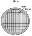
- it is explanatory drawing which shows an example of the area
- It is explanatory drawing which shows the example of another wafer with a pattern in the Example of this invention.
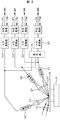
- FIG. 1 shows an example of the configuration of a surface inspection apparatus that is an embodiment of the present invention.
- the light emitted from the light source 1 passes through the light amount adjustment mechanism 2 that can adjust the brightness, the optical axis correction mechanism 3, and the zoom mechanism 5, and is applied to the sample 8 that is an object to be inspected.
- the light emitted from the zoom mechanism 5 is switched to the vertical optical path or the oblique optical path by the vertical oblique irradiation switching mirror 6a.
- the vertically branched light is condensed by the condensing lens 7a and irradiated on the sample 8.
- the sample 8 is mounted on the XYZ ⁇ stage 9.
- the XYZ ⁇ stage is configured to be movable in the respective axial directions of an X axis and a Y axis parallel to the sample surface, a Z axis perpendicular to the sample surface, and a ⁇ axis that enables the sample to rotate.
- it is used for focus adjustment to image the irradiated light by movement in the Z-axis direction, and on the sample surface during surface inspection scanning by movement between the ⁇ -axis direction and the X-axis or Y-axis direction.
- the spot of irradiated light moves spirally from the center of an object to be inspected, such as a wafer, or from the periphery to the center.
- the spot of light irradiated on the sample surface moves from the center of the object to be inspected, such as a wafer, to the outer periphery, or from the outer periphery to the center. Move concentrically. Reflected / scattered light from the sample 8 by the irradiated light is guided to the detector 11 by the detection lens 10. Thereafter, the detected light signal is digitally encoded by the A / D converter 12.
- the foreign matter / defect determination mechanism 13 is connected to an input unit 131 such as a keyboard or a mouse and an output unit 132 such as a display or a printer that performs display related to the inspection process.
- an input unit 131 such as a keyboard or a mouse
- an output unit 132 such as a display or a printer that performs display related to the inspection process.
- the output unit 132 is configured to arbitrarily select the signals of the plurality of detectors and the signal processing results and display them on the same screen such as a display. Also good.
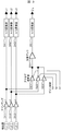
- FIG. 2 shows an example of a configuration of a plurality of spatially independent detectors and signal processing.
- the number of detectors is three. Reflected / scattered light from the sample 8 is guided to the photoelectric conversion surfaces of the detectors 22, 32, and 42 by the detection lenses 21, 31, and 41, respectively.
- the three outputs of the detectors 22, 32 and 42 are combined with the output of the adder 4 to generate four types of signals in this example.
- These signals are digitally encoded by the A / D converters 23, 33, 43, and 53, and then detected from foreign matter and defects by the thresholds Th1, Th2, Th3, and Th4 that are different from each other by the determination processors 24, 34, 44, and 54, respectively. Are distinguished and determined, and the results Df1, Df2, Df3, and Df4 are output.
- FIG. 3 shows an example of the operation and configuration of the adder 4.
- the outputs of the detectors L1, L2, and L3 are output to the outputs L1, L2, and L3 via the gain amplifiers 311, 312, and 313 and the A / D converters 341, 342, and 343, respectively.
- the outputs of the gain amplifiers 311, 312, 313 are input to the addition amplifier 331 via the gain amplifiers 321, 322, 323, and become an output ⁇ L via the A / D converter 351.
- gain values G1, G2, and G3 are set for the detection signals of the detectors so as to maximize the SN ratio of the added signals output from the detectors L1, L2, and L3.
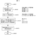
- FIG. 4 shows an example of a calculation process procedure of gain values G1, G2, and G3 that maximize the SN ratio of the addition signal shown in FIG.
- the processing is started (step 401, expressed as S401 in the figure, the same applies hereinafter), the noise signal values L1n, L2n, and L3n of each detector are measured (step 402).
- the minimum noise value is selected from these (step 403). In this example, it is L1n.
- G1 1 (reference)
- G2 L1n / L2n
- a calculated value is set in the gain amplifier of each detector (S405), and the process ends (step 406).
- FIG. 5 shows an example of the operation and configuration of processing when digital data is used.
- the outputs of the detectors L1, L2, and L3 are output to the outputs L1, L2, and L3 via the gain amplifiers 511, 512, and 513 and the A / D converters 521, 522, and 523, respectively. Further, the outputs L1, L2, and L3 become noise detection signals L1n, L2n, and L3n by the noise detection circuit 30, and are input to the minimum value detection circuit 40 and the gain calculation circuit 50. Based on the minimum value selected by the minimum value selection circuit 40 (in the example of FIG. 5, L1n is selected as the minimum value because L1n> L2n> L3n), the gain calculation circuit 50 performs gain calculation processing.
- the gain signals G1, G2, G3 are calculated.
- G3 L1n / L3n.
- the gain calculation circuits 61, 62, and 63 outputs L1, L2, and L3 and gain signals G1, G2, and G3 are input, gain calculation processing is performed based on these, and output signals S1, S2, and S3 are output.
- S3 L3 * (L1n / L3n).
- these output signals S1, S2, S3 are added and outputted as ⁇ S.
- the logic for maximizing the S / N ratio of the sum signal of each detector is the same as that shown in FIG. 4, but in the analog signal processing circuit of FIG. 3, the noise value of each detector is measured in advance and the gain value is set. While it is necessary to calculate and set the gain value for maximizing the S / N ratio of the addition signal of each detector in real time in the configuration of FIG. 5, the setting is made for each more detailed area. The detection sensitivity can be improved.
- FIG. 6 shows an example of the operational configuration of the determination processor.
- An output AD1 of the A / D converter can be stored in the memory 604 by calculating a threshold value Th1r according to an arithmetic logic that is input to the arithmetic unit 603 and set in advance through an arithmetic logic set via the Bus 602 according to an instruction from the CPU 601.
- Memory address generation at the time of writing the threshold value Th1r and reading the threshold value Th1m is performed based on an encoder signal mounted on the inspection stage.
- the inspection position is recognized according to the memory address, and the calculated threshold value corresponding to the inspection position is written into the memory 604 and the inspection threshold value at the time of inspection is read out.
- the memory 604 can be read and written via the bus 602 according to instructions from the CPU 601.
- the register 605 can set the threshold Th1f via the Bus 602 according to an instruction from the CPU 601.
- the threshold value input to the comparator 607 can select any of Th1r, Th1m, and Th1f in the selection circuit 606 based on the selection code SC1 set by the instruction of the CPU 601.
- the selected threshold value Th1 is determined by the output AD1 of the A / D converter and the comparator 607, and if AD1> Th1, the determination result Df1 outputs a code with a defect and a defect data value AD1.
- SC1 selects Th1f to detect a specified size or larger, Th1r to inspect with an optimum threshold according to the surface condition of the object to be inspected, and Th1m to specify inspection sensitivity for each region of the object to be inspected. Threshold selection can be set according to the inspection purpose.
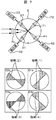
- FIG. 7 shows an example of the optical system configuration and the distribution of reflected / scattered light from the sample when there are four detectors.
- Reflected / scattered light from the sample 8 due to the light irradiated to the sample 8 by the illumination lens 7b passes through the detection lenses 21, 31, 41, 71 arranged at spatially independent positions.
- 32, 42 and 72 are converted into electric signals, respectively.
- the signal intensity output from each detector 22, 32, 42, 72 differs in intensity distribution for each signal intensity distribution map D1s, D2s, D3s, D4s depending on the surface state of the sample, crystal structure, and the like. For each of the signal intensity distribution maps D1s, D2s, D3s, and D4s shown in the lower half of FIG.
- the signal intensity is high in the regions (1), (2), (3), and (4). Yes.
- the threshold value is generated by the determination processor function of FIG. 6 according to the magnitude of the signal intensity, so that the entire surface of the sample can be inspected under optimum conditions regardless of the state of the sample.
- Each of the detectors 22, 32, 42, and 72 can capture the signal of the entire sample surface and inspect it with an optimum threshold corresponding to the signal intensity.
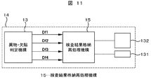
- Fig. 11 shows the reprocessing configuration when there are three detectors. From the foreign matter / defect determination mechanism 13, the inspection results for each of the three detectors and the addition signals of the three detectors are output as four files Df 1 to Df 4 and stored in the inspection result storage / reprocessing mechanism 15.
- the stored file is calculated under the conditions set by the input unit 131 and stored as a new file.
- the calculation conditions are, for example, a logical product such as detection only by the detector (1), detection by the detector (1) and the detector (3), or logical detection such as detection by either the detector (1) or the detector (2).
- There are processes such as sum, larger than specified defect size, smaller or specified defect size range.
- both the above-mentioned AND and defect size conditions can be applied simultaneously.
- the difference in the shape and size of the foreign matter / defect is the difference in the azimuth angle, elevation angle, and scattering intensity of the scattered light.
- the foreign matter / defects can be classified by reprocessing the detected presence / absence of each detector and the defect size under appropriate conditions.
- the comparison of chip data is not used in the detection processing logic, it is not necessary to input information such as chip size and arrangement as the inspection condition, and the optimum value of the inspection threshold is automatically calculated by the function shown in FIG. Therefore, it is possible to greatly shorten the work time for obtaining the inspection conditions.
- the above processing is simultaneously performed according to the detection signal by a plurality of detectors as shown in FIG. 7, and the results of the detectors are added and output in the same manner as the inspection results of the detectors.
- Application Example 3 An application example to inspection of another wafer with a pattern will be described with reference to FIG. As described in Application Example 2, since it is not necessary to input information such as chip size and arrangement as inspection conditions, when the chip arrangement is not in a matrix (houndstooth), or when different types of chips are mixed, or For both inspection samples, an appropriate threshold value is calculated for each of the detectors arranged at spatially different positions and for each inspection region (region P or region NP) by the function shown in FIG. Regardless of the state, it is possible to determine defects and foreign matter.
- an optical inspection apparatus is equipped with a function for setting an inspection threshold for each region and a function for setting an inspection threshold for each of a plurality of spatially independent detectors.
- the detection sensitivity is maximized by maximizing the detection signal S / N ratio by the optimum signal calculation processing and setting the optimum threshold value.
- the noise from the object to be inspected changes depending on the surface state and crystal structure of the object to be inspected, but the detection signal S / N ratio can be maximized and the optimum threshold value can be set by the optimum signal calculation process without being affected by it.
- detection sensitivity can be improved.
- An illumination system for irradiating an object to be inspected with illumination light, a detection unit for detecting scattered light from the object to be inspected, a plurality of spatially independent detectors, and output signals of the plurality of detectors independently And a signal processing unit that performs signal processing under the processed conditions.
- the signal processing unit that performs processing under the independent processing conditions includes a determination processing unit that sets a threshold value independently for each detector of the plurality of detectors and performs determination processing.
- the signal processing unit for processing under the independent processing conditions is configured to perform determination processing by changing a threshold value for determining noise and defects for each detector of the plurality of detectors and for each individual region of the inspected object.
- An inspection apparatus having a determination processing unit. 4). Above 1.
- the inspection apparatus having a display unit that arbitrarily selects each output signal of the plurality of detectors and the signal processing result and displays the result on the same screen. 5). Above 1.
- the inspection apparatus having a signal processing unit that reprocesses signal processing results of a plurality of detectors under an arbitrary condition. 6). Above 1.
- the inspection apparatus for calculating a gain setting value that maximizes the SN ratio of the addition result signal of the output signals from the plurality of detectors and setting the values to the plurality of detectors in the signal processing unit. 7).
- the scattered light from the inspection object is detected by a plurality of spatially independent detectors, and each output signal of the plurality of detectors is detected.
- An inspection method that processes signals under independent processing conditions. 8). Above 7.
- the processing under the independent processing condition is an inspection method in which a threshold value is independently set for each of the detectors of the plurality of detectors for determination processing. 9. Above 7. In this case, the processing under the independent processing conditions is performed by changing the threshold value for discriminating noise and defects for each detector of the plurality of detectors and for each individual region of the inspection object. . 10. Above 7.
- each output signal of the plurality of detectors and the signal processing result are arbitrarily selected and displayed on the same screen.
- the aspect of the present invention is not limited to the above-described embodiments, and various modifications can be made within the scope of the technical idea.
- the present invention is also applied to a case where there is a crystal wall interface in a certain direction like an epitaxial wafer.
- the inspection process may be performed by selecting the information of the detector that outputs the smallest signal among the signals detected from the independent detectors. This is because the scattered light caused by the crystal wall interface should have a directional characteristic, so in any one of a plurality of detectors arranged to cover all directions, this crystal wall interface This is because it can be expected not to detect scattered light caused by the above.
Landscapes
- Physics & Mathematics (AREA)
- Health & Medical Sciences (AREA)
- Life Sciences & Earth Sciences (AREA)
- Chemical & Material Sciences (AREA)
- Analytical Chemistry (AREA)
- Biochemistry (AREA)
- General Health & Medical Sciences (AREA)
- General Physics & Mathematics (AREA)
- Immunology (AREA)
- Pathology (AREA)
- Investigating Materials By The Use Of Optical Means Adapted For Particular Applications (AREA)
Abstract
被検査体の個々の領域に対しノイズの大きさに応じて領域毎に異なる閾値を設定することで表面状態の変化に対応でき検出感度向上を図ることにある。 領域毎に検査閾値を設定する機能を搭載し且つ、空間的に独立した複数の検出器毎に検査閾値を設定する機能を搭載する。被検査体からのノイズの大きさは同じ領域でも空間的な方向によって異なる。よって、検出器毎,被検査体の領域毎に被検査体からのノイズの大きさに応じて最適な信号演算処理による検出信号SN比の最大化と最適な閾値設定を行うことで、検出感度の最大化を図る。
Description
本発明は、光学式検査装置の検査技術に関するものである。例えば、半導体デバイスの製造工程で半導体ウェーハ表面の異物や欠陥などを検査する検査方法,異物や欠陥などを検査する検査装置、及び半導体デバイスの検査方法及び検査装置に関するものである。また、ウェーハ以外のDISKやガラス基板の検査方法及び検査装置に関するものである。
従来の光学式検査装置では、被検査体からの散乱光の大きさに応じて検査閾値を設定するが、被検査体全面で同一の値を設定しているのが一般的である。また、複数の検出器において共通した閾値を使用している。これらに関連するものとして、例えば、特許文献1や特許文献2が挙げられる。
しかしながら、実際の被検査体表面の状態は一様で無く、被検査体全面で一様の検査閾値では、ノイズの最も大きい領域の制約を受けノイズの小さい領域の検出感度を下げる結果となるという課題がある。
本発明の一つの目的は、被検査体の表面状態の変化に対応でき、検出感度向上を図れる検査方法又は検査装置を提供することにある。
本発明の一つの特徴は、被検査体に照明光を照射する照明系と、前記被検査体からの散乱光を検出する検出部と、空間的に独立した複数の検出器と、前記複数の検出器の各出力信号を独立した処理条件で信号処理する信号処理部とを有する検査装置にある。
本発明の他の特徴は、被検査体に照明光を照射して検査する検査方法において、前記被検査体からの散乱光を、空間的に独立した複数の検出器にて検出し、前記複数の検出器の各出力信号を独立した処理条件で信号処理する検査方法にある。
本発明の上記特徴及びその他の特徴は、以下の記載で更に説明される。
本発明の一つの態様によれば、被検査体の表面状態の変化に対応でき、検出感度向上を図れる検査装置を提供することにある。
本発明の他の態様によれば、被検査体の表面状態の変化に対応でき、検出感度向上を図れる検査方法を提供することにある。
以下、図面を用いて、本発明の実施の形態を説明する。
図1に、本発明の実施例である表面検査装置の装置構成の一例を示す。光源1から照射された光は、明るさを調整することができる光量調整機構2,光軸補正機構3、およびズーム機構5を通り、被検査体である試料8に照射される。ズーム機構5から照射された光は垂直斜方照射切り替えミラー6aで垂直光路または斜方光路に切り替えられる。垂直に分岐された光は、集光レンズ7aにて集光され試料8に照射される。試料8は、XYZθステージ9上に搭載される。XYZθステージは、試料表面に平行なX軸およびY軸、試料表面に垂直なZ軸、試料を回転可能にするθ軸の各軸方向に移動可能に構成される。一般には、Z軸方向の動きにより、照射された光を結像するための焦点調整に用いられ、θ軸方向とX軸又はY軸方向との移動により、表面検査走査中は、試料表面に照射された光のスポットが、ウェーハなどの被検査体中心から外周、または外周から中心に向かって螺旋状に移動する。また、θ軸方向とX軸又はY軸方向との移動により、表面検査走査中は、試料表面に照射された光のスポットが、ウェーハなどの被検査体中心から外周、または外周から中心に向かって同心円状に移動する。照射された光による試料8からの反射・散乱光は、検出レンズ10により検出器11に導かれる。その後、検出された光の信号は、A/D変換器12によりデジタル符号化される。その後、異物・欠陥判定機構13による異物・欠陥判定処理にて、試料8からと異物・欠陥からの反射・散乱光による信号を区別・判定し、異物・欠陥を検出する。異物・欠陥判定機構13には、キーボード又はマウスなどの入力部131や検査処理に関する表示を行うディスプレイ又はプリンタなどの出力部132が接続される。検出器11が後述の図2記載のように複数ある場合、出力部132は、複数の検出器の信号および信号処理結果を任意に選択しディスプレイなどの同一画面内に表示できるように構成しても良い。
図2に、空間的に独立した複数の検出器および信号処理の構成の一例を示す。本例では、検出器の数を3個としている。試料8からの反射・散乱光は、検出レンズ21,31,41により、それぞれ、検出器22,32,42の光電変換面に導かれる。検出器22,32,42の3個の出力は、加算器4の出力と併せて本例では4種の信号が生成される。これらの信号はA/D変換器23,33,43,53でデジタル符号化の後、判定処理器24,34,44,54にて各々異なる閾値Th1,Th2,Th3,Th4により異物・欠陥からの反射・散乱光による信号を区別・判定し、結果Df1,Df2,Df3,Df4を出力する。
図3には、加算器4の作用・構成の一例を示す。本例では、検出器L1,L2,L3の3個の検出器としている。検出器L1,L2,L3の出力は、それぞれ、ゲインアンプ311,312,313を経由し、A/D変換器341,342,343を介して、出力L1,L2,L3となる。更に、ゲインアンプ311,312,313の出力は、ゲインアンプ321,322,323を経由し、加算アンプ331に入力され、A/D変換器351を介して、出力ΣLとなる。ゲインアンプ321,322,323については、検出器L1,L2,L3出力の加算信号のSN比を最大化する様に各検出器の検出信号毎にゲイン値G1,G2,G3が設定される。
図4に、図3で示した加算信号のSN比を最大化するゲイン値G1,G2,G3の算出処理手順の一例を示す。処理が開始されると(ステップ401、図中ではS401と表記する。以下同様。)、各検出器のノイズ信号値L1n,L2n,L3nを測定する(ステップ402)。この中から最小値のノイズ値を選択する(ステップ403)。本例ではL1nとする。設定すべきゲインは、最小値を基準=1とし、残りの検出信号のノイズ値がL1nと同じになる値となる。本例ではG1=1(基準),G2=L1n/L2n,G3=L1n/L3nと算出される(ステップ404)。各検出器のゲインアンプに算出値を設定し(S405)、終了となる(ステップ406)。
図5に、デジタルデータを用いた場合の処理の作用・構成の一例を示す。検出器L1,L2,L3の出力は、それぞれ、ゲインアンプ511,512,513を経由し、A/D変換器521,522,523を介して、出力L1,L2,L3となる。さらに、出力L1,L2,L3は、ノイズ検出回路30で、ノイズ検出信号L1n,L2n,L3nとなり、最小値検出回路40およびゲイン算出回路50へ入力される。最小値選択回路40で選択された最小値(図5の例ではL1n>L2n>L3nであるため最小値としてL1nが選択される。)に基づいて、ゲイン算出回路50において、ゲイン算出処理がなされ、ゲイン信号G1,G2,G3が算出される。図5の例では、G1=1,G2=L1n/L2n,G3=L1n/L3nである。ゲイン演算回路61,62,63では、出力L1,L2,L3と、ゲイン信号G1,G2,G3が入力され、それらに基づきゲイン演算処理がなされ、出力信号S1,S2,S3が出力される。図5の例では、S1=L1,S2=L2*(L1n/L2n),S3=L3*(L1n/L3n)である。加算回路70において、これら出力信号S1,S2,S3が加算処理されΣSとして出力される。ΣS=S1=L1+S2+S3となる。各検出器の加算信号のSN比を最大化する論理は図4で示したものと同じであるが、図3のアナログ信号での処理回路では予め各検出器のノイズ値を測定しゲイン値を算出し設定しておく必要があるのに対し、本図5の構成ではリアルタイムで各検出器の加算信号のSN比を最大化するゲイン値が算出できるため、より詳細な領域毎にその設定が可能となり検出感度の向上が実現できる。
図6に、判定処理器の作用構成の一例を示す。A/D変換器の出力AD1は、演算器603に入力され予め設定された演算論理またはCPU601の指示によりBus602を介して設定された演算論理に従い閾値Th1rが算出されメモリ604に格納できる。閾値Th1rの書込みおよび閾値Th1mの読出し時のメモリアドレス生成は検査ステージに実装されているエンコーダ信号を基に行われる。そのメモリアドレスに従い検査位置を認識し検査位置に対応する算出閾値のメモリ604への書込み及び検査時の検査閾値の読出しが行われる。また、メモリ604はCPU601の指示によりBus602を介して読出し、書込みが可能である。レジスタ605はCPU601の指示によりBus602を介して閾値Th1fを設定可能である。比較器607への閾値入力はCPU601の指示により設定された選択コードSC1に基づき選択回路606においてTh1r,Th1m,Th1fのいずれかが選択可能である。選択された閾値Th1はA/D変換器の出力AD1と比較器607で大小判定されAD1>Th1の場合、判定結果Df1は欠陥有りの符号と欠陥データ値AD1を出力する。SC1は指定サイズ以上を検出する場合はTh1f、被検査体の表面状態に応じた最適な閾値で検査する場合はTh1r、被検査体の領域別に検査感度を指定する場合はTh1mを選択する様に検査目的により閾値選択の設定が可能である。
図7に、検出器が4個の場合の光学系構成と試料からの反射・散乱光の分布の一例を示す。照明レンズ7bにより、試料8に照射された光による試料8からの反射・散乱光は、空間的に独立した位置に配置された検出レンズ21,31,41,71を介して、検出器22,32,42,72にて、各々電気信号に変換される。各検出器22,32,42,72から出力される信号強度は、試料の表面状態,結晶構造などにより信号強度分布マップD1s,D2s,D3s,D4s毎に強度分布が異なる。図7下半分に示される、信号強度分布マップD1s,D2s,D3s,D4s毎に、領域(1),領域(2),領域(3),領域(4)で信号強度が高い状態を表している。信号強度の大きさに応じて、前記図6の判定処理器機能により、閾値が生成されることにより、試料全面を試料の状態によらず最適条件で検査可能である。各検出器22,32,42,72は試料全面の信号を取り込み信号強度に対応した最適な閾値で検査可能である。
図11に検出器が3個の場合の再処理構成を示す。異物・欠陥判定機構13からは3つの検出器毎及び3つの検出器の加算信号での検査結果が4つのファイルDf1~Df4として出力され検査結果格納再処理機構15に格納される。格納されたファイルは入力部131より設定された条件にて演算され新しいファイルとして格納される。演算条件は例えば検出器(1)のみで検出、検出器(1)と検出器(3)で検出などの論理積や検出器(1)と検出器(2)のどちらかで検出などの論理和,指定欠陥サイズより大きい,小さい、または指定欠陥サイズ範囲での処理などがある。また、上記の論理積和と欠陥サイズの両条件を同時に適用可能である。検出器(1),検出器(2),検出器(3)は空間的に独立しているため、異物・欠陥の形状,サイズの違いが散乱光の方位角,仰角,散乱強度の違いとして検出され各検出器での検出有無、欠陥サイズを適正な条件で再処理を行うことで異物・欠陥の分類が可能となる。
〔応用例1〕
図8を用いて、ウェーハ外周部の検査への応用例を説明する。ウェーハ外周部の領域EG(例えば、ベベル領域)の検査では、平坦部FTと同一の閾値ではウェーハからのノイズが大きく検査できない。ウェーハ外周部の領域EGのノイズが大きい要因は、主にウェーハが傾斜していることと、表面状態が平坦部FTに比べて粗いことによる。上記領域EGでは、ウェーハからのノイズが大きい検出器は図6を用いて説明した機能により、最適な閾値が計算され、ウェーハ表面からの強度(ノイズ成分)を排除し誤検出なく検査可能となる。また、ウェーハ表面からの入射光は小さい検出器では、図6で示された機能により、適正な閾値が計算され、高感度で欠陥・異物の判定が可能となる。
図8を用いて、ウェーハ外周部の検査への応用例を説明する。ウェーハ外周部の領域EG(例えば、ベベル領域)の検査では、平坦部FTと同一の閾値ではウェーハからのノイズが大きく検査できない。ウェーハ外周部の領域EGのノイズが大きい要因は、主にウェーハが傾斜していることと、表面状態が平坦部FTに比べて粗いことによる。上記領域EGでは、ウェーハからのノイズが大きい検出器は図6を用いて説明した機能により、最適な閾値が計算され、ウェーハ表面からの強度(ノイズ成分)を排除し誤検出なく検査可能となる。また、ウェーハ表面からの入射光は小さい検出器では、図6で示された機能により、適正な閾値が計算され、高感度で欠陥・異物の判定が可能となる。
〔応用例2〕
図9を用いて、パターン付きウェーハの検査への応用例を説明する。パターン付きウェーハについては、検査照明の走査軌跡が螺旋状または同心円となる回転ステージを用いたシステム構成を有する場合は、パターンからの散乱光ノイズはウェーハ回転角度により変化し、散乱光を一つの検出器で電気信号に変換すると、ウェーハの多くの領域でノイズが大きく、ウェーハ上の欠陥・異物の判定ができない、または著しく検出感度が低下する。
図9を用いて、パターン付きウェーハの検査への応用例を説明する。パターン付きウェーハについては、検査照明の走査軌跡が螺旋状または同心円となる回転ステージを用いたシステム構成を有する場合は、パターンからの散乱光ノイズはウェーハ回転角度により変化し、散乱光を一つの検出器で電気信号に変換すると、ウェーハの多くの領域でノイズが大きく、ウェーハ上の欠陥・異物の判定ができない、または著しく検出感度が低下する。
しかし、空間的に異なる位置に複数の検出器を配置し且つウェーハからのノイズに対応し最適な閾値を領域毎に算出し検査することで、チップが形成されているチップ形成領域Pにおいて、パターンからの散乱光が小さい検出器が存在し、図6で示された機能により適正な閾値は計算され欠陥・異物の判定が可能となる。また、チップが形成されていない領域NPにはチップが存在しないため、ウェーハからの散乱光ノイズは低くなり、自動的に検査閾値も小さく、連続的に検査可能となる。ウェーハからの散乱光強度に応じて閾値は自動生成されるため領域P,領域NPの配置パターンや、領域割合によらず、同一の走査シーケンスで検査可能となり、ウェーハの処理枚数の増加が可能となる。
また、検出処理論理にチップデータの比較を用いていないため、検査条件としてチップサイズ,配列などの情報を入力する必要がないことと、図6に示す機能により検査閾値の最適値が自動計算されるため、検査条件出しの作業時間の大幅な短縮が可能である。上記の処理は、図7に示したように複数の検出器で検出信号に応じて同時に行われ、各検出器の結果を足し合せ各検出器の検査結果と同様に出力される。
〔応用例3〕
図10を用いて、別のパターン付きウェーハの検査への応用例を説明する。応用例2で説明したとおり、検査条件としてチップサイズ,配列などの情報を入力する必要がないため、チップの配列がマトリクス状(千鳥格子)でない場合、または異種のチップが混在する場合、またはその両方の検査試料であっても、図6の機能により、空間的に異なる位置に配置された検出器毎、且つ検査領域(領域Pや領域NP)毎に適正な閾値が計算され、試料表面の状態に関わらず欠陥・異物の判定が可能となる。
図10を用いて、別のパターン付きウェーハの検査への応用例を説明する。応用例2で説明したとおり、検査条件としてチップサイズ,配列などの情報を入力する必要がないため、チップの配列がマトリクス状(千鳥格子)でない場合、または異種のチップが混在する場合、またはその両方の検査試料であっても、図6の機能により、空間的に異なる位置に配置された検出器毎、且つ検査領域(領域Pや領域NP)毎に適正な閾値が計算され、試料表面の状態に関わらず欠陥・異物の判定が可能となる。
以上述べたように、本明細書では、例えば、被検査体の個々の領域に対しノイズの大きさに応じて領域毎に異なる閾値を設定することで表面状態の変化に対応でき検出感度向上を図ることが開示される。更に、検出感度の向上はノイズレベルの低減によってなされているため、ノイズ変動に起因して検出再現率が低くなっていた微小な欠陥は、感度の向上により、その検出信号の再現率が向上するため、サイジングのばらつきも改善が可能となる。
また、例えば、光学式検査装置において、領域毎に検査閾値を設定する機能を搭載し且つ、空間的に独立した複数の検出器毎に検査閾値を設定する機能を搭載することが開示される。
また、例えば、被検査体からのノイズの大きさは同じ領域でも空間的な方向によって異なる点に注目し、検出器毎、被検査体の領域毎に被検査体からのノイズの大きさに応じて最適な信号演算処理による検出信号SN比の最大化と最適な閾値設定を行うことで、検出感度の最大化を図ることが開示される。
また、被検査体の表面状態,結晶構造により被検査体からのノイズは領域毎に変化するがそれに影響されずに最適な信号演算処理による検出信号SN比の最大化と最適な閾値設定が可能となり検出感度の向上を実現できることが開示される。
さらに、例えば、以下の特徴が開示される。
1.被検査体に照明光を照射する照明系と、前記被検査体からの散乱光を検出する検出部と、空間的に独立した複数の検出器と、前記複数の検出器の各出力信号を独立した処理条件で信号処理する信号処理部とを有する検査装置。
2.上記1.において、前記独立した処理条件で処理する信号処理部は、前記複数の検出器の検出器毎に、独立して閾値を設定し判定処理する判定処理部を有する検査装置。
3.上記1.において、前記独立した処理条件で処理する信号処理部は、前記複数の検出器の検出器毎に、かつ、被検査体の個別領域毎に、ノイズと欠陥を判別する閾値を変化させて判定処理する判定処理部を有する検査装置。
4.上記1.において、前記複数の検出器の各出力信号および前記信号処理結果を任意に選択し同一画面内に表示する表示部を有する検査装置。
5.上記1.において、複数の検出器の信号処理結果を任意の条件にて再処理する信号処理部を有する検査装置。
6.上記1.において、前記信号処理部において、前記複数の検出器からの出力信号の加算結果信号のSN比が最大となるゲイン設定値を算出し、複数の検出器にその値を設定する検査装置。
7.被検査体に照明光を照射して検査する検査方法において、前記被検査体からの散乱光を、空間的に独立した複数の検出器にて検出し、前記複数の検出器の各出力信号を独立した処理条件で信号処理する検査方法。
8.上記7.において、前記独立した処理条件で処理するとは、前記複数の検出器の検出器毎に、独立して閾値を設定し判定処理する検査方法。
9.上記7.において、前記独立した処理条件で処理するとは、前記複数の検出器の検出器毎に、かつ、被検査体の個別領域毎に、ノイズと欠陥を判別する閾値を変化させて判定処理する検査方法。
10.上記7.において、前記複数の検出器の各出力信号および前記信号処理結果を任意に選択し同一画面内に表示する検査方法。
11.上記7.において、複数の検出器の信号処理結果を任意の条件にて再処理する検査方法。
12.上記7.において、前記複数の検出器からの出力信号の加算結果信号のSN比が最大となるゲイン設定値を算出し、複数の検出器にその値を設定する検査方法。
1.被検査体に照明光を照射する照明系と、前記被検査体からの散乱光を検出する検出部と、空間的に独立した複数の検出器と、前記複数の検出器の各出力信号を独立した処理条件で信号処理する信号処理部とを有する検査装置。
2.上記1.において、前記独立した処理条件で処理する信号処理部は、前記複数の検出器の検出器毎に、独立して閾値を設定し判定処理する判定処理部を有する検査装置。
3.上記1.において、前記独立した処理条件で処理する信号処理部は、前記複数の検出器の検出器毎に、かつ、被検査体の個別領域毎に、ノイズと欠陥を判別する閾値を変化させて判定処理する判定処理部を有する検査装置。
4.上記1.において、前記複数の検出器の各出力信号および前記信号処理結果を任意に選択し同一画面内に表示する表示部を有する検査装置。
5.上記1.において、複数の検出器の信号処理結果を任意の条件にて再処理する信号処理部を有する検査装置。
6.上記1.において、前記信号処理部において、前記複数の検出器からの出力信号の加算結果信号のSN比が最大となるゲイン設定値を算出し、複数の検出器にその値を設定する検査装置。
7.被検査体に照明光を照射して検査する検査方法において、前記被検査体からの散乱光を、空間的に独立した複数の検出器にて検出し、前記複数の検出器の各出力信号を独立した処理条件で信号処理する検査方法。
8.上記7.において、前記独立した処理条件で処理するとは、前記複数の検出器の検出器毎に、独立して閾値を設定し判定処理する検査方法。
9.上記7.において、前記独立した処理条件で処理するとは、前記複数の検出器の検出器毎に、かつ、被検査体の個別領域毎に、ノイズと欠陥を判別する閾値を変化させて判定処理する検査方法。
10.上記7.において、前記複数の検出器の各出力信号および前記信号処理結果を任意に選択し同一画面内に表示する検査方法。
11.上記7.において、複数の検出器の信号処理結果を任意の条件にて再処理する検査方法。
12.上記7.において、前記複数の検出器からの出力信号の加算結果信号のSN比が最大となるゲイン設定値を算出し、複数の検出器にその値を設定する検査方法。
また、本発明の態様は、上記実施例に限定されるものではなく、その技術思想の範囲内において種々変形可能である。例えば、本発明は、エピタキシャルウェーハの様に一定方向に結晶の壁界面がある場合も適用される。この場合は、各独立した検出器から検出された信号のうち最も小さい信号を出力している検出器の情報を選択して検査処理を行うという構成にすればよい。これは、結晶の壁界面に起因した散乱光は方位的に特性を有するはずであるため、全方位を網羅するように配置された複数の検出器のうちのいずれかでは、この結晶の壁界面に起因した散乱光を検出しないことを期待できるためである。
1 光源
2 光量調整機構
3 光軸補正機構
5 ズーム機構
6a 垂直斜方照射切り替えミラー
7a 集光レンズ
8 試料
9 XYZθステージ
10 検出レンズ
11 検出器
12 A/D変換器
13 異物・欠陥判定機構
131 入力部
132 出力部
2 光量調整機構
3 光軸補正機構
5 ズーム機構
6a 垂直斜方照射切り替えミラー
7a 集光レンズ
8 試料
9 XYZθステージ
10 検出レンズ
11 検出器
12 A/D変換器
13 異物・欠陥判定機構
131 入力部
132 出力部
Claims (12)
- 被検査体に照明光を照射する照明系と、
前記被検査体からの散乱光を検出する検出部と、
空間的に独立した複数の検出器と、
前記複数の検出器の各出力信号を独立した処理条件で信号処理する信号処理部とを有することを特徴とする検査装置。 - 請求項1において、
前記独立した処理条件で処理する信号処理部は、前記複数の検出器の検出器毎に、独立して閾値を設定し判定処理する判定処理部を有することを特徴とする検査装置。 - 請求項1において、
前記独立した処理条件で処理する信号処理部は、前記複数の検出器の検出器毎に、かつ、被検査体の個別領域毎に、ノイズと欠陥を判別する閾値を変化させて判定処理する判定処理部を有することを特徴とする検査装置。 - 請求項1において、
前記複数の検出器の各出力信号および前記信号処理結果を任意に選択し同一画面内に表示する表示部を有することを特徴とする検査装置。 - 請求項1において、
複数の検出器の信号処理結果を任意の条件にて再処理する、再処理しないの選択および複数の検出器の信号処理結果を任意の条件にて再処理する信号処理部を有する検査装置。 - 請求項1において、
前記信号処理部において、前記複数の検出器からの出力信号の加算結果信号のSN比が最大となるゲイン設定値を算出し、複数の演算器にその値を設定することを特徴とする検査装置。 - 被検査体に照明光を照射して検査する検査方法において、
前記被検査体からの散乱光を、空間的に独立した複数の検出器にて検出し、
前記複数の検出器の各出力信号を独立した処理条件で信号処理することを特徴とする検査方法。 - 請求項7において、
前記独立した処理条件で処理するとは、前記複数の検出器の検出器毎に、独立して閾値を設定し判定処理することを特徴とする検査方法。 - 請求項7において、
前記独立した処理条件で処理するとは、前記複数の検出器の検出器毎に、かつ、被検査体の個別領域毎に、ノイズと欠陥を判別する閾値を変化させて判定処理することを特徴とする検査方法。 - 請求項7において、
前記複数の検出器の各出力信号および前記信号処理結果を任意に選択し同一画面内に表示することを特徴とする検査方法。 - 請求項7において、
複数の検出器の信号処理結果を任意の条件にて再処理することを特徴とする検査方法。 - 請求項7において、
前記複数の検出器からの出力信号の加算結果信号のSN比が最大となるゲイン設定値を算出し、複数の検出器にその値を設定することを特徴とする検査方法。
Priority Applications (1)
| Application Number | Priority Date | Filing Date | Title |
|---|---|---|---|
| US13/202,708 US8587777B2 (en) | 2009-03-19 | 2009-11-19 | Examination method and examination device |
Applications Claiming Priority (2)
| Application Number | Priority Date | Filing Date | Title |
|---|---|---|---|
| JP2009-067238 | 2009-03-19 | ||
| JP2009067238A JP2010217129A (ja) | 2009-03-19 | 2009-03-19 | 検査方法および検査装置 |
Publications (1)
| Publication Number | Publication Date |
|---|---|
| WO2010106596A1 true WO2010106596A1 (ja) | 2010-09-23 |
Family
ID=42739270
Family Applications (1)
| Application Number | Title | Priority Date | Filing Date |
|---|---|---|---|
| PCT/JP2009/006212 Ceased WO2010106596A1 (ja) | 2009-03-19 | 2009-11-19 | 検査方法および検査装置 |
Country Status (3)
| Country | Link |
|---|---|
| US (1) | US8587777B2 (ja) |
| JP (1) | JP2010217129A (ja) |
| WO (1) | WO2010106596A1 (ja) |
Families Citing this family (5)
| Publication number | Priority date | Publication date | Assignee | Title |
|---|---|---|---|---|
| JP5628010B2 (ja) * | 2010-11-30 | 2014-11-19 | 株式会社日立ハイテクノロジーズ | 欠陥検査装置、判定条件構築装置及び欠陥検査方法 |
| JP5710314B2 (ja) * | 2011-02-25 | 2015-04-30 | 株式会社東芝 | マスク検査方法およびその装置 |
| JP2013238501A (ja) * | 2012-05-16 | 2013-11-28 | Hitachi High-Technologies Corp | 検査装置 |
| JP6353008B2 (ja) * | 2016-11-02 | 2018-07-04 | ファナック株式会社 | 検査条件決定装置、検査条件決定方法及び検査条件決定プログラム |
| US11287375B2 (en) | 2018-04-12 | 2022-03-29 | Hitachi High-Tech Corporation | Inspection device |
Citations (4)
| Publication number | Priority date | Publication date | Assignee | Title |
|---|---|---|---|---|
| JPS63298035A (ja) * | 1987-05-29 | 1988-12-05 | Toshiba Corp | 欠陥検査装置 |
| JPH07113759A (ja) * | 1993-10-14 | 1995-05-02 | Nikon Corp | 異物検査装置 |
| JPH09304289A (ja) * | 1995-04-10 | 1997-11-28 | Hitachi Electron Eng Co Ltd | ウエハ表面検査方法および検査装置 |
| JP2007526444A (ja) * | 2003-06-06 | 2007-09-13 | ケーエルエー−テンカー テクノロジィース コーポレイション | パターン化ウェハまたは非パターン化ウェハおよびその他の検体の検査システム |
Family Cites Families (12)
| Publication number | Priority date | Publication date | Assignee | Title |
|---|---|---|---|---|
| US4820932A (en) * | 1987-06-04 | 1989-04-11 | Owens-Illinois Television Products Inc. | Method of and apparatus for electrooptical inspection of articles |
| JP4306800B2 (ja) * | 1996-06-04 | 2009-08-05 | ケーエルエー−テンカー テクノロジィース コーポレイション | 表面検査用光学走査システム |
| JP3566589B2 (ja) * | 1998-07-28 | 2004-09-15 | 株式会社日立製作所 | 欠陥検査装置およびその方法 |
| JP3784603B2 (ja) * | 2000-03-02 | 2006-06-14 | 株式会社日立製作所 | 検査方法及びその装置並びに検査装置における検査条件設定方法 |
| US6833913B1 (en) * | 2002-02-26 | 2004-12-21 | Kla-Tencor Technologies Corporation | Apparatus and methods for optically inspecting a sample for anomalies |
| US6781688B2 (en) * | 2002-10-02 | 2004-08-24 | Kla-Tencor Technologies Corporation | Process for identifying defects in a substrate having non-uniform surface properties |
| JP4183492B2 (ja) * | 2002-11-27 | 2008-11-19 | 株式会社日立製作所 | 欠陥検査装置および欠陥検査方法 |
| JP2005283190A (ja) * | 2004-03-29 | 2005-10-13 | Hitachi High-Technologies Corp | 異物検査方法及びその装置 |
| US20060192950A1 (en) * | 2004-12-19 | 2006-08-31 | Neil Judell | System and method for inspecting a workpiece surface using combinations of light collectors |
| JP5279992B2 (ja) * | 2006-07-13 | 2013-09-04 | 株式会社日立ハイテクノロジーズ | 表面検査方法及び装置 |
| JP4908995B2 (ja) * | 2006-09-27 | 2012-04-04 | 株式会社日立ハイテクノロジーズ | 欠陥分類方法及びその装置並びに欠陥検査装置 |
| JP4567016B2 (ja) * | 2007-03-28 | 2010-10-20 | 株式会社日立ハイテクノロジーズ | 欠陥検査装置及び欠陥検査方法 |
-
2009
- 2009-03-19 JP JP2009067238A patent/JP2010217129A/ja active Pending
- 2009-11-19 WO PCT/JP2009/006212 patent/WO2010106596A1/ja not_active Ceased
- 2009-11-19 US US13/202,708 patent/US8587777B2/en not_active Expired - Fee Related
Patent Citations (4)
| Publication number | Priority date | Publication date | Assignee | Title |
|---|---|---|---|---|
| JPS63298035A (ja) * | 1987-05-29 | 1988-12-05 | Toshiba Corp | 欠陥検査装置 |
| JPH07113759A (ja) * | 1993-10-14 | 1995-05-02 | Nikon Corp | 異物検査装置 |
| JPH09304289A (ja) * | 1995-04-10 | 1997-11-28 | Hitachi Electron Eng Co Ltd | ウエハ表面検査方法および検査装置 |
| JP2007526444A (ja) * | 2003-06-06 | 2007-09-13 | ケーエルエー−テンカー テクノロジィース コーポレイション | パターン化ウェハまたは非パターン化ウェハおよびその他の検体の検査システム |
Also Published As
| Publication number | Publication date |
|---|---|
| JP2010217129A (ja) | 2010-09-30 |
| US20110299088A1 (en) | 2011-12-08 |
| US8587777B2 (en) | 2013-11-19 |
Similar Documents
| Publication | Publication Date | Title |
|---|---|---|
| US7733474B2 (en) | Defect inspection system | |
| JP5097335B2 (ja) | プロセス変動のモニタシステムおよび方法 | |
| KR102326402B1 (ko) | 포커스 용적 측정 방법을 이용한 웨이퍼 검사 | |
| US9523646B2 (en) | Wafer and reticle inspection systems and methods for selecting illumination pupil configurations | |
| JP5593399B2 (ja) | 計測装置 | |
| JP7427763B2 (ja) | 光学的表面欠陥物質特性評価のための方法およびシステム | |
| JP2001250852A (ja) | 半導体デバイスの製造方法、検査装置における検査条件出し方法、検査装置の選定方法並びに検査装置およびその方法 | |
| JP4567016B2 (ja) | 欠陥検査装置及び欠陥検査方法 | |
| JP2015537218A (ja) | 検出感度改善のための検査ビームの成形 | |
| JP5463943B2 (ja) | 画像データ処理方法および画像作成方法 | |
| WO2010106596A1 (ja) | 検査方法および検査装置 | |
| WO2011105016A1 (ja) | 欠陥検査装置および欠陥検査方法 | |
| JP5349742B2 (ja) | 表面検査方法及び表面検査装置 | |
| JP5655045B2 (ja) | 光学式表面欠陥検査装置及び光学式表面欠陥検査方法 | |
| JP5784796B2 (ja) | 表面検査装置およびその方法 | |
| JP2013224957A (ja) | 検査装置 | |
| JP2012068141A (ja) | 光学式表面欠陥検査装置及び光学式表面欠陥検査方法 | |
| JP4519832B2 (ja) | 欠陥検査装置 | |
| JP2013174575A (ja) | パターン検査装置、及びこれを使用した露光装置の制御方法 | |
| JPH11135583A (ja) | チップのパターン検査装置および方法 | |
| JP2011242310A (ja) | 検査装置、及び検査方法 | |
| JP2008311668A (ja) | 基板又は半導体ウエーハに形成されたパターンの,重ね合わせ誤差検査装置及び重ね合わせ誤差検査方法 | |
| JP2012177714A (ja) | 検査装置 | |
| JP2005203421A (ja) | 基板検査方法及び基板検査装置 | |
| JP2014059310A (ja) | 検査装置 |
Legal Events
| Date | Code | Title | Description |
|---|---|---|---|
| 121 | Ep: the epo has been informed by wipo that ep was designated in this application |
Ref document number: 09841803 Country of ref document: EP Kind code of ref document: A1 |
|
| WWE | Wipo information: entry into national phase |
Ref document number: 13202708 Country of ref document: US |
|
| NENP | Non-entry into the national phase |
Ref country code: DE |
|
| 122 | Ep: pct application non-entry in european phase |
Ref document number: 09841803 Country of ref document: EP Kind code of ref document: A1 |