JP5349742B2 - 表面検査方法及び表面検査装置 - Google Patents
表面検査方法及び表面検査装置 Download PDFInfo
- Publication number
- JP5349742B2 JP5349742B2 JP2006187344A JP2006187344A JP5349742B2 JP 5349742 B2 JP5349742 B2 JP 5349742B2 JP 2006187344 A JP2006187344 A JP 2006187344A JP 2006187344 A JP2006187344 A JP 2006187344A JP 5349742 B2 JP5349742 B2 JP 5349742B2
- Authority
- JP
- Japan
- Prior art keywords
- light
- optical system
- wafer
- inspection object
- inspection
- Prior art date
- Legal status (The legal status is an assumption and is not a legal conclusion. Google has not performed a legal analysis and makes no representation as to the accuracy of the status listed.)
- Expired - Fee Related
Links
Images

Classifications
-
- G—PHYSICS
- G01—MEASURING; TESTING
- G01N—INVESTIGATING OR ANALYSING MATERIALS BY DETERMINING THEIR CHEMICAL OR PHYSICAL PROPERTIES
- G01N21/00—Investigating or analysing materials by the use of optical means, i.e. using sub-millimetre waves, infrared, visible or ultraviolet light
- G01N21/84—Systems specially adapted for particular applications
- G01N21/88—Investigating the presence of flaws or contamination
- G01N21/95—Investigating the presence of flaws or contamination characterised by the material or shape of the object to be examined
- G01N21/9501—Semiconductor wafers
- G01N21/9503—Wafer edge inspection
-
- G—PHYSICS
- G01—MEASURING; TESTING
- G01N—INVESTIGATING OR ANALYSING MATERIALS BY DETERMINING THEIR CHEMICAL OR PHYSICAL PROPERTIES
- G01N21/00—Investigating or analysing materials by the use of optical means, i.e. using sub-millimetre waves, infrared, visible or ultraviolet light
- G01N21/84—Systems specially adapted for particular applications
- G01N21/88—Investigating the presence of flaws or contamination
- G01N21/94—Investigating contamination, e.g. dust
Description
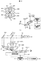
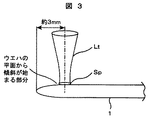
52などよりなる。検査対象となるウェーハ1は、回転テーブル21に載置される。このウェーハ1の上部に配置された検査光学系3は、レーザ発振器を備えたレーザ光源31を有している。これから出力するレーザビームLTは、コリメータレンズ32により平行にされ、第1の投光光学系ではミラー331により反射し、集束レンズ34で収束されたレーザスポットSp(以下スポットSp)として、ウェーハ1の表面へ略垂直に投射される(垂直照射)。また、第2の投光光学系ではレーザビームLTの光路からミラー331を移動し、ミラー332及びミラー35により反射され、集束レンズ36で集束されたレーザスポットSp(以下スポットSp)として、ウェーハ1の表面に斜めに投射される(斜方照射)。垂直照射又は斜方照射されたレーザスポットSpは、ウェーハ1の移動に応じてウェーハを走査する。ウェーハ1は、回転テーブル21,直線移動機構22により回転するとともに回転速度に応じて半径方向(X方向:図中の矢印方向)に移動する。これらにより、スポットSpは、ウェーハ1の表面をスパイラル状に走査し、その結果、ウェーハ1の全面が走査される。なお、回転テーブル21,直線移動機構22の駆動は、駆動制御回路51を介して、データ処理装置52により制御される。
Claims (9)
- 光を円形の被検査物に照射し、前記被検査物から発せられた光を受光して検査する方法において、
前記被検査物の直径方向に発せられた光、及び前記被検査物の接線方向に発せられた光を受光し、
照射した光が被検査物のエッジ領域を照射した場合に、前記直径方向での受光の量を変化させることを特徴とする表面検査方法。 - 請求項1において、
前記受光の量を変化させることは、照射される光の量を変化させること、及び/又は、受光の感度を変化させることであることを特徴とする表面検査方法。 - 請求項1において、
前記受光の量を変化させることは、前記直径方向に配置された受光器をオフ状態とすることであることを特徴とする表面検査方法。 - 請求項1において、
前記受光の量を変化させることは、被検査物エッジ領域からの回折光が少なくなるように受光することを特徴とする表面検査方法。 - 請求項1において、
前記被検査物の上部から略垂直方向に前記光を照射する投光光学系及び/又は前記被検査物の斜めから前記光を照射する投光光学系を有し、前記受光のために複数の受光器を有し、
さらに、前記複数の受光器には、前記被検査物の直径方向に配置された受光器、及び前記被検査物の接線方向に配置された受光器が含まれ、
前記複数の受光器から前記被検査物の接線方向に配置された受光器を選択することを特徴とする表面検査方法。 - 複数の受光器を有する受光系と、
円形の被検査物に対して光を照射する投光光学系と、
前記投光光学系からの光の照射により、前記複数の受光器が検出した信号を演算して異物を識別し、被検査物上の前記光の位置に応じて、前記複数の受光器を選択する手段と、を有し、
さらに、前記複数の受光器には、前記被検査物の直径方向に配置された受光器、及び前記被検査物の接線方向に配置された受光器が含まれ、
前記被検査物のエッジ領域が前記光によって照射された場合には、前記直径方向に配置された受光器の感度を下げる、又は前記直径方向に配置された受光器をオフ状態とし、
前記接線方向に配置された受光器の信号を用いて前記エッジ領域の検査を行うことを特徴とする表面検査装置。 - 請求項6において、
前記受光系は、被検査物の表面を基準とした仰角が30°以下の角度をなす低角度受光系と、前記低角度受光系よりも大きな仰角をなす高角度受光系とを有し、
前記投光光学系は、前記被検査物の上部から略垂直方向にレーザ光を照射する第1の投光光学系と、前記被検査物の斜め方向から偏光したレーザ光を照射する第2の投光光学系とを有し、
前記第1の投光光学系からのレーザ光の照射により、前記高角度受光系が検出した信号を演算して欠陥を識別し、かつ前記第2の投光光学系からの偏光したレーザ光の照射により、前記低角度受光系が検出した信号に基づき異物を識別することを特徴とする表面検査装置。 - 請求項7において、
前記第1の投光光学系の前記レーザ光による走査と前記第2の投光光学系による走査とを切り換える光学系切り換え機構を備えたことを特徴とする表面検査装置。 - 請求項6又は7において、
前記光の前記被検査物上の位置を検知する検知装置を有し、
前記複数の受光器は、前記エッジ領域の回折光の影響を受けない角度に配置された受光器を有し、
前記検知装置の出力に応じて、前記複数の受光器の選択を制御するデータ処理装置を有する表面検査装置。
Priority Applications (3)
| Application Number | Priority Date | Filing Date | Title |
|---|---|---|---|
| JP2006187344A JP5349742B2 (ja) | 2006-07-07 | 2006-07-07 | 表面検査方法及び表面検査装置 |
| US11/822,469 US7616299B2 (en) | 2006-07-07 | 2007-07-06 | Surface inspection method and surface inspection apparatus |
| US12/576,580 US7864310B2 (en) | 2006-07-07 | 2009-10-09 | Surface inspection method and surface inspection apparatus |
Applications Claiming Priority (1)
| Application Number | Priority Date | Filing Date | Title |
|---|---|---|---|
| JP2006187344A JP5349742B2 (ja) | 2006-07-07 | 2006-07-07 | 表面検査方法及び表面検査装置 |
Publications (3)
| Publication Number | Publication Date |
|---|---|
| JP2008014848A JP2008014848A (ja) | 2008-01-24 |
| JP2008014848A5 JP2008014848A5 (ja) | 2008-12-04 |
| JP5349742B2 true JP5349742B2 (ja) | 2013-11-20 |
Family
ID=38918832
Family Applications (1)
| Application Number | Title | Priority Date | Filing Date |
|---|---|---|---|
| JP2006187344A Expired - Fee Related JP5349742B2 (ja) | 2006-07-07 | 2006-07-07 | 表面検査方法及び表面検査装置 |
Country Status (2)
| Country | Link |
|---|---|
| US (2) | US7616299B2 (ja) |
| JP (1) | JP5349742B2 (ja) |
Families Citing this family (15)
| Publication number | Priority date | Publication date | Assignee | Title |
|---|---|---|---|---|
| JP4755040B2 (ja) * | 2006-07-25 | 2011-08-24 | 株式会社神戸製鋼所 | 傷検査装置、傷検査方法 |
| JP5355922B2 (ja) * | 2008-03-31 | 2013-11-27 | 株式会社日立ハイテクノロジーズ | 欠陥検査装置 |
| JP5222635B2 (ja) * | 2008-06-25 | 2013-06-26 | 株式会社日立ハイテクノロジーズ | 被検査物の検査装置及び検査方法 |
| US8089374B2 (en) * | 2008-11-18 | 2012-01-03 | GE Lighting Solutions, LLC | LED signal light |
| US20110317003A1 (en) * | 2010-06-02 | 2011-12-29 | Porat Roy | Method and system for edge inspection using a tilted illumination |
| WO2012082501A2 (en) | 2010-12-16 | 2012-06-21 | Kla-Tencor Corporation | Wafer inspection |
| JP5637841B2 (ja) * | 2010-12-27 | 2014-12-10 | 株式会社日立ハイテクノロジーズ | 検査装置 |
| US9279774B2 (en) | 2011-07-12 | 2016-03-08 | Kla-Tencor Corp. | Wafer inspection |
| CN104080621B (zh) * | 2012-01-31 | 2017-03-08 | 米其林研究和技术股份有限公司 | 模制在浸没的胎面空隙中的突出特征结构 |
| JP5668113B2 (ja) * | 2013-08-28 | 2015-02-12 | 株式会社日立ハイテクノロジーズ | 欠陥検査装置 |
| US9640449B2 (en) * | 2014-04-21 | 2017-05-02 | Kla-Tencor Corporation | Automated inline inspection of wafer edge strain profiles using rapid photoreflectance spectroscopy |
| US10281898B2 (en) * | 2015-07-16 | 2019-05-07 | The Boeing Company | Method and system for controlling automated operations on a workpiece |
| JP6752593B2 (ja) * | 2016-03-07 | 2020-09-09 | 東レエンジニアリング株式会社 | 欠陥検査装置 |
| JP7379104B2 (ja) * | 2019-03-04 | 2023-11-14 | 東京エレクトロン株式会社 | 基板検査装置、基板処理装置、基板検査方法、及びコンピュータ読み取り可能な記録媒体 |
| JP7215411B2 (ja) * | 2019-12-26 | 2023-01-31 | 株式会社Sumco | シリコンウェーハの欠陥検査方法 |
Family Cites Families (29)
| Publication number | Priority date | Publication date | Assignee | Title |
|---|---|---|---|---|
| FR2461944A1 (fr) * | 1979-07-20 | 1981-02-06 | Hitachi Ltd | Procede et appareil pour examiner l'aspect exterieur d'un objet cylindrique plein |
| JPS5722239U (ja) * | 1980-07-11 | 1982-02-04 | ||
| US4598997A (en) * | 1982-02-15 | 1986-07-08 | Rca Corporation | Apparatus and method for detecting defects and dust on a patterned surface |
| US4672196A (en) * | 1984-02-02 | 1987-06-09 | Canino Lawrence S | Method and apparatus for measuring properties of thin materials using polarized light |
| JPS62148945U (ja) * | 1986-03-13 | 1987-09-21 | ||
| US4794264A (en) * | 1987-05-08 | 1988-12-27 | Qc Optics, Inc. | Surface defect detection and confirmation system and method |
| US5144495A (en) * | 1987-12-03 | 1992-09-01 | Compugrade, Inc | Systems for illuminating and evaluating surfaces |
| JP2538338B2 (ja) * | 1989-05-30 | 1996-09-25 | キヤノン株式会社 | 異物検査装置 |
| JP2589411B2 (ja) * | 1990-12-27 | 1997-03-12 | シャープ株式会社 | チップ位置検出方法 |
| JP3126546B2 (ja) * | 1992-04-27 | 2001-01-22 | キヤノン株式会社 | 検査装置と検査方法、並びにこれを用いたシステム |
| US6271916B1 (en) * | 1994-03-24 | 2001-08-07 | Kla-Tencor Corporation | Process and assembly for non-destructive surface inspections |
| JP3686160B2 (ja) * | 1995-04-10 | 2005-08-24 | 株式会社日立ハイテクノロジーズ | ウエハ表面検査方法および検査装置 |
| US5903342A (en) * | 1995-04-10 | 1999-05-11 | Hitachi Electronics Engineering, Co., Ltd. | Inspection method and device of wafer surface |
| CN1299276C (zh) * | 1995-07-27 | 2007-02-07 | 松下电器产业株式会社 | 光盘装置 |
| JPH0989796A (ja) * | 1995-09-21 | 1997-04-04 | Nikon Corp | 光走査装置及び異物検査装置 |
| EP1016126B1 (en) * | 1997-03-31 | 2018-12-26 | Nanometrics Incorporated | Optical inspection module and method for detecting particles and defects on substrates in integrated process tools |
| US6201601B1 (en) * | 1997-09-19 | 2001-03-13 | Kla-Tencor Corporation | Sample inspection system |
| US6104481A (en) * | 1997-11-11 | 2000-08-15 | Kabushiki Kaisha Topcon | Surface inspection apparatus |
| US6990055B1 (en) * | 1999-06-22 | 2006-01-24 | Matsushita Electric Industrial Co., Ltd. | Optical disc drive for controlling reproduction of an optical disc having a plurality of data layers |
| KR100361962B1 (ko) * | 2000-02-03 | 2002-11-23 | (주) 셀라이트 | 웨이퍼 테두리 결함 검사장치 및 검사방법 |
| JP3996728B2 (ja) * | 2000-03-08 | 2007-10-24 | 株式会社日立製作所 | 表面検査装置およびその方法 |
| JP2002098645A (ja) * | 2000-09-26 | 2002-04-05 | Hitachi Electronics Eng Co Ltd | 基板の表面検査装置及び表面検査方法 |
| JP2002188999A (ja) * | 2000-12-21 | 2002-07-05 | Hitachi Ltd | 異物・欠陥検出装置及び検出方法 |
| US7087203B2 (en) * | 2000-11-17 | 2006-08-08 | Nagaoka & Co., Ltd. | Methods and apparatus for blood typing with optical bio-disc |
| US20030002043A1 (en) * | 2001-04-10 | 2003-01-02 | Kla-Tencor Corporation | Periodic patterns and technique to control misalignment |
| US7083920B2 (en) * | 2001-05-18 | 2006-08-01 | Nagaoka & Co. Ltd. | Surface assembly for immobilizing DNA capture probes in genetic assays using enzymatic reactions to generate signal in optical bio-discs and methods relating thereto |
| US7120228B2 (en) * | 2004-09-21 | 2006-10-10 | Jordan Valley Applied Radiation Ltd. | Combined X-ray reflectometer and diffractometer |
| JP4500641B2 (ja) * | 2004-09-29 | 2010-07-14 | 株式会社日立ハイテクノロジーズ | 欠陥検査方法およびその装置 |
| JP2006162500A (ja) * | 2004-12-09 | 2006-06-22 | Hitachi High-Technologies Corp | 欠陥検査装置 |
-
2006
- 2006-07-07 JP JP2006187344A patent/JP5349742B2/ja not_active Expired - Fee Related
-
2007
- 2007-07-06 US US11/822,469 patent/US7616299B2/en active Active
-
2009
- 2009-10-09 US US12/576,580 patent/US7864310B2/en not_active Expired - Fee Related
Also Published As
| Publication number | Publication date |
|---|---|
| JP2008014848A (ja) | 2008-01-24 |
| US20100026996A1 (en) | 2010-02-04 |
| US7616299B2 (en) | 2009-11-10 |
| US7864310B2 (en) | 2011-01-04 |
| US20080007727A1 (en) | 2008-01-10 |
Similar Documents
| Publication | Publication Date | Title |
|---|---|---|
| JP5349742B2 (ja) | 表面検査方法及び表面検査装置 | |
| US10254235B2 (en) | Defect inspecting method and defect inspecting apparatus | |
| JP5355922B2 (ja) | 欠陥検査装置 | |
| US7643139B2 (en) | Method and apparatus for detecting defects | |
| US7733474B2 (en) | Defect inspection system | |
| JP2008216054A (ja) | 被検査物の検査装置及び被検査物の検査方法 | |
| TWI713638B (zh) | 缺陷檢測方法及相關裝置 | |
| JP4638864B2 (ja) | 試料表面の欠陥検査装置 | |
| JP2009283633A (ja) | 表面検査装置及び表面検査方法 | |
| US8101935B2 (en) | Inspection apparatus and inspection method | |
| JP2002188999A (ja) | 異物・欠陥検出装置及び検出方法 | |
| JP2008020371A (ja) | 検査装置 | |
| US8547547B2 (en) | Optical surface defect inspection apparatus and optical surface defect inspection method | |
| JP3432273B2 (ja) | 異物検査装置及び異物検査方法 | |
| JP5222635B2 (ja) | 被検査物の検査装置及び検査方法 | |
| JP5427808B2 (ja) | 検査装置 | |
| JP5668113B2 (ja) | 欠陥検査装置 | |
| JP2011085602A (ja) | 検査装置 | |
| JP2001050720A (ja) | 表面検査方法および装置 | |
| JP2012150024A (ja) | 表面欠陥検査装置及び方法 | |
| JP2003177103A (ja) | 異物検査装置及びdramの製造方法 | |
| JP2015069679A (ja) | 磁気ディスク検査装置及び磁気ディスク検査方法 | |
| JPH06294752A (ja) | ウエーハ表面検査装置 | |
| JP2009170686A (ja) | ウエハ端面検査装置 |
Legal Events
| Date | Code | Title | Description |
|---|---|---|---|
| A521 | Written amendment |
Free format text: JAPANESE INTERMEDIATE CODE: A523 Effective date: 20081014 |
|
| A621 | Written request for application examination |
Free format text: JAPANESE INTERMEDIATE CODE: A621 Effective date: 20081014 |
|
| A521 | Written amendment |
Free format text: JAPANESE INTERMEDIATE CODE: A523 Effective date: 20081014 |
|
| A977 | Report on retrieval |
Free format text: JAPANESE INTERMEDIATE CODE: A971007 Effective date: 20110106 |
|
| A131 | Notification of reasons for refusal |
Free format text: JAPANESE INTERMEDIATE CODE: A131 Effective date: 20110125 |
|
| A521 | Written amendment |
Free format text: JAPANESE INTERMEDIATE CODE: A523 Effective date: 20110513 |
|
| A521 | Written amendment |
Free format text: JAPANESE INTERMEDIATE CODE: A523 Effective date: 20110513 |
|
| A131 | Notification of reasons for refusal |
Free format text: JAPANESE INTERMEDIATE CODE: A131 Effective date: 20120403 |
|
| A521 | Written amendment |
Free format text: JAPANESE INTERMEDIATE CODE: A523 Effective date: 20120528 |
|
| TRDD | Decision of grant or rejection written | ||
| A01 | Written decision to grant a patent or to grant a registration (utility model) |
Free format text: JAPANESE INTERMEDIATE CODE: A01 Effective date: 20130723 |
|
| A61 | First payment of annual fees (during grant procedure) |
Free format text: JAPANESE INTERMEDIATE CODE: A61 Effective date: 20130821 |
|
| R150 | Certificate of patent or registration of utility model |
Free format text: JAPANESE INTERMEDIATE CODE: R150 |
|
| LAPS | Cancellation because of no payment of annual fees |