WO2010103901A1 - 回路基板及びこれを備えた電子装置 - Google Patents
回路基板及びこれを備えた電子装置 Download PDFInfo
- Publication number
- WO2010103901A1 WO2010103901A1 PCT/JP2010/052499 JP2010052499W WO2010103901A1 WO 2010103901 A1 WO2010103901 A1 WO 2010103901A1 JP 2010052499 W JP2010052499 W JP 2010052499W WO 2010103901 A1 WO2010103901 A1 WO 2010103901A1
- Authority
- WO
- WIPO (PCT)
- Prior art keywords
- circuit board
- substrate body
- region
- electronic device
- substrate
- Prior art date
- Legal status (The legal status is an assumption and is not a legal conclusion. Google has not performed a legal analysis and makes no representation as to the accuracy of the status listed.)
- Ceased
Links
Images



Classifications
-
- H—ELECTRICITY
- H05—ELECTRIC TECHNIQUES NOT OTHERWISE PROVIDED FOR
- H05K—PRINTED CIRCUITS; CASINGS OR CONSTRUCTIONAL DETAILS OF ELECTRIC APPARATUS; MANUFACTURE OF ASSEMBLAGES OF ELECTRICAL COMPONENTS
- H05K1/00—Printed circuits
- H05K1/18—Printed circuits structurally associated with non-printed electric components
- H05K1/189—Printed circuits structurally associated with non-printed electric components characterised by the use of flexible or folded printed circuits
-
- H—ELECTRICITY
- H05—ELECTRIC TECHNIQUES NOT OTHERWISE PROVIDED FOR
- H05K—PRINTED CIRCUITS; CASINGS OR CONSTRUCTIONAL DETAILS OF ELECTRIC APPARATUS; MANUFACTURE OF ASSEMBLAGES OF ELECTRICAL COMPONENTS
- H05K1/00—Printed circuits
- H05K1/02—Details
-
- H—ELECTRICITY
- H05—ELECTRIC TECHNIQUES NOT OTHERWISE PROVIDED FOR
- H05K—PRINTED CIRCUITS; CASINGS OR CONSTRUCTIONAL DETAILS OF ELECTRIC APPARATUS; MANUFACTURE OF ASSEMBLAGES OF ELECTRICAL COMPONENTS
- H05K2201/00—Indexing scheme relating to printed circuits covered by H05K1/00
- H05K2201/09—Shape and layout
- H05K2201/09209—Shape and layout details of conductors
- H05K2201/0929—Conductive planes
- H05K2201/09309—Core having two or more power planes; Capacitive laminate of two power planes
-
- H—ELECTRICITY
- H05—ELECTRIC TECHNIQUES NOT OTHERWISE PROVIDED FOR
- H05K—PRINTED CIRCUITS; CASINGS OR CONSTRUCTIONAL DETAILS OF ELECTRIC APPARATUS; MANUFACTURE OF ASSEMBLAGES OF ELECTRICAL COMPONENTS
- H05K2201/00—Indexing scheme relating to printed circuits covered by H05K1/00
- H05K2201/09—Shape and layout
- H05K2201/09209—Shape and layout details of conductors
- H05K2201/09654—Shape and layout details of conductors covering at least two types of conductors provided for in H05K2201/09218 - H05K2201/095
- H05K2201/09781—Dummy conductors, i.e. not used for normal transport of current; Dummy electrodes of components
-
- H—ELECTRICITY
- H05—ELECTRIC TECHNIQUES NOT OTHERWISE PROVIDED FOR
- H05K—PRINTED CIRCUITS; CASINGS OR CONSTRUCTIONAL DETAILS OF ELECTRIC APPARATUS; MANUFACTURE OF ASSEMBLAGES OF ELECTRICAL COMPONENTS
- H05K2201/00—Indexing scheme relating to printed circuits covered by H05K1/00
- H05K2201/10—Details of components or other objects attached to or integrated in a printed circuit board
- H05K2201/10227—Other objects, e.g. metallic pieces
- H05K2201/10409—Screws
-
- H—ELECTRICITY
- H05—ELECTRIC TECHNIQUES NOT OTHERWISE PROVIDED FOR
- H05K—PRINTED CIRCUITS; CASINGS OR CONSTRUCTIONAL DETAILS OF ELECTRIC APPARATUS; MANUFACTURE OF ASSEMBLAGES OF ELECTRICAL COMPONENTS
- H05K2201/00—Indexing scheme relating to printed circuits covered by H05K1/00
- H05K2201/10—Details of components or other objects attached to or integrated in a printed circuit board
- H05K2201/10431—Details of mounted components
- H05K2201/10598—Means for fastening a component, a casing or a heat sink whereby a pressure is exerted on the component towards the PCB
-
- H—ELECTRICITY
- H05—ELECTRIC TECHNIQUES NOT OTHERWISE PROVIDED FOR
- H05K—PRINTED CIRCUITS; CASINGS OR CONSTRUCTIONAL DETAILS OF ELECTRIC APPARATUS; MANUFACTURE OF ASSEMBLAGES OF ELECTRICAL COMPONENTS
- H05K2201/00—Indexing scheme relating to printed circuits covered by H05K1/00
- H05K2201/20—Details of printed circuits not provided for in H05K2201/01 - H05K2201/10
- H05K2201/2009—Reinforced areas, e.g. for a specific part of a flexible printed circuit
-
- H—ELECTRICITY
- H05—ELECTRIC TECHNIQUES NOT OTHERWISE PROVIDED FOR
- H05K—PRINTED CIRCUITS; CASINGS OR CONSTRUCTIONAL DETAILS OF ELECTRIC APPARATUS; MANUFACTURE OF ASSEMBLAGES OF ELECTRICAL COMPONENTS
- H05K3/00—Apparatus or processes for manufacturing printed circuits
- H05K3/46—Manufacturing multilayer circuits
- H05K3/4611—Manufacturing multilayer circuits by laminating two or more circuit boards
- H05K3/4626—Manufacturing multilayer circuits by laminating two or more circuit boards characterised by the insulating layers or materials
- H05K3/4632—Manufacturing multilayer circuits by laminating two or more circuit boards characterised by the insulating layers or materials laminating thermoplastic or uncured resin sheets comprising printed circuits without added adhesive materials between the sheets
Definitions
- the present invention relates to a circuit board and an electronic device including the circuit board, and more particularly to a circuit board on which electronic components are mounted on the surface and an electronic device including the circuit board.
- FIG. 9 is an exploded perspective view of the electronic apparatus 510 including the printed circuit board 512 described in Patent Document 1.
- FIG. 10 is an external perspective view of the electronic device 510 described in Patent Document 1.
- the electronic device 510 includes a printed circuit board 512, a lid body 514, and a frame body 516 as shown in FIG.
- the printed circuit board 512 includes rigid portions 512a and 512b and a flexible portion 512c.
- the rigid portions 512a and 512b are rectangular hard substrates made of resin, ceramic, or the like.
- Electronic components (not shown) are mounted on the main surfaces of the rigid portions 512a and 512b.
- the flexible part 512c is made of a flexible material and incorporates a wiring for connecting the rigid parts 512a and 512b.
- the lid body 514 and the frame body 516 form a rectangular parallelepiped housing by being assembled, and have a printed circuit board 512 built therein.
- the frame 516 has claws 518 (518a to 518d) and 520 (520a to 520d).
- the claws 518 and 520 are protrusions protruding inward on the side surface of the frame body 516, and hold the rigid portions 512a and 512b.
- the printed circuit board 512 is bent in two at the flexible portion 512c.
- the rigid portion 512 b is held by the frame body 516 by being engaged with the claw 518.
- the rigid portion 512 a is held by the frame body 516 by being engaged with the claw 520.
- the electronic components on the rigid portions 512a and 512b may come off as described below. is there. More specifically, when the rigid portions 512a and 512b are engaged with the claws 518 and 520, the rigid portions 512a and 512b are pushed into the frame body 516 from above by the assembler. At this time, the rigid portion 512b and the claw 518 are elastically deformed, so that the rigid portion 512b is fitted below the claw 518. Similarly, the rigid portion 512a and the claw 520 are elastically deformed, so that the rigid portion 512a is fitted below the claw 520.
- the rigid portions 512a and 512b are hard substrates made of resin, ceramic, or the like. Therefore, the entire rigid parts 512a and 512b are bent at the time of attachment to the frame body 516.
- the electronic component is soldered on the rigid parts 512a and 512b. Therefore, the solder is damaged when the rigid portions 512a and 512b are bent. As a result, the electronic component is detached from the rigid portions 512a and 512b.
- a multilayer wiring board described in Patent Document 2 and a flexible printed circuit board described in Patent Document 3 are known.
- the multilayer wiring board (flexible printed circuit board) is attached to the case with screws. Even in such a multilayer wiring board (flexible printed circuit board), when being fixed to the case, the board is bent by the force from the screw. As a result, the electronic components on the board may be removed.
- an object of the present invention is to provide a circuit board capable of suppressing the mounted electronic component from being detached when attached to the electronic device, and an electronic device including the circuit board.
- a circuit board according to an aspect of the present invention is a circuit board that is mounted on an electronic device and includes a first board body made of a flexible material, and the first board body is an electronic device.
- An electronic device is provided in the circuit board, the electronic device main body, and the electronic device main body, and is fixed to the electronic device main body by contacting the fixing region. And a fixing member.
- the present invention it is possible to prevent the electronic components mounted on the circuit board from being detached when attached to the electronic device.
- FIG. 1 is an external perspective view of a circuit board according to an embodiment of the present invention. It is a disassembled perspective view of the circuit board of FIG. It is a perspective view in the manufacture process of the flexible sheet
- FIG. 5 is a cross-sectional structure diagram along AA in FIG. 4.
- FIG. 5 is a cross-sectional structure view taken along line BB in FIG. 4.
- 1 is an external perspective view of an electronic device described in Patent Document 1.
- FIG. 1 is an external perspective view of a circuit board 10a according to an embodiment of the present invention.
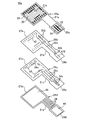
- FIG. 2 is an exploded perspective view of the circuit board 10a of FIG.
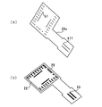
- FIG. 3 is a perspective view in the process of manufacturing the flexible sheet 26a of the circuit board 10a.
- 3A shows the back surface of the flexible sheet 26a
- FIG. 3B shows the surface of the flexible sheet 26a in a state where the resist films 20 and 24 are not formed.
- the surface of the flexible sheet 26 refers to a surface positioned on the upper side in the stacking direction
- the back surface of the flexible sheet 26 refers to a surface positioned on the lower side in the stacking direction.
- the resist films 20 and 24 are hatched for easy understanding of the presence or absence of the resist films 20 and 24.
- the circuit board 10a includes board bodies 12 and 14 and a connection portion 16 as shown in FIG.
- the substrate body 12 has a rectangular shape, and is a rigid substrate on which a plurality of chip components 50 and an integrated circuit 52 are mounted.
- the board body 14 has a rectangular shape smaller than that of the board body 12 and is a rigid board on which the connector 54 is mounted.
- the connection portion 16 is a flexible substrate that connects the substrate body 12 and the substrate body 14. As shown in FIG. 2, the substrate main bodies 12 and 14 and the connecting portion 16 are made of a flexible sheet 26 (26a to 26a) made of a plurality of (four in FIG. 26d) is overlapped. Therefore, the substrate bodies 12 and 14 and the connection portion 16 have the same thickness (the thickness of the four flexible sheets 26).
- the substrate body 12 is configured by stacking substrate sheets 27a to 27d of flexible sheets 26a to 26d.
- the substrate body 12 includes a resist film 20, dummy wirings 22, lands 28, wiring conductors 30 (30b, 30c), a ground conductor 36, and via-hole conductors b1 to b3.
- the wiring conductor 30 and the via-hole conductors b1 to b3 are provided with reference numerals only for representative ones in order to prevent the drawings from becoming complicated.
- the substrate body 12 has a mounting area E1, a variable area E2, and a fixed area E3 on its main surface.
- the mounting region E1 is a region where the chip component 50 and the integrated circuit 52 are mounted, and has a rectangular shape that is slightly smaller than the substrate body 12.
- the variable area E ⁇ b> 2 is provided along the outer periphery of the substrate body 12. That is, the variable area E2 surrounds the mounting area E1. Further, the chip component 50 and the integrated circuit 52 are not mounted in the variable region E2.
- the fixed region E3 is included in the variable region E2, and is a region where a fixing member provided in the electronic device comes into contact, as will be described later.
- the land 28 is a conductor layer provided on the surface of the substrate sheet 27a as shown in FIG. As shown in FIG. 1, the chip component 50 and the integrated circuit 52 are mounted on the land 28 by soldering. Therefore, the land 28 is provided in the mounting area E1.
- the resist film 20 is an insulating film that is provided on the surface of the substrate sheet 27a so as to cover the mounting region E1 and protects the substrate sheet 27a. However, the resist film 20 is not provided on the land 28.
- the resist film 20 is produced, for example, by applying a resin.
- the dummy wiring 22 is a surface conductor layer provided on the boundary between the mounting region E1 and the variable region E2 on the surface of the substrate sheet 27a.
- the dummy wiring 22 is not connected to the land 28 or other wiring.
- the dummy wiring 22 is provided so as to overlap the outer edge of the resist film 20 and surround the resist film 20.
- the wiring conductors 30b and 30c are conductor layers provided on the surfaces of the substrate sheets 27b and 27c, respectively, as shown in FIG. As shown in FIGS. 2 and 3A, the via-hole conductors b1 to b3 are provided so as to penetrate the substrate sheets 27a to 27c in the stacking direction. The wiring conductors 30b and 30c and the via-hole conductors b1 to b3 are connected to each other to form a circuit by laminating the substrate sheets 27a to 27d.
- the ground conductor 36 is a single solid electrode having a large area provided in a portion overlapping the mounting region E1 on the surface of the substrate sheet 27d.
- the ground conductor 36 defines a mounting area E1 in the substrate body 12. That is, the ground conductor 36 has a shape that coincides with the mounting region E1 when viewed in plan from the normal direction of the main surface of the substrate body 12.
- the ground conductor 36 is kept at a ground potential by being grounded.
- the ground conductor 36 is connected to a circuit composed of the wiring conductors 30b and 30c and the via-hole conductors b1 to b3 via the via-hole conductor b3.
- Conductive patterns such as the ground conductor 36, the dummy wiring 22, the land 28, and the wiring conductor 30 are formed by patterning a metal foil such as a copper foil by photolithography or the like, and are harder than the flexible sheet 26.
- the substrate body 14 is configured by stacking substrate sheets 29a to 29d of flexible sheets 26a to 26d.
- the substrate body 14 includes a resist film 24, lands 33, wiring conductors 34 (34b, 34c), a ground conductor 40, and via-hole conductors b11, b12. 1 to 3, the wiring conductor 34 and the via-hole conductors b11 and b12 are provided with reference numerals only for representative ones in order to prevent the drawings from becoming complicated.
- the land 33 is a conductor layer provided on the surface of the substrate sheet 29a as shown in FIG. As shown in FIG. 1, a connector 54 is mounted on the land 28 by soldering.
- the resist film 24 is an insulating film that is provided on the surface of the substrate sheet 29a and protects the substrate sheet 29a. However, the resist film 24 is not provided on the land 33.
- the resist film 24 is produced, for example, by applying a resin.
- the wiring conductors 34b and 34c are conductor layers provided on the surfaces of the substrate sheets 29b and 29c, respectively, as shown in FIG. As shown in FIGS. 2 and 3A, the via-hole conductors b11 and b12 are provided so as to penetrate through the substrate sheets 29a and 29b in the stacking direction. The wiring conductors 34b and 34c and the via hole conductors b11 and b12 are connected to each other to form a circuit by laminating the substrate sheets 29a to 29d.
- the ground conductor 40 is a single solid electrode provided on the surface of the substrate sheet 29d.
- the ground conductor 40 may be provided on the plurality of substrate sheets 29.
- connection unit 16 As shown in FIG. 2, the connection part 16 is configured by overlapping connection sheets 31a to 31d of flexible sheets 26a to 26d. Moreover, the connection part 16 is provided with the wiring conductor 32 (32b, 32c) and the ground conductor 38, as shown in FIG.1 and FIG.2.
- the wiring conductors 32b and 32c are conductor layers provided on the surfaces of the connection sheets 31b and 31c, respectively, as shown in FIG. As shown in FIG. 2, the wiring conductor 32b connects the wiring conductor 30b and the wiring conductor 34b. Further, as shown in FIG. 2, the wiring conductor 32c connects the wiring conductor 30c and the wiring conductor 34c.
- the ground conductor 38 is a conductor layer provided on the surface of the connection sheet 31 d and connecting the ground conductor 36 and the ground conductor 40.
- the ground conductor 38 and the wiring conductors 32b and 32c overlap each other when viewed in plan from the stacking direction, thereby forming a microstrip line. As a result, impedance matching is achieved between the circuit in the substrate body 12 and the circuit in the substrate body 14.
- the grounding conductor 36 that is harder than the flexible sheet 26 is provided in the mounting region E1.
- a resist film 20 that is harder than the flexible sheet 26 is provided in the mounting region E1.
- the ground conductor 36 and the resist film 20 are not provided in the variable region E2 and the fixed region E3. Therefore, the variable region E2 and the fixed region E3 have a structure that is more easily deformed than the mounting region E1.
- the variable region E2 is continuously provided all around the substrate body 12, the connection portion 16, and the substrate body 14 that constitute the circuit board 10a.
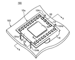
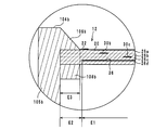
- FIG. 4 is an external perspective view of the electronic device 100.
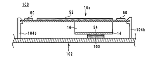
- FIG. 5 is a sectional structural view taken along line AA in FIG.
- FIG. 6 is a cross-sectional structural view taken along line BB in FIG.
- FIG. 4 is an enlarged view of the vicinity of the circuit board 10a.
- the electronic device 100 is, for example, a mobile phone or a personal computer, and includes a circuit board 10a, an electronic device main body 102, and fixing members 104 (104a to 104d) as shown in FIG.
- the electronic device main body 102 is a main body such as a mobile phone or a personal computer.
- the electronic device main body 102 shown in FIG. 4 is a mother board such as a mobile phone or a personal computer.
- the circuit board 10a is mounted on the electronic device main body 102 in a U-shaped state.
- the substrate body 14 wraps around the lower side of the substrate body 12 when the connecting portion 16 is bent.
- a connector 103 is provided on the main surface of the electronic device main body 102 as shown in FIG.
- a connector 54 mounted on the board body 14 is connected to the connector 103.
- the circuit board 10a and the electronic apparatus main body 102 are electrically connected.
- the substrate body 12 is fixed by a fixing member 104.
- the fixing member 104 extends upward from the main surface of the electronic device main body 102, and comes into contact with the main surface of the substrate main body 12 in the vicinity of the upper end. 12 is held.
- the fixing member 104 is provided so as to come into contact with two opposite sides of the circuit board 10a.
- the fixing member 104a and the fixing member 104c face each other with the circuit board 10a interposed therebetween
- the fixing member 104b and the fixing member 104d face each other with the circuit board 10a interposed therebetween.
- the fixing member 104b includes a support shaft 105b and claw-like members 106b and 108b.
- the support shaft 105 b is a member that extends vertically upward from the main surface of the electronic device main body 102.
- the claw-like members 106b and 108b are protrusions that protrude in the same direction with a predetermined gap left in the horizontal direction from the support shaft 105b.
- the predetermined gap is the thickness of the substrate body 12.
- the fixing member 104b holds the substrate body 12 by sandwiching the outer edge of the substrate body 12 between the claw-like member 106b and the claw-like member 108b.
- a region where the claw-like member 106b is in contact with the upper surface of the substrate body 12 is referred to as a fixed region E3.
- the fixed region E ⁇ b> 3 is provided in contact with two opposite sides of the circuit board 10 a.
- circuit board manufacturing method below, the manufacturing method of the circuit board 10a is demonstrated, referring drawings.
- a case where one circuit board 10a is manufactured will be described as an example, but actually, a plurality of circuit boards 10a are simultaneously manufactured by laminating and cutting large-sized flexible sheets.
- a flexible sheet 26 having a copper foil formed on the entire surface is prepared.
- the via holes are formed by irradiating a laser beam from the back side to the positions (see FIGS. 2 and 3A) where the via hole conductors b1 to b3 of the flexible sheets 26a to 26c are formed.
- the dummy wiring 22 and the lands 28 and 33 shown in FIG. 3B are formed on the surface of the flexible sheet 26a by a photolithography process. Specifically, a resist having the same shape as the dummy wiring 22 and the lands 28 and 33 shown in FIG. 3B is printed on the copper foil of the flexible sheet 26a. And the copper foil of the part which is not covered with the resist is removed by performing an etching process with respect to copper foil. Thereafter, the resist is removed. As a result, dummy wirings 22 and lands 28 and 33 are formed on the surface of the flexible sheet 26a as shown in FIG. Furthermore, the resist films 20 and 24 shown in FIGS.
- 1 and 2 are formed by applying a resin to a region surrounded by the dummy wirings 22 on the surface of the flexible sheet 26a.
- the resin is applied so that the resist film 20 slightly overlaps the dummy wiring 22 as well.
- wiring conductors 30b, 32b, and 34b shown in FIG. 2 are formed on the surface of the flexible sheet 26b by a photolithography process. Further, wiring conductors 30c, 32c, and 34c shown in FIG. 2 are formed on the surface of the flexible sheet 26c by a photolithography process. Further, the ground conductors 36, 38, and 40 shown in FIG. 2 are formed on the surface of the flexible sheet 26d by a photolithography process. Note that these photolithography processes are the same as the photolithography processes for forming the dummy wirings 22 and the lands 28 and 33, and thus description thereof is omitted.
- the via holes formed in the flexible sheets 26a to 26c are filled with a conductive paste mainly composed of copper to form via hole conductors b1 to b3 shown in FIGS. 2 and 3A.
- the flexible sheets 26a to 26d are stacked in this order. Then, the flexible sheets 26a to 26d are pressure-bonded by applying a force from above and below to the flexible sheets 26a to 26d. Thereby, the circuit board 10a shown in FIG. 1 is obtained.
- the chip component 50 and the integrated circuit 52 can be prevented from being detached from the board body 12 when attached to the electronic device 100 as described below. More specifically, when the circuit board 10 a is attached to the electronic device 100, the board body 12 is set on the fixing member 104 and the board body 12 is pressed against the fixing member 104. As a result, the fixing member 104 and the substrate body 12 are elastically deformed, and the substrate body 12 enters between the claw-like members 106 and 108. As a result, the substrate body 12 is held by the fixing member 104.
- the substrate body 12 is elastically deformed when pressed against the fixing member 104. At this time, if the entire substrate body 12 has a uniform hardness, the entire substrate body 12 is bent. As a result, the solder that fixes the chip component 50 and the integrated circuit 52 to the substrate body 12 may be damaged, and the chip component 50 and the integrated circuit 52 may be detached from the substrate body 12.
- the fixing region E3 with which the fixing member 104 contacts has a structure that is more easily deformed by an external force than the mounting region E1 in which the chip component 50 and the integrated circuit 52 are mounted.
- the fixing region E ⁇ b> 3 with which the fixing member 104 comes into contact is a portion where the load is most applied to the substrate body 12 when the substrate body 12 is pressed against the fixing member 104.
- the fixed region E3 is configured to be more easily deformed than the mounting region E1, so that the fixed region E3 is elastically deformed and the mounting region E1 is hardly deformed.
- the mounting region E ⁇ b> 1 is deformed, and the chip component 50 and the integrated circuit 52 are prevented from being detached from the substrate body 12.
- the variable area E2 having a structure that is more easily deformed than the mounting area E1 includes the fixed area E3 and is provided along the outer periphery of the board body 12. For this reason, when the substrate body 12 is pressed against the fixing member 104, the fixing region E3 is deformed, and the portion adjacent to the fixing region E3 in the variable region E2 is also deformed. As a result, deformation of the mounting region E1 is more effectively suppressed.
- variable region E2 is provided along the outer periphery of the substrate body 12. Therefore, even if the substrate body 12 is set on the fixed member 104 in a shifted state, the fixed member 104 is in contact with the variable region E2. Therefore, when the board body 12 is pressed against the fixing member 104, the variable area E2 is deformed and the mounting area E1 is prevented from being deformed. Therefore, it is not necessary to set the board body 12 with high accuracy, and the circuit board 10a can be easily attached to the electronic device 100.
- the resist film 20 is provided in the mounting area E1, but not in the variable area E2 and the fixed area E3. Therefore, the variable region E2 and the fixed region E3 are more easily deformed by the resist film 20 than the mounting region E1.
- the chip component 50 and the integrated circuit 52 are prevented from being detached from the board body 12 due to an impact when the electronic device 100 is dropped, as will be described below. More specifically, when the electronic device 100 falls, an impact is transmitted to the substrate body 12 via the fixing member 104. The substrate body 12 is elastically deformed by this impact.
- the fixing region E3 with which the fixing member 104 is in contact has a structure that is more easily deformed than the mounting region E1.
- the variable region E2 includes a fixed region E3 and is provided along the outer periphery of the substrate body 12. Therefore, when the substrate body 12 is elastically deformed, the variable region E2 and the fixed region E3 are deformed, and the mounting region E1 is hardly deformed. As a result, the chip component 50 and the integrated circuit 52 are prevented from being detached from the substrate body 12 due to an impact when the electronic device 100 is dropped.
- the fixing member 104 is in contact with the sides facing each other in the substrate body 12. Therefore, the force exerted by the fixing members 104a and 104c on the substrate body 12 and the force exerted by the fixing members 104b and 104d on the substrate body 12 are balanced in the opposite directions. As a result, the substrate body 12 is stably held by the fixing member 104.
- the fixing members 104a and 104c are provided so as to face each other with the substrate body 12 interposed therebetween, as shown in FIG.
- the fixing members 104b and 104d are provided so as to face each other with the circuit board 10a interposed therebetween. Therefore, when viewed from the center of the base body 12 (intersection of diagonal lines), the moment that the fixing member 104a exerts on the substrate body 12 and the moment that the fixing member 104c exerts on the substrate body 12 are balanced. Furthermore, the moment that the fixing member 104b exerts on the substrate body 12 and the moment that the fixing member 104d exerts on the substrate body 12 are balanced. As a result, the moment of rotation of the substrate body 12 is canceled, and the substrate body 12 is more stably held by the fixing member 104.
- the ground conductor 36 is provided in the mounting area E1 and the ground conductor 36 is provided in the variable area E2 and the fixed area E3 so that the variable area E2 and the fixed area E3 are more easily deformed than the mounting area E1.
- the ground conductor 36 which is an existing component is used, and a new configuration is not added. As a result, the circuit board 10a can be downsized.
- the circuit board 10a can be reduced in thickness and weight as described below. More specifically, in the printed circuit board 512 shown in FIG. 9, the rigid portions 512a and 512b are configured by sandwiching a flexible sheet between two substrates such as a resin. Therefore, the rigid portions 512a and 512b have a total thickness of the flexible sheet and the two substrates. Similarly, the rigid portions 512a and 512b have a total weight of the flexible sheet and the two substrates.
- the board body 12 has only the thickness of the flexible sheet 26.
- the flexible sheet 26 is thinner and lighter than a substrate made of resin or the like. Therefore, the substrate body 12 is thinner than the rigid parts 512a and 512b. Similarly, the substrate body 12 is lighter than the rigid portions 512a and 512b. Therefore, the circuit board 10a can be reduced in thickness and weight.
- circuit board and the electronic device including the circuit board according to the present invention are not limited to those described in the above embodiment, and can be changed within the scope of the gist thereof.
- circuit boards according to other embodiments and electronic devices including the circuit boards will be described.
- FIG. 7 is an external perspective view of a circuit board 10b according to another embodiment.
- the difference between the circuit board 10b and the circuit board 10a is the shape of the variable region E2. More specifically, in the circuit board 10a, the variable region E2 is provided along the outer periphery of the board body 12. On the other hand, in the circuit board 10b, the variable region E2 is provided only in the fixed region E3 and a part of the region adjacent to the fixed region E3. Even in the circuit board 10b having the above-described configuration, the chip component 50 and the integrated circuit 52 are prevented from being detached from the board body 12 in the same manner as the circuit board 10a. Furthermore, the variable area E2 is narrower in the circuit board 10b than in the circuit board 10a. Therefore, the circuit board 10b can have a larger mounting area E1 than the circuit board 10a.
- FIG. 8 is an external perspective view of a circuit board 10c according to another embodiment.
- the difference between the circuit board 10 c and the circuit board 10 a is a method of attaching to the electronic device main body 102. More specifically, the circuit board 10 a is attached to the electronic device main body 102 by being sandwiched between the fixing members 104. On the other hand, the circuit board 10c is attached to the electronic device main body 102 by screws 204 (204a to 204d). In this case, the part where the screw 204 contacts the substrate body 12 is around the screw hole. Therefore, in the circuit board 10c, the fixing region E3 is provided in an annular shape around the screw hole.
- the fixing region E3 around the screw hole is more easily deformed than the mounting region E1. Accordingly, the fixing region E3 is deformed by the force from the screw 204, and the mounting region E1 is hardly deformed. As a result, the circuit board 10 c can suppress the chip component 50 and the integrated circuit 52 from being detached from the board body 12.
- the mounting area E1 is defined by the ground conductor 36.
- the mounting region E1 may be defined by something other than the ground conductor 36, and may be defined by the resist film 20 or the dummy wiring 22, for example.
- the ground conductor 36 is provided in the mounting region E1, and the ground conductor 36 is not provided in the variable region E2 and the fixed region E3, so that the variable region E2 and the fixed region E3 are deformed more than the mounting region E1. It has a structure that is easy to do.
- an internal conductor layer such as a capacitor conductor or a dummy conductor may be used.
- the ground conductor 36 is provided in the mounting region E1, and the ground conductor 36 is not provided in the variable region E2 and the fixed region E3, so that the variable region E2 and the fixed region E3 are more than the mounting region E1. It is easy to deform.
- the method of making the variable area E2 and the fixed area E3 easier to deform than the mounting area E1 is not limited to this.
- the ratio of the area of the mounting region E1 where the internal conductor layer is provided is the same as that of the variable region E2 and the fixed region E3. What is necessary is just to become higher than the ratio of the area of the part which has. Therefore, an internal conductor layer such as the ground conductor 36 may be provided in the variable region E2 and the fixed region E3.
- a resist film 20 or a resin substrate may be used instead of the internal conductor layer such as the ground conductor 36.
- the claw-like member 106 b is not in contact with the dummy wiring 22. However, the claw-like member 106 b may be in contact with the dummy wiring 22. A region where the dummy wiring 22 is provided is less likely to be deformed than a region where the dummy wiring 22 is not provided. Therefore, the claw-like member 106 b comes into stronger pressure contact with the substrate body 12 by contacting the dummy wiring 22. As a result, the substrate body 12 is firmly fixed by the electronic device body 102.
- the present invention is useful for a circuit board and an electronic device equipped with the circuit board, and is particularly excellent in that it can prevent the mounted electronic component from being detached during the mounting to the electronic device.
Landscapes
- Engineering & Computer Science (AREA)
- Microelectronics & Electronic Packaging (AREA)
- Structure Of Printed Boards (AREA)
- Non-Metallic Protective Coatings For Printed Circuits (AREA)
- Mounting Of Printed Circuit Boards And The Like (AREA)
Abstract
Description
以下に、本発明の一実施形態に係る回路基板の構成について図面を参照しながら説明する。図1は、本発明の一実施形態に係る回路基板10aの外観斜視図である。図2は、図1の回路基板10aの分解斜視図である。図3は、回路基板10aのフレキシブルシート26aの製造過程における斜視図である。図3(a)は、フレキシブルシート26aの裏面を示し、図3(b)は、レジスト膜20,24が形成されていない状態でのフレキシブルシート26aの表面を示している。なお、フレキシブルシート26の表面とは、積層方向の上側に位置する面を指し、フレキシブルシート26の裏面とは、積層方向の下側に位置する面を指す。また、図2では、レジスト膜20,24の有無を分かり易くするために、レジスト膜20,24にハッチングを施してある。
次に、回路基板10aが搭載された電子装置100について図面を参照しながら説明する。図4は、電子装置100の外観斜視図である。図5は、図4のA-Aにおける断面構造図である。図6は、図4のB-Bにおける断面構造図である。なお、図4は、回路基板10a近傍を拡大して記載した。
以下に、回路基板10aの製造方法について図面を参照しながら説明する。以下では、一つの回路基板10aが作製される場合を例にとって説明するが、実際には、大判のフレキシブルシートが積層及びカットされることにより、同時に複数の回路基板10aが作製される。
以上のような回路基板10aによれば、以下に説明するように、電子装置100への取付けの際に、チップ部品50及び集積回路52が基板本体12から外れることを抑制できる。より詳細には、回路基板10aを電子装置100に取り付ける際には、基板本体12を固定部材104上にセットし、該基板本体12を固定部材104に押し付ける。これにより、固定部材104及び基板本体12が弾性変形し、基板本体12が爪状部材106,108間に入り込む。その結果、基板本体12が固定部材104により保持される。
本発明に係る回路基板及びこれを備えた電子装置は、前記実施形態において説明したものに限らず、その要旨の範囲において変更可能である。以下に、その他の実施形態に係る回路基板及びこれを備えた電子装置について説明する。
E1 実装領域
E2 可変領域
E3 固定領域
10a~10c 回路基板
12,14 基板本体
16 接続部
20,24 レジスト膜
22 ダミー配線
26a~26d フレキシブルシート
27a~27d,29a~29d 基板シート
28,33 ランド
30b,30c,32b,32c,34b,34c 配線導体
31a~31d 接続シート
36,38,40 グランド導体
50 チップ部品
52 集積回路
54 コネクタ
100 電子装置
102 電子装置本体
103 コネクタ
104a~104d 固定部材
105b 支軸
106b,108b 爪状部材
204a~204d ねじ
Claims (11)
- 電子装置に搭載され、かつ、可撓性材料からなる第1の基板本体により構成されている回路基板であって、
前記第1の基板本体は、
電子部品が実装される実装領域と、
前記電子装置に設けられている固定部材が接触する固定領域であって、前記実装領域よりも変形しやすい構造を有している固定領域と、
を有していること、
を特徴とする回路基板。 - 前記第1の基板本体は、可撓性材料からなる複数のシートが重ねられることにより構成され、該シートと共に積層されている内部導体層を更に含み、
前記第1の基板本体を主面の法線方向から平面視したときに、前記実装領域において前記内部導体層が設けられている部分の面積の割合は、前記固定領域において前記内部導体層が設けられている部分の面積の割合よりも高いこと、
を特徴とする請求項1に記載の回路基板。 - 前記実装領域に設けられている前記内部導体層は、グランド導体、コンデンサ導体又はダミー導体のいずれかであって、かつ、1枚のベタ電極であること、
を特徴とする請求項2に記載の回路基板。 - 前記第1の基板本体は、
前記実装領域よりも変形しやすい構造を有する可変領域であって、前記第1の基板本体の外周に沿って設けられ、かつ、前記固定領域を含んでいる可変領域を、
更に有していること、
を特徴とする請求項1ないし請求項3のいずれかに記載の回路基板。 - 前記第1の基板本体は、
前記第1の基板本体の主面上であって、前記実装領域に設けられている絶縁膜を、
更に含み、
前記第1の基板本体の主面上であって、前記可変領域には、前記絶縁膜は設けられていないこと、
を特徴とする請求項4に記載の回路基板。 - 前記第1の基板本体は、長方形状をなしており、
前記固定領域は、互いに対向する辺に接するように設けられていること、
を特徴とする請求項1ないし請求項5のいずれかに記載の回路基板。 - 前記第1の基板本体は、
前記第1の基板本体の主面上であって、前記可変領域と前記実装領域との境界上に設けられている表面導体層を、
更に含んでいること、
を特徴とする請求項1ないし請求項6のいずれかに記載の回路基板。 - 第2の基板本体と、
前記第1の基板本体と前記第2の基板本体とを接続する接続部と、
を更に備え、
前記第1の基板本体、前記第2の基板本体及び前記接続部は、可撓性材料からなる複数のシートが重ねられることにより構成されていること、
を特徴とする請求項1ないし請求項7のいずれかに記載の回路基板。 - 請求項1に記載の回路基板と、
電子装置本体と、
前記電子装置本体に設けられ、前記固定領域に接触することにより、前記回路基板を前記電子装置本体に固定している固定部材と、
を備えていること、
を特徴とする電子装置。 - 前記固定部材は、前記基板本体を挟む爪状部材であること、
を特徴とする請求項9に記載の電子装置。 - 前記固定部材は、ねじであること、
を特徴とする請求項9に記載の電子装置。
Priority Applications (2)
| Application Number | Priority Date | Filing Date | Title |
|---|---|---|---|
| JP2011503754A JP5344033B2 (ja) | 2009-03-13 | 2010-02-19 | 電子装置 |
| CN201080011830.4A CN102349358B (zh) | 2009-03-13 | 2010-02-19 | 电路基板及包括该电路基板的电子装置 |
Applications Claiming Priority (2)
| Application Number | Priority Date | Filing Date | Title |
|---|---|---|---|
| JP2009061464 | 2009-03-13 | ||
| JP2009-061464 | 2009-03-13 |
Publications (1)
| Publication Number | Publication Date |
|---|---|
| WO2010103901A1 true WO2010103901A1 (ja) | 2010-09-16 |
Family
ID=42728193
Family Applications (1)
| Application Number | Title | Priority Date | Filing Date |
|---|---|---|---|
| PCT/JP2010/052499 Ceased WO2010103901A1 (ja) | 2009-03-13 | 2010-02-19 | 回路基板及びこれを備えた電子装置 |
Country Status (3)
| Country | Link |
|---|---|
| JP (1) | JP5344033B2 (ja) |
| CN (1) | CN102349358B (ja) |
| WO (1) | WO2010103901A1 (ja) |
Cited By (2)
| Publication number | Priority date | Publication date | Assignee | Title |
|---|---|---|---|---|
| US9750132B2 (en) | 2012-12-25 | 2017-08-29 | Murata Manufacturing Co., Ltd. | Circuit board and electronic device |
| WO2020261790A1 (ja) * | 2019-06-24 | 2020-12-30 | 日立オートモティブシステムズ株式会社 | 信号伝送回路、電子制御装置 |
Families Citing this family (1)
| Publication number | Priority date | Publication date | Assignee | Title |
|---|---|---|---|---|
| JP6203329B1 (ja) * | 2016-05-17 | 2017-09-27 | 三菱電機株式会社 | 電子制御装置 |
Citations (3)
| Publication number | Priority date | Publication date | Assignee | Title |
|---|---|---|---|---|
| JP2001332885A (ja) * | 2000-05-25 | 2001-11-30 | Canon Inc | プリント基板の保持構造及び電子機器 |
| JP2008235346A (ja) * | 2007-03-16 | 2008-10-02 | Sumitomo Electric Printed Circuit Inc | フレキシブルプリント配線板 |
| JP2009004701A (ja) * | 2007-06-25 | 2009-01-08 | Aisin Aw Co Ltd | プリント配線基板 |
Family Cites Families (1)
| Publication number | Priority date | Publication date | Assignee | Title |
|---|---|---|---|---|
| JP2007250884A (ja) * | 2006-03-16 | 2007-09-27 | Shirai Denshi Kogyo Kk | フレキシブルプリント基板およびその製造方法 |
-
2010
- 2010-02-19 JP JP2011503754A patent/JP5344033B2/ja active Active
- 2010-02-19 CN CN201080011830.4A patent/CN102349358B/zh active Active
- 2010-02-19 WO PCT/JP2010/052499 patent/WO2010103901A1/ja not_active Ceased
Patent Citations (3)
| Publication number | Priority date | Publication date | Assignee | Title |
|---|---|---|---|---|
| JP2001332885A (ja) * | 2000-05-25 | 2001-11-30 | Canon Inc | プリント基板の保持構造及び電子機器 |
| JP2008235346A (ja) * | 2007-03-16 | 2008-10-02 | Sumitomo Electric Printed Circuit Inc | フレキシブルプリント配線板 |
| JP2009004701A (ja) * | 2007-06-25 | 2009-01-08 | Aisin Aw Co Ltd | プリント配線基板 |
Cited By (6)
| Publication number | Priority date | Publication date | Assignee | Title |
|---|---|---|---|---|
| US9750132B2 (en) | 2012-12-25 | 2017-08-29 | Murata Manufacturing Co., Ltd. | Circuit board and electronic device |
| WO2020261790A1 (ja) * | 2019-06-24 | 2020-12-30 | 日立オートモティブシステムズ株式会社 | 信号伝送回路、電子制御装置 |
| JP2021002786A (ja) * | 2019-06-24 | 2021-01-07 | 日立オートモティブシステムズ株式会社 | 信号伝送回路、電子制御装置 |
| JP7133516B2 (ja) | 2019-06-24 | 2022-09-08 | 日立Astemo株式会社 | 信号伝送回路、電子制御装置 |
| US20220354006A1 (en) * | 2019-06-24 | 2022-11-03 | Hitachi Astemo, Ltd. | Signal transmission circuit and electronic control device |
| US12245384B2 (en) * | 2019-06-24 | 2025-03-04 | Hitachi Astemo, Ltd. | Signal transmission circuit and electronic control device |
Also Published As
| Publication number | Publication date |
|---|---|
| JPWO2010103901A1 (ja) | 2012-09-13 |
| CN102349358A (zh) | 2012-02-08 |
| CN102349358B (zh) | 2014-05-28 |
| JP5344033B2 (ja) | 2013-11-20 |
Similar Documents
| Publication | Publication Date | Title |
|---|---|---|
| JP4930567B2 (ja) | 中継基板、プリント基板ユニットおよび中継基板の製造方法 | |
| CN111447736A (zh) | 电子设备 | |
| US10756462B2 (en) | Resin multilayer substrate and an electronic device and a joint structure of a resin multilayer substrate | |
| JP2010212609A (ja) | 接続構造体、回路装置、及び電子機器 | |
| JP5434167B2 (ja) | 回路基板 | |
| JP7151906B2 (ja) | 電子部品モジュール、および、電子部品モジュールの製造方法 | |
| JP5344033B2 (ja) | 電子装置 | |
| KR101477818B1 (ko) | 배선 회로 기판 및 그 제조 방법 | |
| US11056808B2 (en) | Resin multilayer substrate, transmission line, module, and method of manufacturing module | |
| EP2086295A2 (en) | Printed circuit board and method of manufacturing the same | |
| WO2017183394A1 (ja) | 多層基板および電子機器 | |
| JPWO2020100849A1 (ja) | 実装型電子部品、および、電子回路モジュール | |
| US20070279879A1 (en) | Wiring board and semiconductor apparatus | |
| WO2007029355A1 (ja) | シールド構造 | |
| KR20130055990A (ko) | 리지드-플렉서블 인쇄회로기판 및 그 제조방법 | |
| JP6323622B2 (ja) | 部品実装基板 | |
| WO2022215372A1 (ja) | 電子回路モジュール | |
| KR20050064549A (ko) | 전자파 차폐 및 전하 방전 방지형 연성인쇄회로기판 | |
| JP2019096659A (ja) | 電子部品および電子部品の製造方法 | |
| JP5544280B2 (ja) | 配線基板 | |
| WO2021124805A1 (ja) | 電子部品モジュール | |
| JP4645222B2 (ja) | 多層配線基板、及び多層配線基板の接続構造 | |
| CN113747661A (zh) | 具有内埋电子元件的线路板及其制作方法 | |
| JP2006339276A (ja) | 接続用基板及びその製造方法 | |
| JP7123236B2 (ja) | 回路基板 |
Legal Events
| Date | Code | Title | Description |
|---|---|---|---|
| WWE | Wipo information: entry into national phase |
Ref document number: 201080011830.4 Country of ref document: CN |
|
| 121 | Ep: the epo has been informed by wipo that ep was designated in this application |
Ref document number: 10750655 Country of ref document: EP Kind code of ref document: A1 |
|
| WWE | Wipo information: entry into national phase |
Ref document number: 2011503754 Country of ref document: JP |
|
| NENP | Non-entry into the national phase |
Ref country code: DE |
|
| 122 | Ep: pct application non-entry in european phase |
Ref document number: 10750655 Country of ref document: EP Kind code of ref document: A1 |