WO2010101201A1 - フィルム光導波路 - Google Patents
フィルム光導波路 Download PDFInfo
- Publication number
- WO2010101201A1 WO2010101201A1 PCT/JP2010/053492 JP2010053492W WO2010101201A1 WO 2010101201 A1 WO2010101201 A1 WO 2010101201A1 JP 2010053492 W JP2010053492 W JP 2010053492W WO 2010101201 A1 WO2010101201 A1 WO 2010101201A1
- Authority
- WO
- WIPO (PCT)
- Prior art keywords
- optical waveguide
- film
- rigidity
- film optical
- portions
- Prior art date
- Legal status (The legal status is an assumption and is not a legal conclusion. Google has not performed a legal analysis and makes no representation as to the accuracy of the status listed.)
- Ceased
Links
Images





Classifications
-
- G—PHYSICS
- G02—OPTICS
- G02B—OPTICAL ELEMENTS, SYSTEMS OR APPARATUS
- G02B6/00—Light guides; Structural details of arrangements comprising light guides and other optical elements, e.g. couplings
- G02B6/10—Light guides; Structural details of arrangements comprising light guides and other optical elements, e.g. couplings of the optical waveguide type
- G02B6/12—Light guides; Structural details of arrangements comprising light guides and other optical elements, e.g. couplings of the optical waveguide type of the integrated circuit kind
- G02B6/13—Integrated optical circuits characterised by the manufacturing method
- G02B6/138—Integrated optical circuits characterised by the manufacturing method by using polymerisation
-
- G—PHYSICS
- G02—OPTICS
- G02B—OPTICAL ELEMENTS, SYSTEMS OR APPARATUS
- G02B6/00—Light guides; Structural details of arrangements comprising light guides and other optical elements, e.g. couplings
- G02B6/10—Light guides; Structural details of arrangements comprising light guides and other optical elements, e.g. couplings of the optical waveguide type
- G02B6/12—Light guides; Structural details of arrangements comprising light guides and other optical elements, e.g. couplings of the optical waveguide type of the integrated circuit kind
- G02B6/122—Basic optical elements, e.g. light-guiding paths
- G02B6/1221—Basic optical elements, e.g. light-guiding paths made from organic materials
-
- G—PHYSICS
- G02—OPTICS
- G02B—OPTICAL ELEMENTS, SYSTEMS OR APPARATUS
- G02B6/00—Light guides; Structural details of arrangements comprising light guides and other optical elements, e.g. couplings
- G02B6/0001—Light guides; Structural details of arrangements comprising light guides and other optical elements, e.g. couplings specially adapted for lighting devices or systems
- G02B6/0011—Light guides; Structural details of arrangements comprising light guides and other optical elements, e.g. couplings specially adapted for lighting devices or systems the light guides being planar or of plate-like form
- G02B6/0013—Means for improving the coupling-in of light from the light source into the light guide
- G02B6/0023—Means for improving the coupling-in of light from the light source into the light guide provided by one optical element, or plurality thereof, placed between the light guide and the light source, or around the light source
Definitions
- the present invention relates to a film optical waveguide housed in a sliding electronic device.
- sliding electronic devices such as mobile phones having a sliding mechanism
- the sliding electronic device has two housings slidably engaged with each other. By sliding the two casings in parallel with each other, the operation unit or the like is exposed or stored.
- the circuit board is built in each of the two housings of the sliding electronic device.
- the two circuit boards of the sliding electronic device are electrically connected to each other via a flexible cable including a conducting wire (see, for example, Patent Document 1).
- the flexible cable is bent and stored in the housing. Since the flexible cable is deformed in accordance with the sliding operation, the electrical connection is continued even during the sliding.
- the flexible cable of the slide type electronic device may be broken by long-term use.
- a slide-type electronic device has been conceived in which a guide surface that keeps the curvature of the bent portion of the flexible cable constant is provided in the housing to prevent breakage of the flexible cable (for example, see Patent Document 2).
- FIG. 14A shows the slide mechanism portion 8i in a state before the slide of the slide type electronic device.
- FIG. 14B shows the slide mechanism portion 8i in a state after the slide type electronic device is slid.
- the slide mechanism unit 8i of the slide-type electronic device includes a substrate 11 provided in the upper housing, a substrate 12 provided in the lower housing, transmission / reception modules 21 and 22, and a film light guide. And a waveguide 30i.
- the substrates 11 and 12 are arranged at positions parallel to each other, and have a gap g in the vertical direction (Z direction in FIG. 14A) between them.
- the substrates 11 and 12 are provided with transmission / reception modules 21 and 22, respectively.
- a film optical waveguide 30 i is connected between the transmission / reception modules 21 and 22.
- the film optical waveguide 30i is a film-shaped optical waveguide composed of a core and a clad.
- the film optical waveguide 30i is accommodated in the gap g in a bent state.
- the substrate 11 can be slid in the ⁇ X direction by sliding a slide portion (not shown) (slide rail or the like).
- a slide portion not shown
- the substrate 11 is slid, and the film optical waveguide 30i is deformed while being connected to the transmission / reception modules 21 and 22.
- the film optical waveguide of the sliding electronic device is bent and provided in a narrow gap in the housing. For this reason, in order to slide the optical waveguide without breaking, the optical waveguide needs to have low rigidity.
- FIG. 15A shows a state of the film optical waveguide 30i with no angle deviation (angle of deviation 0 °).
- FIG. 15B shows a state of the film optical waveguide 30h in which the angle deviation has occurred.
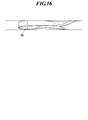
- FIG. 16 shows a state of the film optical waveguide 30i in which the twist phenomenon has occurred.
- the film optical waveguide 30i preferably has no angular misalignment. However, in the film optical waveguide 30i, due to an angle shift as shown in FIG. 15B, the start-up may be repeatedly disengaged at the time of sliding, and finally a twist phenomenon may occur as shown in FIG. there were.
- the phenomenon of angular misalignment and twist occurs because the rigidity of the optical waveguide is low, and there is a possibility that it may occur even in a slide configuration as described in Patent Document 2. If the rigidity of the film optical waveguide as a whole is increased by increasing the rigidity of the material, it is difficult to bend and slide the film optical waveguide in a narrow gap.
- An object of the present invention is to prevent the occurrence of a twisting phenomenon of a film optical waveguide due to a sliding operation of a sliding electronic device.
- the film optical waveguide according to the present invention is A film optical waveguide having a film-shaped optical waveguide portion composed of a core and a clad, and installed in a bent state in a slide mechanism portion of a sliding electronic device, A highly rigid and highly rigid portion including both end portions of the optical waveguide portion; And a low-rigidity low-rigidity part including a bent part of the optical waveguide part.
- the high-rigidity part includes a film bonded to the optical waveguide part.
- the film is bonded to at least one of the two surfaces of the optical waveguide portion.
- the ratio of the length of the film to the entire length of the optical waveguide portion is 54% or more.
- the high-rigidity part is formed of a material having a higher elastic modulus than the material of the low-rigidity part.
- the high-rigidity portion is thicker than the low-rigidity portion.
- the high-rigidity portion has a larger width in the optical axis direction than the low-rigidity portion.
- the film optical waveguide Comprising at least one film part, at least one of which is the optical waveguide part,
- the high rigidity portion is a portion where the two film portions are overlapped and fixed
- the low rigidity portion is a portion where the two film portions are overlapped and not fixed.
- the low-rigidity portion can facilitate the sliding operation of the sliding electronic device and the bending of the film optical waveguide, and the high-rigidity portion allows the film optical waveguide to slide by the sliding electronic device. It is possible to prevent the occurrence of twisting phenomenon.
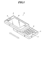
- FIG. 1 is a perspective view showing an external appearance of a sliding mobile phone according to a first embodiment of the present invention. It is a perspective view of the perspective direction which shows the structure of the slide mechanism part of 1st Embodiment. It is a side view which shows the structure of the slide mechanism part of 1st Embodiment seen from the Y direction of FIG. It is a graph which shows the relationship between the twist tolerance with respect to the sticking length of a film part, and the frequency
- FIG. 1 shows an external appearance of a sliding mobile phone 1 according to the present embodiment.
- the sliding mobile phone 1 includes an upper casing 2 and a lower casing 3.
- a display unit 4 and a speaker unit 5 are provided on the upper surface of the housing 2.
- An operation unit 6 and a microphone unit 7 are provided on the upper surface of the housing 3.
- the housing 2 can be slid with respect to the housing 3 in the arrow direction of FIG. By the sliding operation of the sliding mobile phone 1, the operation unit 6 and the microphone unit 7 of the housing 3 are exposed or stored.
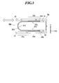
- FIG. 2 shows a perspective configuration of the slide mechanism portion 8a.
- FIG. 3 shows a configuration of the slide mechanism portion 8a viewed from the Y direction in FIG. 2 and 3, the X axis, the Y axis, and the Z axis are orthogonal to each other, and the same applies to the following drawings.
- the slide type mobile phone 1 includes a slide mechanism portion 8a therein.
- the slide mechanism unit 8a includes substrates 11 and 12, transmission / reception modules 21 and 22, and a film optical waveguide 30a.
- the substrate 11 is a circuit board provided inside the housing 2.
- the substrate 12 is a circuit board provided inside the housing 3.
- the transmission / reception module 21 is a module provided on the lower side of the substrate 11 to transmit / receive light.
- the transmission / reception module 22 is a module that is provided on the upper side of the substrate 12 and transmits / receives light.
- the film optical waveguide 30 a is a film-shaped optical waveguide having one end connected to the transmission / reception module 21 and the other end connected to the transmission / reception module 22.
- the light input from the transmission / reception module 21 is transmitted to the transmission / reception module 22 through one core of the film optical waveguide 30a.
- the light input from the transmission / reception module 22 is transmitted to the transmission / reception module 21 via the other core of the film optical waveguide 30a.
- the film optical waveguide 30a is bent and accommodated in a gap g between the substrates 11 and 12.
- the film optical waveguide 30a includes an optical waveguide portion 30A.
- the optical waveguide portion 30A has a bent portion 31A which is a portion bent in the state accommodated in the gap g, and non-bent portions 32A and 33A which are portions which are not bent in the state accommodated in the gap g. .
- optical waveguide parts are optical waveguide parts comprised from two cores which have translucency and light propagates, and the clad which has a refractive index different from the said core, and covers the said core, for example, , POW (Polymer Optical Waveguide).
- the material of the optical waveguide portion 30A is PET resin, acrylic or the like, and the material has a relatively low elastic modulus. For this reason, the optical waveguide portion 30A has a relatively low rigidity.
- the longitudinal direction of the optical waveguide portion 30A is the optical axis direction.
- the film optical waveguide 30a includes a film 34A attached to the non-bending portion 32A with an adhesive and a film 35A attached to the non-bending portion 33A.
- the film 34A is attached to the upper side (+ Z side) of the non-bent portion 32A on the transmission / reception module 21 side.
- the film 35A is attached to the lower side ( ⁇ Z side) of the non-bent portion 33A on the transmission / reception module 22 side.
- the widths of the films 34A and 35A (the length in the Y direction in FIG. 2) are the same as the widths of the non-bent portions 32A and 33A.
- the materials of the films 34A and 35A are PET resin, acrylic and the like, like the material of the optical waveguide portion 30A.
- the materials of the films 34A and 35A are materials having the same or different elastic modulus as that of the optical waveguide portion 30A.
- the portions where the films 34A and 35A are attached to the non-bent portions 32A and 33A are increased in thickness and have relatively high rigidity.
- one end portion of the film optical waveguide 30a that is, the film 34A and a portion where the film 34A is attached to the non-bent portion 32A, are defined as a highly rigid portion 32a.
- the length of the non-bent portion 32A ⁇ the length of the highly rigid portion 32a.
- the other end portion of the film optical waveguide 30a that is, the film 35A and a portion where the film 35A is attached to the non-bent portion 33A, are defined as a highly rigid portion 33a.
- portions other than the high-rigidity portions 32a and 33a in the film optical waveguide 30a include the bent portion 31A, have a relatively low rigidity, and serve as a low-rigidity portion 31a.
- the substrate 11 (housing 2) can be slid repeatedly with respect to the substrate 12 (housing 3) in the ⁇ X direction of FIG. During the sliding operation, the film optical waveguide 30a is deformed while being connected to the transmission / reception modules 21 and 22.
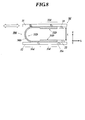
- FIG. 4 shows the relationship between the torsion resistance and the number of slides in which the torsion phenomenon occurs with respect to the length of the films 34A and 35A attached.
- the optical waveguide portion 30A was POW, and the materials of the films 34A and 35A were PET resin.
- the twist resistance of the film optical waveguide 30a is expressed by the following formula (1).
- b 1 thickness of the low rigidity portion 31a
- b 2 thickness of the high rigidity portions 32a and 33a
- l 1 length of the bending portion 31A
- l 2 length of the non-bending portions 32A and 33A
- l 3 length (attached) of the films 34A and 35A
- G 1 shear modulus of the low rigidity portion 31a
- G 2 shear modulus of the high rigidity portions 32a and 33a.
- l 1 , l 2 , and l 3 are lengths in the optical axis direction of the optical waveguide portion 30A.
- the pasting length [%] in FIG. 4 is represented by (l 3 / l 2 ).
- the twist resistance [times] is defined as the ratio (magnification) of the twist resistance of the film optical waveguide 30 a to the twist resistance of the optical waveguide portion 30 ⁇ / b> A (film optical waveguide without a film bonded).
- the number of slides was counted as one reciprocation of the slide in the X direction.
- produced was stopped to 100,000 times. Further, the film optical waveguide 30a was measured with an angle shift of 1 °.
- the twist resistance [times] of the film optical waveguide 30a increases as the pasting length [%] increases from 0% to 100% according to the equation (1). Further, according to the graph of FIG. 4, it was possible to achieve 100000 times or more of the number of slides in which the twist phenomenon occurs with respect to the twist resistance [times] of 1.8 times or more. In order to obtain 1.8 times or more of this twist resistance [times], the ratio of the length (l 3 ) of the films 34A and 35A to the total length of the optical waveguide portion 30A in the optical axis direction needs to be 54% or more. is there.
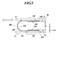
- FIG. 5 shows the configuration of the slide mechanism 8b.
- the slide mechanism portion 8b includes transmission / reception modules 21 and 22 and a film optical waveguide 30b between the substrates 11 and 12.
- the film optical waveguide 30b includes an optical waveguide portion 30B.
- the optical waveguide portion 30B has the same configuration as the optical waveguide portion 30A, and has a bent portion 31B and non-bent portions 32B and 33B.
- the film optical waveguide 30b includes a film 34B attached to the non-bending portion 32B with an adhesive and a film 35B attached to the non-bending portion 33B.
- the film 34B is attached to the lower side ( ⁇ Z side) of the non-bent portion 32B on the transmission / reception module 21 side.
- the film 35B is attached to the upper side (+ Z side) of the non-bent portion 33B on the transmission / reception module 22 side.
- the widths of the films 34B and 35B are the same as the widths of the non-bent portions 32B and 33B.
- the materials of the films 34B and 35B are the same as the materials of the films 34B and 35B.
- the film 34B and the portion where the film 34B is attached to the non-bent portion 32B are referred to as a highly rigid portion 32b.
- the length of the non-bent portion 32B ⁇ the length of the highly rigid portion 32b.
- the film 35B and the portion where the film 35B is attached to the non-bent portion 33B are referred to as a highly rigid portion 33b.
- the length of the non-bent portion 33B ⁇ the length of the highly rigid portion 33b.
- the part other than the high rigidity parts 32b and 33b in the film optical waveguide 30b be the low rigidity part 31b including the bending part 31B.
- the film optical waveguide 30a includes the low-rigidity portion 31a and the high-rigidity portions 32a and 33a in which the films 34A and 35A are attached to the non-bending portions 32A and 33A. Therefore, the sliding operation of the sliding mobile phone 1 and the bending of the film optical waveguide 30a can be facilitated by the low rigidity portion 31a, and the sliding operation of the sliding mobile phone 1 can be performed by the high rigidity portions 32a and 33a. It is possible to prevent the twisting phenomenon of the film optical waveguide 30a from occurring.
- the film optical waveguide 30b also has the same effect as the film optical waveguide 30a.
- FIG. 6 shows the configuration of the slide mechanism portion 8c.
- the apparatus configuration of the present embodiment has a configuration in which the slide mechanism unit 8a is replaced with the slide mechanism unit 8c in the slide type mobile phone 1 of the first embodiment.
- the slide mechanism portion 8 c includes transmission / reception modules 21 and 22 and a film optical waveguide 30 c between the substrates 11 and 12.
- the film optical waveguide 30c includes an optical waveguide portion 30C.
- the optical waveguide portion 30C includes a bent portion 31C and non-bent portions 32C and 33C.
- the longitudinal direction of the optical waveguide portion 30C is the optical axis direction.
- the film optical waveguide 30c has a high-rigidity portion 32c having a relatively high elastic modulus and a relatively high rigidity in a part of the material on the transmitting / receiving module 21 side in the non-bending portion 32C.
- the length of the non-bent portion 32C ⁇ the length of the highly rigid portion 32c.
- the film optical waveguide 30c has a high-rigidity portion 33c having a relatively high elastic modulus and a relatively high rigidity as a part of the material on the transmitting / receiving module 22 side in the non-bending portion 33C.
- the length of the non-bent portion 33C ⁇ the length of the highly rigid portion 33c.
- the width of the high-rigidity portions 32c and 33c (the length in the Y direction in FIG. 6) is the same as the width of the non-bending portions 32C and 33C.
- the portions other than the high-rigidity portions 32c and 33c in the film optical waveguide 30c include a bent portion 31C, which is a relatively low-rigidity portion, and this portion is referred to as a low-rigidity portion 31c.
- the core of the film optical waveguide 30c is disposed so as to straddle the high rigidity portions 32c and 33c.
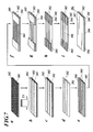
- an uncured core layer 302 is formed on the lower clad layer 301 by applying the material of the core layer 302.
- the material of the core layer 302 is assumed to be UV (Ultra Violet: UV) curable resin.
- the core layer 302 other than the core portion is masked with a resist or metal to form a mask 303, and the core layer 302 is irradiated with UV.
- the core portion is a portion that finally becomes the two cores of the film optical waveguide 30c.
- FIG. 7c only the core portion of the core layer 302 is cured.
- the mask 303 is removed, the uncured portion of the core layer 302 is removed by etching, and the core portion of the core layer 302 is formed.
- the material of the clad layer 304 is applied on the clad layer 301 other than the core layer 302.
- the material of the cladding layer 304 is a resin having a relatively high elastic modulus.
- masking is performed on the portions corresponding to the core portion and the high-rigidity portions 32c and 33c with a resist or metal to form a mask 305.
- the cladding layer 304 other than the mask 305 is removed by etching.
- the mask 305 is removed.
- the material of the cladding layer 306 is applied on the cladding layer 301 other than the core layer 302 and the cladding layer 304.
- the material of the clad layer 306 is a resin having a lower elastic modulus than the material of the clad layer 304.
- the clad layer 307 is apply
- the portion of the cladding layer 304 corresponds to the high rigidity portions 32c and 33c.
- the portion of the cladding layer 306 corresponds to the low rigidity portion 31c.
- the film optical waveguide 30c includes the low-rigidity portion 31c and the high-rigidity portions 32c and 33c made of a high-rigidity material. Therefore, the sliding operation of the sliding mobile phone 1 and the bending of the film optical waveguide 30c can be facilitated by the low rigidity portion 31c, and the sliding operation of the sliding mobile phone 1 can be performed by the high rigidity portions 32c and 33c. It is possible to prevent the twisting phenomenon of the film optical waveguide 30c due to the above.
- FIG. 8 shows the configuration of the slide mechanism 8d.
- the apparatus configuration of the present embodiment has a configuration in which the slide mechanism unit 8a is replaced with the slide mechanism unit 8d in the slide type mobile phone 1 of the first embodiment.
- the slide mechanism portion 8 d includes transmission / reception modules 21 and 22 and a film optical waveguide 30 d between the substrates 11 and 12.
- the film optical waveguide 30d includes an optical waveguide portion 30D.
- the optical waveguide portion 30D includes a bent portion 31D and non-bent portions 32D and 33D.
- the longitudinal direction of the optical waveguide portion 30D is the optical axis direction.
- the film optical waveguide 30d has a highly rigid portion 32d having a relatively large thickness and a part of the non-bent portion 32D on the transmission / reception module 21 side having a relatively large thickness.
- the length of the non-bent portion 32D ⁇ the length of the highly rigid portion 32d.
- the film optical waveguide 30d has a high-rigidity portion 33d having a relatively large and high rigidity at a part of the non-bent portion 33D on the transmission / reception module 22 side.
- the length of the non-bent portion 33D ⁇ the length of the highly rigid portion 33d.
- the portions other than the high-rigidity portions 32d and 33d in the film optical waveguide 30d include a bent portion 31D and are relatively low-rigidity portions, and this portion is referred to as a low-rigidity portion 31d.
- the core of the film optical waveguide 30d is disposed so as to straddle the highly rigid portions 32d and 33d.
- the film optical waveguide 30d includes the low-rigidity portion 31d and the high-rigidity portions 32d and 33d that are thicker than the low-rigidity portion 31d. Therefore, the sliding operation of the sliding mobile phone 1 and the bending of the film optical waveguide 30d can be facilitated by the low rigidity portion 31d, and the sliding operation of the sliding mobile phone 1 can be performed by the high rigidity portions 32d and 33d. It is possible to prevent the twisting phenomenon of the film optical waveguide 30d from occurring.
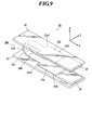
- FIG. 9 shows the configuration of the slide mechanism 8e.
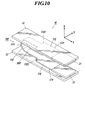
- FIG. 10 shows the configuration of the slide mechanism portion 8f.
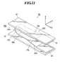
- FIG. 11 shows the configuration of the slide mechanism 8g.
- the apparatus configuration of the present embodiment has a configuration in which the slide mechanism unit 8a is replaced with the slide mechanism unit 8e in the slide type mobile phone 1 of the first embodiment.
- the slide mechanism portion 8 e includes transmission / reception modules 21 and 22 and a film optical waveguide 30 e between the substrates 11 and 12.
- the film optical waveguide 30e includes an optical waveguide portion 30E.
- the optical waveguide portion 30E includes a bent portion 31E and non-bent portions 32E and 33E.
- the film optical waveguide 30e has a high rigidity portion 32e having a relatively large and high rigidity with a partial width (width in the optical axis direction, length in the Y direction in FIG.
- the film optical waveguide 30e has a high-rigidity portion 33e having a relatively large and high rigidity at a part of the non-bent portion 33E on the transmission / reception module 22 side.
- the length of the non-bent portion 33E ⁇ the length of the highly rigid portion 33e.
- the portions other than the high-rigidity portions 32e and 33e in the film optical waveguide 30e include the bent portion 31E and are relatively low-rigidity portions, and the portion is referred to as a low-rigidity portion 31e.
- the widths of the high rigidity portions 32e and 33e are larger than the width of the low rigidity portion 31e.
- the end portion 32e1 of the high-rigidity portion 32e is an end portion on the low-rigidity portion 31e side and has a right-angle shape.
- the end portion 33e1 of the high-rigidity portion 33e is an end portion on the low-rigidity portion 31e side and has a right-angle shape.
- the core of the film optical waveguide 30e is disposed so as to straddle the high rigidity portions 32e and 33e.
- the slide mechanism 8e may be replaced with the slide mechanism 8f.
- the slide mechanism portion 8 f includes transmission / reception modules 21 and 22 and a film optical waveguide 30 f between the substrates 11 and 12.
- the film optical waveguide 30f includes an optical waveguide portion 30F.
- the optical waveguide portion 30F includes a bent portion 31F and non-bent portions 32F and 33F.
- the film optical waveguide 30f has a highly rigid portion 32f having a relatively large and high rigidity in a part of the non-bent portion 32F on the side of the transmitting / receiving module 21 (the length in the Y direction in FIG. 10).
- the length of the non-bent portion 32F ⁇ the length of the high-rigidity portion 32f.
- the film optical waveguide 30f has a highly rigid portion 33f having a relatively large and high rigidity at a part of the non-bent portion 33F on the transmission / reception module 22 side.
- the length of the non-bent portion 33F ⁇ the length of the highly rigid portion 33f.
- the portions other than the high-rigidity portions 32f and 33f in the film optical waveguide 30f include the bent portion 31F and are relatively low-rigidity portions, and this portion is referred to as a low-rigidity portion 31f.
- the widths of the high rigidity portions 32f and 33f are larger than the width of the low rigidity portion 31f.
- the end portion 32f1 of the high-rigidity portion 32f is an end portion on the low-rigidity portion 31f side, and has an R shape (circular shape).
- the end portion 33f1 of the high-rigidity portion 33f is an end portion on the low-rigidity portion 31f side, and has an R shape.
- the core of the film optical waveguide 30f is arranged so as to straddle the high rigidity portions 32f and 33f.
- the slide mechanism portion 8e may be replaced with the slide mechanism portion 8g.
- the slide mechanism 8g includes transmission / reception modules 21 and 22 and a film optical waveguide 30g between the substrates 11 and 12.
- the film optical waveguide 30g includes an optical waveguide portion 30G.
- the optical waveguide portion 30G includes a bent portion 31G and non-bent portions 32G and 33G.
- the film optical waveguide 30g has a highly rigid high-rigidity portion 32g having a relatively large width (a length in the Y direction in FIG. 11) on the transmission / reception module 21 side in the non-bending portion 32G.
- the film optical waveguide 30g has a high-rigidity portion 33g having a relatively large and high rigidity at a part of the non-bent portion 33G on the transmission / reception module 22 side.
- the length of the non-bent portion 33G ⁇ the length of the highly rigid portion 33g.
- the portions other than the high-rigidity portions 32g and 33g in the film optical waveguide 30g include the bent portion 31G and are relatively low-rigidity portions, and this portion is referred to as a low-rigidity portion 31g.
- the widths of the high rigidity portions 32g and 33g are larger than the width of the low rigidity portion 31g.
- the width of the high-rigidity portion 32g is gradually increased from the low-rigidity portion 31g side to the transmission / reception module 21 side.
- the width of the high-rigidity portion 33g gently increases from the low-rigidity portion 31g side to the transmission / reception module 22 side.
- the core of the film optical waveguide 30g is disposed so as to straddle the highly rigid portions 32g and 33g.
- a rectangular film-shaped optical waveguide portion 308 having a core and a clad is manufactured.
- the film waveguides 30e, 30f, and 30g are formed by removing the optical waveguide portion 308 by the mold 40.
- the mold 40 has a hole 40e for the film optical waveguide 30e, a hole 40f for the film optical waveguide 30f, and a hole 40g for the film optical waveguide 30g.
- the film optical waveguide 30e is formed by extracting the optical waveguide portion 308 through the hole 40e.
- the film optical waveguide 30f is formed by removing the optical waveguide portion 308 through the hole 40f.
- the film optical waveguide 30g is formed by removing the optical waveguide portion 308 through the hole 40g.
- the film optical waveguide 30e includes the low-rigidity portion 31e and the high-rigidity portions 32e and 33e having a width (the length in the short direction of the film optical waveguide 30e) larger than that of the low-rigidity portion 31e.
- the sliding operation of the sliding mobile phone 1 and the bending of the film optical waveguide 30e can be facilitated by the low rigidity portion 31e, and the sliding operation of the sliding mobile phone 1 can be performed by the high rigidity portions 32e and 33e. It is possible to prevent the twisting phenomenon of the film optical waveguide 30e from occurring.
- the film optical waveguides 30f and 30g have the same effect as the film optical waveguide 30e.
- FIG. 13 shows the configuration of the slide mechanism 8h.
- the apparatus configuration of the present embodiment has a configuration in which the slide mechanism unit 8a is replaced with the slide mechanism unit 8h in the slide type mobile phone 1 of the first embodiment.
- the slide mechanism 8 h includes transmission / reception modules 21 and 22 and a film optical waveguide 30 h between the substrates 11 and 12.
- the film optical waveguide 30h includes two film portions 30h1 and 30h2 that are overlapped.
- the film optical waveguide 30h includes a bent portion 31H and non-bent portions 32H and 33H.
- the film optical waveguide 30h has a high rigidity portion 32h which is a highly rigid portion in which a part of the film portions 30h1 and 30h2 on the transmission / reception module 21 side in the non-bending portion 32H is fixed by an adhesive.
- the film optical waveguide 30h includes a high-rigidity portion 33h that is a highly rigid portion to which a part of the film portions 30h1 and 30h2 on the transmission / reception module 22 side in the non-bending portion 33H is fixed.
- the length of the non-bent portion 33H ⁇ the length of the high-rigidity portion 33h.
- the portions other than the high-rigidity portions 32h and 33h in the film optical waveguide 30h where the film portions 30h1 and 30h2 are not fixed include the bent portion 31H, and are relatively low-rigidity portions. 31h. Since the film portions 30h1 and 30h2 are not fixed in the low-rigidity portion 31h, the bent portion 31H can have the minimum curvature.
- the widths of the high rigidity portions 32h and 33h are the same as the width of the low rigidity portion 31h.
- the film part 30h1 or the film part 30h2 may be configured as an optical waveguide part, and the film part 30h1 and the film part 30h2 may be configured as optical waveguide parts, respectively.
- the film optical waveguide 30h includes the low-rigidity portion 31h that is not fixed by overlapping the film portions 30h1 and 30h2, and the high-rigidity portion that is fixed by overlapping the film portions 30h1 and 30h2. 32h, 33h. Therefore, the sliding operation of the sliding mobile phone 1 and the bending of the film optical waveguide 30h can be facilitated by the low rigidity portion 31h, and the sliding operation of the sliding mobile phone 1 can be performed by the high rigidity portions 32h and 33h. It is possible to prevent the twisting phenomenon of the film optical waveguide 30h from occurring.
- each said embodiment is an example of the film optical waveguide which concerns on this invention, and is not limited to this.
- the slide type mobile phone 1 is used as the slide type electronic device.
- the present invention is not limited to this.
- another slide type electronic device such as PHS (Personal Handyphone System), PDA (Personal Digital Assistant), or a game machine may be used.
- the film is bonded to one surface of the optical waveguide portion.
- the present invention is not limited to this. It is good also as a structure by which the film was bonded together on both surfaces of the optical waveguide part.
- the film optical waveguide according to the present invention is suitable for a slide mechanism portion of a slide type electronic device.
Landscapes
- Physics & Mathematics (AREA)
- Engineering & Computer Science (AREA)
- Microelectronics & Electronic Packaging (AREA)
- General Physics & Mathematics (AREA)
- Optics & Photonics (AREA)
- Optical Integrated Circuits (AREA)
Abstract
スライド式電子機器のスライド動作によるフィルム光導波路のねじれ現象の発生を防ぐことである。 コア及びクラッドからなるフィルム状の光導波路部30Aを有し、スライド式電子機器のスライド機構部8aに屈曲した状態で設置されるフィルム光導波路30aは、光導波路部30Aの両端部分を含む高い剛性の高剛性部32a,33aと、光導波路部30Aの屈曲される部分を含む低い剛性の低剛性部31aと、を備える。
Description
本発明は、スライド式電子機器に収納されるフィルム光導波路に関する。
従来、スライド機構を有する携帯電話機等のスライド式電子機器が知られている。スライド式電子機器は、互いにスライド可能に係合された2つの筐体を有する。この2つの筐体を互いに並行にスライドさせることにより、操作部等が露出又は収納される。
スライド式電子機器の2つの筐体は、それぞれ回路基板が内蔵されている。スライド式電子機器の2つの回路基板は、導線を含むフレキシブルケーブルを介して互いに電気的に接続されている(例えば、特許文献1参照)。フレキシブルケーブルは、屈曲されて筺体内に収納される。フレキシブルケーブルは、スライド動作に応じて変形するため、スライド時にも電気的な接続が継続される。
また、スライド式電子機器のフレキシブルケーブルは、長年の使用によって、破断するおそれがあった。このため、フレキシブルケーブルの屈曲部の曲率を一定に保つガイド面を筺体内に設け、フレキシブルケーブルの破断を防ぐスライド式電子機器が考えられている(例えば、特許文献2参照)。
また、スライド式電子機器の2つの筐体の回路基板を、上記導線を含むフレキシブルケーブルに代えて、フィルム状の光導波路で接続する構成が知られている。ここで、図14A、図14Bを参照して、従来のスライド式電子機器のスライド機構部を説明する。図14Aに、スライド式電子機器のスライド前の状態におけるスライド機構部8iを示す。図14Bに、スライド式電子機器のスライド後の状態におけるスライド機構部8iを示す。
図14Aに示すように、スライド式電子機器のスライド機構部8iは、上側の筐体に設けられる基板11と、下側の筐体に設けられる基板12と、送受信モジュール21,22と、フィルム光導波路30iと、を備える。基板11,12は、互いに平行な位置に配置され、それらの間に、上下方向(図14AのZ方向)のギャップgを有する。基板11,12には、それぞれ、送受信モジュール21,22が設けられている。送受信モジュール21,22間には、フィルム光導波路30iが接続されている。フィルム光導波路30iは、コア及びクラッドから構成されているフィルム状の光導波路である。フィルム光導波路30iは、屈曲された状態でギャップgに収納されている。
スライド前のスライド式電子機器において、スライド部(図示略)(スライドレール等)のスライドにより、基板11を、-X方向にスライドすることが可能である。スライド式電子機器をスライドさせると、図14Bに示すように、基板11がスライドされ、フィルム光導波路30iは、送受信モジュール21,22と接続されたまま変形される。
スライド式電子機器のフィルム光導波路は、筐体内の狭いギャップ内に屈曲されて設けられる。このため、光導波路を破断することなくスライドさせるには、光導波路が低い剛性を有することが必要となる。
しかしながら、低剛性を実現するため低弾性率の材料で構成されている光導波路を用いても、光導波路実装時の角度ズレが発生するおそれがあった。図15Aに、角度ズレが無い(ズレの角度0°)フィルム光導波路30iの状態を示す。図15Bに、角度ズレが発生したフィルム光導波路30hの状態を示す。図16に、ねじれ現象が発生したフィルム光導波路30iの状態を示す。
フィルム光導波路30iは、図15Aに示すように、角度ズレの無い状態が好ましい。しかし、フィルム光導波路30iは、図15Bに示すような角度ズレ等が原因となり、スライド時において反復起動の外れが発生し、最終的に、図16に示すように、ねじれ現象が発生するおそれがあった。
角度ズレ、ねじれの現象は、光導波路の剛性が低いために発生しており、特許文献2に記載されるようなスライド構成であっても発生するおそれがあった。仮に、フィルム光導波路全体の材料を高弾性率にして剛性を高めた場合、狭ギャップでのフィルム光導波路の屈曲及びスライドが困難となっていた。
また、ねじれ現象が発生した際には、フィルム光導波路の伝播損失の増加や、ねじれ部位への応力による破断が発生するおそれがあった。更に、ねじれ現象が発生し、フィルム光導波路が2枚の基板のギャップで倒れた場合、フィルム光導波路の占めるスペースが増加する。このようにスペースが増加すると、実機にてフィルム光導波路が実装された場合、他の部品に接触して不具合を起こす可能性が高かった。
本発明の課題は、スライド式電子機器のスライド動作によるフィルム光導波路のねじれ現象の発生を防ぐことである。
上記課題を解決するため、本発明に係るフィルム光導波路は、
コア及びクラッドからなるフィルム形状の光導波路部を有し、スライド式電子機器のスライド機構部に屈曲した状態で設置されるフィルム光導波路であって、
前記光導波路部の両端部分を含む高い剛性の高剛性部と、
前記光導波路部の屈曲される部分を含む低い剛性の低剛性部と、を備える。
コア及びクラッドからなるフィルム形状の光導波路部を有し、スライド式電子機器のスライド機構部に屈曲した状態で設置されるフィルム光導波路であって、
前記光導波路部の両端部分を含む高い剛性の高剛性部と、
前記光導波路部の屈曲される部分を含む低い剛性の低剛性部と、を備える。
好ましくは、前記フィルム光導波路において、
前記高剛性部は、前記光導波路部に貼り合わせられたフィルムを備える。
前記高剛性部は、前記光導波路部に貼り合わせられたフィルムを備える。
好ましくは、前記フィルム光導波路において、
前記フィルムは、前記光導波路部の2つ面の少なくとも一方に貼り合わせられている。
前記フィルムは、前記光導波路部の2つ面の少なくとも一方に貼り合わせられている。
好ましくは、前記フィルム光導波路において、
前記光導波路部の光軸方向において、当該光導波路部の全長に対する前記フィルムの長さの割合は、54%以上である。
前記光導波路部の光軸方向において、当該光導波路部の全長に対する前記フィルムの長さの割合は、54%以上である。
好ましくは、前記フィルム光導波路において、
前記高剛性部は、前記低剛性部の材料よりも高い弾性率の材料で形成されている。
前記高剛性部は、前記低剛性部の材料よりも高い弾性率の材料で形成されている。
好ましくは、前記フィルム光導波路において、
前記高剛性部は、前記低剛性部よりも厚さが大きい。
前記高剛性部は、前記低剛性部よりも厚さが大きい。
好ましくは、前記フィルム光導波路において、
前記高剛性部は、前記低剛性部よりも光軸方向の幅が大きい。
前記高剛性部は、前記低剛性部よりも光軸方向の幅が大きい。
好ましくは、前記フィルム光導波路において、
少なくとも1枚が前記光導波路部である2枚のフィルム部を備え、
前記高剛性部は、前記2枚のフィルム部が重ね合わせられて固着された部分であり、
前記低剛性部は、前記2枚のフィルム部が重ね合わせられて固着されていない部分である。
少なくとも1枚が前記光導波路部である2枚のフィルム部を備え、
前記高剛性部は、前記2枚のフィルム部が重ね合わせられて固着された部分であり、
前記低剛性部は、前記2枚のフィルム部が重ね合わせられて固着されていない部分である。
本発明によれば、低剛性部により、スライド式電子機器のスライド動作とフィルム光導波路の屈曲とを容易にすることができるとともに、高剛性部により、スライド式電子機器のスライド動作によるフィルム光導波路のねじれ現象の発生を防ぐことができる。
以下、添付図面を参照して本発明に係る実施の第1~第5の形態を順に詳細に説明する。ただし、発明の範囲は、図示例に限定されない。
(第1の実施の形態)
図1~図5を参照して、本発明に係る実施の第1の形態を詳細に説明する。図1に、本実施の形態のスライド式携帯電話機1の外観を示す。
図1~図5を参照して、本発明に係る実施の第1の形態を詳細に説明する。図1に、本実施の形態のスライド式携帯電話機1の外観を示す。
図1に示すように、本実施の形態のスライド式携帯電話機1は、上側の筐体2と、下側の筐体3と、を備える。筐体2の上面には、表示部4と、スピーカ部5と、が設けられている。筐体3の上面には、操作部6と、マイク部7と、が設けられている。
筐体2は、筐体3に対して、上面の向きを上に保ったまま、図1の矢印方向にスライドさせることが可能である。スライド式携帯電話機1のスライド動作により、筐体3の操作部6及びマイク部7が、露出又は収納される。
図2及び図3を参照して、スライド式携帯電話機1のスライド機構部8aの構成を説明する。図2に、スライド機構部8aの斜視構成を示す。図3に、図2のY方向から見たスライド機構部8aの構成を示す。また、図2、図3において、X軸、Y軸、Z軸は互いに直交しているものとし、以下の図でも同様とする。
図2及び図3に示すように、スライド式携帯電話機1は、内部に、スライド機構部8aを備える。スライド機構部8aは、基板11,12と、送受信モジュール21,22と、フィルム光導波路30aと、を備える。
基板11は、筐体2内部に設けられる回路基板である。基板12は、筐体3内部に設けられる回路基板である。送受信モジュール21は、基板11の下側に設けられ、光を送受信するモジュールである。送受信モジュール22は、基板12の上側に設けられ、光を送受信するモジュールである。フィルム光導波路30aは、一端が送受信モジュール21に接続され、他端が送受信モジュール22に接続されたフィルム形状の光導波路である。
つまり、送受信モジュール21から入力される光が、フィルム光導波路30aの一方のコアを介して、送受信モジュール22に伝送される。あるいは、送受信モジュール22から入力される光が、フィルム光導波路30aのもう一方のコアを介して、送受信モジュール21に伝送される。
フィルム光導波路30aは、基板11,12間のギャップgに屈曲されて収納されている。フィルム光導波路30aは、光導波路部30Aを備える。光導波路部30Aは、ギャップgに収納された状態で屈曲された部分である屈曲部31Aと、ギャップgに収納された状態で屈曲されていない部分である非屈曲部32A,33Aと、を有する。
光導波路部30Aは、透光性を有し光が伝播される2本のコアと、当該コアと異なる屈折率を有し当該コアを覆うクラッドと、から構成される光導波路部であり、例えば、POW(Polymer Optical Waveguide)である。光導波路部30Aの材料は、PET樹脂、アクリル等であり、その材質が比較的低弾性率である。このため、光導波路部30Aは、比較的低い剛性を有する。光導波路部30Aの長手方向を光軸方向とする。
また、フィルム光導波路30aは、接着剤により非屈曲部32Aに貼り付けられたフィルム34Aと、同じく非屈曲部33Aに貼り付けられたフィルム35Aと、を有する。フィルム34Aは、送受信モジュール21側で非屈曲部32Aの上側(+Z側)に貼り付けられている。フィルム35Aは、送受信モジュール22側で非屈曲部33Aの下側(-Z側)に貼り付けられている。フィルム34A,35Aの幅(図2におけるY方向の長さ)は、非屈曲部32A,33Aの幅と同じである。フィルム34A,35Aの材料は、光導波路部30Aの材料と同様に、PET樹脂、アクリル等である。また、フィルム34A,35Aの材料は、光導波路部30Aと同じ又は異なる弾性率の材料である。
非屈曲部32A,33Aにおけるフィルム34A,35Aの貼り付け部分は、厚みが増加されており、比較的高い剛性を有する。ここで、図2及び図3に示すように、フィルム光導波路30aの一端部分であって、フィルム34Aと、非屈曲部32Aにおけるフィルム34Aの貼り付け部分とを、高剛性部32aとする。光導波路部30Aの光軸方向において、非屈曲部32Aの長さ≧高剛性部32aの長さである。同じくフィルム光導波路30aの他の一端部分であって、フィルム35Aと、非屈曲部33Aにおけるフィルム35Aの貼り付け部分とを、高剛性部33aとする。光導波路部30Aの光軸方向において、非屈曲部33Aの長さ≧高剛性部33aの長さである。また、フィルム光導波路30aにおける高剛性部32a,33a以外の部分は、屈曲部31Aを含み、比較的低い剛性を有し、低剛性部31aとする。
基板11(筐体2)は、基板12(筐体3)に対して、図2の±X方向に反復してスライド可能である。このスライド動作時に、フィルム光導波路30aは、送受信モジュール21,22と接続されたまま、変形される。
次いで、図4を参照して、フィルム光導波路30aのスライド動作に関する実験例を説明する。図4に、フィルム34A,35Aの貼り付け長に対する、ねじれ耐性と、ねじれ現象が発生したスライド回数との関係を示す。
この実験では、光導波路部30AをPOWとし、フィルム34A,35Aの材料をPET樹脂とした。フィルム光導波路30aのねじれ耐性は、次式(1)で表される。

但し、b1:低剛性部31aの厚さ、b2:高剛性部32a,33aの厚さ、l1:屈曲部31Aの長さ、l2:非屈曲部32A,33Aの長さ、l3:フィルム34A,35Aの(貼り付け)長さ、G1:低剛性部31aのせん断弾性率、G2:高剛性部32a,33aのせん断弾性率、である。また、l1,l2,l3は、光導波路部30Aの光軸方向における長さである。
図4における貼り付け長[%]は、(l3/l2)で表される。また、図4において、ねじれ耐性[倍]は、光導波路部30A(フィルムを貼り合わせていないフィルム光導波路)のねじれ耐性に対するフィルム光導波路30aのねじれ耐性の割合(倍率)とした。また、スライド回数とは、図2において、X方向のスライドの1往復を1回とカウントした。また、ねじれ現象が発生するまでのスライド回数の測定を、100000回まで行って停止した。また、フィルム光導波路30aに角度ズレ1°を付けて測定を行った。
図4のグラフによると、フィルム光導波路30aのねじれ耐性[倍]は、式(1)に応じて貼り付け長[%]が0%から100%まで大きくなるにつれて、増加していく。また、図4のグラフによると、ねじれ耐性[倍]を1.8倍以上にさせたものに対しては、ねじれ現象が発生するスライド回数について、100000回以上を達成することができた。このねじれ耐性[倍]の1.8倍以上を得るには、光軸方向について、光導波路部30Aの全長に対するフィルム34A,35Aの長さ(l3)の割合を54%以上にする必要がある。
また、図5に示すように、スライド機構部8aに代えて、スライド機構部8bを用いる構成としてもよい。図5に、スライド機構部8bの構成を示す。
スライド機構部8bは、基板11,12間に、送受信モジュール21,22と、フィルム光導波路30bとを有する。フィルム光導波路30bは、光導波路部30Bを備える。光導波路部30Bは、光導波路部30Aと同様の構成を有し、屈曲部31B及び非屈曲部32B,33Bを有する。また、フィルム光導波路30bは、接着剤により非屈曲部32Bに貼り付けられたフィルム34Bと、同じく非屈曲部33Bに貼り付けられたフィルム35Bと、を有する。フィルム34Bは、送受信モジュール21側で非屈曲部32Bの下側(-Z側)に貼り付けられている。フィルム35Bは、送受信モジュール22側で非屈曲部33Bの上側(+Z側)に貼り付けられている。フィルム34B,35Bの幅(図2におけるY方向の長さ)は、非屈曲部32B,33Bの幅と同じである。フィルム34B,35Bの材料は、フィルム34B,35Bの材料と同様である。
フィルム光導波路30bのうち、フィルム34Bと、非屈曲部32Bにおけるフィルム34Bの貼り付け部分とを、高剛性部32bとする。光導波路部30Bの光軸方向において、非屈曲部32Bの長さ≧高剛性部32bの長さである。同じくフィルム35Bと、非屈曲部33Bにおけるフィルム35Bの貼り付け部分とを、高剛性部33bとする。光導波路部30Bの光軸方向において、非屈曲部33Bの長さ≧高剛性部33bの長さである。また、フィルム光導波路30bにおける高剛性部32b,33b以外の部分を、屈曲部31Bを含む低剛性部31bとする。
以上、本実施の形態によれば、フィルム光導波路30aは、低剛性部31aと、非屈曲部32A,33Aにフィルム34A,35Aが貼り付けられた高剛性部32a,33aとを備える。このため、低剛性部31aにより、スライド式携帯電話機1のスライド動作とフィルム光導波路30aの屈曲とを容易にすることができるとともに、高剛性部32a,33aにより、スライド式携帯電話機1のスライド動作によるフィルム光導波路30aのねじれ現象の発生を防ぐことができる。
また、光導波路部30Aの光軸方向における全長に対するフィルム34A,35Aの長さの割合を54%以上にすることで、より大きなスライド回数に対してもスライド式携帯電話機1のスライド動作によるフィルム光導波路30aのねじれ現象の発生を防ぐことができる。フィルム光導波路30bも、フィルム光導波路30aと同様の効果を奏する。
(第2の実施の形態)
図6及び図7を参照して、本発明に係る第2の実施の形態を説明する。図6に、スライド機構部8cの構成を示す。
図6及び図7を参照して、本発明に係る第2の実施の形態を説明する。図6に、スライド機構部8cの構成を示す。
本実施の形態の装置構成は、第1の実施の形態のスライド式携帯電話機1において、スライド機構部8aを、スライド機構部8cに代えた構成を有する。図6に示すように、スライド機構部8cは、基板11,12間に、送受信モジュール21,22と、フィルム光導波路30cとを有する。フィルム光導波路30cは、光導波路部30Cを備える。光導波路部30Cは、屈曲部31C、非屈曲部32C,33Cを備える。光導波路部30Cの長手方向を光軸方向とする。また、フィルム光導波路30cは、非屈曲部32Cにおける送受信モジュール21側の一部の材質が比較的高い弾性率であり比較的高い剛性の高剛性部32cを有する。光導波路部30Cの光軸方向において、非屈曲部32Cの長さ≧高剛性部32cの長さである。同じくフィルム光導波路30cは、非屈曲部33Cにおける送受信モジュール22側の一部の材質が比較的高い弾性率であり比較的高い剛性の高剛性部33cを有する。光導波路部30Cの光軸方向において、非屈曲部33Cの長さ≧高剛性部33cの長さである。
高剛性部32c,33cの幅(図6におけるY方向の長さ)は、非屈曲部32C,33Cの幅と同じである。また、フィルム光導波路30cにおける高剛性部32c,33c以外の部分は、屈曲部31Cを含み、比較的低い剛性の部分であり、当該部分を低剛性部31cとする。フィルム光導波路30cのコアは、高剛性部32c,33cを跨るように配置されている。
次いで、図7を参照して、フィルム光導波路30cの製造方法を説明する。図7に、フィルム光導波路30c製造の各工程の状態を示す。
先ず、図7のaに示すように、下側のクラッド層301の上に、コア層302の材料が塗布されることにより未硬化のコア層302が形成される。コア層302の材料は、UV(Ultra Violet:紫外線)硬化樹脂であるものとする。そして、図7のbに示すように、レジスト又はメタルでコア部分以外のコア層302に対するマスキングがなされてマスク303が形成され、コア層302にUVが照射される。コア部分とは、最終的にフィルム光導波路30cの2本のコアとなる部分である。そして、図7のcに示すように、コア層302のコア部分のみが硬化される。
そして、図7のdに示すように、マスク303が除去され、エッチングによりコア層302の未硬化部分が除去され、コア層302のコア部分が形成される。そして、図7のeに示すように、コア層302以外のクラッド層301の上にクラッド層304の材料が塗布される。クラッド層304の材料は、比較的高弾性率の樹脂である。そして、図7のfに示すように、レジスト又はメタルで、コア部分及び高剛性部32c,33cに対応する部分に対するマスキングがなされてマスク305が形成される。
そして、図7のgに示すように、エッチングによりマスク305以外のクラッド層304が除去される。そして、図7のhに示すように、マスク305が除去される。そして、図7のiに示すように、コア層302及びクラッド層304以外のクラッド層301の上にクラッド層306の材料が塗布される。クラッド層306の材料は、クラッド層304の材料に比べて低弾性率の樹脂である。そして、図7のjに示すように、コア層302、クラッド層304及びクラッド層306の上にクラッド層307が塗布されて、フィルム光導波路30cが完成する。クラッド層304の部分は、高剛性部32c,33cに対応する。クラッド層306の部分は、低剛性部31cに対応する。
以上、本実施の形態によれば、フィルム光導波路30cは、低剛性部31cと、高剛性の材質の高剛性部32c,33cとを備える。このため、低剛性部31cにより、スライド式携帯電話機1のスライド動作とフィルム光導波路30cの屈曲とを容易にすることができるとともに、高剛性部32c,33cにより、スライド式携帯電話機1のスライド動作によるフィルム光導波路30cのねじれ現象の発生を防ぐことができる。
(第3の実施の形態)
図8を参照して、本発明に係る第3の実施の形態を説明する。図8に、スライド機構部8dの構成を示す。
図8を参照して、本発明に係る第3の実施の形態を説明する。図8に、スライド機構部8dの構成を示す。
本実施の形態の装置構成は、第1の実施の形態のスライド式携帯電話機1において、スライド機構部8aを、スライド機構部8dに代えた構成を有する。図8に示すように、スライド機構部8dは、基板11,12間に、送受信モジュール21,22と、フィルム光導波路30dとを有する。フィルム光導波路30dは、光導波路部30Dを備える。光導波路部30Dは、屈曲部31D、非屈曲部32D,33Dを備える。光導波路部30Dの長手方向を光軸方向とする。また、フィルム光導波路30dは、非屈曲部32Dにおける送受信モジュール21側の一部の厚さが比較的大きく高い剛性の高剛性部32dを有する。光導波路部30Dの光軸方向において、非屈曲部32Dの長さ≧高剛性部32dの長さである。同じくフィルム光導波路30dは、非屈曲部33Dにおける送受信モジュール22側の一部の厚さが比較的大きく高い剛性の高剛性部33dを有する。光導波路部30Dの光軸方向において、非屈曲部33Dの長さ≧高剛性部33dの長さである。
フィルム光導波路30dにおける高剛性部32d,33d以外の部分は、屈曲部31Dを含み、比較的低い剛性の部分であり、当該部分を低剛性部31dとする。フィルム光導波路30dのコアは、高剛性部32d,33dを跨るように配置されている。
以上、本実施の形態によれば、フィルム光導波路30dは、低剛性部31dと、低剛性部31dよりも厚さが大きい高剛性部32d,33dとを備える。このため、低剛性部31dにより、スライド式携帯電話機1のスライド動作とフィルム光導波路30dの屈曲とを容易にすることができるとともに、高剛性部32d,33dにより、スライド式携帯電話機1のスライド動作によるフィルム光導波路30dのねじれ現象の発生を防ぐことができる。
(第4の実施の形態)
図9~図12を参照して、本発明に係る第4の実施の形態を説明する。図9に、スライド機構部8eの構成を示す。図10に、スライド機構部8fの構成を示す。図11に、スライド機構部8gの構成を示す。
図9~図12を参照して、本発明に係る第4の実施の形態を説明する。図9に、スライド機構部8eの構成を示す。図10に、スライド機構部8fの構成を示す。図11に、スライド機構部8gの構成を示す。
本実施の形態の装置構成は、第1の実施の形態のスライド式携帯電話機1において、スライド機構部8aを、スライド機構部8eに代えた構成を有する。図9に示すように、スライド機構部8eは、基板11,12間に、送受信モジュール21,22と、フィルム光導波路30eとを有する。フィルム光導波路30eは、光導波路部30Eを備える。光導波路部30Eは、屈曲部31E、非屈曲部32E,33Eを備える。また、フィルム光導波路30eは、非屈曲部32Eにおける送受信モジュール21側の一部の幅(光軸方向の幅、図9におけるY方向の長さ)が比較的大きく高い剛性の高剛性部32eを有する。光導波路部30Eの光軸方向において、非屈曲部32Eの長さ≧高剛性部32eの長さである。同じくフィルム光導波路30eは、非屈曲部33Eにおける送受信モジュール22側の一部の幅が比較的大きく高い剛性の高剛性部33eを有する。光導波路部30Eの光軸方向において、非屈曲部33Eの長さ≧高剛性部33eの長さである。
フィルム光導波路30eにおける高剛性部32e,33e以外の部分は、屈曲部31Eを含み、比較的低い剛性の部分であり、当該部分を低剛性部31eとする。高剛性部32e,33eの幅は、低剛性部31eの幅よりも大きい。また、高剛性部32eの端部32e1は、低剛性部31e側の端部であり、直角形状を有する。同じく高剛性部33eの端部33e1は、低剛性部31e側の端部であり、直角形状を有する。フィルム光導波路30eのコアは、高剛性部32e,33eを跨るように配置されている。
また、スライド機構部8eを、スライド機構部8fに代えた構成としてもよい。図10に示すように、スライド機構部8fは、基板11,12間に、送受信モジュール21,22と、フィルム光導波路30fとを有する。フィルム光導波路30fは、光導波路部30Fを備える。光導波路部30Fは、屈曲部31F、非屈曲部32F,33Fを備える。また、フィルム光導波路30fは、非屈曲部32Fにおける送受信モジュール21側の一部の幅(図10におけるY方向の長さ)が比較的大きく高い剛性の高剛性部32fを有する。光導波路部30Fの光軸方向において、非屈曲部32Fの長さ≧高剛性部32fの長さである。同じくフィルム光導波路30fは、非屈曲部33Fにおける送受信モジュール22側の一部の幅が比較的大きく高い剛性の高剛性部33fを有する。光導波路部30Fの光軸方向において、非屈曲部33Fの長さ≧高剛性部33fの長さである。
フィルム光導波路30fにおける高剛性部32f,33f以外の部分は、屈曲部31Fを含み、比較的低い剛性の部分であり、当該部分を低剛性部31fとする。高剛性部32f,33fの幅は、低剛性部31fの幅よりも大きい。また、高剛性部32fの端部32f1は、低剛性部31f側の端部であり、R形状(円形状)を有する。同じく高剛性部33fの端部33f1は、低剛性部31f側の端部であり、R形状を有する。フィルム光導波路30fのコアは、高剛性部32f,33fを跨るように配置されている。
また、スライド機構部8eを、スライド機構部8gに代えた構成としてもよい。図11に示すように、スライド機構部8gは、基板11,12間に、送受信モジュール21,22と、フィルム光導波路30gとを有する。フィルム光導波路30gは、光導波路部30Gを備える。光導波路部30Gは、屈曲部31G、非屈曲部32G,33Gを備える。また、フィルム光導波路30gは、非屈曲部32Gにおける送受信モジュール21側の一部の幅(図11におけるY方向の長さ)が比較的大きく高い剛性の高剛性部32gを有する。光導波路部30Gの光軸方向において、非屈曲部32Gの長さ≧高剛性部32gの長さである。同じくフィルム光導波路30gは、非屈曲部33Gにおける送受信モジュール22側の一部の幅が比較的大きく高い剛性の高剛性部33gを有する。光導波路部30Gの光軸方向において、非屈曲部33Gの長さ≧高剛性部33gの長さである。
フィルム光導波路30gにおける高剛性部32g,33g以外の部分は、屈曲部31Gを含み、比較的低い剛性の部分であり、当該部分を低剛性部31gとする。高剛性部32g,33gの幅は、低剛性部31gの幅よりも大きい。また、高剛性部32gは、低剛性部31g側から送受信モジュール21側へなだらかに幅が増加している。同じく高剛性部33gは、低剛性部31g側から送受信モジュール22側へなだらかに幅が増加している。フィルム光導波路30gのコアは、高剛性部32g,33gを跨るように配置されている。
次いで、図12を参照して、フィルム光導波路30e,30f,30gの製造方法を説明する。図12に、フィルム光導波路30e,30f,30g製造の工程の状態を示す。
図12に示すように、先ず、コア及びクラッドを有する矩形フィルム形状の光導波路部308を製造する。そして、型40により、光導波路部308を抜くことで、フィルム光導波路30e,30f,30gが形成される。型40は、フィルム光導波路30e用の穴部40eと、フィルム光導波路30f用の穴部40fと、フィルム光導波路30g用の穴部40gと、を有する。具体的には、光導波路部308を穴部40eで抜くことでフィルム光導波路30eが形成される。また、光導波路部308を穴部40fで抜くことでフィルム光導波路30fが形成される。また、光導波路部308を穴部40gで抜くことでフィルム光導波路30gが形成される。
以上、本実施の形態によれば、フィルム光導波路30eは、低剛性部31eと、低剛性部31eよりも幅(フィルム光導波路30eの短手方向の長さ)が大きい高剛性部32e,33eとを備える。このため、低剛性部31eにより、スライド式携帯電話機1のスライド動作とフィルム光導波路30eの屈曲とを容易にすることができるとともに、高剛性部32e,33eにより、スライド式携帯電話機1のスライド動作によるフィルム光導波路30eのねじれ現象の発生を防ぐことができる。フィルム光導波路30f,30gは、フィルム光導波路30eと同様の効果を奏する。
(第5の実施の形態)
図13を参照して、本発明に係る第5の実施の形態を説明する。図13に、スライド機構部8hの構成を示す。
図13を参照して、本発明に係る第5の実施の形態を説明する。図13に、スライド機構部8hの構成を示す。
本実施の形態の装置構成は、第1の実施の形態のスライド式携帯電話機1において、スライド機構部8aを、スライド機構部8hに代えた構成を有する。図13に示すように、スライド機構部8hは、基板11,12間に、送受信モジュール21,22と、フィルム光導波路30hとを有する。フィルム光導波路30hは、2枚のフィルム部30h1,30h2を重ね合わせて備える。フィルム光導波路30hは、屈曲部31H、非屈曲部32H,33Hを備える。また、フィルム光導波路30hは、非屈曲部32Hにおける送受信モジュール21側の一部のフィルム部30h1,30h2が接着剤により固着された高い剛性の部分である高剛性部32hを有する。フィルム光導波路30hの光導波路部(コア及びクラッド)の光軸方向において、非屈曲部32Hの長さ≧高剛性部32hの長さである。同じくフィルム光導波路30hは、非屈曲部33Hにおける送受信モジュール22側の一部のフィルム部30h1,30h2が固着された高い剛性の部分である高剛性部33hを有する。フィルム光導波路30hの光導波路部の光軸方向において、非屈曲部33Hの長さ≧高剛性部33hの長さである。
また、フィルム光導波路30hにおける高剛性部32h,33h以外の、フィルム部30h1,30h2が固着されていない部分は、屈曲部31Hを含み、比較的低い剛性の部分であり、当該部分を低剛性部31hとする。低剛性部31hにおいて、フィルム部30h1,30h2が固着されていないため、屈曲部31Hは、最小の曲率をとることができる。高剛性部32h,33hの幅は、低剛性部31hの幅と同じである。また、フィルム部30h1又はフィルム部30h2が、光導波路部である構成としてもよく、フィルム部30h1及びフィルム部30h2が、それぞれ光導波路部である構成としてもよい。
以上、本実施の形態によれば、フィルム光導波路30hは、フィルム部30h1,30h2を重ね合わせて固着されていない低剛性部31hと、フィルム部30h1,30h2を重ね合わせて固着された高剛性部32h,33hとを備える。このため、低剛性部31hにより、スライド式携帯電話機1のスライド動作とフィルム光導波路30hの屈曲とを容易にすることができるとともに、高剛性部32h,33hにより、スライド式携帯電話機1のスライド動作によるフィルム光導波路30hのねじれ現象の発生を防ぐことができる。
なお、上記各実施の形態における記述は、本発明に係るフィルム光導波路の一例であり、これに限定されるものではない。
例えば、上記各実施の形態の構成の少なくとも2つを組み合わせることとしてもよい。
また、上記実施の形態では、スライド式電子機器として、スライド式携帯電話機1を用いる構成としたが、これに限定されるものではない。例えば、PHS(Personal Handyphone System)、PDA(Personal Digital Assistant)、ゲーム機等、他のスライド式電子機器を用いる構成としてもよい。
また、上記第1の実施の形態では、フィルムが光導波路部の片面に貼り合わされた構成としたが、これに限定されるものではない。フィルムが光導波路部の両面に貼り合わされた構成としてもよい。
その他、上記各実施の形態におけるフィルム光導波路の細部構成及び詳細動作に関しても、本発明の趣旨を逸脱しない範囲で適宜変更可能である。
以上のように、本発明に係るフィルム光導波路は、スライド式電子機器のスライド機構部に適している。
1 スライド式携帯電話機
2,3 筐体
4 表示部
5 スピーカ部
6 操作部
7 マイク部
8a,8b,8c,8d,8e,8f,8g,8h,8i スライド機構部
11,12 基板
21,22 送受信モジュール
g ギャップ
30a,30b,30c,30d,30e,30f,30g,30h,30i フィルム光導波路
30A,30B,30C,30D,30E,30F,30G 光導波路部
31A,31B,31C,31D,31E,31F,31G,31H 屈曲部
32A,33A,32B,33B,32C,33C,32D,33D,32E,33E,32F,33F,32G,33G,32H,33H 非屈曲部
34A,35A,34B,35B フィルム
31a,31b,31c,31d,31e,31f,31g,31h 低剛性部
32a,33a,32b,33b,32c,33c,32d,33d,32e,33e,32f,33f,32g,33g,32h,33h 高剛性部
301,304,306,307 クラッド層
302 コア層
303,305 マスク
32e1,33e1 端部
308 光導波路部
40 型
40e,40f,40g 穴部
30h1,30h2 フィルム部
2,3 筐体
4 表示部
5 スピーカ部
6 操作部
7 マイク部
8a,8b,8c,8d,8e,8f,8g,8h,8i スライド機構部
11,12 基板
21,22 送受信モジュール
g ギャップ
30a,30b,30c,30d,30e,30f,30g,30h,30i フィルム光導波路
30A,30B,30C,30D,30E,30F,30G 光導波路部
31A,31B,31C,31D,31E,31F,31G,31H 屈曲部
32A,33A,32B,33B,32C,33C,32D,33D,32E,33E,32F,33F,32G,33G,32H,33H 非屈曲部
34A,35A,34B,35B フィルム
31a,31b,31c,31d,31e,31f,31g,31h 低剛性部
32a,33a,32b,33b,32c,33c,32d,33d,32e,33e,32f,33f,32g,33g,32h,33h 高剛性部
301,304,306,307 クラッド層
302 コア層
303,305 マスク
32e1,33e1 端部
308 光導波路部
40 型
40e,40f,40g 穴部
30h1,30h2 フィルム部
Claims (8)
- コア及びクラッドからなるフィルム形状の光導波路部を有し、スライド式電子機器のスライド機構部に屈曲した状態で設置されるフィルム光導波路であって、
前記光導波路部の両端部分を含む高い剛性の高剛性部と、
前記光導波路部の屈曲される部分を含む低い剛性の低剛性部と、を備えるフィルム光導波路。 - 前記高剛性部は、前記光導波路部に貼り合わせられたフィルムを備える請求項1に記載のフィルム光導波路。
- 前記フィルムは、前記光導波路部の2つ面の少なくとも一方に貼り合わせられている請求項2に記載のフィルム光導波路。
- 前記光導波路部の光軸方向において、当該光導波路部の全長に対する前記フィルムの長さの割合は、54%以上である請求項2又は3に記載のフィルム光導波路。
- 前記高剛性部は、前記低剛性部の材料よりも高い弾性率の材料で形成されている請求項1に記載のフィルム光導波路。
- 前記高剛性部は、前記低剛性部よりも厚さが大きい請求項1に記載のフィルム光導波路。
- 前記高剛性部は、前記低剛性部よりも光軸方向の幅が大きい請求項1に記載のフィルム光導波路。
- 少なくとも1枚が前記光導波路部である2枚のフィルム部を備え、
前記高剛性部は、前記2枚のフィルム部が重ね合わせられて固着された部分であり、
前記低剛性部は、前記2枚のフィルム部が重ね合わせられて固着されていない部分である請求項1に記載のフィルム光導波路。
Applications Claiming Priority (2)
| Application Number | Priority Date | Filing Date | Title |
|---|---|---|---|
| JP2009053137A JP2010204609A (ja) | 2009-03-06 | 2009-03-06 | フィルム光導波路 |
| JP2009-053137 | 2009-03-06 |
Publications (1)
| Publication Number | Publication Date |
|---|---|
| WO2010101201A1 true WO2010101201A1 (ja) | 2010-09-10 |
Family
ID=42709755
Family Applications (1)
| Application Number | Title | Priority Date | Filing Date |
|---|---|---|---|
| PCT/JP2010/053492 Ceased WO2010101201A1 (ja) | 2009-03-06 | 2010-03-04 | フィルム光導波路 |
Country Status (2)
| Country | Link |
|---|---|
| JP (1) | JP2010204609A (ja) |
| WO (1) | WO2010101201A1 (ja) |
Citations (6)
| Publication number | Priority date | Publication date | Assignee | Title |
|---|---|---|---|---|
| JP2006023661A (ja) * | 2004-07-09 | 2006-01-26 | Omron Corp | フィルム光導波路及びその製造方法並びにフィルム光導波路用基材 |
| JP2006042307A (ja) * | 2004-03-12 | 2006-02-09 | Matsushita Electric Ind Co Ltd | 携帯機器 |
| WO2006035633A1 (ja) * | 2004-09-27 | 2006-04-06 | Nec Corporation | 光信号入出力機構を有する半導体装置 |
| WO2007004575A1 (ja) * | 2005-06-30 | 2007-01-11 | Mitsui Chemicals, Inc. | 光導波路フィルムおよび光電気混載フィルム |
| JP2007033830A (ja) * | 2005-07-26 | 2007-02-08 | Fuji Xerox Co Ltd | フレキシブル光導波路 |
| WO2007132751A1 (ja) * | 2006-05-12 | 2007-11-22 | Mitsui Chemicals, Inc. | 光電気混載フィルムおよびそれを収納した電子機器 |
-
2009
- 2009-03-06 JP JP2009053137A patent/JP2010204609A/ja active Pending
-
2010
- 2010-03-04 WO PCT/JP2010/053492 patent/WO2010101201A1/ja not_active Ceased
Patent Citations (6)
| Publication number | Priority date | Publication date | Assignee | Title |
|---|---|---|---|---|
| JP2006042307A (ja) * | 2004-03-12 | 2006-02-09 | Matsushita Electric Ind Co Ltd | 携帯機器 |
| JP2006023661A (ja) * | 2004-07-09 | 2006-01-26 | Omron Corp | フィルム光導波路及びその製造方法並びにフィルム光導波路用基材 |
| WO2006035633A1 (ja) * | 2004-09-27 | 2006-04-06 | Nec Corporation | 光信号入出力機構を有する半導体装置 |
| WO2007004575A1 (ja) * | 2005-06-30 | 2007-01-11 | Mitsui Chemicals, Inc. | 光導波路フィルムおよび光電気混載フィルム |
| JP2007033830A (ja) * | 2005-07-26 | 2007-02-08 | Fuji Xerox Co Ltd | フレキシブル光導波路 |
| WO2007132751A1 (ja) * | 2006-05-12 | 2007-11-22 | Mitsui Chemicals, Inc. | 光電気混載フィルムおよびそれを収納した電子機器 |
Also Published As
| Publication number | Publication date |
|---|---|
| JP2010204609A (ja) | 2010-09-16 |
Similar Documents
| Publication | Publication Date | Title |
|---|---|---|
| JP6414839B2 (ja) | 光電気混載基板およびその製法 | |
| US20070230863A1 (en) | Optical/electrical circuit interconnect board and evaluation method therefor | |
| CN103809237B (zh) | 光电混载基板 | |
| CN103308995B (zh) | 光电混装基板及其制造方法 | |
| KR20090032061A (ko) | 광전 복합 배선 모듈 및 정보 처리 장치 | |
| US20110274389A1 (en) | Opto-electric combined circuit board and electronic devices | |
| WO2009096067A1 (ja) | 光電気混載基板及び電子機器 | |
| JP2006042307A (ja) | 携帯機器 | |
| JP3870976B2 (ja) | フィルム光導波路及びその製造方法並びに電子機器装置 | |
| JP5768545B2 (ja) | フレキシブル光導波路及びフレキシブル光電気複合基板 | |
| WO2010101201A1 (ja) | フィルム光導波路 | |
| US20090196545A1 (en) | Optical-electrical composite transmission device and electronic equipment | |
| EP2333598A2 (en) | Optical transmission module, electronic instrument, method for assembling optical transmission module, and optical transmission method | |
| JP5109934B2 (ja) | フレキシブル光電気混載基板及び電子機器 | |
| JP5515377B2 (ja) | 複合ハーネス及びその製造方法 | |
| WO2009125735A1 (ja) | 電子機器 | |
| JP2011064874A (ja) | 光ファイバテープ心線、光ファイバケーブル及び光ファイバコード | |
| JP2018005179A (ja) | 光コネクター、光伝送体、コネクター付き光伝送体および電子機器 | |
| JP2009223176A (ja) | 携帯機器用光導波路及び光導波路装置 | |
| CN101784382A (zh) | 有机装置以及有机装置的制造方法 | |
| JP2019105798A (ja) | 光モジュール、光トランシーバ、及び光モジュールの製造方法 | |
| CN121325326A (zh) | 光连接部件、具备光连接部件的设备以及其制造方法 | |
| KR100852835B1 (ko) | 필름 광도파로 및 그 제조 방법 및 전자 기기 장치 | |
| JP2009300373A (ja) | 光導波路の伝送損失試験方法および光導波路テストピース | |
| JP2006284926A (ja) | 光導波路を備えた電子機器 |
Legal Events
| Date | Code | Title | Description |
|---|---|---|---|
| 121 | Ep: the epo has been informed by wipo that ep was designated in this application |
Ref document number: 10748794 Country of ref document: EP Kind code of ref document: A1 |
|
| NENP | Non-entry into the national phase |
Ref country code: DE |
|
| 122 | Ep: pct application non-entry in european phase |
Ref document number: 10748794 Country of ref document: EP Kind code of ref document: A1 |