WO2010092833A1 - 電子部品の製造方法 - Google Patents
電子部品の製造方法 Download PDFInfo
- Publication number
- WO2010092833A1 WO2010092833A1 PCT/JP2010/000910 JP2010000910W WO2010092833A1 WO 2010092833 A1 WO2010092833 A1 WO 2010092833A1 JP 2010000910 W JP2010000910 W JP 2010000910W WO 2010092833 A1 WO2010092833 A1 WO 2010092833A1
- Authority
- WO
- WIPO (PCT)
- Prior art keywords
- exterior film
- exterior
- varistor
- liquid material
- electronic component
- Prior art date
- Legal status (The legal status is an assumption and is not a legal conclusion. Google has not performed a legal analysis and makes no representation as to the accuracy of the status listed.)
- Ceased
Links
Images




Classifications
-
- H—ELECTRICITY
- H01—ELECTRIC ELEMENTS
- H01C—RESISTORS
- H01C17/00—Apparatus or processes specially adapted for manufacturing resistors
- H01C17/02—Apparatus or processes specially adapted for manufacturing resistors adapted for manufacturing resistors with envelope or housing
-
- H—ELECTRICITY
- H01—ELECTRIC ELEMENTS
- H01C—RESISTORS
- H01C1/00—Details
- H01C1/14—Terminals or tapping points specially adapted for resistors; Arrangements of terminals or tapping points on resistors
- H01C1/148—Terminals or tapping points specially adapted for resistors; Arrangements of terminals or tapping points on resistors the terminals embracing or surrounding the resistive element
-
- H—ELECTRICITY
- H01—ELECTRIC ELEMENTS
- H01C—RESISTORS
- H01C1/00—Details
- H01C1/02—Housing; Enclosing; Embedding; Filling the housing or enclosure
- H01C1/028—Housing; Enclosing; Embedding; Filling the housing or enclosure the resistive element being embedded in insulation with outer enclosing sheath
-
- H—ELECTRICITY
- H01—ELECTRIC ELEMENTS
- H01C—RESISTORS
- H01C1/00—Details
- H01C1/02—Housing; Enclosing; Embedding; Filling the housing or enclosure
- H01C1/032—Housing; Enclosing; Embedding; Filling the housing or enclosure plural layers surrounding the resistive element
-
- H—ELECTRICITY
- H01—ELECTRIC ELEMENTS
- H01C—RESISTORS
- H01C7/00—Non-adjustable resistors formed as one or more layers or coatings; Non-adjustable resistors made from powdered conducting material or powdered semi-conducting material with or without insulating material
- H01C7/10—Non-adjustable resistors formed as one or more layers or coatings; Non-adjustable resistors made from powdered conducting material or powdered semi-conducting material with or without insulating material voltage responsive, i.e. varistors
-
- H—ELECTRICITY
- H01—ELECTRIC ELEMENTS
- H01C—RESISTORS
- H01C7/00—Non-adjustable resistors formed as one or more layers or coatings; Non-adjustable resistors made from powdered conducting material or powdered semi-conducting material with or without insulating material
- H01C7/10—Non-adjustable resistors formed as one or more layers or coatings; Non-adjustable resistors made from powdered conducting material or powdered semi-conducting material with or without insulating material voltage responsive, i.e. varistors
- H01C7/102—Varistor boundary, e.g. surface layers
Definitions
- the present invention relates to a method for manufacturing an electronic component in which an element is covered with an exterior material.
- the present invention relates to a method for manufacturing an electronic component such as a voltage non-linear resistor (varistor) incombustible using an incombustible material for the exterior material. .
- This varistor As an electronic component mounted on such a device.
- This varistor has a voltage non-linear resistance characteristic in which the resistance is rapidly decreased in response to an increase in applied voltage, and is widely used as a surge absorbing element by utilizing such a characteristic.
- a small amount of bismuth oxide powder or the like is mixed with zinc oxide powder, formed into a disk shape using a mold, and then sintered on both sides of a sintered body obtained by sintering at 1000 ° C. or higher.
- a disk-shaped electrode having a diameter smaller than that of the bonded body is baked, and an element is formed by connecting a lead wire to the outer surface of each electrode with solder, and this element is covered with an epoxy resin or the like to form an exterior. It is.
- the exterior has a function to increase the mechanical strength and heat resistance of the varistor.
- the resistivity is 1012 to 1013 [ ⁇ ⁇ cm].
- a large bismuth oxide boundary layer The voltage non-linear resistance characteristic of this varistor is obtained by the non-ohmic nature of the boundary layer, and breaks down when an abnormal overvoltage exceeding the rating is applied. In this destruction, the non-ohmic boundary layer of the sintered body is destroyed by the energy of the overvoltage, so that only a resistance component between the zinc oxide fine particles having a low resistivity can be obtained.
- the sintered body changes from non-ohmic to ohmic, and the sintered body is short-circuited therein.
- the temperature of the sintered body reaches 1000 [° C.] or more, and in some cases reaches several thousand ° C.
- tin-lead solder having a melting point of 180 to 240 [° C.] is melted, and the melted solder and the electrode are alloyed.
- the sintered body of metal oxide releases a gas from the short portion, and this gas ruptures and scatters the exterior, and ejects the alloyed electrode and solder.
- the epoxy resin (decomposition temperature about 400 [° C]) used for the exterior is thermally decomposed, gases such as oxygen, carbon monoxide, carbon dioxide, hydrocarbons are released.
- gases such as oxygen, carbon monoxide, carbon dioxide, hydrocarbons are released.
- the emitted gas may be ignited by a spark caused by a spark current at the time of a short circuit.
- a flame retardant material is used for the exterior of the varistor, and as the flame retardant material, for example, an epoxy resin containing bromide or antimony which is a flame retardant is used.
- the flame retardant material for example, an epoxy resin containing bromide or antimony which is a flame retardant is used.
- the flame retardancy is improved, but the heating flow rate (fluidity) of the resin itself is lowered, and the formation of the exterior film is difficult.
- the combustible component in the exterior material is reduced below the combustion limit amount, the exterior material can be made non-combustible.
- the resin amount is less than 30 wt% in the powder resin coating, it is difficult to form the exterior film. It is known to do.
- Bromine-based flame retardants have a function of suppressing the combustion of resin components by gasification, but gasified bromine components have a large environmental load, such as destruction of the ozone layer, and their use tends to be limited. It is in.
- Patent Document 1 discloses a silicone rubber (decomposition temperature of about 600) as a coating material having excellent flame resistance for a protective coat. A varistor using [° C.] is disclosed.
- silicone rubber Since silicone rubber has flexibility, it can be expected to suppress the scattering of the exterior resin even when the varistor is instantaneously destroyed by applying an overvoltage exceeding the rated voltage. Silicone paints are flame retardant but not non-flammable, so their function of suppressing combustion is low. There is a risk that the silicone rubber will burn at a high temperature that causes a penetrating part in the element.
- Patent Document 2 in order to suppress the combustion of silicone rubber, the flame retardancy of the exterior material is increased by adding aluminum hydroxide or magnesium hydroxide as a flame retardant to the silicone resin or silicone elastomer, and the silicone resin or silicone is added.
- a varistor that suppresses the scattering of the ceramic contents and the exterior material itself by the rubber elasticity of the elastomer.
- Patent Document 3 discloses a varistor in which a silicone rubber in which a curing agent is added to a liquid silicone main component and aluminum hydroxide is added to these two agents is used as an exterior material.
- a silicone resin or a silicone elastomer (Patent Document 2) is in a liquid state before being cured, a combustion inhibitor can be mixed and added as various additives. Therefore, it is thermally decomposed at high temperatures, releases crystal water, causes an endothermic reaction, suppresses the temperature rise of the combustible part, and prevents each kind of aluminum hydroxide or magnesium hydroxide, or water. By adding both aluminum oxide and magnesium hydroxide, it is intended to make it flame-retardant as an exterior film for electronic parts, especially varistors. On the other hand, when the calorific value of the silicone resin or the silicone elastomer increases, the flame retardancy decreases, and when an excessive rush current flows, the outer packaging material burns.
- Patent Document 2 Depending on the mixing range of aluminum hydroxide (Patent Document 2), explosion-proof property is ensured, but the range in which incombustibility is obtained is unknown, there is a risk of combustion, and if the addition amount is increased, explosion-proof property cannot be secured. .
- a first object of the present invention is to provide a method of manufacturing an electronic component that ensures the non-combustion of the exterior material and prevents the ceramic contents and the exterior material from being scattered at the time of destruction.
- a second object is to provide a method for manufacturing an electronic component in which the silicone resin or silicone elastomer and the other agent are dispersed almost uniformly.
- the present invention is as follows as a concrete means for solving such a problem.
- the present invention provides a method for manufacturing an electronic component in which an element is covered with an exterior material, the first exterior film liquid material containing an organic solvent being applied to the element. And forming a second exterior film by applying a second exterior film liquid material to the first exterior film, wherein the first exterior film is a silicone resin or silicone.
- An electronic component manufacturing method comprising an elastomer and at least one of aluminum hydroxide, magnesium hydroxide, or calcium hydroxide in a weight ratio of 45/55 to 5/95.
- a first exterior film having a certain incombustibility in contact with an electronic component element, and a second exterior film having a high rubber elasticity and excellent explosion-proof property and good flame resistance are formed. Even when an electronic component is destroyed by application of an overvoltage, it is possible to reliably prevent the exterior material from being burned and to prevent the ceramic contents and the exterior material itself from being scattered outside. For this reason, even when an electronic component breaks down, it is possible to prevent burning to peripheral equipment and the like.
- the non-flammability of the first exterior film is improved by dispersing the first exterior film main material substantially uniformly.
- the second sheathing film is formed with the air in the voids of the first sheathing film removed, the thickness is almost uniform, there are no pinholes or bubble entrapment, flame resistance is good, and explosion-proof In addition, it is possible to form the second exterior film with improved insulation resistance and good withstand voltage.
- FIG. 1 is a view showing a cross section of a varistor.
- the form such as the shape of the varistor shown in FIG. 1 is an example, and the present invention is not limited to this form.
- the varistor 2 is an example of an electronic component such as a voltage non-linear resistor formed by covering the element 4 with an exterior material 6.
- the varistor 2 includes the element 4, the first exterior film 8 and the second exterior material 6. And an exterior film 10.
- the element 4 is, for example, a voltage non-linear resistance element (hereinafter referred to as “varistor element”), and an electrode 14 is provided on the front side of the varistor element body 12 and an electrode 16 is provided on the back side thereof.
- the shape of the varistor element body 12 is, for example, a disk shape, and the electrodes 14 and 16 are disposed with the varistor element body 12 formed in parallel on the front and back surfaces.
- the element 4 has lead terminals 18 and 20 for external connection.
- the lead terminal 18 is connected to the electrode 14 side
- the lead terminal 20 is connected to the electrode 16 side. Therefore, electrical characteristics such as resistance of the varistor element body 12 between the electrodes 14 and 16 can be obtained between the lead terminals 18 and 20.
- the element 4 is covered with the exterior film 8, and the outer surface of the exterior film 8 is covered with the exterior film 10. That is, the element 4 is covered with an exterior material 6 having a two-layer structure of exterior films 8 and 10 having different characteristics.
- the exterior film 8 is formed by applying a first exterior film liquid material using a first exterior film liquid material in which a first exterior film main material and an organic solvent are mixed. Yes. This coating is to fix the liquid material after it is adhered by dipping or coating.
- the first exterior film main material contains a silicone resin or silicone elastomer and at least one of aluminum hydroxide, magnesium hydroxide or calcium hydroxide in a weight ratio range of 45/55 to 5/95. .
- the first exterior film main material is liquid before curing.
- isopropyl alcohol can be used as the organic solvent.
- the mixing ratio of the organic solvent to the first outer membrane main material is in the range of 20 to 40 parts by weight when the first outer membrane main material is 100 parts by weight. When it is less than 20 parts by weight, it is difficult to sufficiently disperse aluminum hydroxide. If the amount exceeds 40 parts by weight, the viscosity of the first exterior film liquid material is reduced, and the amount of adhesion to the element 4 is insufficient when the exterior film 8 is formed. If the amount of adhesion is insufficient and the film thickness of the exterior film 8 is insufficient, the nonflammability effect is reduced.
- silicone resin or the silicone elastomer and one or more of aluminum hydroxide, magnesium hydroxide, or calcium hydroxide can be mixed almost evenly, this does not prevent the organic solvent from not being contained. In the range of 0 to 40 parts by weight.
- a silicone resin or silicone elastomer As the first exterior membrane liquid material, a silicone resin or silicone elastomer, one or more of aluminum hydroxide, magnesium hydroxide or calcium hydroxide, and an organic solvent are prepared and mixed at a predetermined ratio. Alternatively, a mixture of these may be used.
- membrane 10 should just be an exterior film excellent in explosion-proof property and a flame retardance, and in this case, a silicone resin or a silicone elastomer and 1 or more types of aluminum hydroxide, magnesium hydroxide, or calcium hydroxide are included.
- the weight ratio is 100/0 to 50/50.
- the present inventor when an excessive rush current flows between the lead terminals 18 and 20 after destruction of the varistor 2 due to overvoltage, the silicone resin or the silicone elastomer (A) in the exterior material 6
- the endothermic amount of aluminum hydroxide, magnesium hydroxide or calcium hydroxide (B) is larger than the calorific value, and the weight ratio of (A) / (B) which can surely make the exterior material 6 incombustible is 45/55 or less.
- the weight ratio of (A) / (B) is less than 5/95, it is difficult to form an exterior film.
- one or more of aluminum hydroxide, magnesium hydroxide, or calcium hydroxide can be dispersed almost uniformly in the silicone resin or silicone elastomer. I found.
- the exterior film 10 has a high silicone ratio and ensures explosion-proof properties.
- aluminum hydroxide or the like is added, but explosion resistance is secured within the above range, and even when the ceramic content reaches the exterior film 10 beyond the exterior film 8, it does not jump out to the outside. Flame retardancy is secured by itself and aluminum hydroxide.
- FIG. 2 is a flowchart showing a varistor manufacturing process.
- the flowchart of FIG. 2 is an example, and the present invention is not limited to this manufacturing process.
- FIG. 3A and 3B are diagrams showing the manufacturing process of the varistor for each stage.
- FIG. 3A is an exploded view of the element and the lead terminal
- FIG. 3B is a combination of the element and the lead terminal
- FIG. 4D is a diagram in which a first exterior film is formed around the element
- FIG. 4D is a diagram in which a second exterior film is formed around the first exterior film.
- FIG. 3 the same reference numerals are given to the same components as those in FIG. 1 for ease of explanation.
- varistor element body 12 for example, a ceramic element body made of a sintered body made of zinc oxide as a main component and added with magnesium oxide, bismuth oxide, cobalt oxide or the like and formed into a disk shape is used. Yes.
- the varistor element body 12 is prepared (step S1), the electrode 14 is printed on the front surface side of the varistor element body 12, the electrode 16 is printed on the back surface side, and then baked to be varistor element body 12.
- the electrodes 14 and 16 are arranged on the front and back surfaces of the substrate (step S2), and the element 4 is formed (step S3).
- the lead terminal 18 is connected to the electrode 14 by soldering or the like, the lead terminal 20 is connected to the electrode 16, and the lead terminals 18 and 20 are installed on the element 4 (step S4), as shown in FIG. As described above, the element 4 provided with the lead terminals 18 and 20 is formed.
- a first exterior film main material is prepared by containing a silicone resin or a silicone elastomer and at least one of aluminum hydroxide, magnesium hydroxide, or calcium hydroxide in a weight ratio of 45/55 to 5/95. (Step S5).
- This first outer membrane main material is liquid.
- An organic solvent is mixed with the first exterior film main material to produce a first exterior film liquid material (step S6).
- the organic solvent isopropyl alcohol or the like is used.
- the organic solvent is contained in the range of 20 to 40 parts by weight when the first exterior film main material is 100 parts by weight.
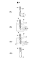
- FIG. 4 is a diagram showing an example of a process of covering the periphery of the element with the first exterior film, where (A) is a diagram of the element provided with the lead terminals, and (B) and (C) are the elements. The figure immersed in the 1st exterior membrane liquid material, (D) is the figure which pulled up the element.
- the element 4 provided with the lead terminals 18, 20 is placed with the lead terminals 18, 20 on the upper side (A), and the liquid material storage part in which the first exterior membrane liquid material 30 is stored.
- the outer membrane liquid material 30 adheres to the periphery of the element 4 (C).
- the outer film liquid material 30 adheres to the periphery. 4 is obtained (D).
- the exterior film liquid material 30 is a viscous liquid, if the element 4 is left in a state of being pulled up, the exterior film liquid material 30 is placed below the element 4 until the exterior film liquid material 30 is dried and cured. It hangs down and the thickness on the lower side becomes thicker. This thickness can be adjusted by time, ambient temperature, heating and the like.
- the exterior film liquid material 30 is applied around the element 4 by heating and curing at 100 [° C.] for 30 minutes.
- the exterior film 8 is formed (Step S7).
- the method of forming the exterior film 8 around the element 4 is not limited to this, and for example, the exterior film liquid material 30 may be applied to the element 4.
- the outer membrane liquid material 30 may be applied by drying and curing.
- FIG. 5 is a diagram showing an example of a process of coating the second exterior film around the first exterior film, and (A) shows a state in which the first exterior film is formed around the element.
- FIGS. 2B and 2C are diagrams in which the first exterior membrane is immersed in the second exterior membrane liquid material, and FIG.
- the lead terminals 18 and 20 are turned upward (A), and the second exterior film is formed.
- the exterior film liquid material 34 adheres to the periphery of the exterior film 8 (C), and when pulled up in this state, the periphery of the exterior film 8
- the varistor 2 is obtained in which the exterior film liquid material 34 adheres to the element 4 and the exterior material 6 composed of the exterior film 8 and the exterior film 10 is formed around the element 4 (D).
- the element 4 on which the exterior film 8 is formed is immersed in the exterior film liquid material 34, pulled up, and then heated and cured at 100 ° C. for 30 minutes for 100 minutes.
- a method of forming the exterior film 10 by applying the exterior film liquid material 34 around the surface 8 may be used.
- membrane 10 can be formed (step S9).
- the exterior film 10 may be any material having explosion resistance such as a material having high rubber elasticity.
- a material having high rubber elasticity such as a material having high rubber elasticity.
- one or more of a silicone resin or a silicone elastomer and aluminum hydroxide, magnesium hydroxide, or calcium hydroxide may be used.
- the exterior film 10 is performed in a reduced pressure atmosphere when the exterior film 8 is immersed in the exterior film liquid material 34, and is released from the reduced pressure atmosphere when it is pulled up from the exterior film liquid material 34 and then cured by heating. You may do it.
- an organic solvent is mixed in the exterior film liquid material 30. Therefore, a void may be formed when the organic solvent volatilizes.
- the exterior film 8 is immersed in the exterior film liquid material 34, pulled up from the exterior film liquid material 34 in a state where the reduced-pressure atmosphere is released, and then cured by heating, so that the air in the voids formed in the exterior film 8 Since the exterior film 10 can be formed in a state in which the film is removed, the exterior film 10 has a substantially uniform thickness, no pinholes or bubbles are involved, flame retardancy is improved, explosion resistance is further improved, and dielectric strength is good. Can be formed.
- the reduced pressure atmosphere when the outer membrane 8 is immersed in the outer membrane liquid material 34 is 5 [kPa] or less. This is because, in a reduced-pressure atmosphere exceeding 5 [kPa], air in the voids of the exterior film 8 may not be sufficiently removed. This is because when air remains in the voids of the exterior film 8, the thickness of the exterior film 10 becomes non-uniform, pinholes and bubbles are involved, and insulation withstand voltage and explosion resistance may not be sufficiently secured. .
- the first exterior film main material does not contain an organic solvent, or when the exterior film 8 is formed so as not to form a void, the exterior film 8 is packaged under a reduced pressure atmosphere. The film liquid material 34 may not be immersed.
- Release of the reduced-pressure atmosphere at the time of pulling up after being immersed in the exterior film liquid material 34 may be any pressure higher than the reduced-pressure atmosphere at the time of immersion of the exterior film 8, and may be, for example, an atmospheric pressure atmosphere. In a pressurized atmosphere.
- the method of forming the exterior film 10 around the exterior film 8 is not limited to the above.
- the exterior film liquid material 34 may be applied to the exterior film 8 or left in place of heat curing.
- the outer membrane liquid material 30 may be applied by drying and curing by blowing air.
- the varistor is exemplified as the electronic component.
- the electronic component formed by covering the element with the exterior material may be an electronic component other than the varistor, and the element is an element such as a transistor or a diode. It may be.
- a first embodiment of the varistor of the present invention will be described.
- a ceramic element is used as the varistor element 12 of the element 4.
- zinc oxide is the main component and magnesium oxide, bismuth oxide, cobalt oxide, etc. are added on both sides of a sintered body having a diameter of 10 mm and a diameter of 8 mm.
- the electrodes 14 and 16 are printed and fired, and the lead terminals 18 and 20 are soldered to the surfaces of the electrodes 14 and 16.
- the varistor element body 12 to which the lead terminals 18 and 20 are soldered is mixed with a liquid first exterior film main material for constituting the exterior film 8 by mixing an organic solvent to obtain an exterior film liquid material 30.
- the exterior film 8 is formed by heating and curing at 100 ° C. for 30 minutes.
- the exterior film liquid material 30 is applied around the element 4 to form the exterior film 8.
- it is preferable to perform heat curing, but for example, it may be cured and fixed by standing drying or air drying.
- the element 4 on which the exterior film 8 is formed is dipped on the exterior film liquid material 34 for constituting the exterior film 10, pulled up, and then heated and cured at 100 ° C. for 30 minutes, and then the exterior film 10. Form.
- Silicone elastomer as the first exterior material is a two-component addition reaction rubber that is cured by mixing a liquid main body and a curing agent and heating to obtain rubber elasticity.
- Table 1 is the data of FIG. 6, and the data in the table indicates the combustion duration time.
- an exterior material in which the ratio of silicone elastomer to aluminum hydroxide is changed between 95: 5 and 5:95 is applied to the element 4. After this coating, the first exterior film is formed by heat curing.
- addition ratio of aluminum hydroxide is the weight ratio of aluminum hydroxide to the weight of the liquid silicone main ingredient combined with the curing agent.
- FIG. 6 confirms the continuous flame time of the exterior film 10 after the application of the rush current, and within the scope of the present invention, there is a flame at the moment when the element 4 reaches a temperature in the vicinity of 1000 [° C.]. However, it absorbs heat instantaneously and the flame disappears. On the other hand, when the amount of aluminum hydroxide is small, the flame continues. It should be noted that there is no scattering of the ceramic contents or the exterior film 8 in the varistor element body 12, and it can be seen that the explosion-proof property is ensured by the exterior film 10.
- FIG. 7 shows a varistor without the exterior film 10 (FIG. 1). Since this varistor 22 is the same as the varistor 2 (FIG. 1) except that the exterior film 10 is not provided, the same reference numerals are given.
- the continuous combustion range of the example when aluminum hydroxide is low, there is similar continuous combustion, there is no scattering, and a scattered state is seen in the non-continuous combustion range. This is more noticeable as the amount of aluminum hydroxide increases. Even within this range, there was no continuous combustion for the samples that did not scatter in a 45/55 pattern or the like with a low scatter rate.
- the exterior film 10 is formed in a normal pressure atmosphere.
- the exterior film 8 is formed into the exterior film liquid material 34 in a reduced pressure atmosphere of 2 [kPa]. It is immersed and pulled up from the outer membrane liquid material 34 under an atmospheric pressure atmosphere to form the outer membrane 10.
- the normal pressure atmosphere is an example of a state in which the condition of the reduced pressure atmosphere is canceled, and is not limited to this.
- the element 4 to which the lead terminals 18 and 20 are soldered is dipped on the exterior film liquid material 30 mixed with an organic solvent, pulled up, and then heated and cured at 100 [° C.] for 30 [minutes] around the element 4.
- the exterior film liquid material 30 is applied to form the exterior film 8.
- the periphery is set to a reduced pressure atmosphere of 2 [kPa], and the element 4 on which the exterior film 8 is formed is dipped in the exterior film liquid material 34.
- the ambient atmosphere is returned to a normal pressure atmosphere, pulled up under this condition, and then heated and cured at 100 [° C.] for 30 [minutes] to form the exterior film 10.
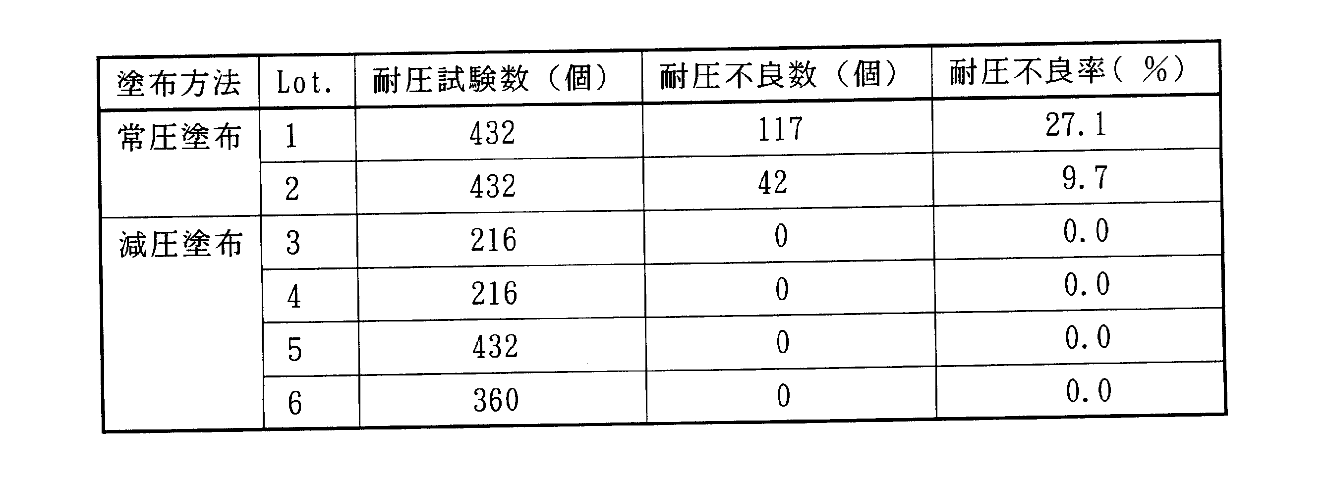
- Table 2 shows the dielectric breakdown voltage of each exterior member 6 using the varistor (reduced pressure application) obtained by the third example and the varistor (normal pressure application) in which the exterior film 10 was formed in an atmospheric pressure atmosphere. It is the result of the test.
- the lead terminals 18 and 20 of the varistor are clamped at the same time, the lead terminals 18 and 20 are used as one pole, a lead ball is brought into contact with the outer surface of the exterior material 6, and this is used as the other. Let it be the pole.
- a potential of 2.5 [kV] is applied between these two electrodes for 60 [seconds] to check whether a short circuit has occurred between the two electrodes.
- the present invention is not limited to this, and it is only necessary to form the exterior film 8 so as not to generate a gap.
- the present invention can be widely used for electronic parts such as varistors and is useful.
Landscapes
- Engineering & Computer Science (AREA)
- Microelectronics & Electronic Packaging (AREA)
- Physics & Mathematics (AREA)
- Electromagnetism (AREA)
- Manufacturing & Machinery (AREA)
- Thermistors And Varistors (AREA)
Abstract
Description
(2) 第一の外装膜主材がほぼ均一に分散されることで、第一の外装膜の不燃性が向上される。
(3) 第一の外装膜の空隙部内の空気を除去した状態で第二の外装膜を形成させれば、厚みがほぼ均一で、ピンホールや気泡巻き込みがなく、難燃性も良好で防爆性がより向上されるとともに、絶縁耐圧が良好な第二の外装膜を形成できる。
の一例であって、素子4と、外装材6として第一の外装膜8及び第二の外装膜10とを備えている。素子4は例えば、電圧非直線性抵抗素子(以下、「バリスタ素子」と称する)であって、バリスタ素体12の表面側に電極14と、その裏面側に電極16とが設置されている。バリスタ素体12の形状は例えば、円盤状であり、電極14、16は表裏面を平行に形成されたバリスタ素体12を挟んで設置されている。
、外装膜液材30が乾燥・硬化するまでの間、外装膜液材30が素子4の下方側に垂下し、該下方側の肉厚が厚くなる。この肉厚は、時間、周囲温度、加熱等によって調整することができる。

場合について説明したが、第2の実施例では、シリコーンエラストマに代えてシリコーン樹脂を用いた場合、水酸化アルミニウムに代えて水酸化マグネシウム又は水酸化カルシウムを用いた場合でも同様の結果が得られた。難燃剤としては、水酸化アルミニウムが主なもので、水酸化マグネシウム及び水酸化カルシウムは同様のメカニズムで難燃性を呈する。
4 素子
6 外装材
8 第一の外装膜
10 第二の外装膜
12 バリスタ素体
30 第一の外装膜液材
34 第二の外装膜液材
Claims (7)
- 外装材で素子を被覆する電子部品の製造方法であって、
有機溶剤を含む第一の外装膜液材を素子に塗着させて第一の外装膜を形成する工程と、
該第一の外装膜に第二の外装膜液材を塗着させて第二の外装膜を形成する工程とを含み、
前記第一の外装膜は、シリコーン樹脂又はシリコーンエラストマと、水酸化アルミニウム、水酸化マグネシウム又は水酸化カルシウムの1種以上とが、重量比45/55~5/95の範囲で含有されていること
を特徴とする電子部品の製造方法。 - 前記第二の外装膜は、
減圧雰囲気下で前記第一の外装膜に前記第二の外装膜液材を塗着した後、前記減圧雰囲気を解除し、加熱硬化されることによって形成されること
を特徴とする請求項1記載の電子部品の製造方法。 - 前記第二の外装膜は、シリコーン樹脂又はシリコーンエラストマと、水酸化アルミニウム、水酸化マグネシウム又は水酸化カルシウムの1種以上とが、重量比100/0~50/50の範囲で含有されていること
を特徴とする請求項1又は2記載の電子部品の製造方法。 - 前記有機溶剤は、前記第一の外装膜主材100重量部に対する重量比が、20~40重量部の範囲であること
を特徴とする請求項1記載の電子部品の製造方法。 - 前記有機溶剤は、イソプロピルアルコールであること
を特徴とする請求項1又は4記載の電子部品の製造方法。 - 前記減圧雰囲気は、5kPa以下であること
を特徴とする請求項2記載の電子部品の製造方法。 - 前記素子が電圧非直線性抵抗素子であること
を特徴とする請求項1乃至6記載の電子部品の製造方法。
Priority Applications (4)
| Application Number | Priority Date | Filing Date | Title |
|---|---|---|---|
| DE112010000695T DE112010000695T5 (de) | 2009-02-16 | 2010-02-15 | Herstellungsverfahren für ein elektronisches Teil |
| CN2010800076250A CN102318016A (zh) | 2009-02-16 | 2010-02-15 | 电子部件的制造方法 |
| KR1020117018792A KR101190900B1 (ko) | 2009-02-16 | 2010-02-15 | 전자 부품의 제조 방법 |
| US13/145,453 US20110274831A1 (en) | 2009-02-16 | 2010-02-15 | Manufacturing method of electronic part |
Applications Claiming Priority (2)
| Application Number | Priority Date | Filing Date | Title |
|---|---|---|---|
| JP2009-033081 | 2009-02-16 | ||
| JP2009033081A JP2010192539A (ja) | 2009-02-16 | 2009-02-16 | 電子部品の製造方法 |
Publications (1)
| Publication Number | Publication Date |
|---|---|
| WO2010092833A1 true WO2010092833A1 (ja) | 2010-08-19 |
Family
ID=42561681
Family Applications (1)
| Application Number | Title | Priority Date | Filing Date |
|---|---|---|---|
| PCT/JP2010/000910 Ceased WO2010092833A1 (ja) | 2009-02-16 | 2010-02-15 | 電子部品の製造方法 |
Country Status (7)
| Country | Link |
|---|---|
| US (1) | US20110274831A1 (ja) |
| JP (1) | JP2010192539A (ja) |
| KR (1) | KR101190900B1 (ja) |
| CN (1) | CN102318016A (ja) |
| DE (1) | DE112010000695T5 (ja) |
| TW (1) | TW201037738A (ja) |
| WO (1) | WO2010092833A1 (ja) |
Cited By (1)
| Publication number | Priority date | Publication date | Assignee | Title |
|---|---|---|---|---|
| US9892830B2 (en) | 2013-11-13 | 2018-02-13 | Nippon Chemi-Con Corporation | Electronic component and production method therefor |
Families Citing this family (10)
| Publication number | Priority date | Publication date | Assignee | Title |
|---|---|---|---|---|
| US10094727B2 (en) | 2013-06-25 | 2018-10-09 | Ngk Spark Plug Co., Ltd. | Knocking sensor |
| JP6349836B2 (ja) * | 2014-03-25 | 2018-07-04 | 住友ベークライト株式会社 | バリスタ用エポキシ樹脂粉体塗料およびバリスタ |
| US20170221612A1 (en) * | 2014-08-08 | 2017-08-03 | Dongguan Littelfuse Electronics, Co., Ltd. | Varistor having multilayer coating and fabrication method |
| CN107833710A (zh) * | 2015-01-05 | 2018-03-23 | 湖南轻创科技有限公司 | 旋转液体可变电阻器、电机启动器 |
| CN105845298A (zh) * | 2016-05-09 | 2016-08-10 | 兴勤(常州)电子有限公司 | 双层树脂包封防水型负温度热敏电阻器 |
| JP7126064B2 (ja) * | 2016-12-28 | 2022-08-26 | パナソニックIpマネジメント株式会社 | 電解コンデンサおよびその製造方法 |
| JP2019009361A (ja) * | 2017-06-27 | 2019-01-17 | 株式会社村田製作所 | セラミック電子部品及びその実装構造 |
| TWM578001U (zh) * | 2018-11-13 | 2019-05-11 | 久尹股份有限公司 | 壓敏電阻結構改良 |
| DE102023104467A1 (de) * | 2023-02-23 | 2024-08-29 | Tdk Electronics Ag | Keramisches Bauelement und Verfahren zur Herstellung eines keramischen Bauelements |
| WO2025249191A1 (ja) * | 2024-05-31 | 2025-12-04 | 株式会社村田製作所 | 電子部品 |
Citations (12)
| Publication number | Priority date | Publication date | Assignee | Title |
|---|---|---|---|---|
| JPH05109506A (ja) * | 1991-10-16 | 1993-04-30 | Fuji Electric Co Ltd | 電圧非直線抵抗体 |
| JPH0897008A (ja) * | 1994-02-21 | 1996-04-12 | Matsushita Electric Ind Co Ltd | バリスタの製造法 |
| JPH08153601A (ja) * | 1994-11-28 | 1996-06-11 | Murata Mfg Co Ltd | 電子部品 |
| JPH11263913A (ja) * | 1998-01-07 | 1999-09-28 | Shin Etsu Chem Co Ltd | 高電圧電気絶縁体用シリコ―ンゴム組成物及びポリマ―碍子 |
| JP2001284103A (ja) * | 2000-03-31 | 2001-10-12 | Okaya Electric Ind Co Ltd | 外装被覆型電子部品 |
| JP2004039999A (ja) * | 2002-07-05 | 2004-02-05 | Nippon Chemicon Corp | バリスタ及びその製造方法 |
| JP2004281934A (ja) * | 2003-03-18 | 2004-10-07 | Nippon Chemicon Corp | 電子部品およびその製造方法 |
| JP2005243746A (ja) * | 2004-02-24 | 2005-09-08 | Nippon Chemicon Corp | バリスタ |
| JP2005277100A (ja) * | 2004-03-24 | 2005-10-06 | Nippon Chemicon Corp | 電子部品 |
| JP2005286253A (ja) * | 2004-03-30 | 2005-10-13 | Nippon Chemicon Corp | 電子部品の製造方法 |
| JP2006286986A (ja) * | 2005-03-31 | 2006-10-19 | Nippon Chemicon Corp | 電子部品およびその製造方法 |
| JP2009088168A (ja) * | 2007-09-28 | 2009-04-23 | Nippon Chemicon Corp | 電子部品 |
Family Cites Families (6)
| Publication number | Priority date | Publication date | Assignee | Title |
|---|---|---|---|---|
| US3621892A (en) * | 1969-09-04 | 1971-11-23 | Thomas J Gillespie | Resin vacuum degassing and dispensing system and method |
| US4247441A (en) * | 1979-02-09 | 1981-01-27 | General Electric Company | Process for preparing a silicone molding composition |
| CA1167364A (en) * | 1980-09-22 | 1984-05-15 | Masayuki Oizumi | Production of bubble-free electrical laminates |
| JPH06215910A (ja) | 1993-01-14 | 1994-08-05 | Tama Electric Co Ltd | 温度ヒューズ付きバリスタ |
| JP4107986B2 (ja) | 2003-03-17 | 2008-06-25 | 京セラミタ株式会社 | 用紙搬送ガイド及びこれを搭載した画像形成装置 |
| JP4421925B2 (ja) * | 2004-03-30 | 2010-02-24 | 三星電子株式会社 | 不揮発性半導体記憶装置 |
-
2009
- 2009-02-16 JP JP2009033081A patent/JP2010192539A/ja active Pending
-
2010
- 2010-02-12 TW TW099104708A patent/TW201037738A/zh unknown
- 2010-02-15 WO PCT/JP2010/000910 patent/WO2010092833A1/ja not_active Ceased
- 2010-02-15 US US13/145,453 patent/US20110274831A1/en not_active Abandoned
- 2010-02-15 DE DE112010000695T patent/DE112010000695T5/de not_active Withdrawn
- 2010-02-15 KR KR1020117018792A patent/KR101190900B1/ko active Active
- 2010-02-15 CN CN2010800076250A patent/CN102318016A/zh active Pending
Patent Citations (12)
| Publication number | Priority date | Publication date | Assignee | Title |
|---|---|---|---|---|
| JPH05109506A (ja) * | 1991-10-16 | 1993-04-30 | Fuji Electric Co Ltd | 電圧非直線抵抗体 |
| JPH0897008A (ja) * | 1994-02-21 | 1996-04-12 | Matsushita Electric Ind Co Ltd | バリスタの製造法 |
| JPH08153601A (ja) * | 1994-11-28 | 1996-06-11 | Murata Mfg Co Ltd | 電子部品 |
| JPH11263913A (ja) * | 1998-01-07 | 1999-09-28 | Shin Etsu Chem Co Ltd | 高電圧電気絶縁体用シリコ―ンゴム組成物及びポリマ―碍子 |
| JP2001284103A (ja) * | 2000-03-31 | 2001-10-12 | Okaya Electric Ind Co Ltd | 外装被覆型電子部品 |
| JP2004039999A (ja) * | 2002-07-05 | 2004-02-05 | Nippon Chemicon Corp | バリスタ及びその製造方法 |
| JP2004281934A (ja) * | 2003-03-18 | 2004-10-07 | Nippon Chemicon Corp | 電子部品およびその製造方法 |
| JP2005243746A (ja) * | 2004-02-24 | 2005-09-08 | Nippon Chemicon Corp | バリスタ |
| JP2005277100A (ja) * | 2004-03-24 | 2005-10-06 | Nippon Chemicon Corp | 電子部品 |
| JP2005286253A (ja) * | 2004-03-30 | 2005-10-13 | Nippon Chemicon Corp | 電子部品の製造方法 |
| JP2006286986A (ja) * | 2005-03-31 | 2006-10-19 | Nippon Chemicon Corp | 電子部品およびその製造方法 |
| JP2009088168A (ja) * | 2007-09-28 | 2009-04-23 | Nippon Chemicon Corp | 電子部品 |
Cited By (1)
| Publication number | Priority date | Publication date | Assignee | Title |
|---|---|---|---|---|
| US9892830B2 (en) | 2013-11-13 | 2018-02-13 | Nippon Chemi-Con Corporation | Electronic component and production method therefor |
Also Published As
| Publication number | Publication date |
|---|---|
| US20110274831A1 (en) | 2011-11-10 |
| KR20110105857A (ko) | 2011-09-27 |
| TW201037738A (en) | 2010-10-16 |
| KR101190900B1 (ko) | 2012-10-12 |
| CN102318016A (zh) | 2012-01-11 |
| DE112010000695T5 (de) | 2012-08-30 |
| JP2010192539A (ja) | 2010-09-02 |
Similar Documents
| Publication | Publication Date | Title |
|---|---|---|
| WO2010092833A1 (ja) | 電子部品の製造方法 | |
| US20080258858A1 (en) | Non-burnable varistor | |
| JP5157349B2 (ja) | 電子部品 | |
| JP6561839B2 (ja) | 電子部品およびその製造方法 | |
| JP4650622B2 (ja) | 電圧非直線性抵抗器 | |
| US7268661B2 (en) | Composite fuse element and methods of making same | |
| JP5047454B2 (ja) | 電子部品 | |
| JP2004095609A (ja) | 外装被覆形バリスタ | |
| JP2004281934A (ja) | 電子部品およびその製造方法 | |
| JP3415094B2 (ja) | 外装被覆型電子部品の製造方法 | |
| JP2005243746A (ja) | バリスタ | |
| JP3171743B2 (ja) | バリスタの製造法 | |
| JP2004039999A (ja) | バリスタ及びその製造方法 | |
| CN101001015B (zh) | 防浪涌保护电路及包含该电路的电源插座 | |
| JP2004247479A (ja) | 電子部品 | |
| JP4513938B2 (ja) | 電子部品 | |
| CN114141460B (zh) | 一种mov防火包封方法 | |
| CN209045265U (zh) | 具阻燃效果的电极电子元件 | |
| TWI703186B (zh) | 塗料組合物、塗層及包含該塗層的壓敏電阻器 | |
| CN111205763B (zh) | 涂料组合物、涂层及包含该涂层的压敏电阻器 | |
| CN120767078A (zh) | 一种用于电涌保护器的压敏电阻器及电涌保护器 | |
| KR102218896B1 (ko) | 정전기 방전 보호용 조성물 및 이 조성물을 이용한 정전기 방전 보호 소자 | |
| JP2002367812A (ja) | 電圧非直線性抵抗器 | |
| JP2009246114A (ja) | 電子部品および電子部品の外装膜形成方法 | |
| JPH06181074A (ja) | 熱接着性可撓性接続部材 |
Legal Events
| Date | Code | Title | Description |
|---|---|---|---|
| WWE | Wipo information: entry into national phase |
Ref document number: 201080007625.0 Country of ref document: CN |
|
| 121 | Ep: the epo has been informed by wipo that ep was designated in this application |
Ref document number: 10741113 Country of ref document: EP Kind code of ref document: A1 |
|
| ENP | Entry into the national phase |
Ref document number: 20117018792 Country of ref document: KR Kind code of ref document: A |
|
| WWE | Wipo information: entry into national phase |
Ref document number: 112010000695 Country of ref document: DE Ref document number: 1120100006954 Country of ref document: DE |
|
| 122 | Ep: pct application non-entry in european phase |
Ref document number: 10741113 Country of ref document: EP Kind code of ref document: A1 |