WO2010087250A1 - セラミック電子部品 - Google Patents
セラミック電子部品 Download PDFInfo
- Publication number
- WO2010087250A1 WO2010087250A1 PCT/JP2010/050571 JP2010050571W WO2010087250A1 WO 2010087250 A1 WO2010087250 A1 WO 2010087250A1 JP 2010050571 W JP2010050571 W JP 2010050571W WO 2010087250 A1 WO2010087250 A1 WO 2010087250A1
- Authority
- WO
- WIPO (PCT)
- Prior art keywords
- ceramic
- metal terminal
- ceramic element
- electrode
- exterior material
- Prior art date
- Legal status (The legal status is an assumption and is not a legal conclusion. Google has not performed a legal analysis and makes no representation as to the accuracy of the status listed.)
- Ceased
Links
Images




Classifications
-
- H—ELECTRICITY
- H01—ELECTRIC ELEMENTS
- H01G—CAPACITORS; CAPACITORS, RECTIFIERS, DETECTORS, SWITCHING DEVICES, LIGHT-SENSITIVE OR TEMPERATURE-SENSITIVE DEVICES OF THE ELECTROLYTIC TYPE
- H01G4/00—Fixed capacitors; Processes of their manufacture
- H01G4/002—Details
- H01G4/228—Terminals
-
- H—ELECTRICITY
- H01—ELECTRIC ELEMENTS
- H01G—CAPACITORS; CAPACITORS, RECTIFIERS, DETECTORS, SWITCHING DEVICES, LIGHT-SENSITIVE OR TEMPERATURE-SENSITIVE DEVICES OF THE ELECTROLYTIC TYPE
- H01G4/00—Fixed capacitors; Processes of their manufacture
- H01G4/002—Details
- H01G4/224—Housing; Encapsulation
-
- H—ELECTRICITY
- H01—ELECTRIC ELEMENTS
- H01C—RESISTORS
- H01C1/00—Details
- H01C1/01—Mounting; Supporting
- H01C1/014—Mounting; Supporting the resistor being suspended between and being supported by two supporting sections
-
- H—ELECTRICITY
- H01—ELECTRIC ELEMENTS
- H01C—RESISTORS
- H01C1/00—Details
- H01C1/14—Terminals or tapping points specially adapted for resistors; Arrangements of terminals or tapping points on resistors
- H01C1/148—Terminals or tapping points specially adapted for resistors; Arrangements of terminals or tapping points on resistors the terminals embracing or surrounding the resistive element
-
- H—ELECTRICITY
- H01—ELECTRIC ELEMENTS
- H01C—RESISTORS
- H01C7/00—Non-adjustable resistors formed as one or more layers or coatings; Non-adjustable resistors made from powdered conducting material or powdered semi-conducting material with or without insulating material
- H01C7/10—Non-adjustable resistors formed as one or more layers or coatings; Non-adjustable resistors made from powdered conducting material or powdered semi-conducting material with or without insulating material voltage responsive, i.e. varistors
-
- H—ELECTRICITY
- H01—ELECTRIC ELEMENTS
- H01G—CAPACITORS; CAPACITORS, RECTIFIERS, DETECTORS, SWITCHING DEVICES, LIGHT-SENSITIVE OR TEMPERATURE-SENSITIVE DEVICES OF THE ELECTROLYTIC TYPE
- H01G2/00—Details of capacitors not covered by a single one of groups H01G4/00-H01G11/00
- H01G2/02—Mountings
- H01G2/06—Mountings specially adapted for mounting on a printed-circuit support
Definitions
- This invention relates to ceramic electronic components such as ceramic capacitors and ceramic varistors.
- the medium- and high-voltage ceramic capacitors with a rating of 3 kV or more are mainly in-line mounting type with lead wires.
- the demand for surface mount types is increasing.
- This surface-mount type ceramic capacitor has ceramic elements with electrodes formed on both opposing main surfaces, two metal terminals connected to each electrode, and insulation that embeds part of the ceramic elements and metal terminals. And an exterior packaging material. The metal terminal is pulled out from the side surface of the insulating exterior material, and is bent from the side surface to the bottom end.
- the metal terminal is firmly fixed by the insulating exterior material, and mechanical stress when the mounting substrate is bent is directly applied to the ceramic element, and the ceramic element is cracked. There was a problem that it occurred. Further, in the conventional surface mount type ceramic capacitor, there is a possibility that the creeping discharge when the high voltage is applied cannot be sufficiently prevented because the creeping distance of the insulating exterior material between the two metal terminals is short.
- a main object of the present invention is to provide a ceramic electronic component in which mechanical stress when a mounting board is bent is not directly applied to a ceramic element and creeping discharge can be prevented.
- the insulating exterior material is molded by injection molding or transfer molding.
- the ceramic is prevented to prevent creeping discharge.
- An electrode cannot be formed on the entire main surface of the element, and it is necessary to form the electrode by retreating from the outer peripheral edge of the main surface. For this reason, there is a restriction that the ceramic element cannot be reduced in size.
- the insulating exterior material is formed by transfer molding a thermosetting resin, but the yield of the insulating exterior material is poor and the productivity is not good.
- the present invention includes a ceramic substrate having a first main surface and a second main surface opposite to each other on an outer peripheral surface, a first electrode provided on the first main surface, and a second electrode provided on the second main surface, , A first metal terminal joined to the first electrode, a second metal terminal joined to the second electrode, a ceramic element, a part of the first metal terminal and one of the second metal terminals A ceramic electronic component comprising an insulating exterior material covering a portion, The first metal terminal extends parallel to the first main surface and is joined to the first electrode, and extends parallel to the first joint and is mounted on the mounting substrate.
- the second metal terminal extends parallel to the second main surface and joined to the second electrode, and extends parallel to the second joint and is mounted on the mounting substrate.
- the insulating exterior material is provided so as to cover the ceramic element, the first joint portion, the first relay portion, and the second joint portion, and so that the first mounting portion and the second mounting portion are exposed, In a portion where the outer peripheral surface of the ceramic substrate and the first relay portion of the first metal terminal face each other, an insulating exterior material that covers the outer peripheral surface of the ceramic substrate and an insulating property that covers the first relay portion of the first metal terminal
- a ceramic electronic component characterized in that a space is formed between the outer packaging material and the outer packaging material.
- the first electrode and the second electrode may be provided on the entire surfaces of the first main surface and the second main surface, respectively.
- a space is formed between the insulating exterior material covering the outer peripheral surface of the ceramic element and the insulating exterior material covering the first relay portion of the first metal terminal. Therefore, the boundary portion between the first joint portion and the first relay portion of the first metal terminal has a spring property due to this space, and mechanical stress when the mounting board is bent is applied to the boundary portion. Mechanical stress is not directly applied to the ceramic element. Furthermore, this space increases the creeping distance of the insulating exterior material between the first mounting part of the first metal terminal and the second mounting part of the second metal terminal, and creeping discharge when a high voltage is applied. Less likely to occur. Furthermore, the amount of the insulating exterior material used is reduced, and it is not always necessary to use a mold when forming the insulating exterior material.
- the width dimension of the first joint portion of the first metal terminal is larger than the width dimension of the ceramic element, and the edge portion of the ceramic element recedes from the edge portion of the first joint portion in a plan view.
- a fillet made of a bonding material for bonding the first electrode of the ceramic element and the first metal terminal is formed between the edge of the ceramic element and the first bonding portion, and the first A bonding material or a bonding material and an insulating exterior material are filled between the electrode and the first bonding portion.
- the bonding material is filled between the edge of the ceramic element and the first metal terminal, and there is no space between the first electrode and the first bonding portion, and high frequency is generated in the ceramic electronic component. Creeping discharge when applied is prevented.
- the present invention is characterized in that the minimum distance between the second electrode and the second metal terminal of the ceramic element and the first metal terminal is equal to or greater than the thickness dimension of the ceramic substrate.
- each of the first joint portion and the second joint portion has a convex portion protruding toward the ceramic element side.
- a gap is formed between the first and second joint portions and the first and second main surfaces of the ceramic element, and the bending stress of the first and second metal terminals is not directly applied to the edge portion of the ceramic element.
- the insulating exterior material is characterized by comprising an epoxy-based powder resin.
- a flat portion having a diameter of about 2.5 mm or more is provided on the upper surface of the insulating exterior material, and a portion protruding upward is provided in a range having a diameter of about 4 mm or more in the same center as the flat portion. It is characterized by not. Thereby, the ceramic electronic component which can be attracted
- the space is formed between the insulating exterior material that covers the outer peripheral surface of the ceramic element and the insulating exterior material that covers the first relay portion of the first metal terminal.
- the boundary portion between the first joint portion of the first metal terminal and the first relay portion has a spring property, and mechanical stress when the mounting substrate is bent is applied to the boundary portion, and mechanically. Stress is not directly applied to the ceramic element.
- this space increases the creeping distance of the insulating exterior material between the first mounting portion of the first metal terminal and the second mounting portion of the second metal terminal, and causes creeping discharge when a high voltage is applied. Can be suppressed.
- the amount of the insulating exterior material used can be reduced, and when the insulating exterior material is formed, it is not always necessary to use a mold, so that the production efficiency is good. As a result, it is possible to obtain a ceramic electronic component in which mechanical stress when the mounting substrate is bent is not directly applied to the ceramic element, and creeping discharge can be prevented.
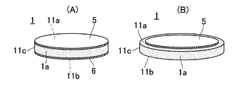
- (A) is a plan view of the ceramic electronic component of the first embodiment, and (B) is a sectional view taken along the line II of (A). It is a perspective view which shows a ceramic element.
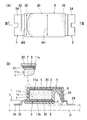
- (A) is a plan view of the ceramic electronic component of the second embodiment, and (B) is a sectional view taken along the line III-III of (A).
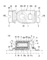
- (A) is a top view of the ceramic electronic component of 3rd Embodiment, (B) is IV-IV sectional drawing of (A).
- (A) is a plan view of the ceramic electronic component of the fourth embodiment, (B) is a side view thereof, and (C) is a VV sectional view of (A).
- (A) is a top view of the ceramic electronic component of 5th Embodiment
- (B) is VI-VI sectional drawing of (A).
- (A) is a top view of the ceramic electronic component of 6th Embodiment
- (B) is VII-VII sectional drawing of (A).
- FIG. 1A is a plan view of the surface mount type ceramic capacitor of the first embodiment
- FIG. 1B is a cross-sectional view taken along the line II of FIG. 1A.
- the ceramic capacitor is formed by covering a disk-shaped ceramic element 1 made of BaTiO 3 or the like, metal terminals 2 and 3 bonded to the front and back of the ceramic element 1, and part of the ceramic element 1 and the metal terminals 2 and 3.
- the insulating exterior material 4 is provided.
- the ceramic element 1 has a ceramic substrate having a front surface 11a and a back surface 11b facing each other, and an outer peripheral surface 11c.
- electrodes 5 and 6 are formed on the entire surface 11a and back surface 11b of the ceramic substrate 1a.
- the electrodes 5 and 6 are made of Ni, Cu, Ag, Cr, or an alloy mainly containing any one of these, and are formed by an electroless plating method, a vapor deposition method, or a printing method.
- the electrodes 5 and 6 may be formed so as to recede from the outer peripheral edge of the ceramic substrate 1a without being formed on the entire surface 11a and back surface 11b.
- Metal terminals 2 and 3 are formed by bending. That is, the metal terminal 2 extends in parallel to the surface 11a and is bonded to the electrode 5, and the mounting portion that extends in parallel to the bonding portion 20 and is mounted on the mounting substrate P. 24 and a relay part 22 that connects the joint part 20 and the mounting part 24.
- the joint portion 20 protrudes relatively long from the edge of the ceramic element 1, and the relay portion 22 extends in a substantially vertical direction.
- the metal terminal 3 extends in parallel to the back surface 11b and is bonded to the electrode 6, and the mounting that extends in parallel to the bonding portion 30 and is mounted on the mounting substrate P. Part 34, and a relay part 32 that connects the joint part 30 and the mounting part 34.
- the relay part 32 extends in a substantially vertical direction.
- the mounting portions 24 and 34 of the metal terminals 2 and 3 are led out to the left and right opposite sides with the ceramic element 1 therebetween.
- the material of the metal terminals 2 and 3 is preferably a material having a linear expansion coefficient close to that of the ceramic element 1 such as SUS430.
- the surface of the metal terminals 2 and 3 is Sn plated, and a base plating such as Ni may be applied as necessary.
- a conductive adhesive mainly composed of Ag powder or Cu powder coated with Ag, or lead such as LF high-temperature solder is contained. Bonding material that is not used is used.
- the insulating exterior material 4 is provided so as to cover the ceramic element 1, the joint portion 20 and the relay portion 22 of the metal terminal 2, and the joint portion 30 of the metal terminal 3.
- the mounting portions 24 and 34 of the metal terminals 2 and 3 are exposed from the insulating exterior material 4.
- an epoxy powder resin, a silicone resin, or the like is used, and is formed by a dipping method or the like.
- an epoxy powder resin is used as the insulating exterior material 4 it has good adhesion to the ceramic element 1 and the metal terminals 2 and 3 and can secure high sealing performance, so that creeping discharge hardly occurs.
- the electrodes 5 and 6 can be formed on the entire surface 11a and back surface 11b of the ceramic substrate 1a, and a small ceramic capacitor can be obtained while maintaining high withstand voltage characteristics.
- the adhesion between the insulating exterior material 4 and the ceramic element 1 is improved, the yield of the insulating exterior material 4 is good, and high productivity is achieved. Obtainable.
- covers the outer peripheral surface 11c of the ceramic substrate 1a, and the relay part 22 of the metal terminal 2 are coat
- the surface mount type ceramic capacitor having the above configuration is formed between the insulating exterior material 4 covering the outer peripheral surface 11 c of the ceramic element 1 and the insulating exterior material 4 covering the relay portion 22 of the metal terminal 2.
- the creeping distance of the insulating exterior material 4 between the mounting portion 24 of the metal terminal 2 and the mounting portion 34 of the metal terminal 3 is increased by the space S, and creeping discharge when high voltage is applied is suppressed. Can do.
- the boundary portion between the joint portion 20 and the relay portion 22 of the metal terminal 2 has a spring property, and mechanical stress when the mounting substrate P is bent is applied to the boundary portion, Mechanical stress is not directly applied to the ceramic element 1.
- FIG. 3A is a plan view of the surface-mount type ceramic capacitor of the second embodiment
- FIG. 3B is a cross-sectional view taken along the line III-III of FIG.
- the ceramic capacitor includes a disk-shaped ceramic element 1, metal terminals 2 and 3 bonded to the front and back of the ceramic element 1, and an insulating exterior material covering a part of the ceramic element 1 and the metal terminals 2 and 3. 4 is provided.
- the ceramic element 1 is the same as that described in the first embodiment, and a detailed description thereof is omitted.
- the metal terminal 2 extends in parallel to the surface 11a and is bonded to the electrode 5, and the mounting portion 24 that extends in parallel to the bonding portion 20 and is mounted on the mounting substrate P.
- the relay unit 22 connects the joint unit 20 and the mounting unit 24.
- the metal terminal 3 extends in parallel to the back surface 11b and is bonded to the electrode 6, and the mounting that extends in parallel to the bonding portion 30 and is mounted on the mounting substrate P.
- Part 34, and a relay part 32 that connects the joint part 30 and the mounting part 34.
- the width dimensions W1 and W2 of the joint portions 20 and 30 of the metal terminals 2 and 3 are designed to be larger than the diameter D of the ceramic element 1, and the edge portion of the ceramic element 1 is the edge portion of the joint portions 20 and 30 in a plan view. It is more backward.
- the metal terminals 2 and 3 and the electrodes 5 and 6 are joined together by a joining material 7.
- a fillet 61 made of the bonding material 7 is formed between the edge of the ceramic element 1 and the bonding portions 20 and 30 of the metal terminals 2 and 3.
- the minimum distance d between the electrode 6 and the metal terminal 3 provided on the back surface 11b of the ceramic substrate 1a and the metal terminal 2 is designed to be equal to or greater than the thickness dimension T of the ceramic substrate 1a.
- the insulating exterior material 4 is provided so as to cover the ceramic element 1, the joint portion 20 and the relay portion 22 of the metal terminal 2, and the joint portion 30 of the metal terminal 3.
- the mounting portions 24 and 34 of the metal terminals 2 and 3 are exposed from the insulating exterior material 4.
- covers the outer peripheral surface 11c of the ceramic substrate 1a, and the relay part 22 of the metal terminal 2 are coat
- the surface mount type ceramic capacitor having the above configuration is formed between the insulating exterior material 4 covering the outer peripheral surface 11 c of the ceramic element 1 and the insulating exterior material 4 covering the relay portion 22 of the metal terminal 2.
- the creeping distance of the insulating exterior material 4 between the mounting portion 24 of the metal terminal 2 and the mounting portion 34 of the metal terminal 3 is increased by the space S, and creeping discharge when high voltage is applied is suppressed. Can do.
- the boundary portion between the joint portion 20 and the relay portion 22 of the metal terminal 2 has a spring property, and mechanical stress when the mounting substrate P is bent is applied to the boundary portion, Mechanical stress is not directly applied to the ceramic element 1.
- the widths W1 and W2 of the joint portions 20 and 30 of the metal terminals 2 and 3 are designed to be larger than the diameter D of the ceramic element 1, and the edge of the ceramic element 1 of the joint portions 20 and 30 is seen through in plan view. Since it recedes from the edge portion, the electric field concentration at the edge portion of the ceramic element 1 can be relaxed, and a small and high withstand voltage capacitor can be manufactured.
- the widths W1 and W2 of the joints 20 and 30 of the metal terminals 2 and 3 are designed to be larger than the diameter D of the ceramic element 1, but at least the joints of the upper metal terminal 2 If the width dimension W1 of 20 is designed to be larger than the diameter D of the ceramic element 1, the effect of relaxing the electric field concentration at the edge of the ceramic element 1 can be obtained.
- fillets 61 made of the bonding material 7 are formed between the edge of the ceramic element 1 and the joints 20 and 30 of the metal terminals 2 and 3, respectively, and between the electrode 5 and the joint 20 and the electrode 6. And the joining portion 30 are filled with the joining material 7, respectively.
- the bonding material 7 is filled between the edge of the ceramic element 1 and the bonding portions 20, 30, and between the electrode 5 and the bonding portion 20 and between the electrode 6 and the bonding portion 30. Therefore, creeping discharge can be prevented when a high frequency is applied to the ceramic electronic component.
- the minimum distance d between the electrode 6 and the metal terminal 3 provided on the back surface 11b of the ceramic substrate 1a and the metal terminal 2 is designed to be equal to or greater than the thickness dimension T of the ceramic substrate 1a, the insulating property is improved.
- a ceramic capacitor having the design withstand voltage of the ceramic element 1 itself can be obtained without being affected by the thickness of the exterior material 4.
- the electrodes 5 and 6 are formed on the entire surface 11a and back surface 11b as shown in FIG.
- the electrode 5 is formed by retreating from the outer peripheral edge portion of the ceramic substrate 1a without being formed on the entire surface 11a and the back surface 11b. , 6 has to be provided around the gap.
- the second embodiment as shown in FIG.
- a fillet 61 is formed so that no space exists between the electrodes 5 and 6 and the metal terminals 2 and 3. Since creeping discharge is prevented, the electrodes 5 and 6 can be formed on the entire surface 11a and back surface 11b of the ceramic substrate 1a. Therefore, the portion of the ceramic substrate 1a around the electrodes 5 and 6, which has been necessary in the past, becomes unnecessary, and the ceramic element 1 can be downsized.
- FIG. 4A is a plan view of the surface mount type ceramic capacitor of the third embodiment
- FIG. 4B is a cross-sectional view taken along the line IV-IV in FIG. 4A
- the ceramic capacitor of the third embodiment is a modification of the ceramic capacitor of the second embodiment, and includes a disk-shaped ceramic element 1 and metal terminals 2 and 3 bonded to the front and back of the ceramic element 1. And an insulating exterior material 4 covering a part of the ceramic element 1 and the metal terminals 2 and 3.
- FIGS. 4A and 4B the same components and parts as those in the second embodiment are denoted by the same reference numerals, and detailed description thereof is omitted.
- the width dimensions W1 and W2 of the joint portions 20 and 30 of the metal terminals 2 and 3 are designed to be larger than the diameter D of the ceramic element 1, and the edge portion of the ceramic element 1 is the edge portion of the joint portions 20 and 30 in a plan view. It is more backward.
- the joint portions 20 and 30 of the metal terminals 2 and 3 may be designed so that the edge portion of the ceramic element 1 recedes from the edge portion of the joint portions 20 and 30.
- a part of the protruding joints 20 and 30 may be cut out to narrow the width dimension W1 ′.
- the joint portion 20 of the metal terminal 2 is designed so that the edge portion of the ceramic element 1 recedes from the edge portion of the joint portion 20, a hole is provided. You may provide 20a, 20b as needed.
- FIG. 5A is a plan view of the surface mount type ceramic capacitor of the fourth embodiment
- FIG. 5B is a side view thereof
- FIG. 5C is a V- It is V sectional drawing.
- the ceramic capacitor includes a disk-shaped ceramic element 1, metal terminals 2 and 3 bonded to the front and back of the ceramic element 1, and an insulating exterior material covering a part of the ceramic element 1 and the metal terminals 2 and 3. 4 is provided.
- the ceramic element 1 is the same as that described in the first embodiment, and a detailed description thereof is omitted.
- the metal terminal 2 extends in parallel to the surface 11a and is bonded to the electrode 5, and the mounting portion 24 that extends in parallel to the bonding portion 20 and is mounted on the mounting substrate P.
- the relay unit 22 connects the joint unit 20 and the mounting unit 24.
- the metal terminal 3 extends in parallel to the back surface 11b and is bonded to the electrode 6, and the mounting that extends in parallel to the bonding portion 30 and is mounted on the mounting substrate P.
- Part 34, and a relay part 32 that connects the joint part 30 and the mounting part 34.
- the width dimensions W1 and W2 of the joint portions 20 and 30 of the metal terminals 2 and 3 are designed to be larger than the diameter D of the ceramic element 1, and the edge portion of the ceramic element 1 is the edge portion of the joint portions 20 and 30 in a plan view. It is more backward.
- the joint portion 20 is formed with a circular hole 20a and a rectangular hole 20b extending to the relay portion 22, and a plurality of substantially conical convex portions 26 projecting toward the ceramic element 1 are provided around the circular hole 20a. Is provided.
- a circular hole 30a is formed in the joint portion 30, and a plurality of substantially conical convex portions 26 protruding toward the ceramic element 1 are provided around the circular hole 30a.
- the circular holes 20 a and 30 a are for supplying the bonding material 7 in the vicinity of the convex portion 26.
- a space between the electrode 5 and the bonding portion 20 and a space between the electrode 6 and the bonding portion 30 are filled with the bonding material 7 and the insulating exterior material 4.
- the rectangular hole 20b is for facilitating the supply of the insulating exterior material 4 to the outer peripheral surface 11c of the ceramic substrate 1a. If the thickness of the metal terminals 2 and 3 is 0.2 mm or less and the height of the convex portion 26 is about 0.2 mm or less, the step due to the circular holes 20a and 30a is filled at the stage of forming the insulating exterior material 4. The upper surface of the insulating exterior material 4 becomes flat and does not adversely affect the adsorption by the automatic mounting machine.
- the insulating exterior material 4 is provided so as to cover the ceramic element 1, the joint portion 20 and the relay portion 22 of the metal terminal 2, and the joint portion 30 of the metal terminal 3.
- the mounting portions 24 and 34 of the metal terminals 2 and 3 are exposed from the insulating exterior material 4.
- covers the outer peripheral surface 11c of the ceramic substrate 1a, and the relay part 22 of the metal terminal 2 are coat
- the surface-mounting type ceramic capacitor having the above configuration has the same effect as the ceramic capacitor of the second embodiment, and each of the joint portions 20 and 30 has a protruding portion 26 protruding to the ceramic element 1 side. Therefore, gaps are formed between the joint portions 20, 30 and the front and back surfaces 11 a, 11 b of the ceramic element 1, and the bending stress of the metal terminals 2, 3 is not directly applied to the edge portion E of the ceramic element 1. Thereby, the tolerance with respect to the bending of the mounting board
- the convex portion 26 also has a function of attracting the bonding material 7 by capillary action, and has an effect of suppressing generation of voids due to contraction when the bonding material 7 is solidified.
- the height of the convex portion 26 is desirably set to about 0.1 to 0.3 mm.
- FIG. 6A is a plan view of a surface mount type ceramic capacitor according to the fifth embodiment
- FIG. 6B is a cross-sectional view taken along the line VI-VI in FIG.
- the ceramic capacitor of the fifth embodiment is a modification of the ceramic capacitor of the fourth embodiment, and includes a disk-shaped ceramic element 1 and metal terminals 2 and 3 joined to the front and back of the ceramic element 1. And an insulating exterior material 4 covering a part of the ceramic element 1 and the metal terminals 2 and 3.
- 6A and 6B the same parts and the same parts as those of the fourth embodiment are denoted by the same reference numerals, and detailed description thereof is omitted.
- a circular hole 20a and a rectangular hole 20b are formed in the joint portion 20 of the metal terminal 2, and an annular convex portion 26 having a substantially conical cross-sectional shape protruding toward the ceramic element 1 is formed around the circular hole 20a. Is provided.
- a circular hole 30 a is formed in the joint portion 30 of the metal terminal 3, and an annular convex portion 26 having a substantially conical cross section protruding toward the ceramic element 1 is provided around the circular hole 30 a. Yes.
- FIG. 7A is a plan view of a surface mount type ceramic capacitor according to the sixth embodiment
- FIG. 7B is a cross-sectional view taken along the line VII-VII in FIG. 7A.
- the ceramic capacitor includes a disk-shaped ceramic element 1, metal terminals 2 and 3 bonded to the front and back of the ceramic element 1, and an insulating exterior material covering a part of the ceramic element 1 and the metal terminals 2 and 3. 4 is provided.
- the ceramic element 1 is the same as that described in the first embodiment, and a detailed description thereof is omitted.
- the metal terminal 2 extends substantially parallel to the surface 11 a and is bonded to the electrode 5, and the mounting portion 24 that extends parallel to the bonding portion 20 and is mounted on the mounting substrate P. And a relay portion 22 that connects the joint portion 20 and the mounting portion 24.
- a step 21 is formed at the joint 20.
- the metal terminal 3 extends in parallel to the back surface 11b and is bonded to the electrode 6, and the mounting that extends in parallel to the bonding portion 30 and is mounted on the mounting substrate P.
- Part 34, and a relay part 32 that connects the joint part 30 and the mounting part 34.
- the relay part 32 is bent into a substantially inverted U shape.
- each of the joint portions 20 and 30 is provided with a plurality of substantially conical convex portions 26 protruding toward the ceramic element 1 side.
- the insulating exterior material 4 is provided so as to cover the ceramic element 1, the joint portion 20 and the relay portion 22 of the metal terminal 2, and the joint portion 30 and the relay portion 32 of the metal terminal 3.
- the mounting portions 24 and 34 of the metal terminals 2 and 3 are exposed from the insulating exterior material 4.
- a flat portion having a diameter of approximately 2.5 mm or more is provided on the upper surface of the insulating exterior material 4, and a portion projecting upward within a range having a diameter of approximately 4 mm or more in the same center as the flat portion is not provided. Thereby, a ceramic capacitor that can be attracted by an automatic mounting machine is obtained.
- a flat portion with a diameter of approximately 2.5 mm or more on the upper surface of the insulating exterior material 4 a flat portion with a diameter of approximately 3.5 mm or more may be provided on the metal terminal 2.
- the metal terminal 2 may have a convex portion 26 or a hole as long as it can be smoothed by the insulating exterior material 4.
- covers the outer peripheral surface 11c of the ceramic substrate 1a, and the relay part 22 of the metal terminal 2 are coat
- a space S ⁇ b> 1 is formed between the insulating exterior material 4 to be formed.
- the insulating exterior material 4 that covers the outer peripheral surface 11c of the ceramic substrate 1a and the relay portion 32 of the metal terminal 3 are provided.
- a space S2 is formed between the insulating exterior material 4 to be covered.
- the surface mount type ceramic capacitor having the above configuration is formed between the insulating exterior material 4 covering the outer peripheral surface 11 c of the ceramic element 1 and the insulating exterior material 4 covering the relay portion 22 of the metal terminal 2.
- the mounting portion 24 of the metal terminal 2 and the mounting portion 34 of the metal terminal 3 are formed by the space S1 formed between the space S1 formed and the insulating exterior material 4 covering the relay portion 32 of the metal terminal 3.
- the creeping distance of the insulating exterior material 4 between the two is increased, and creeping discharge when a high voltage is applied can be suppressed.
- the spaces S1 and S2 have spring properties at the boundary portion between the joint portion 20 and the relay portion 22 of the metal terminal 2 and the boundary portion between the joint portion 30 and the relay portion 32 of the metal terminal 3.
- the ceramic electronic component may be a varistor or the like in addition to the capacitor.
Landscapes
- Engineering & Computer Science (AREA)
- Power Engineering (AREA)
- Microelectronics & Electronic Packaging (AREA)
- Manufacturing & Machinery (AREA)
- Physics & Mathematics (AREA)
- Electromagnetism (AREA)
- Ceramic Capacitors (AREA)
- Thermistors And Varistors (AREA)
Abstract
Description
第1金属端子は、第1主面に対して平行に延在して第1電極に接合された第1接合部と、第1接合部に対して平行に延在して実装基板に実装される第1実装部と、第1接合部と第1実装部とを繋ぐ第1中継部と、を有し、
第2金属端子は、第2主面に対して平行に延在して第2電極に接合された第2接合部と、第2接合部に対して平行に延在して実装基板に実装される第2実装部と、第2接合部と第2実装部とを繋ぐ第2中継部と、を有し、
絶縁性外装材は、セラミック素子、第1接合部、第1中継部および第2接合部を被覆するように、かつ、第1実装部および第2実装部が露出するように設けられ、
セラミック基板の外周面と第1金属端子の第1中継部とが対向する部分において、セラミック基板の外周面を被覆する絶縁性外装材と、第1金属端子の第1中継部を被覆する絶縁性外装材との間に、空間が形成されていること、を特徴とする、セラミック電子部品である。第1電極および前記第2電極はそれぞれ、第1主面および第2主面の全面に設けられていてもよい。
図1(A)は第1の実施形態の表面実装タイプのセラミックコンデンサの平面図であり、図1(B)は図1(A)のI-I断面図である。セラミックコンデンサは、BaTiO3などからなる円板状のセラミック素子1と、セラミック素子1の表裏に接合された金属端子2,3と、セラミック素子1および金属端子2,3の一部を被覆している絶縁性外装材4とを備えている。
図3(A)は第2の実施形態の表面実装タイプのセラミックコンデンサの平面図であり、図3(B)は図3(A)のIII-III断面図である。セラミックコンデンサは、円板状のセラミック素子1と、セラミック素子1の表裏に接合された金属端子2,3と、セラミック素子1および金属端子2,3の一部を被覆している絶縁性外装材4とを備えている。なお、セラミック素子1は、前記第1の実施形態で説明したものと同様のものであり、その詳細な説明は省略する。
図4(A)は第3の実施形態の表面実装タイプのセラミックコンデンサの平面図であり、図4(B)は図4(A)のIV-IV断面図である。第3の実施形態のセラミックコンデンサは、前記第2の実施形態のセラミックコンデンサを変形したものであり、円板状のセラミック素子1と、セラミック素子1の表裏に接合された金属端子2,3と、セラミック素子1および金属端子2,3の一部を被覆している絶縁性外装材4とを備えている。なお、図4(A),(B)において前記第2の実施形態と同一部品および同一部分には同じ符号を付し、その詳細な説明は省略する。
図5(A)は第4の実施形態の表面実装タイプのセラミックコンデンサの平面図であり、図5(B)はその側面図であり、図5(C)は図5(A)のV-V断面図である。セラミックコンデンサは、円板状のセラミック素子1と、セラミック素子1の表裏に接合された金属端子2,3と、セラミック素子1および金属端子2,3の一部を被覆している絶縁性外装材4とを備えている。なお、セラミック素子1は、前記第1の実施形態で説明したものと同様のものであり、その詳細な説明は省略する。
図6(A)は第5の実施形態の表面実装タイプのセラミックコンデンサの平面図であり、図6(B)は図6(A)のVI-VI断面図である。第5の実施形態のセラミックコンデンサは、前記第4の実施形態のセラミックコンデンサを変形したものであり、円板状のセラミック素子1と、セラミック素子1の表裏に接合された金属端子2,3と、セラミック素子1および金属端子2,3の一部を被覆している絶縁性外装材4とを備えている。なお、図6(A),(B)において前記第4の実施形態と同一部品および同一部分には同じ符号を付し、その詳細な説明は省略する。
図7(A)は第6の実施形態の表面実装タイプのセラミックコンデンサの平面図であり、図7(B)は図7(A)のVII-VII断面図である。セラミックコンデンサは、円板状のセラミック素子1と、セラミック素子1の表裏に接合された金属端子2,3と、セラミック素子1および金属端子2,3の一部を被覆している絶縁性外装材4とを備えている。なお、セラミック素子1は、前記第1の実施形態で説明したものと同様のものであり、その詳細な説明は省略する。
なお、この発明は、前記実施形態に限定されるものではなく、その要旨の範囲内で種々に変形される。セラミック電子部品としては、コンデンサの他にバリスタなどであってもよい。
1a セラミック基板
2,3 金属端子
4 絶縁性外装材
5,6 電極
7 接合材
11a 表面(第1主面)
11b 裏面(第2主面)
11c 外周面
20,30 接合部
22,32 中継部
24,34 実装部
26 凸部
61 フィレット
S,S1,S2 空間
Claims (8)
- 外周面と互いに対向する第1主面および第2主面とをもつセラミック基板と、前記第1主面に設けた第1電極および前記第2主面に設けた第2電極と、を有するセラミック素子と、
前記第1電極に接合された第1金属端子と、
前記第2電極に接合された第2金属端子と、
前記セラミック素子、前記第1金属端子の一部および前記第2金属端子の一部を被覆した絶縁性外装材と、
を備えたセラミック電子部品であって、
前記第1金属端子は、前記第1主面に対して平行に延在して前記第1電極に接合された第1接合部と、前記第1接合部に対して平行に延在して実装基板に実装される第1実装部と、前記第1接合部と前記第1実装部とを繋ぐ第1中継部と、を有し、
前記第2金属端子は、前記第2主面に対して平行に延在して前記第2電極に接合された第2接合部と、前記第2接合部に対して平行に延在して前記実装基板に実装される第2実装部と、前記第2接合部と前記第2実装部とを繋ぐ第2中継部と、を有し、
前記絶縁性外装材は、前記セラミック素子、前記第1接合部、前記第1中継部および前記第2接合部を被覆するように、かつ、前記第1実装部および前記第2実装部が露出するように設けられ、
前記セラミック基板の外周面と前記第1金属端子の第1中継部とが対向する部分において、前記セラミック基板の外周面を被覆する前記絶縁性外装材と、前記第1金属端子の第1中継部を被覆する前記絶縁性外装材との間に、空間が形成されていること、
を特徴とする、セラミック電子部品。 - 前記第1電極および前記第2電極がそれぞれ、前記第1主面および前記第2主面の全面に設けられていることを特徴とする、請求項1に記載のセラミック電子部品。
- 前記第1金属端子の第1接合部の幅寸法が前記セラミック素子の幅寸法より大きく、平面透視で前記セラミック素子の縁部が前記第1接合部の縁部より後退していることを特徴とする、請求項1または請求項2に記載のセラミック電子部品。
- 前記セラミック素子の縁部と前記第1接合部との間に、前記セラミック素子の第1電極と前記第1金属端子とを接合するための接合材によるフィレットが形成され、かつ、前記第1電極と前記第1接合部との間に前記接合材もしくは前記接合材および前記絶縁性外装材が充填されていることを特徴とする、請求項3に記載のセラミック電子部品。
- 前記セラミック素子の第2電極および前記第2金属端子と、前記第1金属端子との最小間隔が、前記セラミック基板の厚み寸法以上であることを特徴とする、請求項1~請求項4のいずれかに記載のセラミック電子部品。
- 前記第1接合部および前記第2接合部がそれぞれ、前記セラミック素子側に突出した凸部を有していることを特徴とする、請求項1~請求項5のいずれかに記載のセラミック電子部品。
- 前記絶縁性外装材がエポキシ系粉体樹脂からなることを特徴とする、請求項1~請求項6のいずれかに記載のセラミック電子部品。
- 前記絶縁性外装材の上面には、径が略2.5mm以上の平坦部分を設け、かつ、前記平坦部分と中心を同じくして径が略4mm以上の範囲内に上側に突出する部分を設けないことを特徴とする、請求項1~請求項7のいずれかに記載のセラミック電子部品。
Priority Applications (3)
| Application Number | Priority Date | Filing Date | Title |
|---|---|---|---|
| CN2010800034224A CN102232234B (zh) | 2009-01-29 | 2010-01-19 | 陶瓷电子部件 |
| JP2010548470A JP4941594B2 (ja) | 2009-01-29 | 2010-01-19 | セラミック電子部品 |
| KR1020117017076A KR101232241B1 (ko) | 2009-01-29 | 2010-01-19 | 세라믹 전자부품 |
Applications Claiming Priority (2)
| Application Number | Priority Date | Filing Date | Title |
|---|---|---|---|
| JP2009018639 | 2009-01-29 | ||
| JP2009-018639 | 2009-01-29 |
Publications (1)
| Publication Number | Publication Date |
|---|---|
| WO2010087250A1 true WO2010087250A1 (ja) | 2010-08-05 |
Family
ID=42395511
Family Applications (1)
| Application Number | Title | Priority Date | Filing Date |
|---|---|---|---|
| PCT/JP2010/050571 Ceased WO2010087250A1 (ja) | 2009-01-29 | 2010-01-19 | セラミック電子部品 |
Country Status (4)
| Country | Link |
|---|---|
| JP (1) | JP4941594B2 (ja) |
| KR (1) | KR101232241B1 (ja) |
| CN (1) | CN102232234B (ja) |
| WO (1) | WO2010087250A1 (ja) |
Cited By (3)
| Publication number | Priority date | Publication date | Assignee | Title |
|---|---|---|---|---|
| EP2728593A1 (en) * | 2012-11-01 | 2014-05-07 | Wuxi Murata Electronics Co., Ltd. | Lead type electronic components |
| JP2014120524A (ja) * | 2012-12-13 | 2014-06-30 | Mitsubishi Materials Corp | リード付き電子部品 |
| CN115732227A (zh) * | 2021-08-27 | 2023-03-03 | Tdk株式会社 | 电子部件 |
Families Citing this family (3)
| Publication number | Priority date | Publication date | Assignee | Title |
|---|---|---|---|---|
| KR102191095B1 (ko) * | 2015-12-28 | 2020-12-15 | 한국전자기술연구원 | 전력모듈 및 그의 제조방법 |
| JP6810526B2 (ja) * | 2016-03-08 | 2021-01-06 | Koa株式会社 | 抵抗器 |
| CN112164591B (zh) * | 2020-10-09 | 2023-03-10 | 福建国光新业科技股份有限公司 | 一种提升叠层铝电解电容器高温高湿耐受能力的制造方法 |
Citations (7)
| Publication number | Priority date | Publication date | Assignee | Title |
|---|---|---|---|---|
| JPH02146823U (ja) * | 1989-05-10 | 1990-12-13 | ||
| JPH054448U (ja) * | 1991-06-27 | 1993-01-22 | 株式会社村田製作所 | 表面実装型電子部品 |
| JPH06163315A (ja) * | 1992-11-17 | 1994-06-10 | Matsushita Electric Ind Co Ltd | 面実装用磁器コンデンサ |
| JPH07230934A (ja) * | 1994-02-18 | 1995-08-29 | Rohm Co Ltd | 電子部品及びその基板実装構造 |
| JP2000049046A (ja) * | 1998-05-28 | 2000-02-18 | Murata Mfg Co Ltd | 電子部品 |
| JP2000235931A (ja) * | 1998-12-15 | 2000-08-29 | Murata Mfg Co Ltd | 積層セラミックコンデンサ |
| JP2007220751A (ja) * | 2006-02-14 | 2007-08-30 | Tdk Corp | セラミックコンデンサの実装構造及びセラミックコンデンサ |
-
2010
- 2010-01-19 CN CN2010800034224A patent/CN102232234B/zh active Active
- 2010-01-19 KR KR1020117017076A patent/KR101232241B1/ko active Active
- 2010-01-19 JP JP2010548470A patent/JP4941594B2/ja active Active
- 2010-01-19 WO PCT/JP2010/050571 patent/WO2010087250A1/ja not_active Ceased
Patent Citations (7)
| Publication number | Priority date | Publication date | Assignee | Title |
|---|---|---|---|---|
| JPH02146823U (ja) * | 1989-05-10 | 1990-12-13 | ||
| JPH054448U (ja) * | 1991-06-27 | 1993-01-22 | 株式会社村田製作所 | 表面実装型電子部品 |
| JPH06163315A (ja) * | 1992-11-17 | 1994-06-10 | Matsushita Electric Ind Co Ltd | 面実装用磁器コンデンサ |
| JPH07230934A (ja) * | 1994-02-18 | 1995-08-29 | Rohm Co Ltd | 電子部品及びその基板実装構造 |
| JP2000049046A (ja) * | 1998-05-28 | 2000-02-18 | Murata Mfg Co Ltd | 電子部品 |
| JP2000235931A (ja) * | 1998-12-15 | 2000-08-29 | Murata Mfg Co Ltd | 積層セラミックコンデンサ |
| JP2007220751A (ja) * | 2006-02-14 | 2007-08-30 | Tdk Corp | セラミックコンデンサの実装構造及びセラミックコンデンサ |
Cited By (3)
| Publication number | Priority date | Publication date | Assignee | Title |
|---|---|---|---|---|
| EP2728593A1 (en) * | 2012-11-01 | 2014-05-07 | Wuxi Murata Electronics Co., Ltd. | Lead type electronic components |
| JP2014120524A (ja) * | 2012-12-13 | 2014-06-30 | Mitsubishi Materials Corp | リード付き電子部品 |
| CN115732227A (zh) * | 2021-08-27 | 2023-03-03 | Tdk株式会社 | 电子部件 |
Also Published As
| Publication number | Publication date |
|---|---|
| JP4941594B2 (ja) | 2012-05-30 |
| CN102232234A (zh) | 2011-11-02 |
| KR101232241B1 (ko) | 2013-02-12 |
| CN102232234B (zh) | 2012-10-24 |
| KR20110096597A (ko) | 2011-08-30 |
| JPWO2010087250A1 (ja) | 2012-08-02 |
Similar Documents
| Publication | Publication Date | Title |
|---|---|---|
| US20250218643A1 (en) | Coil component | |
| CN110223829B (zh) | 表面安装电感器 | |
| US10224138B2 (en) | Electrode structure and the corresponding electrical component using the same and the fabrication method thereof | |
| JP4941594B2 (ja) | セラミック電子部品 | |
| JP6286914B2 (ja) | セラミック電子部品 | |
| US11532436B2 (en) | Multilayer ceramic electronic component including outer electrodes connected to metal terminals | |
| JP5071405B2 (ja) | 電力用半導体装置 | |
| US10186366B2 (en) | Electrode structure and the corresponding electrical component using the same and the fabrication merhod thereof | |
| US11749447B2 (en) | Electronic component | |
| CN101192473B (zh) | 表面安装型电解电容器及其制造方法 | |
| JP2018082039A (ja) | 電子部品 | |
| JP2013110372A (ja) | チップ型電子部品 | |
| JP3358499B2 (ja) | セラミック電子部品 | |
| JP2012222124A (ja) | 絶縁被膜付きコンデンサ及びその製造方法 | |
| JP7587416B2 (ja) | 電子部品 | |
| WO2019131866A1 (ja) | 配線基板、電子装置及び電子モジュール | |
| CN112331481B (zh) | 钽电容器 | |
| JP2016076582A (ja) | セラミック電子部品 | |
| JP2007073883A (ja) | チップ型コンデンサ | |
| JP2017139378A (ja) | コイル部品 | |
| KR20200060010A (ko) | 탄탈륨 커패시터 | |
| CN105338734B (zh) | 陶瓷基板电路板及其制造方法 | |
| KR102708862B1 (ko) | 전자 부품 | |
| CN207558537U (zh) | 片式元件基底、功率电感器及微型变压器 | |
| JP2000058369A (ja) | フィルムコンデンサ |
Legal Events
| Date | Code | Title | Description |
|---|---|---|---|
| WWE | Wipo information: entry into national phase |
Ref document number: 201080003422.4 Country of ref document: CN |
|
| 121 | Ep: the epo has been informed by wipo that ep was designated in this application |
Ref document number: 10735719 Country of ref document: EP Kind code of ref document: A1 |
|
| ENP | Entry into the national phase |
Ref document number: 2010548470 Country of ref document: JP Kind code of ref document: A |
|
| ENP | Entry into the national phase |
Ref document number: 20117017076 Country of ref document: KR Kind code of ref document: A |
|
| NENP | Non-entry into the national phase |
Ref country code: DE |
|
| 122 | Ep: pct application non-entry in european phase |
Ref document number: 10735719 Country of ref document: EP Kind code of ref document: A1 |