WO2010084675A1 - 3b族窒化物結晶板 - Google Patents
3b族窒化物結晶板 Download PDFInfo
- Publication number
- WO2010084675A1 WO2010084675A1 PCT/JP2009/070827 JP2009070827W WO2010084675A1 WO 2010084675 A1 WO2010084675 A1 WO 2010084675A1 JP 2009070827 W JP2009070827 W JP 2009070827W WO 2010084675 A1 WO2010084675 A1 WO 2010084675A1
- Authority
- WO
- WIPO (PCT)
- Prior art keywords
- group
- nitride crystal
- crystal plate
- gallium nitride
- crystal
- Prior art date
- Legal status (The legal status is an assumption and is not a legal conclusion. Google has not performed a legal analysis and makes no representation as to the accuracy of the status listed.)
- Ceased
Links
Images



Classifications
-
- C—CHEMISTRY; METALLURGY
- C30—CRYSTAL GROWTH
- C30B—SINGLE-CRYSTAL GROWTH; UNIDIRECTIONAL SOLIDIFICATION OF EUTECTIC MATERIAL OR UNIDIRECTIONAL DEMIXING OF EUTECTOID MATERIAL; REFINING BY ZONE-MELTING OF MATERIAL; PRODUCTION OF A HOMOGENEOUS POLYCRYSTALLINE MATERIAL WITH DEFINED STRUCTURE; SINGLE CRYSTALS OR HOMOGENEOUS POLYCRYSTALLINE MATERIAL WITH DEFINED STRUCTURE; AFTER-TREATMENT OF SINGLE CRYSTALS OR A HOMOGENEOUS POLYCRYSTALLINE MATERIAL WITH DEFINED STRUCTURE; APPARATUS THEREFOR
- C30B9/00—Single-crystal growth from melt solutions using molten solvents
- C30B9/04—Single-crystal growth from melt solutions using molten solvents by cooling of the solution
- C30B9/08—Single-crystal growth from melt solutions using molten solvents by cooling of the solution using other solvents
- C30B9/12—Salt solvents, e.g. flux growth
-
- C—CHEMISTRY; METALLURGY
- C30—CRYSTAL GROWTH
- C30B—SINGLE-CRYSTAL GROWTH; UNIDIRECTIONAL SOLIDIFICATION OF EUTECTIC MATERIAL OR UNIDIRECTIONAL DEMIXING OF EUTECTOID MATERIAL; REFINING BY ZONE-MELTING OF MATERIAL; PRODUCTION OF A HOMOGENEOUS POLYCRYSTALLINE MATERIAL WITH DEFINED STRUCTURE; SINGLE CRYSTALS OR HOMOGENEOUS POLYCRYSTALLINE MATERIAL WITH DEFINED STRUCTURE; AFTER-TREATMENT OF SINGLE CRYSTALS OR A HOMOGENEOUS POLYCRYSTALLINE MATERIAL WITH DEFINED STRUCTURE; APPARATUS THEREFOR
- C30B29/00—Single crystals or homogeneous polycrystalline material with defined structure characterised by the material or by their shape
- C30B29/10—Inorganic compounds or compositions
- C30B29/40—AIIIBV compounds wherein A is B, Al, Ga, In or Tl and B is N, P, As, Sb or Bi
- C30B29/403—AIII-nitrides
-
- C—CHEMISTRY; METALLURGY
- C30—CRYSTAL GROWTH
- C30B—SINGLE-CRYSTAL GROWTH; UNIDIRECTIONAL SOLIDIFICATION OF EUTECTIC MATERIAL OR UNIDIRECTIONAL DEMIXING OF EUTECTOID MATERIAL; REFINING BY ZONE-MELTING OF MATERIAL; PRODUCTION OF A HOMOGENEOUS POLYCRYSTALLINE MATERIAL WITH DEFINED STRUCTURE; SINGLE CRYSTALS OR HOMOGENEOUS POLYCRYSTALLINE MATERIAL WITH DEFINED STRUCTURE; AFTER-TREATMENT OF SINGLE CRYSTALS OR A HOMOGENEOUS POLYCRYSTALLINE MATERIAL WITH DEFINED STRUCTURE; APPARATUS THEREFOR
- C30B29/00—Single crystals or homogeneous polycrystalline material with defined structure characterised by the material or by their shape
- C30B29/10—Inorganic compounds or compositions
- C30B29/40—AIIIBV compounds wherein A is B, Al, Ga, In or Tl and B is N, P, As, Sb or Bi
- C30B29/403—AIII-nitrides
- C30B29/406—Gallium nitride
Definitions
- the present invention relates to a crystal plate of a group 3B nitride such as gallium nitride.
- gallium nitride-based semiconductor devices are mainly manufactured by a vapor phase method. Specifically, a gallium nitride thin film is heteroepitaxially grown on a sapphire substrate or silicon carbide substrate by metal organic vapor phase epitaxy (MOVPE) or the like.
- MOVPE metal organic vapor phase epitaxy
- the thermal expansion coefficient and the lattice constant of the substrate and the gallium nitride thin film are greatly different, high-density dislocations (a kind of lattice defects in the crystal) are generated in the gallium nitride. For this reason, it has been difficult to obtain high-quality gallium nitride having a low dislocation density by the vapor phase method.
- a liquid phase method has also been developed.
- the flux method is one of liquid phase methods. In the case of gallium nitride, the temperature required for crystal growth of gallium nitride can be relaxed to about 800 ° C. and the pressure can be reduced to several MPa by using metallic sodium as the flux. .
- gallium nitride becomes supersaturated and grows as crystals.
- dislocations are less likely to occur than in a gas phase method, so that high-quality gallium nitride having a low dislocation density can be obtained.
- the crystal growth rate in the thickness direction (C-axis direction) of gallium nitride in the conventional flux method is as low as about 10 ⁇ m / h, and uneven nucleation is likely to occur at the gas-liquid interface. Therefore, a method for producing gallium nitride that overcomes these problems has been disclosed. Specifically, by stirring the mixed melt of metallic sodium and metallic gallium, a flow is generated from the gas-liquid interface where the mixed melt and nitrogen gas are in contact toward the inside of the mixed melt. As a result, the crystal growth rate of gallium nitride is improved to 50 ⁇ m / h or more, and non-uniform nucleation is not generated at the gas-liquid interface and the inner wall surface of the crucible.
- An object of the present invention is to provide a high-quality 3B nitride crystal plate in which a 3B nitride crystal is generated on a seed crystal substrate by a flux method.
- the inventors of the present invention have compared the rate of crystal growth of gallium nitride on a seed crystal substrate in a container in which the seed crystal substrate is immersed in a mixed melt containing metal gallium and metal sodium in an atmosphere containing pressurized nitrogen gas. After that, the organic solvent was added to the container, the flux was dissolved in the organic solvent, and the undissolved gallium nitride crystals were recovered. High-quality gallium nitride with a low inclusion content The inventors have found that a crystal plate can be obtained, and have completed the present invention.
- the group 3B nitride crystal plate of the present invention is a group 3B nitride crystal in which a group 3B nitride crystal is generated on a seed crystal substrate in the presence of a nitrogen-containing gas from a melt containing a group 3B metal and a flux.
- the inclusion content of the group 3B nitride crystal formed in a region of 70% of the total area excluding the outer peripheral portion of the seed crystal substrate is 10% or less, preferably 2% or less.
- the inclusion content is much lower than that of the conventional one, a technical field that is required to have high quality, for example, high post-fluorescent lamps. It can be used for a color rendering white LED, a blue-violet laser disk for high-speed and high-density optical memory, a power device used for an inverter for a hybrid vehicle, and the like.
- examples of the group 3B nitride include boron nitride (BN), aluminum nitride (AlN), gallium nitride (GaN), indium nitride (InN), and thallium nitride (TlN). preferable.
- the seed crystal substrate for example, a sapphire substrate, a silicon carbide substrate, a silicon substrate or the like on which a thin film of the same type as the Group 3B nitride is formed may be used, or the same type as the Group 3B nitride may be used.
- a substrate may be used.
- the inclusion content rate is an occupancy ratio of the area of the black portion of the binary image obtained by performing binarization processing on the image taken after polishing the plate surface.
- the inclusion is a solidified product of the mixed melt taken in the group 3B nitride, and includes, for example, a component containing at least a flux.
- the flux may be a metal melt containing at least sodium.
- the group 3B nitride crystal plate of the present invention preferably has a dislocation density of 10 5 pieces / cm 2 or less. In many cases, the group 3B nitride crystal plate produced by the flux method has a dislocation density of 10 5 pieces / cm 2 or less.
- the group 3B nitride crystal plate of the present invention is a gallium nitride crystal plate, it emits blue fluorescence when irradiated with light from a mercury lamp.
- Gallium nitride crystals produced by the flux method generally emit blue fluorescence when irradiated with light from a mercury lamp.
- a gallium nitride crystal produced by a vapor phase method emits yellow fluorescence when irradiated with the same light. For this reason, it is possible to distinguish between the crystal by the flux method and the crystal by the vapor phase method according to the color of the fluorescence emitted when the light from the mercury lamp is irradiated.
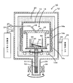
- FIG. 1 is an explanatory view (cross-sectional view) showing the overall configuration of the crystal plate manufacturing apparatus 10.
- the crystal plate manufacturing apparatus 10 includes a pressure vessel 12 that can be evacuated or supplied with pressurized nitrogen gas, and a turntable 30 that can rotate within the pressure vessel 12. And an outer container 42 placed on the turntable 30.
- the pressure vessel 12 is formed in a cylindrical shape whose upper and lower surfaces are discs, and has a heating space 16 surrounded by a heater cover 14 inside.
- the internal temperature of the heating space 16 can be adjusted by an upper heater 18a, a middle heater 18b, and a lower heater 18c arranged in the vertical direction of the side surface of the heater cover 14, and a bottom heater 18d arranged on the bottom surface of the heater cover 14. It has become.
- the heating space 16 has enhanced heat insulation properties by a heater heat insulating material 20 that covers the periphery of the heater cover 14.
- the pressure vessel 12 is connected with a nitrogen gas pipe 24 of a nitrogen gas cylinder 22 and a vacuum drawing pipe 28 of a vacuum pump 26.
- the nitrogen gas pipe 24 passes through the pressure vessel 12, the heater heat insulating material 20, and the heater cover 14 and opens into the heating space 16.
- the nitrogen gas pipe 24 is branched in the middle and is also opened in the gap between the pressure vessel 12 and the heater heat insulating material 20.
- a mass flow controller 25 capable of adjusting the flow rate is attached to a branch pipe communicating with the inside of the heating space 16 in the nitrogen gas pipe 24.
- the evacuation pipe 28 penetrates the pressure vessel 12 and opens in a gap between the pressure vessel 12 and the heater heat insulating material 20.
- the turntable 30 is formed in a disk shape and is disposed below the heating space 16.
- a rotating shaft 34 having an internal magnet 32 is attached to the lower surface of the turntable 30.
- the rotating shaft 34 passes through the heater cover 14 and the heater heat insulating material 20 and is inserted into a cylindrical casing 36 integrated with the lower surface of the pressure vessel 12.
- a cylindrical external magnet 38 is rotatably disposed on the outer periphery of the casing 36 by a motor (not shown).
- the external magnet 38 faces the internal magnet 32 of the rotating shaft 34 through the casing 36. For this reason, as the external magnet 38 rotates, the rotary shaft 34 having the internal magnet 32 rotates, and as a result, the turntable 30 rotates. Further, as the external magnet 38 moves up and down, the rotating shaft 34 having the internal magnet 32 moves up and down, and as a result, the turntable 30 moves up and down.
- the outer container 42 has a bottomed cylindrical metal outer container body 44 and a metal outer container lid 46 that closes the upper opening of the outer container body 44.
- a nitrogen introduction pipe 48 is attached to the outer container lid 46 obliquely upward from the center of the lower surface.
- the nitrogen introduction pipe 48 is designed so that it does not collide with the nitrogen gas pipe 24 even if the outer container 42 rotates and comes closest to the nitrogen gas pipe 24 as the turntable 30 rotates. Specifically, the distance between the two when the nitrogen introduction pipe 48 is closest to the nitrogen gas pipe 24 is set to several mm to several cm.
- a growing container 50 made of alumina having a bottomed cylindrical shape is disposed inside the outer container main body 44.
- a disc-shaped alumina seed crystal substrate tray 52 is disposed in the growth container 50.
- This seed crystal substrate tray 52 has a recess for fitting a disc-shaped seed crystal substrate 54 at the center, one end is placed on the tray base 56, and the other end is in contact with the bottom surface of the growth vessel 50.
- the seed crystal substrate 54 may be a sapphire substrate having the same type of thin film as the group 3B nitride formed thereon, or may be the same type of substrate as the group 3B nitride.
- the 3B group metal and the flux are accommodated in the growth container 50. The flux may be appropriately selected from various metals according to the type of the group 3B metal.
- the group 3B metal is gallium, an alkali metal is preferable, metal sodium or metal potassium is more preferable, and metal sodium is preferable. Further preferred.
- the group 3B metal or flux becomes a mixed melt by heating.
- the outer container 42 and the growth container 50 are arranged so as to be coaxial with the rotation center of the turntable 30. For this reason, during rotation, the mixed melt in the growth vessel 50 rotates in the horizontal direction and does not shake significantly in the vertical direction.
- This crystal plate manufacturing apparatus 10 is used for manufacturing a group 3B nitride by a flux method.
- a gallium nitride crystal plate is manufactured as the group 3B nitride crystal plate
- a GaN template is prepared as the seed crystal substrate 54, metal gallium as the group 3B metal, and metal sodium as the flux.
- the seed crystal substrate 54 is immersed in a mixed melt containing metallic gallium and metallic sodium in the growth vessel 50, and the rotating base 30 is rotated and the heating space 16 is heated by the heaters 18a to 18d and the mixed melt is pressurized.
- gallium nitride crystals are grown on the seed crystal substrate 54 in the mixed melt. It is preferable to add an appropriate amount of carbon to the mixed melt because generation of miscellaneous crystals is suppressed.
- the miscellaneous crystal means gallium nitride crystallized in a place other than the seed crystal substrate 54.
- Inclusion is a solidification of a mixed melt (melt of metal gallium and metal sodium) taken into a crystal of gallium nitride.
- the inclusion content ratio is an occupancy ratio of the area of the black portion of the binary image obtained by performing binarization processing on the image taken after polishing the plate surface of the gallium nitride crystal plate.
- the heating temperature is preferably set to 700 to 1000 ° C., more preferably 800 to 900 ° C.
- the upper heater 18a, the middle heater 18b, the lower heater 18c, and the bottom heater 18d are set to increase in temperature in this order, or the upper heater 18a and the middle heater 18b are set to the same temperature T1.
- the lower heater 18c and the bottom heater 18d are set to a temperature T2 higher than the temperature T1.
- the pressure of the pressurized nitrogen gas is preferably set to 1 to 7 MPa, more preferably 2 to 6 MPa.
- the vacuum pump 26 is driven and the internal pressure of the pressure-resistant vessel 12 is set to a high vacuum state (for example, 1 Pa or less or 0.1 Pa or less) through the vacuuming pipe 28. Thereafter, the vacuuming pipe 28 is closed by a valve (not shown), and nitrogen gas is supplied from the nitrogen gas cylinder 22 to the inside and outside of the heater cover 14 through the nitrogen gas pipe 24.
- the nitrogen gas is supplied to the heating space 16 by the mass flow controller 25. Continue to supply at a flow rate.
- the branch pipe that communicates with the outside of the heater cover 14 in the nitrogen gas pipe 24 is closed by a valve (not shown).
- the growth vessel 50 in which the seed crystal substrate 54 is immersed in the mixed melt is rotated so that the crystal growth rate of gallium nitride on the seed crystal substrate 54 is 5 to 25 ⁇ m / h, preferably 10 to 25 ⁇ m / h.
- the crystal growth rate is less than 5 ⁇ m / h, the crystal growth time becomes excessive, making it difficult to actually manufacture, and if the crystal growth rate exceeds 25 ⁇ m / h, the inclusion content tends to increase, which is not preferable.
- the reversing operation of rotating in one direction without being reversed, rotating in one direction for 1 minute or more and then rotating in the reverse direction for 1 minute or more is repeated, or 5 in one direction.
- the growth time of the gallium nitride crystal may be appropriately set according to the heating temperature and the pressure of the pressurized nitrogen gas, and may be set in the range of several hours to several hundred hours, for example.
- the crystal plate manufacturing apparatus 10 of the present embodiment nitrogen gas is introduced at a high temperature while gently rotating the growth vessel 50 containing the mixed melt in the sealed pressure vessel 12.
- a group 3B nitride crystal having an inclusion content of 10% or less, preferably 2% or less is obtained.
- various technical fields in which the Group 3B nitride crystal is required to have high quality for example, a high color rendering white LED called a post fluorescent lamp, a blue-violet laser disk for high-speed and high-density optical memory, and a hybrid vehicle It can be used for power devices used in inverters.
- the seed crystal substrate tray 52 with the seed crystal substrate 54 fitted in the center is used and one end of the seed crystal substrate tray 52 is placed on the tray table 56 and is tilted in the growth container 50, the entire surface of the seed crystal substrate 54 is disposed. In this case, crystal growth is easy to proceed. Since the mixed melt is likely to stagnate at the peripheral edge of the bottom surface of the growth vessel 50, if a part of the seed crystal substrate 54 is located in the vicinity thereof, the crystal growth of that part tends to be insufficient. However, in this embodiment, since the seed crystal substrate tray 52 is used, the seed crystal substrate 54 is not positioned near the bottom edge of the growth vessel 50, and crystal growth proceeds sufficiently on the entire surface of the seed crystal substrate 54. It is.
- the pipe 24 and the pipe 48 do not prevent the outer container 42 from rotating together with the turntable 30.
- the entire heating space 16 can be maintained at a uniform temperature including the vicinity of the bottom surface where the temperature is likely to be non-uniform. .
- the rotating shaft 34 integrated with the internal magnet 32 rotates and moves up and down as the external magnet 38 arranged on the outer periphery of the casing 36 rotates and moves up and down, the inside of the pressure vessel 12 is moved.
- the outer container 42 can be rotated and moved up and down while being kept sealed.
- Example 1 A gallium nitride crystal plate was produced using the crystal plate manufacturing apparatus 10 shown in FIG. The procedure will be described in detail below. First, in a glove box in an argon atmosphere, a tray base 56 is placed at one end of a growth container 50 having an inner diameter of ⁇ 100 mm, and the seed crystal substrate tray 52 is leaned against the tray base 56 so that the angle becomes 10 °. A ⁇ 3 inch GaN template was placed as a seed crystal substrate 54 in the center of the seed crystal substrate tray 52. Further, 110 g of metallic sodium, 130 g of metallic gallium, and 300 mg of carbon were filled in the growth vessel 50.
- the growing container 50 was placed in the outer container body 44, and the opening of the outer container body 44 was closed with an outer container lid 46 with a nitrogen introduction pipe 48.
- the outer container 42 was placed on a turntable 30 that had been vacuum-baked in advance, and the pressure-resistant container 12 was sealed with a lid (not shown).
- the inside of the pressure vessel 12 was evacuated to 0.1 Pa or less by driving the vacuum pump 26.
- the upper heater 18a, the middle heater 18b, the lower heater 18c, and the bottom heater 18d are adjusted to 855 ° C., 855 ° C., 880 ° C., and 880 ° C., respectively, and the temperature of the heating space 16 is heated to 870 ° C.
- the nitrogen gas was introduced from the nitrogen gas cylinder 22 up to 4.5 MPa, and the outer container 42 was rotated around the central axis at a speed of 30 rpm. And it hold
- the gallium nitride crystal plate had a size of ⁇ 3 inch, a thickness of about 1.5 mm, and a crystal growth rate of about 10 ⁇ m / h.
- the gallium nitride crystal plate is polished to a thickness of 500 ⁇ m, the photographed image is binarized, and the inclusion area in the 70% region excluding the outer peripheral portion of the seed crystal substrate 54 (binary image) The area of the black portion) was determined, and the ratio of the area of inclusion to the entire 70% region, that is, the inclusion content was calculated.
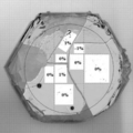
- FIG. 2 is a photograph of the gallium nitride crystal plate of Example 1. This photograph is a composite photograph in which fragments obtained after polishing on the photograph before polishing of the obtained gallium nitride crystal plate are returned to their original positions.
- a circle indicated by a dotted line in the photograph represents a 70% region boundary excluding the outer periphery of the seed crystal substrate, and this region is divided into upper, middle, and lower regions among nine divided regions divided by two vertical and horizontal line segments.
- the inclusion content for each of the five left and right was indicated by a numerical value. As is apparent from FIG. 2, the inclusion content was 0 to 10%.
- the dislocation density was 3 ⁇ 10 4 pieces / cm 2 .
- Example 2 A gallium nitride crystal was grown under the same conditions as in Example 1. However, the rotational speed of the outer container 42 was 1 rpm. The obtained gallium nitride crystal plate had a size of ⁇ 3 inches, a thickness of about 750 ⁇ m, and a crystal growth rate of about 5 ⁇ m / h. Also for this gallium nitride crystal plate, the inclusion content of the five divided regions was measured in the same manner as in Example 1, and it was 0 to 10%. When irradiated with light from a mercury lamp, it emitted blue fluorescence. Further, the dislocation density was 1 ⁇ 10 4 cells / cm 2.
- Example 3 A gallium nitride crystal was grown under the same conditions as in Example 1. However, the rotation speed of the outer container 42 was 5 rpm. The obtained gallium nitride crystal plate had a size of ⁇ 3 inch, a thickness of about 1 mm, and a crystal growth rate of about 7 ⁇ m / h. Also for this gallium nitride crystal plate, the inclusion content of the five divided regions was measured in the same manner as in Example 1, and it was 0 to 1%. When irradiated with light from a mercury lamp, it emitted blue fluorescence. Furthermore, the dislocation density was 2 ⁇ 10 4 pieces / cm 2 .
- Example 4 A gallium nitride crystal was grown under the same conditions as in Example 1. However, the seed crystal substrate tray 52 was not used, and the seed crystal substrate 54 was directly placed on the tray table 56.
- the seed crystal substrate 54 was a ⁇ 2 inch GaN template
- the growth vessel 50 was an alumina vessel with an inner diameter ⁇ 70 mm
- the growth vessel 50 was filled with 60 g of metallic sodium, 40 g of metallic gallium, and 150 mg of carbon.
- the rotation speed of the outer container 42 was 15 rpm.
- the obtained gallium nitride crystal plate had a size of ⁇ 2 inches, a thickness of about 1.5 mm, and a crystal growth rate of about 10 ⁇ m / h.
- Example 3 is a photograph of the gallium nitride crystal plate of Example 4. Also for this gallium nitride crystal plate, the inclusion content of the five divided regions was measured in the same manner as in Example 1, and it was 0 to 1%. When irradiated with light from a mercury lamp, it emitted blue fluorescence.
- Example 5 A gallium nitride crystal was grown under the same conditions as in Example 4. However, the rotational speed of the outer container 42 was 60 rpm. The obtained gallium nitride crystal plate had a size of ⁇ 2 inches, a thickness of about 1.5 mm, and a crystal growth rate of about 10 ⁇ m / h. Also for this gallium nitride crystal plate, the inclusion content of the five divided regions was measured in the same manner as in Example 1, and it was 0 to 5%. When irradiated with light from a mercury lamp, it emitted blue fluorescence.
- Example 6 A gallium nitride crystal was grown under the same conditions as in Example 4. However, the rotational speed of the outer container 42 was 100 rpm. The obtained gallium nitride crystal plate had a size of ⁇ 2 inches, a thickness of about 1.5 mm, and a crystal growth rate of about 10 ⁇ m / h. Also for this gallium nitride crystal plate, the inclusion content of the five divided regions was measured in the same manner as in Example 1, and it was 0 to 10%. When irradiated with light from a mercury lamp, it emitted blue fluorescence.
- Example 7 A gallium nitride crystal was grown under the same conditions as in Example 4. However, the rotational speed of the outer container 42 was reversed every 5 minutes at 30 rpm. The size of the obtained gallium nitride crystal plate was ⁇ 2 inches, the thickness was about 2 mm, and the crystal growth rate was about 13 ⁇ m / h.
- FIG. 4 is a photograph of the gallium nitride crystal plate of Example 7. Also for this gallium nitride crystal plate, the inclusion content of the five divided regions was measured in the same manner as in Example 1, and it was 0 to 1%. When irradiated with light from a mercury lamp, it emitted blue fluorescence. Furthermore, the dislocation density was 5 ⁇ 10 4 pieces / cm 2 .
- Example 8 A gallium nitride crystal was grown under the same conditions as in Example 7. However, the rotation speed of the outer container 42 was reversed every 3 minutes at 30 rpm. The size of the obtained gallium nitride crystal plate was ⁇ 2 inches, the thickness was about 2.5 mm, and the crystal growth rate was about 17 ⁇ m / h. Also for this gallium nitride crystal plate, the inclusion content of the five divided regions was measured in the same manner as in Example 1, and it was 0 to 1%. When irradiated with light from a mercury lamp, it emitted blue fluorescence.
- Example 9 A gallium nitride crystal was grown under the same conditions as in Example 7. However, the rotational speed of the outer container 42 was reversed every minute at 30 rpm. The size of the obtained gallium nitride crystal plate was ⁇ 2 inches, the thickness was about 3.8 mm, and the crystal growth rate was about 25 ⁇ m / h. Also for this gallium nitride crystal plate, the inclusion content of the five divided regions was measured in the same manner as in Example 1, and it was 0 to 10%. When irradiated with light from a mercury lamp, it emitted blue fluorescence.
- Example 10 A gallium nitride crystal was grown under the same conditions as in Example 7. However, the outer container 42 was rotated at a rotational speed of 30 rpm for 5 seconds, then stopped for 1 second, and then repeated intermittently for 5 seconds in the same direction. The size of the obtained gallium nitride crystal plate was ⁇ 2 inches, the thickness was about 3 mm, and the crystal growth rate was about 20 ⁇ m / h. Also for this gallium nitride crystal plate, the inclusion content of the five divided regions was measured in the same manner as in Example 1, and it was 0 to 5%. When irradiated with light from a mercury lamp, it emitted blue fluorescence.
- FIG. 5 is a photograph of the gallium nitride crystal plate of Comparative Example 1. Also for this gallium nitride crystal plate, the inclusion content of the five divided regions was measured in the same manner as in Example 1, and it was 0 to 42%. The dislocation density was 5 ⁇ 10 4 pieces / cm 2 .
- FIG. 6 is a photograph of the gallium nitride crystal plate of Comparative Example 2.
- the inclusion content of the five divided regions was measured in the same manner as in Example 1, and it was 6 to 30%.
- the dislocation density was 1 ⁇ 10 5 pieces / cm 2 .
- Example 3 A gallium nitride crystal was grown under the same conditions as in Example 10. However, the outer container 42 was rotated for 3 seconds at a rotation speed of 30 rpm, then stopped for 1 second, and then repeated intermittent motion for 3 seconds in the same direction. The crystal growth time was 100 hours. The size of the obtained gallium nitride crystal plate was ⁇ 2 inches, the thickness was about 3 mm, and the crystal growth rate was about 30 ⁇ m / h. Also for this gallium nitride crystal plate, the inclusion content of the five divided regions was measured in the same manner as in Example 1, and it was 0 to 20%. When irradiated with light from a mercury lamp, it emitted blue fluorescence. Furthermore, the dislocation density was 1 ⁇ 10 5 pieces / cm 2 .
- Example 1 The crystal growth conditions and results of Examples 1 to 10 and Comparative Examples 1 to 3 are shown in Table 1.
- Table 1 the inclusion content in Examples 1 to 10 (with rotation) could be suppressed to 10% or less as compared with Comparative Example 1 (without rotation).
- Comparative Example 2 Reversed every 15 seconds at 30 rpm
- the inclusion content was high in spite of the rotation, but this was too mixed in the depth direction (vertical direction) of the mixed melt and crystal growth occurred. This is probably due to the speed becoming too fast.
- Examples 7 to 9 (reversed every 5 to 1 minutes at 30 rpm), although it is reversed, the period is long, so the crystal growth rate is moderated and the inclusion content is considered to be low.
- Example 3 In Comparative Example 3 (intermittent operation every 30 seconds at 30 rpm), the inclusion content was high despite being rotated, but this was too mixed in the depth direction (vertical direction) of the mixed melt. This is thought to be due to the growth rate becoming too fast. On the other hand, in Example 10 (intermittent operation every 5 seconds), the intermittent period is long, so that the crystal growth rate is moderated and the inclusion content is low.
- the present invention can be used for semiconductor devices such as blue LEDs, white LEDs, and blue-violet semiconductor lasers in addition to high-frequency devices represented by power amplifiers.
Landscapes
- Chemical & Material Sciences (AREA)
- Engineering & Computer Science (AREA)
- Crystallography & Structural Chemistry (AREA)
- Materials Engineering (AREA)
- Metallurgy (AREA)
- Organic Chemistry (AREA)
- Inorganic Chemistry (AREA)
- Crystals, And After-Treatments Of Crystals (AREA)
- Liquid Deposition Of Substances Of Which Semiconductor Devices Are Composed (AREA)
Abstract
Description
図1に示す結晶板製造装置10を用いて、窒化ガリウム結晶板を作製した。以下、その手順を詳説する。まず、アルゴン雰囲気のグローブボックス内で、内径φ100mmの育成容器50内の一端にトレー台56を置き、種結晶基板トレー52をトレー台56に立て掛けて角度が10°になるよう育成容器50の底面中央に斜めに置き、その種結晶基板トレー52の中央に種結晶基板54としてφ3インチGaNテンプレートを配置した。さらに金属ナトリウム110g、金属ガリウム130g、炭素300mgを育成容器50内に充填した。この育成容器50を外容器本体44内に入れ、外容器本体44の開口を窒素導入パイプ48の付いた外容器蓋46で閉じた。この外容器42を、予め真空ベークしてある回転台30の上に設置し、耐圧容器12に蓋(図示せず)をして密閉した。
実施例1と同様の条件で窒化ガリウム結晶の育成を行った。但し、外容器42の回転速度は1rpmとした。得られた窒化ガリウム結晶板の大きさはφ3インチであり、厚さは約750μmであり、結晶成長速度は約5μm/hであった。この窒化ガリウム結晶板についても実施例1と同様にして5つの分割領域のインクルージョン含有率を測定したところ、0~10%であった。また、水銀ランプの光を照射したところ、青色の蛍光を発した。更に、転位密度は1×104個/cm2であった。
実施例1と同様の条件で窒化ガリウム結晶の育成を行った。但し、外容器42の回転速度は5rpmとした。得られた窒化ガリウム結晶板の大きさはφ3インチであり、厚さは約1mmであり、結晶成長速度は約7μm/hであった。この窒化ガリウム結晶板についても実施例1と同様にして5つの分割領域のインクルージョン含有率を測定したところ、0~1%であった。また、水銀ランプの光を照射したところ、青色の蛍光を発した。更に、転位密度は2×104個/cm2であった。
実施例1と同様の条件で窒化ガリウム結晶の育成を行った。但し、種結晶基板トレー52は用いず、種結晶基板54を直接トレー台56に載せた。また、種結晶基板54はφ2インチGaNテンプレートを用い、育成容器50は内径φ70mmのアルミナ容器を用い、金属ナトリウム60g、金属ガリウム40g、炭素150mgを育成容器50内に充填した。外容器42の回転速度は15rpmとした。得られた窒化ガリウム結晶板の大きさはφ2インチであり、厚さは約1.5mmであり、結晶成長速度は約10μm/hであった。図3は、実施例4の窒化ガリウム結晶板の写真である。この窒化ガリウム結晶板についても実施例1と同様にして5つの分割領域のインクルージョン含有率を測定したところ、0~1%であった。また、水銀ランプの光を照射したところ、青色の蛍光を発した。
実施例4と同様の条件で窒化ガリウム結晶の育成を行った。但し、外容器42の回転速度は60rpmとした。得られた窒化ガリウム結晶板の大きさはφ2インチであり、厚さは約1.5mmであり、結晶成長速度は約10μm/hであった。この窒化ガリウム結晶板についても実施例1と同様にして5つの分割領域のインクルージョン含有率を測定したところ、0~5%であった。また、水銀ランプの光を照射したところ、青色の蛍光を発した。
実施例4と同様の条件で窒化ガリウム結晶の育成を行った。但し、外容器42の回転速度は100rpmとした。得られた窒化ガリウム結晶板の大きさはφ2インチであり、厚さは約1.5mmであり、結晶成長速度は約10μm/hであった。この窒化ガリウム結晶板についても実施例1と同様にして5つの分割領域のインクルージョン含有率を測定したところ、0~10%であった。また、水銀ランプの光を照射したところ、青色の蛍光を発した。
実施例4と同様の条件で窒化ガリウム結晶の育成を行った。但し、外容器42の回転速度は30rpmで5分毎に反転させた。得られた窒化ガリウム結晶板の大きさはφ2インチであり、厚さは約2mmであり、結晶成長速度は約13μm/hであった。図4は、実施例7の窒化ガリウム結晶板の写真である。この窒化ガリウム結晶板についても実施例1と同様にして5つの分割領域のインクルージョン含有率を測定したところ、0~1%であった。また、水銀ランプの光を照射したところ、青色の蛍光を発した。更に、転位密度は5×104個/cm2であった。
実施例7と同様の条件で窒化ガリウム結晶の育成を行った。但し、外容器42の回転速度は30rpmで3分毎に反転させた。得られた窒化ガリウム結晶板の大きさはφ2インチであり、厚さは約2.5mmであり、結晶成長速度は約17μm/hであった。この窒化ガリウム結晶板についても実施例1と同様にして5つの分割領域のインクルージョン含有率を測定したところ、0~1%であった。また、水銀ランプの光を照射したところ、青色の蛍光を発した。
実施例7と同様の条件で窒化ガリウム結晶の育成を行った。但し、外容器42の回転速度は30rpmで1分毎に反転させた。得られた窒化ガリウム結晶板の大きさはφ2インチであり、厚さは約3.8mmであり、結晶成長速度は約25μm/hであった。この窒化ガリウム結晶板についても実施例1と同様にして5つの分割領域のインクルージョン含有率を測定したところ、0~10%であった。また、水銀ランプの光を照射したところ、青色の蛍光を発した。
実施例7と同様の条件で窒化ガリウム結晶の育成を行った。但し、外容器42は回転速度30rpmで5秒回転しそののち1秒停止しそののち同方向に5秒回転させる間欠運動を繰り返した。得られた窒化ガリウム結晶板の大きさはφ2インチであり、厚さは約3mmであり、結晶成長速度は約20μm/hであった。この窒化ガリウム結晶板についても実施例1と同様にして5つの分割領域のインクルージョン含有率を測定したところ、0~5%であった。また、水銀ランプの光を照射したところ、青色の蛍光を発した。
実施例4と同様の条件で窒化ガリウム結晶の育成を行った。但し、外容器42は回転させなかった。得られた窒化ガリウム結晶の大きさはφ2インチであり、厚さは約1.5mmであり、結晶成長速度は約10μm/hであり、色は部分的に褐色に着色していた。図5は、比較例1の窒化ガリウム結晶板の写真である。この窒化ガリウム結晶板についても実施例1と同様にして5つの分割領域のインクルージョン含有率を測定したところ、0~42%であった。また、転位密度は5×104個/cm2であった。
実施例1と同様の条件で窒化ガリウム結晶の育成を行った。但し、外容器42の回転速度は30rpmで15秒毎に反転させ、結晶育成時間は100時間とした。得られた窒化ガリウム結晶の大きさはφ3インチであり、厚さは約3mmであり、結晶成長速度は約30μm/hであった。図6は、比較例2の窒化ガリウム結晶板の写真である。この窒化ガリウム結晶板についても実施例1と同様にして5つの分割領域のインクルージョン含有率を測定したところ、6~30%であった。また、転位密度は1×105個/cm2であった。
実施例10と同様の条件で窒化ガリウム結晶の育成を行った。但し、外容器42は回転速度30rpmで3秒回転しそののち1秒停止しそののち同方向に3秒回転させる間欠運動を繰り返した。また、結晶育成時間は100時間とした。得られた窒化ガリウム結晶板の大きさはφ2インチであり、厚さは約3mmであり、結晶成長速度は約30μm/hであった。この窒化ガリウム結晶板についても実施例1と同様にして5つの分割領域のインクルージョン含有率を測定したところ、0~20%であった。また、水銀ランプの光を照射したところ、青色の蛍光を発した。更に、転位密度は1×105個/cm2であった。

Claims (8)
- 3B族金属とフラックスとを含む融液から窒素含有ガスの存在下で種結晶基板上に3B族窒化物結晶を生成させた3B族窒化物結晶板であって、
前記種結晶基板のうち外周部を除く全面積の70%の領域に生成した3B族窒化物結晶のインクルージョンの含有率が10%以下である、
3B族窒化物結晶板。 - 前記インクルージョンの含有率が2%以下である、
請求項1に記載の3B族窒化物結晶板。 - 前記インクルージョンが少なくとも前記フラックスを含む成分からなる、
請求項1又は2に記載の3B族窒化物結晶板。 - 前記インクルージョンの含有率は、板面を研磨加工したあと撮影した画像に2値化処理を施すことにより得られる2値画像の黒色部分の面積の占有率である、
請求項1~3のいずれか1項に記載の3B族窒化物結晶板。 - 前記3B族窒化物は、窒化ガリウムである、
請求項1~4のいずれか1項に記載の3B族窒化物結晶板。 - 前記フラックスは、少なくともナトリウムを含む金属融液である、
請求項1~5のいずれか1項に記載の3B族窒化物結晶板。 - 転位密度が105個/cm2以下である、
請求項1~6のいずれか1項に記載の3B族窒化物結晶板。 - 水銀ランプの光を照射したときに青色の蛍光を発する、
請求項1~7のいずれか1項に記載の3B族窒化物結晶板。
Priority Applications (3)
| Application Number | Priority Date | Filing Date | Title |
|---|---|---|---|
| CN200980154840.0A CN102282299B (zh) | 2009-01-21 | 2009-12-14 | 13族氮化物晶板 |
| JP2010547408A JP5688294B2 (ja) | 2009-01-21 | 2009-12-14 | 3b族窒化物結晶板 |
| US13/135,829 US9677192B2 (en) | 2009-01-21 | 2011-07-15 | Group 3B nitride crystal substrate |
Applications Claiming Priority (4)
| Application Number | Priority Date | Filing Date | Title |
|---|---|---|---|
| JP2009011264 | 2009-01-21 | ||
| JP2009-011264 | 2009-01-21 | ||
| JP2009017289 | 2009-01-28 | ||
| JP2009-017289 | 2009-01-28 |
Related Child Applications (1)
| Application Number | Title | Priority Date | Filing Date |
|---|---|---|---|
| US13/135,829 Continuation US9677192B2 (en) | 2009-01-21 | 2011-07-15 | Group 3B nitride crystal substrate |
Publications (1)
| Publication Number | Publication Date |
|---|---|
| WO2010084675A1 true WO2010084675A1 (ja) | 2010-07-29 |
Family
ID=42355741
Family Applications (2)
| Application Number | Title | Priority Date | Filing Date |
|---|---|---|---|
| PCT/JP2009/070827 Ceased WO2010084675A1 (ja) | 2009-01-21 | 2009-12-14 | 3b族窒化物結晶板 |
| PCT/JP2009/070828 Ceased WO2010084676A1 (ja) | 2009-01-21 | 2009-12-14 | 3b族窒化物結晶板製造装置 |
Family Applications After (1)
| Application Number | Title | Priority Date | Filing Date |
|---|---|---|---|
| PCT/JP2009/070828 Ceased WO2010084676A1 (ja) | 2009-01-21 | 2009-12-14 | 3b族窒化物結晶板製造装置 |
Country Status (4)
| Country | Link |
|---|---|
| US (1) | US9677192B2 (ja) |
| JP (3) | JP5688294B2 (ja) |
| CN (1) | CN102282299B (ja) |
| WO (2) | WO2010084675A1 (ja) |
Cited By (8)
| Publication number | Priority date | Publication date | Assignee | Title |
|---|---|---|---|---|
| WO2013022123A1 (ja) * | 2011-08-10 | 2013-02-14 | 日本碍子株式会社 | 半導体発光素子およびこれを含む積層体 |
| WO2015012218A1 (ja) * | 2013-07-22 | 2015-01-29 | 日本碍子株式会社 | 複合基板、その製造方法、機能素子および種結晶基板 |
| US9041004B2 (en) | 2011-08-10 | 2015-05-26 | Ngk Insulators, Ltd. | Films of nitrides of group 13 elements and layered body including the same |
| US9045844B2 (en) | 2011-08-10 | 2015-06-02 | Ngk Insulators, Ltd. | Method for peeling group 13 element nitride film |
| US9196480B2 (en) | 2013-03-29 | 2015-11-24 | Ngk Insulators, Ltd. | Method for treating group III nitride substrate and method for manufacturing epitaxial substrate |
| KR20160015244A (ko) | 2013-06-06 | 2016-02-12 | 엔지케이 인슐레이터 엘티디 | 13족 질화물 복합 기판, 반도체 소자, 및 13족 질화물 복합 기판의 제조 방법 |
| CN106367804A (zh) * | 2016-10-28 | 2017-02-01 | 北京大学东莞光电研究院 | 一种压强调控晶体生长反应釜 |
| JP2021157763A (ja) * | 2020-03-27 | 2021-10-07 | 住友金属鉱山株式会社 | 粒子の連結態様の評価方法 |
Families Citing this family (9)
| Publication number | Priority date | Publication date | Assignee | Title |
|---|---|---|---|---|
| WO2010053960A1 (en) * | 2008-11-07 | 2010-05-14 | The Regents Of The University Of California | Using boron-containing compounds, gasses and fluids during ammonothermal growth of group-iii nitride crystals |
| JP6175817B2 (ja) * | 2013-03-13 | 2017-08-09 | 株式会社リコー | 13族窒化物結晶の製造方法、及び製造装置 |
| WO2015047816A1 (en) | 2013-09-30 | 2015-04-02 | Gt Crystal Systems, Llc | Method of automatically measuring seed melt back of crystalline material |
| WO2016084492A1 (ja) | 2014-11-26 | 2016-06-02 | 日本碍子株式会社 | 13族元素窒化物結晶の製造方法および装置 |
| CN105648533A (zh) * | 2016-03-12 | 2016-06-08 | 东莞市中镓半导体科技有限公司 | 液相生长氮化镓晶体的装置 |
| CN109680334A (zh) * | 2019-03-07 | 2019-04-26 | 中国电子科技集团公司第四十六研究所 | 一种钠助熔剂法氮化镓单晶的生长装置 |
| JP7349705B2 (ja) * | 2019-07-01 | 2023-09-25 | 国立研究開発法人理化学研究所 | レーザ加工装置 |
| WO2023188575A1 (ja) * | 2022-03-28 | 2023-10-05 | 日本碍子株式会社 | Iii族元素窒化物基板およびiii族元素窒化物基板の製造方法 |
| WO2023188574A1 (ja) * | 2022-03-28 | 2023-10-05 | 日本碍子株式会社 | Iii族元素窒化物基板およびiii族元素窒化物基板の製造方法 |
Citations (7)
| Publication number | Priority date | Publication date | Assignee | Title |
|---|---|---|---|---|
| JP2005263622A (ja) * | 2004-02-19 | 2005-09-29 | Matsushita Electric Ind Co Ltd | 化合物単結晶の製造方法、およびそれに用いる製造装置 |
| WO2005111278A1 (ja) * | 2004-05-19 | 2005-11-24 | Sumitomo Electric Industries, Ltd. | Iii族窒化物半導体結晶およびその製造方法ならびにiii族窒化物半導体デバイス |
| JP2006290671A (ja) * | 2005-04-08 | 2006-10-26 | Hitachi Cable Ltd | Iii−v族窒化物半導体結晶の製造方法 |
| JP2007119325A (ja) * | 2005-10-31 | 2007-05-17 | Sumitomo Electric Ind Ltd | Iii族窒化物結晶およびその成長方法 |
| JP2007217227A (ja) * | 2006-02-16 | 2007-08-30 | Sumitomo Electric Ind Ltd | GaN結晶の製造方法、GaN結晶基板および半導体デバイス |
| JP2007238343A (ja) * | 2006-03-06 | 2007-09-20 | Ngk Insulators Ltd | Iii族窒化物単結晶の育成方法 |
| JP2007254161A (ja) * | 2006-03-20 | 2007-10-04 | Ngk Insulators Ltd | Iii族窒化物結晶の製造方法およびiii族窒化物結晶の製造装置 |
Family Cites Families (20)
| Publication number | Priority date | Publication date | Assignee | Title |
|---|---|---|---|---|
| JPH05152416A (ja) * | 1991-11-26 | 1993-06-18 | Shinko Electric Co Ltd | 表面処理装置の搬送装置 |
| JPH0687688A (ja) * | 1992-03-31 | 1994-03-29 | Ulvac Japan Ltd | 分子線エピタキシー装置 |
| JPH08310895A (ja) * | 1995-05-10 | 1996-11-26 | Nissin Electric Co Ltd | 分子線エピタキシー装置の基板シャッタ機構 |
| TW385493B (en) | 1997-08-04 | 2000-03-21 | Sumitomo Chemical Co | Method for manufacturing group III-V compound semiconductor |
| JP3603598B2 (ja) * | 1997-08-04 | 2004-12-22 | 住友化学株式会社 | 3−5族化合物半導体の製造方法 |
| US7097707B2 (en) * | 2001-12-31 | 2006-08-29 | Cree, Inc. | GaN boule grown from liquid melt using GaN seed wafers |
| US7063741B2 (en) * | 2002-03-27 | 2006-06-20 | General Electric Company | High pressure high temperature growth of crystalline group III metal nitrides |
| AU2003246117A1 (en) * | 2002-07-31 | 2004-02-23 | Osaka Industrial Promotion Organization | Method for producing group iii element nitride single crystal and group iii element nitride transparent single crystal prepared thereby |
| US7255742B2 (en) | 2003-07-02 | 2007-08-14 | Matsushita Electric Industrial Co., Ltd. | Method of manufacturing Group III nitride crystals, method of manufacturing semiconductor substrate, Group III nitride crystals, semiconductor substrate, and electronic device |
| JP4554287B2 (ja) * | 2003-07-02 | 2010-09-29 | パナソニック株式会社 | Iii族窒化物結晶の製造方法、および半導体基板の製造方法 |
| WO2005080648A1 (ja) | 2004-02-19 | 2005-09-01 | Matsushita Electric Industrial Co., Ltd. | 化合物単結晶の製造方法、およびそれに用いる製造装置 |
| CN1938457B (zh) * | 2004-03-31 | 2011-11-30 | 日本碍子株式会社 | 氮化镓单晶的生长方法和氮化镓单晶 |
| JP4514584B2 (ja) * | 2004-11-16 | 2010-07-28 | 富士通株式会社 | 化合物半導体装置及びその製造方法 |
| US7897490B2 (en) * | 2005-12-12 | 2011-03-01 | Kyma Technologies, Inc. | Single crystal group III nitride articles and method of producing same by HVPE method incorporating a polycrystalline layer for yield enhancement |
| JP2007201145A (ja) * | 2006-01-26 | 2007-08-09 | Toyoda Gosei Co Ltd | n型III族窒化物系化合物半導体層の成長方法 |
| JP5177555B2 (ja) * | 2006-03-06 | 2013-04-03 | 日本碍子株式会社 | 単結晶の育成方法 |
| JP4787692B2 (ja) * | 2006-07-13 | 2011-10-05 | 株式会社リコー | 結晶成長装置 |
| JP4915563B2 (ja) * | 2006-09-13 | 2012-04-11 | パナソニック株式会社 | 窒化ガリウム系単結晶の育成方法およびそれにより得られる窒化ガリウム系単結晶 |
| JP4830976B2 (ja) * | 2007-05-30 | 2011-12-07 | 豊田合成株式会社 | Iii族窒化物半導体製造装置 |
| JP5261401B2 (ja) * | 2007-12-21 | 2013-08-14 | 日本碍子株式会社 | 窒化物単結晶の育成装置 |
-
2009
- 2009-12-14 WO PCT/JP2009/070827 patent/WO2010084675A1/ja not_active Ceased
- 2009-12-14 WO PCT/JP2009/070828 patent/WO2010084676A1/ja not_active Ceased
- 2009-12-14 JP JP2010547408A patent/JP5688294B2/ja active Active
- 2009-12-14 JP JP2010547409A patent/JP5607548B2/ja active Active
- 2009-12-14 CN CN200980154840.0A patent/CN102282299B/zh active Active
-
2011
- 2011-07-15 US US13/135,829 patent/US9677192B2/en active Active
-
2014
- 2014-08-26 JP JP2014171923A patent/JP5807100B2/ja active Active
Patent Citations (7)
| Publication number | Priority date | Publication date | Assignee | Title |
|---|---|---|---|---|
| JP2005263622A (ja) * | 2004-02-19 | 2005-09-29 | Matsushita Electric Ind Co Ltd | 化合物単結晶の製造方法、およびそれに用いる製造装置 |
| WO2005111278A1 (ja) * | 2004-05-19 | 2005-11-24 | Sumitomo Electric Industries, Ltd. | Iii族窒化物半導体結晶およびその製造方法ならびにiii族窒化物半導体デバイス |
| JP2006290671A (ja) * | 2005-04-08 | 2006-10-26 | Hitachi Cable Ltd | Iii−v族窒化物半導体結晶の製造方法 |
| JP2007119325A (ja) * | 2005-10-31 | 2007-05-17 | Sumitomo Electric Ind Ltd | Iii族窒化物結晶およびその成長方法 |
| JP2007217227A (ja) * | 2006-02-16 | 2007-08-30 | Sumitomo Electric Ind Ltd | GaN結晶の製造方法、GaN結晶基板および半導体デバイス |
| JP2007238343A (ja) * | 2006-03-06 | 2007-09-20 | Ngk Insulators Ltd | Iii族窒化物単結晶の育成方法 |
| JP2007254161A (ja) * | 2006-03-20 | 2007-10-04 | Ngk Insulators Ltd | Iii族窒化物結晶の製造方法およびiii族窒化物結晶の製造装置 |
Cited By (19)
| Publication number | Priority date | Publication date | Assignee | Title |
|---|---|---|---|---|
| CN103890980A (zh) * | 2011-08-10 | 2014-06-25 | 日本碍子株式会社 | 半导体发光元件以及包含该半导体发光元件的叠层体 |
| WO2013022123A1 (ja) * | 2011-08-10 | 2013-02-14 | 日本碍子株式会社 | 半導体発光素子およびこれを含む積層体 |
| US9041004B2 (en) | 2011-08-10 | 2015-05-26 | Ngk Insulators, Ltd. | Films of nitrides of group 13 elements and layered body including the same |
| US9045844B2 (en) | 2011-08-10 | 2015-06-02 | Ngk Insulators, Ltd. | Method for peeling group 13 element nitride film |
| US9196480B2 (en) | 2013-03-29 | 2015-11-24 | Ngk Insulators, Ltd. | Method for treating group III nitride substrate and method for manufacturing epitaxial substrate |
| US9882042B2 (en) | 2013-06-06 | 2018-01-30 | Ngk Insulators, Ltd. | Group 13 nitride composite substrate semiconductor device, and method for manufacturing group 13 nitride composite substrate |
| KR20160015244A (ko) | 2013-06-06 | 2016-02-12 | 엔지케이 인슐레이터 엘티디 | 13족 질화물 복합 기판, 반도체 소자, 및 13족 질화물 복합 기판의 제조 방법 |
| KR20200033982A (ko) | 2013-06-06 | 2020-03-30 | 엔지케이 인슐레이터 엘티디 | 13족 질화물 복합 기판, 반도체 소자, 및 13족 질화물 복합 기판의 제조 방법 |
| US10347755B2 (en) | 2013-06-06 | 2019-07-09 | Ngk Insulators, Ltd. | Group 13 nitride composite substrate semiconductor device, and method for manufacturing group 13 nitride composite substrate |
| EP3312870A1 (en) | 2013-06-06 | 2018-04-25 | NGK Insulators, Ltd. | Group 13 nitride composite substrate, semiconductor element, and production method for group 13 nitride composite substrate |
| KR101590309B1 (ko) | 2013-07-22 | 2016-01-29 | 엔지케이 인슐레이터 엘티디 | 복합 기판, 그 제조 방법, 기능 소자 및 종결정 기판 |
| WO2015012218A1 (ja) * | 2013-07-22 | 2015-01-29 | 日本碍子株式会社 | 複合基板、その製造方法、機能素子および種結晶基板 |
| JP5805352B2 (ja) * | 2013-07-22 | 2015-11-04 | 日本碍子株式会社 | 複合基板、その製造方法、機能素子および種結晶基板 |
| US10030318B2 (en) | 2013-07-22 | 2018-07-24 | Ngk Insulators, Ltd. | Composite substrate, method for fabricating same, function element, and seed crystal substrate |
| KR20160003289A (ko) | 2013-07-22 | 2016-01-08 | 엔지케이 인슐레이터 엘티디 | 복합 기판, 그 제조 방법, 기능 소자 및 종결정 기판 |
| TWI510667B (zh) * | 2013-07-22 | 2015-12-01 | 日本碍子股份有限公司 | A composite substrate, a manufacturing method thereof, a functional element and a seed crystal substrate |
| CN106367804A (zh) * | 2016-10-28 | 2017-02-01 | 北京大学东莞光电研究院 | 一种压强调控晶体生长反应釜 |
| JP2021157763A (ja) * | 2020-03-27 | 2021-10-07 | 住友金属鉱山株式会社 | 粒子の連結態様の評価方法 |
| JP7543828B2 (ja) | 2020-03-27 | 2024-09-03 | 住友金属鉱山株式会社 | 粒子の連結態様の評価方法 |
Also Published As
| Publication number | Publication date |
|---|---|
| JPWO2010084676A1 (ja) | 2012-07-12 |
| US20110274609A1 (en) | 2011-11-10 |
| US9677192B2 (en) | 2017-06-13 |
| JPWO2010084675A1 (ja) | 2012-07-12 |
| CN102282299A (zh) | 2011-12-14 |
| WO2010084676A1 (ja) | 2010-07-29 |
| JP5607548B2 (ja) | 2014-10-15 |
| JP5688294B2 (ja) | 2015-03-25 |
| JP5807100B2 (ja) | 2015-11-10 |
| JP2015006989A (ja) | 2015-01-15 |
| CN102282299B (zh) | 2014-07-02 |
Similar Documents
| Publication | Publication Date | Title |
|---|---|---|
| JP5688294B2 (ja) | 3b族窒化物結晶板 | |
| JP5244628B2 (ja) | 3b族窒化物結晶板の製法 | |
| JP5451651B2 (ja) | 13族窒化物の結晶成長方法及び13族窒化物結晶 | |
| JP5918749B2 (ja) | 13族元素窒化物膜およびその積層体 | |
| JP5897790B2 (ja) | 3b族窒化物単結晶及びその製法 | |
| JP2011068548A (ja) | Znがドープされた3B族窒化物結晶、その製法及び電子デバイス | |
| JP2016001650A (ja) | 13族元素窒化物結晶層および機能素子 | |
| JP5651481B2 (ja) | 3b族窒化物結晶 | |
| JP6143148B2 (ja) | Iii族窒化物結晶の製造方法および半導体装置の製造方法 | |
| US10538858B2 (en) | Method for manufacturing group 13 nitride crystal and group 13 nitride crystal | |
| JP5651480B2 (ja) | 3b族窒化物結晶の製法 | |
| CN203174224U (zh) | 复合基板以及功能元件 | |
| JP2011020896A (ja) | Znがドープされた3B族窒化物結晶、その製法及び電子デバイス | |
| JP5451085B2 (ja) | 高抵抗材料 | |
| CN203174223U (zh) | 复合基板以及功能元件 |
Legal Events
| Date | Code | Title | Description |
|---|---|---|---|
| WWE | Wipo information: entry into national phase |
Ref document number: 200980154840.0 Country of ref document: CN |
|
| 121 | Ep: the epo has been informed by wipo that ep was designated in this application |
Ref document number: 09838865 Country of ref document: EP Kind code of ref document: A1 |
|
| WWE | Wipo information: entry into national phase |
Ref document number: 2010547408 Country of ref document: JP |
|
| NENP | Non-entry into the national phase |
Ref country code: DE |
|
| 122 | Ep: pct application non-entry in european phase |
Ref document number: 09838865 Country of ref document: EP Kind code of ref document: A1 |