WO2010084587A1 - 色変換膜及び該色変換膜を含む多色発光有機elデバイス - Google Patents
色変換膜及び該色変換膜を含む多色発光有機elデバイス Download PDFInfo
- Publication number
- WO2010084587A1 WO2010084587A1 PCT/JP2009/050880 JP2009050880W WO2010084587A1 WO 2010084587 A1 WO2010084587 A1 WO 2010084587A1 JP 2009050880 W JP2009050880 W JP 2009050880W WO 2010084587 A1 WO2010084587 A1 WO 2010084587A1
- Authority
- WO
- WIPO (PCT)
- Prior art keywords
- dye
- color conversion
- conversion film
- light
- organic
- Prior art date
- Legal status (The legal status is an assumption and is not a legal conclusion. Google has not performed a legal analysis and makes no representation as to the accuracy of the status listed.)
- Ceased
Links
Images


Classifications
-
- G—PHYSICS
- G02—OPTICS
- G02B—OPTICAL ELEMENTS, SYSTEMS OR APPARATUS
- G02B5/00—Optical elements other than lenses
- G02B5/20—Filters
- G02B5/22—Absorbing filters
- G02B5/223—Absorbing filters containing organic substances, e.g. dyes, inks or pigments
-
- C—CHEMISTRY; METALLURGY
- C09—DYES; PAINTS; POLISHES; NATURAL RESINS; ADHESIVES; COMPOSITIONS NOT OTHERWISE PROVIDED FOR; APPLICATIONS OF MATERIALS NOT OTHERWISE PROVIDED FOR
- C09K—MATERIALS FOR MISCELLANEOUS APPLICATIONS, NOT PROVIDED FOR ELSEWHERE
- C09K11/00—Luminescent materials, e.g. electroluminescent or chemiluminescent
- C09K11/06—Luminescent materials, e.g. electroluminescent or chemiluminescent containing organic luminescent materials
-
- G—PHYSICS
- G02—OPTICS
- G02B—OPTICAL ELEMENTS, SYSTEMS OR APPARATUS
- G02B5/00—Optical elements other than lenses
- G02B5/20—Filters
- G02B5/22—Absorbing filters
- G02B5/23—Photochromic filters
-
- H—ELECTRICITY
- H10—SEMICONDUCTOR DEVICES; ELECTRIC SOLID-STATE DEVICES NOT OTHERWISE PROVIDED FOR
- H10K—ORGANIC ELECTRIC SOLID-STATE DEVICES
- H10K50/00—Organic light-emitting devices
- H10K50/10—OLEDs or polymer light-emitting diodes [PLED]
- H10K50/11—OLEDs or polymer light-emitting diodes [PLED] characterised by the electroluminescent [EL] layers
- H10K50/125—OLEDs or polymer light-emitting diodes [PLED] characterised by the electroluminescent [EL] layers specially adapted for multicolour light emission, e.g. for emitting white light
- H10K50/13—OLEDs or polymer light-emitting diodes [PLED] characterised by the electroluminescent [EL] layers specially adapted for multicolour light emission, e.g. for emitting white light comprising stacked EL layers within one EL unit
-
- H—ELECTRICITY
- H10—SEMICONDUCTOR DEVICES; ELECTRIC SOLID-STATE DEVICES NOT OTHERWISE PROVIDED FOR
- H10K—ORGANIC ELECTRIC SOLID-STATE DEVICES
- H10K59/00—Integrated devices, or assemblies of multiple devices, comprising at least one organic light-emitting element covered by group H10K50/00
- H10K59/30—Devices specially adapted for multicolour light emission
- H10K59/38—Devices specially adapted for multicolour light emission comprising colour filters or colour changing media [CCM]
-
- H—ELECTRICITY
- H10—SEMICONDUCTOR DEVICES; ELECTRIC SOLID-STATE DEVICES NOT OTHERWISE PROVIDED FOR
- H10K—ORGANIC ELECTRIC SOLID-STATE DEVICES
- H10K59/00—Integrated devices, or assemblies of multiple devices, comprising at least one organic light-emitting element covered by group H10K50/00
- H10K59/80—Constructional details
- H10K59/805—Electrodes
-
- H—ELECTRICITY
- H10—SEMICONDUCTOR DEVICES; ELECTRIC SOLID-STATE DEVICES NOT OTHERWISE PROVIDED FOR
- H10K—ORGANIC ELECTRIC SOLID-STATE DEVICES
- H10K59/00—Integrated devices, or assemblies of multiple devices, comprising at least one organic light-emitting element covered by group H10K50/00
- H10K59/80—Constructional details
- H10K59/8791—Arrangements for improving contrast, e.g. preventing reflection of ambient light
- H10K59/8792—Arrangements for improving contrast, e.g. preventing reflection of ambient light comprising light absorbing layers, e.g. black layers
Definitions
- the present invention relates to a color conversion film. More specifically, the color conversion film of the present invention relates to a color conversion film that exhibits excellent conversion efficiency.
- the present invention relates to a multicolor light emitting organic EL device including the color conversion film. Such a multicolor light-emitting organic EL device is applied to personal computers, word processors, televisions, facsimiles, audio, video, car navigation, electric desk calculators, telephones, portable terminals, industrial measuring instruments, and the like.
- organic EL elements which are essential components of organic EL devices, have been actively researched for practical use. Since organic EL elements can achieve high current density at low voltage, they are expected to achieve high light emission luminance and light emission efficiency, and are particularly practical for organic multicolor EL devices capable of high-definition multicolor or full-color display. Is expected.
- CCM method color conversion method in which a color conversion film and a color filter are combined is attracting attention as a specific method for full color.
- the CCM method is a method in which, for example, blue or blue-green light from an organic EL layer is absorbed by a fluorescent dye, and the light is converted into visible light having a longer wavelength from green to red.
- This method is a combination of RGB coating method for designing organic EL layer material for each pixel of red (R), green (G), and blue (B), and an organic EL element that emits white light and a color filter. It is superior in color reproducibility than the white color filter method.
- concentration quenching occurs in which the absorbed energy is deactivated without light emission as it repeatedly moves between the same molecules.
- the electrode pattern may be disconnected at the step portion, and high definition may be difficult.
- the thick color conversion film is combined with an organic EL element, moisture or solvent remains in the color conversion film, and the organic EL layer may be altered to cause display defects.
- Patent Document 1 discloses a fluorescent material containing a polyimide having a repeating unit represented by a specific formula. Specifically, a fluorescent material containing a green light emitting polyimide and a purple light emitting polyimide is disclosed. Yes.
- Patent Document 2 discloses a color conversion film having a film thickness of 2 ⁇ m or less including a first dye and a second dye: the first dye absorbs incident light to the color conversion film, A second dye is a dye that receives the energy from the first dye and emits light; and the first dye is an amount that can sufficiently absorb the incident light.
- a color conversion film is disclosed in which the second dye is present in an amount of 10 mol% or less based on the total number of constituent molecules of the color conversion film.
- a film thickness of 2 ⁇ m is obtained by using a color conversion layer containing a host dye and a guest dye, exciting the host dye, and emitting the guest dye by energy transfer to the guest dye.
- a thin color conversion layer is disclosed below.
- an object of the present invention is to provide a color conversion film that can be made thin without using a binder resin, can be applied to a large area display, and can exhibit excellent conversion efficiency.
- Another object of the present invention is to provide a multicolor organic EL device including such a color conversion film.
- the present invention absorbs light from an organic EL light emitting section that emits blue-green light and converts it into visible light having a longer wavelength.
- the color conversion film is composed of two kinds of dyes. It is a dye that absorbs incident light to the conversion film and transfers its energy to the second dye.
- the second dye is a dye that receives the energy from the first dye and emits light.
- the dye relates to a color conversion film which is a polymer dye having an average molecular weight of 1,000 to 1,000,000.
- the color conversion film of the present invention can be used as a component of a multicolor light emitting organic EL device built in a personal computer or the like.
- the second dye can be either a high molecular dye having an average molecular weight of 1,000 to 1,000,000 or a low molecular dye having an average molecular weight of less than 1,000.
- the first dye is an oligomer in which the light emitting cores are bonded with a non-covalent linking group.
- the maximum wavelength of the light absorption spectrum of the first dye is 400 to 500 nm, and the maximum wavelength of the fluorescence spectrum is 500 to 550 nm. Accordingly, it is desirable that the maximum wavelength of the light absorption spectrum of the second dye is 500 to 550 nm and the maximum wavelength of the fluorescence spectrum is 550 to 650 nm.
- the second dye is present in an amount of 10% by weight or less based on the total number of molecules constituting the color conversion film.
- the color conversion film described above can be formed by a coating method.
- the present invention includes a multicolor light emitting organic EL device including the color conversion film as described above.
- the multicolor light-emitting organic EL device of the present invention includes an organic EL light-emitting unit comprising a pair of electrodes, at least one of which is a transparent electrode, on a substrate, and an organic EL layer sandwiched between the pair of electrodes.
- a color modulation part comprising a transparent support, a color filter, and a color conversion film
- the color conversion film is composed of two types of dyes, and the first dye absorbs light incident on the color conversion film.
- a dye that transfers energy to the second dye is a dye that receives the energy from the first dye and emits light
- the first dye has an average molecular weight of 1,000 to 1,000,000.
- multicolor light-emitting organic EL devices that are polymeric dyes.
- the present invention relates to a host-guest color conversion film using a polymer dye having an average molecular weight of 1,000 to 1,000,000 as a host material, and a CCM multicolor light emitting organic EL device including the color change film. According to the multi-color light emitting organic EL device having such a configuration, excellent conversion efficiency can be realized without increasing the thickness of the color conversion film unlike the conventional binder resin type device.
- the color conversion film can be annealed at a high temperature of 200 ° C. or higher, there is no moisture and / or organic solvent remaining even after the color modulation portion and the organic EL light emitting portion are bonded together. Therefore, the color conversion film of the present invention can be suitably applied to a long-area large-area organic EL device.
- FIG. 1 is a schematic view showing an example of a multicolor light-emitting organic EL display of the present invention.
- 2A and 2B are schematic diagrams sequentially showing the steps of manufacturing a color conversion film that is a component of the multicolor light emitting organic EL display shown in FIG. 1, wherein FIG. 2A is a substrate preparation step, and FIG. 2B is a black matrix formation.
- Step (c) shows a color filter forming step
- (d) shows a bank forming step
- (e) shows a color conversion film forming step.
- the color conversion film of the present invention absorbs light from an organic EL light emitting unit that emits blue-green light and converts it into visible light having a longer wavelength, and is composed of two kinds of dyes.
- the first dye absorbs light incident on the color conversion film, that is, blue-green light emitted from the organic EL element, and transfers the absorbed energy to the second dye. For this reason, it is preferable that the absorption spectrum of the first dye overlaps with the emission spectrum of the organic EL element, and it is more preferable that the absorption maximum of the first dye matches the maximum of the emission spectrum of the organic EL element. .
- the maximum wavelength of the light absorption spectrum of the first dye is preferably 400 to 500 nm, considering that the organic EL element emits blue-green light.
- the emission spectrum of the first dye preferably overlaps with the absorption spectrum of the second dye, and more preferably, the maximum of the emission spectrum of the first dye matches the absorption maximum of the second dye.
- the maximum wavelength of the fluorescence spectrum of the first dye is preferably 500 to 550 nm in consideration of the preferable range of the maximum wavelength of the light absorption spectrum.
- the first dye is a polymer dye having an average molecular weight of 1,000 to 1,000,000.
- Such polymer dyes include poly [(9,9-dioctyl-2,7-divinylene-fluorenyl) -Alt-Co- ⁇ 2-methoxy-5- (2-ethyl-hexoxy) terminated with dimethylphenyl.
- an oligomer material having a structure in which a plurality of core materials are connected via a linking group can be used as a constituent dye of the color conversion film.
- the dye can be an oligomer in which the cores that emit fluorescence are bonded to each other with a non-covalent linking group.
- the light emitting core is preferably a compound having fluorescence in the visible range.
- compounds that realize green to yellow light emission include perylene derivatives, aluminum chelate dyes such as Alq 3 (Tris 8-quinolinolato aluminum complex), 3- (2-benzothiazolyl) -7- Examples thereof include coumarin dyes such as diethylaminocoumarin (coumarin 6), 3- (2-benzimidazolyl) -7-diethylaminocoumarin (coumarin 7), coumarin 135 and the like.
- naphthalimide dyes such as Solvent Yellow 43 and Solvent Yellow 44 can be used.
- the non-covalent linking group refers to a group that links luminescent cores that do not have ⁇ electrons.
- Specific examples of the linking group include —O—, —S—, —SiR 2 —, —CR 2 — and the like (wherein R is an alkyl group).
- the emission spectrum of the first dye preferably overlaps with the absorption spectrum of the second dye, and the maximum of the emission spectrum of the first dye matches the maximum of the absorption spectrum of the second dye. It is more preferable. For this reason, the light emitted by the second dye has a longer wavelength than the light absorbed by the first dye.
- the second dye may be a high molecular weight dye having an average molecular weight of 1,000 to 1,000,000 or a low molecular weight dye having an average molecular weight of less than 1,000.
- polymer dye examples include poly [2-methoxy-5- (3,7-dimethyl-octyloxy) -1,4-phenylene vinylene]] (absorption maximum wavelength 509 nm, fluorescence maximum wavelength 575 nm).
- specific low molecular dyes include perylene dyes, 4-dicyanomethylene-2-methyl-6- (p-dimethylaminostyryl) -4H-pyran (DCM-1): DCM-2: Cyanine dyes such as (II) below and DCJTB: (III) below; 4,4-difluoro-1,3,5,7-tetraphenyl-4-bora-3a, 4a-diaza-s- Indacene: (IV) below, Lumogen F red, Nile red: (V) below and the like.
- xanthene dyes such as rhodamine B and rhodamine 6G, or pyridine dyes such as pyridine 1 can also be used.
- the dye that emits light in the color conversion film of the present invention is the second dye, in order to realize excellent conversion efficiency, it is necessary that the second dye does not cause concentration quenching.
- the upper limit of the second dye concentration in the color conversion film can be changed depending on the types of the first dye and the second dye, on the condition that concentration quenching does not occur.
- the lower limit of the concentration of the second dye in the color conversion film varies depending on the types of the first dye and the second dye or the intended use, provided that sufficient converted light intensity is obtained. Can do.
- the preferred concentration of the second dye in the color conversion film of the present invention is 10% by weight or less.
- the color conversion film of the present invention can be produced, for example, by applying a liquid obtained by mixing a first dye and a second dye on a transparent support or a color filter.
- a transparent support polymer materials such as glass, polyimide, polycarbonate, polyethylene terephthalate, polyethylene naphthalate, polybutylene terephthalate, and polyethylene sulfone can be used.
- the transparent support may be rigid or flexible.
- the transparent support preferably has a transmittance of 80% or more with respect to visible light.
- the color conversion film of the present invention can be formed by various coating methods (including inkjet and dispenser).
- toluene, tetrahydrafuran, chloroform, tetralin or the like can be used as the solvent.
- concentration of each solution can be 0.5 to 5% by weight. By making the amount 0.5% by weight or more, it is possible to prevent the amount of application at one time from becoming excessively small, while by making the amount 5% by weight or less, clogging at the time of discharge does not occur. Can do.
- the drying conditions can be 150 to 200 ° C. for 30 to 60 minutes.
- the temperature can be set to 150 ° C. or higher, the solvent can be sufficiently evaporated, while by setting the temperature to 200 ° C. or lower, the thermal decomposition of the pigment can be prevented.
- membrane can be prevented by setting it as 60 minutes or less.
- the thickness of the color conversion film obtained by coating and drying is preferably 2000 nm (2 ⁇ m) or less from the viewpoint of absorption of light from the organic EL light-emitting portion, and is preferably set to 100 to 2000 nm. It is more preferable from the viewpoint of taking out fluorescence, and it is very preferable from 200 to 1000 nm from the viewpoint of conversion efficiency.
- the first dye constituting most of the color conversion film has a function of absorbing incident light. For this reason, sufficient absorbance can be realized even with a thin film thickness as described above.
- the color conversion film of the present invention can achieve both a thin film thickness and high conversion efficiency.
- the multicolor light-emitting organic EL device of the present invention includes an organic EL element and the above-described color conversion film, and the organic EL element is sandwiched between a pair of electrodes at least one of which is transparent and the pair of electrodes.
- a device including an organic EL layer includes
- FIG. 1 is a cross-sectional view showing an example of the multicolor light-emitting organic EL device of the present invention.
- the multi-color light emitting organic EL device includes a color modulation unit 10, an organic EL light emitting unit 30, and a sealing material 50, and the color modulation unit 10 and the organic EL light emitting unit 30 include the sealing material 50. It is a structure arranged opposite to each other.
- the color modulation unit 10 includes a black matrix 14, a red color filter 16, a green color filter 18, a blue color filter 20, a bank 22, and a red color on the transparent support 12 in order from the top of the figure. It is a laminated body in which the conversion film 24 is sequentially formed.
- each component of the color modulation unit is stacked in the color modulation unit forming process described later. This will be described in order (from the top in FIG. 1).
- FIG. 2 is a schematic diagram illustrating each forming process of the color modulation unit 10 which is a component of the multicolor light-emitting organic EL device shown in FIG. 1, wherein (a) is a preparation process of the transparent support 12 and (b). (C) shows the formation process of the color filters 16 to 20, (d) shows the formation process of the bank 22, and (e) shows the formation process of the color conversion film 24, respectively.
- the transparent support body 12 is prepared.
- a polymer material such as glass, polyimide, polycarbonate, polyethylene terephthalate, polyethylene naphthalate, polybutylene terephthalate, and polyethylene sulfone can be used.
- a polymer material is used for the red color conversion film 24.
- the transparent support 12 may be rigid or flexible.
- the transparent support 12 preferably has a transmittance of 80% or more with respect to visible light.
- Black matrix 14 Next, as shown in FIG. 2B, a black matrix 14 is formed on the transparent support 12.
- the black matrix 14 is a layer disposed for the purpose of improving contrast at the positions where the color filters 16 to 20 described later are disposed.
- the black matrix 14 can be formed on the transparent support 12 by applying it by a wet process application means such as a spin coat method, heating and drying, and then performing patterning by a photolithography method or the like.
- a wet process application means such as a spin coat method, heating and drying, and then performing patterning by a photolithography method or the like.
- the material of the black matrix 14 a material in which a colorant for blackening is mixed in a photosensitive resin such as an acrylic resin is used. Moreover, you may apply the black mask material used for a liquid crystal display device.
- the black matrix 14 is provided as necessary to effectively prevent the light from the adjacent pixels from flowing, that is, the light emission from the adjacent pixels leaks to the color filter layer corresponding to the adjacent pixel. Can be prevented. Thereby, high contrast can be realized.
- the formation of the black matrix 14 is also effective in reducing the level difference caused by the formation of the color filters 16 to 20 described later.
- each of the color filters 16 to 20 is formed in a region defined by the black matrix 14 on the transparent support 12.
- a red color filter 16 that transmits a wavelength of 600 nm or more, a green color filter 18 that transmits a wavelength of 500 nm to 550 nm, and a blue color filter 20 that transmits a wavelength of 400 nm to 550 nm are arranged.
- a matrix resin containing a dye or pigment having absorption of a desired color is applied on the transparent support 12 using a wet process such as a spin coating method, and patterning is performed using a photolithographic method or the like. Then, the color filters 16 to 20 can be formed by removing unnecessary portions with a developing solution.
- the color filters 16 to 20 are formed by a wet process and then heated at a high temperature to sufficiently remove moisture remaining in the color filters 16 to 20. preferable.
- a material that splits incident light and transmits only light in a desired wavelength region can be used as the material of the color filters 16 to 20 as the material of the color filters 16 to 20, a material that splits incident light and transmits only light in a desired wavelength region can be used.
- the color filters 16 to 20 enable color display by combining R, G, and B colors provided for each pixel.
- three color filters 16 to 20 of red, green, and blue (R, G, B) are used, but one, two, or four or more colors are used as necessary.
- a filter may be used.
- An optical thin film such as a dielectric multilayer film may be used for the color filter.
- a material in which a dye or pigment that absorbs a desired color is dispersed in a polymer matrix resin can be used.
- an arbitrary material known in the technical field such as a commercially available flat panel display material can be used.
- it can be formed using a color filter material for liquid crystal (such as a color mosaic manufactured by Fuji Film Electronics Materials Co., Ltd.).
- the materials as described above may be used for the color filters 16 to 20, but it is preferable to adjust the characteristics of the color filter in accordance with the light emitted from the organic EL element to optimize the extraction efficiency / color purity.
- the light to be cut at this time is light having a wavelength of 480 nm or less in the case of green, and light having a wavelength of 560 nm or more if necessary, light having a wavelength of 490 nm or more in the case of blue, and 580 nm or less in the case of red. It is light of the wavelength.
- the thickness of the color filters 16 to 20 is more preferably 0.5 to 20 ⁇ m, and most preferably 1 to 1.5 ⁇ m.
- a bank 22 is formed on the black matrix 14.
- a photocurable resin such as a resist or a photothermal combination type curable resin can be used.
- the bank 22 is preferably formed using a photo process from the viewpoint of obtaining excellent pixel pattern accuracy.
- a material exhibiting lyophilicity for the ink for forming the color conversion film 24 described later for the bank 22 it is preferable to use a material having a contact angle with the forming ink of the color conversion film 24 of 30 ° or less, and more preferably a material of 20 ° or less.
- the lyophilic property can be imparted to the bank 22 by dispersing inorganic particles therein.
- the height of the bank 22 is set such that the ink does not overflow outside the bank when the ink is dropped.
- a composition comprising an acrylic polyfunctional monomer and oligomer having a plurality of acryloyl groups or methacryloyl groups, and a photo or thermal polymerization initiator
- a composition comprising a polyvinylcinnamic acid ester and a sensitizer
- a composition comprising a chain or cyclic olefin and bisazide
- (4) a composition comprising an epoxy group-containing monomer and an acid generator.
- a color conversion film 24 is formed in an area defined by the color filters 16 to 20 and the bank 22.
- the method for forming the color conversion film 24 is as described above.
- the example shown in FIG. 2E is an example in which a red conversion film is formed on a color filter.
- the color modulation unit 10 shown in FIG. 1 is obtained through the steps of FIGS. 2 (a) to 2 (e).
- the organic EL light emitting unit 30 includes a TFT element 34, an insulating film 36, an interlayer insulating film 38, a first electrode 40, an organic EL film 42, and a second electrode on a substrate 32 from below in the figure. 44 and an inorganic barrier layer 46 are sequentially formed.
- each component of the organic EL light emitting unit will be described in the order of stacking (in order from the lower side of FIG. 1).
- the substrate 32 of the organic EL light-emitting unit is not necessarily transparent.
- a metal material such as Al
- an amorphous substrate such as glass or quartz
- a transparent or translucent material such as a resin
- an opaque material such as a crystalline substrate such as Si or GaAs can be used.
- ceramics such as alumina, materials obtained by subjecting metal sheets such as stainless steel to insulation treatment such as surface oxidation, thermosetting resins such as phenol resins, and thermoplastic resins such as polycarbonate may also be used. it can.
- the TFT element 34 is a bottom gate type in which a gate electrode is provided under a gate insulating film, and is a structure using a polycrystalline silicon film as an active layer. Specifically, a conventional polycrystalline silicon TFT can be used.
- the TFT element 34 is formed so as to be connected to a first electrode 40 described later, which is an end portion of each pixel, via a wiring electrode (not shown). Any known method may be used as the forming method.
- the dimension of the TFT element is preferably about 10 to 30 ⁇ m.
- the size of the pixel is usually about 20 ⁇ m ⁇ 20 ⁇ m to 300 ⁇ m ⁇ 300 ⁇ m.
- the insulating layer 36 and the interlayer insulating film 38 are a layer formed by sputtering or vacuum deposition of an inorganic material such as silicon oxide or silicon nitride, a silicon oxide layer formed by spin-on-glass (SOG), a photoresist, a polyimide.
- An insulating material such as a coating film of a resin material such as an acrylic resin is used. Since wiring electrodes and the like exist in the contact region between the insulating layer 36 and the interlayer insulating film 38, it is preferable to use a material that can be patterned so as not to damage the wiring electrodes and the like when the 36 and 38 are patterned. .
- the insulating layer 36 also serves as a corrosion / water resistant film that protects the wiring electrode from moisture and / or corrosion. For this reason, it is preferable to use polyimide as a material satisfying these roles.
- the thicknesses of the insulating layer 36 and the interlayer insulating film 38 are not particularly limited, and may be appropriately determined depending on the material so that necessary insulating properties can be obtained. It is preferable to make it thinner.
- the first electrode (anode) 40 is obtained, for example, by forming a metal electrode on the wiring electrode and then forming a transparent oxide on the upper surface thereof.
- the metal electrode and the transparent oxide can be formed by appropriately combining film formation methods such as vapor deposition and sputtering, and patterning by photolithography.
- the first electrode 40 is connected to a wiring electrode formed through the insulating layer 36 formed on the TFT element 34.
- the first electrode 40 is an electrode for injecting holes into the organic EL film 42.
- the transparent oxide a transparent oxide having a high work function is used. Although not particularly limited, it is preferable to use tin-doped indium oxide (ITO), zinc-doped indium oxide (IZO), ZnO, SnO 2 , In 2 O 3 or the like. Among these, it is particularly preferable to use ITO and IZO.
- ITO tin-doped indium oxide
- IZO zinc-doped indium oxide
- ZnO ZnO
- SnO 2 , In 2 O 3 or the like it is particularly preferable to use ITO and IZO.
- This transparent oxide layer also plays a role of improving the hole injection efficiency for the organic EL layer. Further, by forming the transparent oxide layer, planarization is realized, and the morphology of the underlying layer of the organic EL layer caused by the unevenness of the metal electrode surface described later can be reduced.
- a highly reflective metal electrode is formed on the transparent oxide. Thereby, it can be set as the electrode which exhibits high light reflectivity. Further, the metal electrode may have a role of reducing electric resistance.
- the metal electrode is preferably formed using a highly reflective metal, amorphous alloy, or microcrystalline alloy. Examples of the metal having high reflectivity include Al, Ag, Mo, W, Ni, and Cr. Examples of the highly reflective amorphous alloy include NiP, NiB, CrP, and CrB. Examples of the highly reflective microcrystalline alloy include NiAl.
- Organic EL film 42 is formed by laminating a plurality of layers such as a hole injection layer, a hole transport layer, an organic light emitting layer, an electron transport layer, and an electron injection layer, and an evaporation mask having a pixel region opened over the entire surface of the substrate. Without using, each layer can be formed sequentially by vacuum deposition.
- membrane 42 is shown with the anode (1st electrode 40) and cathode (2nd electrode 44) which are arrange
- Anode / organic light emitting layer / cathode (2) Anode / hole injection layer / organic light emitting layer / cathode (3) Anode / organic light emitting layer / electron injection layer / cathode (4) Anode / hole injection layer / organic Light emitting layer / electron injection layer / cathode (5) Anode / hole injection layer / hole transport layer / organic light emitting layer / electron injection layer / cathode
- the material of each layer in the organic EL film 42 is not particularly limited, and any known material can be used.
- phthalocyanines including copper phthalocyanine (CuPc) and the like
- indanthrene compounds can be used.
- Each material for example, TPD, ⁇ -NPD, PBD, m-MTDATA, etc.
- a material doped with a Lewis acid compound such as F4-TCNQ can also be used.
- the material for the organic light emitting layer can be appropriately selected according to the desired color tone.
- fluorescent brighteners such as benzothiazole, benzimidazole, and benzoxazole, metal chelated oxonium compounds, styrylbenzene compounds, aromatic dimethylidin compounds, etc. Can do.
- an organic light emitting layer can be formed by adding a dopant to the host material.
- aluminum chelate 4, 4 '-bis (2, 2' -diphenylvinyl), 2, 5 -bis (5 -tert -butyl-2 -benzoxazolyl) -thiophene (BBOT), biphenyl (DPVBi) can be used.
- BBOT 2, 5 -bis (5 -tert -butyl-2 -benzoxazolyl) -thiophene
- DPVBi biphenyl
- Blue dopants include perylene, 2, 5, 8, 11 -tetra-t -butylperylene (TBP), 4,4'-bis [2- ⁇ 4-(N, N-diphenylamino) phenyl ⁇ vinyl] Biphenyl (DPAVBi) or the like can be added at 0.1 to 5%.
- red dopant 4-(dicyanomethylene) -2-methyl-6-(p -dimethylaminostyryl) -4H-pyran, 4, 4 -difluoro-1, 3, 5, 7 -tetraphenyl-4 -bora -3a, 4a, -diaza-S -indacene, propanedinitrile (DCJT1), Nile Red and the like can be added in an amount of 0.1 to 5%.
- Alq 3 tris 8-quinolinolato aluminum complex
- a material doped with an alkali metal such as Li may be used.
- an aluminum complex such as Alq 3 , an aluminum complex doped with an alkali metal or an alkaline earth metal, or bathophenanthroline to which an alkali metal or an alkaline earth metal is added can be used.
- LiF can also be used.
- the second electrode 44 formed on the organic EL film 42 is formed, for example, by forming a buffer layer by vapor deposition, sputtering, or the like, and further forming a metal oxide as a transparent electrode material thereon. be able to.
- an alkali metal such as lithium, sodium, or potassium
- an alkaline earth metal such as calcium, magnesium, or strontium
- an electron injecting metal such as a fluoride thereof, an alloy with another metal
- a compound can be used.
- the film thickness of the buffer layer can be appropriately selected in consideration of the driving voltage, transparency, etc., but is preferably 10 nm or less.
- a material used for forming a transparent conductive film such as ITO, IZO, ZnO or the like can be employed.
- Inorganic barrier layer 46 SiNx, SiOxNy, or the like is used, and can be formed by a plasma CVD method or the like.
- the color modulation unit 10 and the organic EL light emitting unit 30 formed as described above are overlapped facing each other. Specifically, the color modulation unit 10 and the organic EL light emitting unit 30 are introduced into a glove box in a dry nitrogen atmosphere (both oxygen and moisture concentrations are 10 ppm or less). Next, as shown in FIG. 1, a sealing material 50 made of an ultraviolet curable resin is disposed between the end portions of these 10 and 30 to obtain a multicolor light emitting organic EL device.
- the multicolor light-emitting organic EL device of the present invention shown in FIG. 1 formed as described above includes a color-changing film that achieves both the above-described thin film thickness and high conversion efficiency. It can be suitably applied to an area display.
- Corning glass of 500 mm ⁇ 500 mm ⁇ 0.50 mm was prepared as a transparent substrate.
- a resist resin containing a black pigment was applied by spin coating, and patterning was performed by photolithography.
- a black matrix having a film thickness of 2 ⁇ m was obtained leaving an opening for forming the color filter.
- the pattern was formed with a width of 0.100 mm between the sub-pixels and a width of 0.116 mm between the pixels.
- Blue filter material manufactured by Fuji Film: Color Mosaic CB-7001 was applied by spin coating and then patterned by photolithography to obtain a blue filter having a pitch of 0.780 mm and a film thickness of 2 ⁇ m.
- red filter material manufactured by Fuji Film: Color Mosaic CR-7001
- patterning was performed by a photolithographic method to obtain a red filter having a pitch of 0.780 mm and a film thickness of 2 ⁇ m.
- a positive photosensitive polyimide material for forming a bank was applied by spin coating so as to have a film thickness of 3 ⁇ m.
- the bank material layer was irradiated with ultraviolet light containing light having a wavelength of 356 nm from the resin side at 50 mJ / cm 2 using a photomask, and a bank was formed so as to overlap the black matrix pattern.
- poly [(9,9-dioctyl-2,7-divinylene-fluorenyl) -Alt-Co- ⁇ 2-methoxy-5- (2-ethyl-hexoxy) -1, 4-phenylene ⁇ ] (average molecular weight 200000)
- poly (2-5-bis (3,7-dimethyl-octyloxy) -1,4-phenylenevinylene) terminated with dimethylphenyl as the second dye ] Average molecular weight of 150,000
- An ink was prepared by dissolving 50 parts by weight of a mixture of the first dye and the second dye (the concentration of the second dye was 3% by weight) in 1000 parts by weight of toluene.
- This ink had a contact angle of 15 ° with respect to the bank.
- 3 drops (1 drop: about 14 pl) of each adjusted sub-pixel were dropped on the red color filter using a multi-nozzle in a nitrogen atmosphere.
- the ink was dried at a vacuum degree of 1.0 ⁇ 10 ⁇ 3 Pa and a temperature of 100 ° C. using a vacuum drying furnace without breaking the nitrogen atmosphere.
- the resulting red conversion film had a thickness of 500 nm. This was further annealed at 200 ° C. to remove residual moisture.
- a color modulation unit including a pattern corresponding to the pixel configuration (640 ⁇ RGB ⁇ 480) of the light emitting unit was obtained on a glass substrate of 500 mm ⁇ 500 mm ⁇ 0.50 mm.
- a glass substrate of 500 mm ⁇ 500 mm ⁇ 0.50 mm was prepared as the substrate.
- a TFT element was formed on this glass substrate by a known method.
- Al having a thickness of 100 nm was vapor-deposited as a highly reflective electrode by a vapor deposition method, and a first electrode (cathode) to be a sub-pixel electrode of 0.148 mm ⁇ 0.664 mm was formed by a photolithographic method.
- a contact between the first electrode and the drain of the TFT element was formed through a via hole opened in the TFT substrate.
- the laminated body in which the first electrode and the interlayer insulating film were formed was mounted in a vapor deposition apparatus, and an electron transport layer, an organic light emitting layer, and a hole transport layer were sequentially formed without breaking the vacuum.
- the internal pressure of the vacuum chamber was reduced to 1 ⁇ 10 ⁇ 4 Pa.
- the electron transport layer 40 nm of Alq 3 (Tris 8-quinolinolato aluminum complex) was laminated.
- a host material 4,4′-bis (2,2′-diphenylvinyl) biphenyl DPVBi
- a blue guest material 4,4′-bis [2- ⁇ 4- (N, N— Diphenylamino) phenyl ⁇ vinyl] biphenyl DPAVBi
- ⁇ -NPD was laminated to 200 nm.
- a transparent second electrode was formed in the vacuum preparation chamber.
- the second electrode was formed by forming a transparent electrode (ITO) with a film thickness of 100 nm on the entire surface by sputtering.
- an inorganic barrier layer (SiN film) was formed by applying high-frequency power to a mixed gas of monosilane (SiH 4 ), ammonia (NH 3 ), and nitrogen.
- the flow rate of monosilane was 100 sccm
- the flow rate of nitrogen was 2000 sccm
- the flow rate of ammonia was 80 sccm.
- the pressure of the mixed gas was set to 100 Pa.
- a SiN film having a thickness of 3 ⁇ m was formed on a deposition target substrate at 50 ° C. using high frequency power having a frequency of 27.12 MHz and a power density of 0.5 W / cm 2 .
- an organic light emitting layer having a pixel configuration (640 ⁇ RGB ⁇ 480) was formed on a 500 mm ⁇ 500 mm ⁇ 0.50 mm glass substrate to obtain an organic EL light emitting unit.
- the color modulation part including the red conversion layer obtained as described above and the organic EL light emitting part are introduced under a dry nitrogen atmosphere (both oxygen and moisture concentrations are 10 ppm or less), and a UV curable adhesive is introduced. And sealed as follows.
- UV curable epoxy resin of UV RESIN XNR5516 manufactured by Nagase ChemteX was applied to the outer peripheral adhesion part of the color modulation part with a dispenser.
- the first dye was poly [(9,9-dioctyl-2,7-divinylene-fluorenyl) -Alt-Co- ⁇ 2-methoxy-5-terminated with dimethylphenyl. (2-Ethyl-hexoxy) -1,4-phenylene ⁇ ] (average molecular weight 50000), 4-dicyanomethylene-2-methyl-6- (p-dimethylaminostyryl) -4H-pyran as the second dye (DCM-1) was used. The concentration of the second dye in the mixture of the first dye and the second dye was 0.2% by weight. An ink was prepared by dissolving 10 parts by weight of such a mixture in 1000 parts by weight of toluene.
- Example 1 of the present invention a multicolor light-emitting organic EL device was obtained in the same manner as in Example 1 of the present invention.
- DCM-1 was used as the second dye, and the concentration of the second dye in the mixture of the first dye and the second dye was 2% by weight.
- An ink was prepared by dissolving 51 parts by weight of such a mixture in 1000 parts by weight of toluene.
- Example 1 of the present invention a multicolor light-emitting organic EL device was obtained in the same manner as in Example 1 of the present invention.
- the red color conversion layer was formed of a conventional resin dispersion thick film.
- a UV curable resin epoxy-modified acrylate
- a spin coating method irradiated with a high-pressure mercury lamp to obtain a gas barrier layer having a thickness of 5 ⁇ m.
- the red filter pattern was not deformed, and the upper surface of the gas barrier layer as the protective layer was flat.
- Example 1 of the present invention a multicolor light-emitting organic EL device was obtained in the same manner as in Example 1 of the present invention.
- the molecular weight of the first dye is outside the range of the present invention, that is, the molecular weight is low .
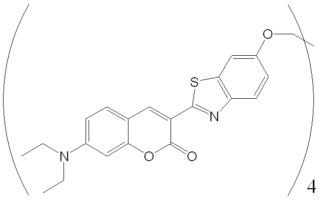
- the first dye oligomer the tetramer oligomer used in Invention Example 3 was used as a dimer (molecular weight 760).
- the concentration of DCM-1 used as the second dye was 12% by weight. Except for the above, a multicolor organic EL device was obtained in the same manner as Example 2 of the present invention.
- Example 3 A multicolor light-emitting organic EL device was obtained in the same manner as Example 3 except that coumarin 6 was not oligomerized. In addition, since it did not oligomerize, since solid content coagulated, the color conversion film could not be formed.
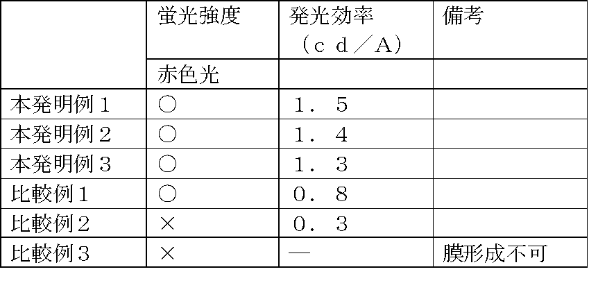
- ⁇ Evaluation items> For each of the organic EL devices of Invention Examples 1 to 3 and Comparative Examples 1 to 3, a light source was disposed on the color conversion film side and irradiated with light having a wavelength of 450 to 490 nm. Furthermore, the light emitted through the color conversion film was measured using a spectral luminance meter (Konica Minolta CS-1000), and the emitted light intensity (fluorescence intensity) of red light having a wavelength of 610 nm was measured. In addition, about fluorescence intensity, the fluorescence quantum efficiency was calculated
- a spectral luminance meter Konica Minolta CS-1000
- each organic EL device of the present invention shows better luminous efficiency than the conventional product using a thick film color conversion film. This is considered to be due to effectively acting on the luminous efficiency.
- Comparative Example 2 since the ratio of the first dye is remarkably small with respect to each of the present invention examples, the incident light absorption function of the first dye is not sufficiently exhibited, and the light emission efficiency is extremely low. Conceivable.
Landscapes
- Physics & Mathematics (AREA)
- Optics & Photonics (AREA)
- Chemical & Material Sciences (AREA)
- General Physics & Mathematics (AREA)
- Engineering & Computer Science (AREA)
- Materials Engineering (AREA)
- Organic Chemistry (AREA)
- Electroluminescent Light Sources (AREA)
Abstract
Description
12 透明支持体
14 ブラックマトリクス
16 赤色カラーフィルター
18 緑色カラーフィルター
20 青色カラーフィルター
22 バンク
24 赤色変換膜
30 有機EL発光部
32 基板
34 TFT素子
36 絶縁膜
38 層間絶縁膜
40 第1電極
42 有機EL膜
44 第2電極
46 無機バリア層
50 シール材
本発明の色変換膜は、青緑色の発光を行う有機EL発光部からの光を吸収して、より長波長の可視光に変換し、2種の色素からなり、第1色素は、色変換膜への入射光を吸収して、そのエネルギーを第2色素へと移動させる色素であり、第2色素は、第1色素から該エネルギーを受容して光を放射する色素であり、第1色素は、平均分子量が1000から1000000の高分子色素である、色変換膜である。
第1色素は、色変換膜への入射光、即ち有機EL素子の発した青緑色の光を吸収し、吸収したエネルギーを第2色素に移動させる色素である。このため、第1色素の吸収スペクトルは有機EL素子の発光スペクトルと重複していることが好ましく、第1色素の吸収極大と有機EL素子の発光スペクトルの極大とが一致していることがより好ましい。例えば、第1色素の光吸収スペクトルの極大波長は、有機EL素子が青緑色の発光を行うことを考慮すれば、400~500nmであることが好ましい。
前述のように、第1色素の発光スペクトルが第2色素の吸収スペクトルと重複していることが好ましく、第1色素の発光スペクトルの極大と第2色素の吸収スペクトルの極大とが一致していることがより好ましい。このため、第2色素が放射する光は、第1色素が吸収する光よりも長波長である。

本発明の色変換膜は、例えば、透明支持体又はカラーフィルター上に第1色素及び第2色素を混合した液体を塗布することによって作製することができる。透明支持体としては、ガラス、ポリイミド、ポリカーボネート、ポリエチレンテレフタレート、ポリエチレンナフタレート、ポリブチレンテレフタレート、ポリエチレンスルホンなどの高分子材料を用いることができる。色変換膜に高分子材料を用いる場合には、透明支持体は剛直であっても可撓性であってもよい。透明支持体は可視光に対して80%以上の透過率を有することが好ましい。
本発明の多色発光有機ELデバイスは、有機EL素子と、上述の色変換膜とを含み、該有機EL素子は、少なくとも一方が透明である一対の電極と、該一対の電極に挟持される有機EL層とを含むデバイスである。
図1に示すように、色変調部10は、同図の上方から順に、透明支持体12に、ブラックマトリクス14、赤色カラーフィルター16、緑色カラーフィルター18、青色カラーフィルター20、バンク22、及び赤色変換膜24が順次形成された積層体である。
まず、図2(a)に示すように、透明支持体12を準備する。透明支持体12としては、ガラス、ポリイミド、ポリカーボネート、ポリエチレンテレフタレート、ポリエチレンナフタレート、ポリブチレンテレフタレート、ポリエチレンスルホンなどの高分子材料を用いることができる。本発明では、上述したとおり、赤色変換膜24に高分子材料を用いる。このため、透明支持体12は剛直であっても可撓性であってもよい。透明支持体12は、可視光に対して80%以上の透過率を有することが好ましい。
次に、図2(b)に示すように、透明支持体12に、ブラックマトリクス14を形成する。ブラックマトリクス14は、後述する各カラーフィルター16~20の配設位置におけるコントラストの向上を目的として配設された層である。ブラックマトリクス14としては、可視域を透過しない材料を使用する。
更に、図2(c)に示すように、透明支持体12上のブラックマトリクス14により画成された領域に、各カラーフィルター16~20を形成する。カラーフィルターとしては、600nm以上の波長を透過する赤色カラーフィルター16、500nm~550nmの波長を透過する緑色カラーフィルター18、及び400nm~550nmの波長を透過する青色カラーフィルター20をそれぞれ配列する。
続いて、図2(d)に示すように、ブラックマトリクス14上に、バンク22を形成する。バンク22の材料としては、レジストなどの光硬化性樹脂又は光熱併用型硬化性樹脂を用いることができる。バンク22はフォトプロセスを用いて形成することが、画素の優れたパターン精度を得る観点で好ましい。
最後に、図2(e)に示すように、カラーフィルター16~20とバンク22とによって画成された領域に、色変換膜24を形成する。色変換膜24の形成方法については、上述したとおりである。なお、図2(e)で示す例は、カラーフィルター上に赤色変換膜を形成した例である。
図1に示すように、有機EL発光部30は、同図の下方から、基板32に、TFT素子34、絶縁膜36、層間絶縁膜38、第1電極40、有機EL膜42、第2電極44、及び無機バリア層46が順次形成された積層体である。
本発明の多色発光有機ELデバイスは、上述の色変調部10側から光を取り出すため、有機EL発光部の基板32は必ずしも透明でなくてよい。例えば、Al等の金属材料、ガラス、石英などの非晶質基板、及び樹脂等の透明ないし半透明材料を用いることができる。或いはまた、Si、GaAsなどの結晶性基板のように不透明な材料を用いることもできる。更に、ガラス等のほか、アルミナ等のセラミックス、ステンレス等の金属シートに表面酸化などの絶縁処理を施した材料、フェノール樹脂等の熱硬化性樹脂、及びポリカーボネート等の熱可塑性樹脂などを用いることもできる。
TFT素子34は、ゲート電極をゲート絶縁膜の下に設けたボトムゲートタイプであって、能動層として多結晶シリコン膜を用いた構造体である。具体的には、従来の多結晶シリコンTFTを用いることができる。
絶縁層36及び層間絶縁膜38は、酸化ケイ素、窒化ケイ素などの無機系材料をスパッタ又は真空蒸着で成膜した層、スピン・オン・グラス(SOG)で形成した酸化ケイ素層、フォトレジスト、ポリイミド、アクリル樹脂などの樹脂系材料の塗膜など、絶縁性を有するものを用いる。絶縁層36及び層間絶縁膜38の接触領域には配線電極等が存在するので、これら36,38をパターニングする際に配線電極等にダメージを与えないようなパターニングが可能な材料を用いることが好ましい。
第1電極(陽極)40は、例えば、メタル電極を配線電極上に形成し、次いで、その上部表面に透明酸化物を形成することで得られる。
有機EL膜42は、正孔注入層、正孔輸送層、有機発光層、電子輸送層、及び電子注入層などの複数の層を積層してなり、基板全面に画素領域を開口した蒸着マスクを用いず、真空蒸着法により各層を順次形成することができる。以下に、例示的な有機EL膜42の構成を、その両側に配置する陽極(第1電極40)及び陰極(第2電極44)とともに示す。
(1)陽極/有機発光層/陰極
(2)陽極/正孔注入層/有機発光層/陰極
(3)陽極/有機発光層/電子注入層/陰極
(4)陽極/正孔注入層/有機発光層/電子注入層/陰極
(5)陽極/正孔注入層/正孔輸送層/有機発光層/電子注入層/陰極
有機EL膜42上に形成する第2電極44は、例えば、蒸着法、スパッタリング法などによりバッファ層を成膜し、その上に透明電極材料である金属酸化物を更に成膜することにより形成することができる。
無機バリア膜46には、SiNx、SiOxNyなどが用いられ、プラズマCVD法等により形成することができる。
上述のように形成された、色変調部10と有機EL発光部30とを、対向して重ねあわせる。具体的には、乾燥窒素雰囲気(酸素及び水分濃度ともに10ppm以下)のグローブボックス内に、色変調部10と有機EL発光部30とを導入する。次いで、図1に示すように、紫外硬化型樹脂からなるシール材50をこれら10,30の各端部間に配置し、多色発光有機ELデバイスを得る。
透明基板として500mm×500mm×0.50mmのコーニングガラスを用意した。このガラス基板上に、スピンコート法によって黒色色素を含むレジスト樹脂を塗布し、フォトリソグラフ法によってパターニングを実施した。これにより、カラーフィルター形成用の開口部を残して膜厚2μmのブラックマトリクスを得た。なお、副画素間は0.100mm幅とし、画素間は0.116mm幅としてパターン形成を行った。
基板として500mm×500mm×0.50mmのガラス基板を用意した。このガラス基板上に、TFT素子を公知の方法により形成した。
続いて、上述のようにして得られた赤色変換層を含む色変調部と、有機EL発光部とを、乾燥窒素雰囲気(酸素及び水分濃度ともに10ppm以下)下に導入し、UV硬化接着剤を用いて以下のように封止した。
本発明例1の赤色変換層の作製において、第1色素はジメチルフェニルで終端したポリ[(9,9-ジオクチル-2,7-ジビニレン-フルオレニル)-Alt-Co-{2-メトキシ-5-(2-エチル-へキロキシ)-1,4-フェニレン}](平均の分子量が50000)、第2色素として4-ジシアノメチレン-2-メチル-6-(p-ジメチルアミノスチリル)-4H-ピラン(DCM-1)を用いた。第1色素及び第2色素の混合物における第2色素の濃度は0.2重量%とした。このような混合物10重量部をトルエン1000重量部に溶解させてインクを調整した。
本発明例1の赤色変換層の作製において、第1色素のオリゴマーとして、ハロゲン化したクマリン6とペンタエリスリトールとをWilliamsonエーテル合成法で調製した、以下の化合物(化A)を用いた。
赤色変換層を、以下に示しように、従来の樹脂分散方式の厚膜で形成した。
本例は、第1色素の分子量が本発明の範囲外、即ち、該分子量が低い例である。第1色素のオリゴマーとして、本発明例3で用いた4量体のオリゴマーを2量体(分子量760)として用いた。第2色素として用いたDCM-1の濃度は、12重量%とした。以上の事項以外は、本発明例2と同様にして多色発光有機ELデバイスを得た。
クマリン6をオリゴマー化しなかったこと以外は、本発明例3と同様にして多色発光有機ELデバイスを得た。なお、オリゴマー化しなかったことから、固形分が凝固したため、色変換膜は形成できなかった。
本発明例1~3及び比較例1~3の各有機ELデバイスについて、色変換膜側に光源を配置して、波長450~490nmの光を照射した。更に、色変換膜を通して出射した光を、分光輝度計(コニカミノルタCS-1000)を用いて測定し、波長610nmの赤色光の出射光強度(蛍光強度)を測定した。なお、蛍光強度については、赤色光について、蛍光量子効率を求め、その値が0.5以上の場合を合格(○)とし、0.5未満の場合は、不合格(×)とした。
Claims (16)
- 青緑色の発光を行う有機EL発光部からの光を吸収して、より長波長の可視光に変換する色変換膜において、
該色変換膜は2種の色素からなり、
第1色素は、色変換膜への入射光を吸収して、そのエネルギーを第2色素へと移動させる色素であり、
第2色素は、第1色素から該エネルギーを受容して光を放射する色素であり、
第1色素は、平均分子量が1000から1000000の高分子色素であることを特徴とする、色変換膜。 - 第2色素は、平均分子量が1000から1000000の高分子色素であることを特徴とする、請求項1に記載の色変換膜。
- 第2色素は、平均分子量が1000未満の低分子色素であることを特徴とする、請求項1に記載の色変換膜。
- 第1色素が、蛍光発光するコア同士が非共有性の連結基で結合されたオリゴマーであることを特徴とする、請求項1~3のいずれかに記載の色変換膜。
- 第1色素の光吸収スペクトルの極大波長が400~500nmであり、その蛍光スペクトルの極大波長が500~550nmであることを特徴とする、請求項4記載の色変換膜。
- 第2色素の光吸収スペクトルの極大波長が500~550nmであり、その蛍光スペクトルの極大波長が550~650nmであることを特徴とする、請求項4に記載の色変換膜。
- 第2色素が、色変換膜の10重量%以下の量で存在することを特徴とする、請求項4に記載の色変換膜。
- 塗布法によって形成されることを特徴とする、請求項4に記載の色変換膜。
- 少なくとも一方が透明電極である一対の電極と、該一対の電極に挟持された有機EL層と、色変換膜とを備える多色発光有機ELデバイスにおいて、
該色変換膜は2種の色素からなり、
第1色素は、色変換膜への入射光を吸収して、そのエネルギーを第2色素へと移動させる色素であり、
第2色素は、第1色素から該エネルギーを受容して光を放射する色素であり、
第1色素は、平均分子量が1000から1000000の高分子色素であることを特徴とする、多色発光有機ELデバイス。 - 第2色素は、平均分子量が1000から1000000の高分子色素であることを特徴とする、請求項9に記載の多色発光有機ELデバイス。
- 第2色素は、平均分子量が1000未満の低分子色素であることを特徴とする、請求項9に記載の多色発光有機ELデバイス。
- 第1色素が、発光コア同士が非共有性の連結基で結合されたオリゴマーであることを特徴とする、請求項9~11のいずれかに記載の多色発光有機ELデバイス。
- 第1色素の光吸収スペクトルの極大波長が400~500nmであり、その蛍光スペクトルの極大波長が500~550nmであることを特徴とする、請求項12に記載の多色発光有機ELデバイス。
- 第2色素の光吸収スペクトルの極大波長が500~550nmであり、その蛍光スペクトルの極大波長が550~650nmであることを特徴とする、請求項12に記載の多色発光有機ELデバイス。
- 第2色素が、色変換膜の10重量%以下の量で存在することを特徴とする、請求項12に記載の多色発光有機ELデバイス。
- 前記色変換膜が塗布法によって形成されていることを特徴とする、請求項12に記載の多色発光有機ELデバイス。
Priority Applications (8)
| Application Number | Priority Date | Filing Date | Title |
|---|---|---|---|
| KR1020107014090A KR101237638B1 (ko) | 2009-01-21 | 2009-01-21 | 색변환막 및 해당 색변환막을 포함하는 다색 발광 유기 el 디바이스 |
| JP2010520087A JP5236732B2 (ja) | 2009-01-21 | 2009-01-21 | 色変換膜及び該色変換膜を含む多色発光有機elデバイス |
| CN200980103551.8A CN101933397A (zh) | 2009-01-21 | 2009-01-21 | 色变换膜和包含该色变换膜的多色发光的有机el设备 |
| KR1020127018142A KR101241627B1 (ko) | 2009-01-21 | 2009-01-21 | 색변환막 및 해당 색변환막을 포함하는 다색 발광 유기 el 디바이스 |
| US12/747,882 US8541777B2 (en) | 2009-01-21 | 2009-01-21 | Color conversion film and multicolor-emitting, organic electroluminescent device comprising the color conversion film |
| PCT/JP2009/050880 WO2010084587A1 (ja) | 2009-01-21 | 2009-01-21 | 色変換膜及び該色変換膜を含む多色発光有機elデバイス |
| TW099101475A TWI494020B (zh) | 2009-01-21 | 2010-01-20 | A color conversion film, and a multi-color light emitting organic EL device containing the color conversion film |
| US14/034,317 US8847219B2 (en) | 2009-01-21 | 2013-09-23 | Color conversion film and multicolor-emitting, organic electroluminescent device comprising the color conversion film |
Applications Claiming Priority (1)
| Application Number | Priority Date | Filing Date | Title |
|---|---|---|---|
| PCT/JP2009/050880 WO2010084587A1 (ja) | 2009-01-21 | 2009-01-21 | 色変換膜及び該色変換膜を含む多色発光有機elデバイス |
Related Child Applications (2)
| Application Number | Title | Priority Date | Filing Date |
|---|---|---|---|
| US12/747,882 A-371-Of-International US8541777B2 (en) | 2009-01-21 | 2009-01-21 | Color conversion film and multicolor-emitting, organic electroluminescent device comprising the color conversion film |
| US14/034,317 Division US8847219B2 (en) | 2009-01-21 | 2013-09-23 | Color conversion film and multicolor-emitting, organic electroluminescent device comprising the color conversion film |
Publications (1)
| Publication Number | Publication Date |
|---|---|
| WO2010084587A1 true WO2010084587A1 (ja) | 2010-07-29 |
Family
ID=42355661
Family Applications (1)
| Application Number | Title | Priority Date | Filing Date |
|---|---|---|---|
| PCT/JP2009/050880 Ceased WO2010084587A1 (ja) | 2009-01-21 | 2009-01-21 | 色変換膜及び該色変換膜を含む多色発光有機elデバイス |
Country Status (6)
| Country | Link |
|---|---|
| US (2) | US8541777B2 (ja) |
| JP (1) | JP5236732B2 (ja) |
| KR (2) | KR101237638B1 (ja) |
| CN (1) | CN101933397A (ja) |
| TW (1) | TWI494020B (ja) |
| WO (1) | WO2010084587A1 (ja) |
Cited By (2)
| Publication number | Priority date | Publication date | Assignee | Title |
|---|---|---|---|---|
| WO2013065649A1 (ja) * | 2011-10-31 | 2013-05-10 | シャープ株式会社 | 有機発光素子 |
| US9099409B2 (en) | 2011-11-18 | 2015-08-04 | Sharp Kabushiki Kaisha | Organic electroluminescent display device, electronic apparatus including the same, and method for producing organic electroluminescent display device |
Families Citing this family (20)
| Publication number | Priority date | Publication date | Assignee | Title |
|---|---|---|---|---|
| JP6019997B2 (ja) | 2012-09-26 | 2016-11-02 | ソニー株式会社 | 表示装置および電子機器 |
| KR102081209B1 (ko) * | 2013-03-26 | 2020-02-26 | 삼성디스플레이 주식회사 | 유기 발광 표시 장치 및 그 제조 방법, 및 그 유기 발광 표시 장치의 제조에 사용되는 도너 기판 및 도너 기판 세트 |
| KR20150033198A (ko) | 2013-09-23 | 2015-04-01 | 삼성디스플레이 주식회사 | 양자점 발광 소자 및 표시 장치 |
| US10903330B2 (en) * | 2013-11-27 | 2021-01-26 | General Electric Company | Tapered gate electrode for semiconductor devices |
| KR102255809B1 (ko) * | 2013-12-02 | 2021-05-24 | 엘지디스플레이 주식회사 | 유기 발광 표시장치 |
| DE102013113533A1 (de) * | 2013-12-05 | 2015-06-11 | Osram Oled Gmbh | Konversionselement und Verfahren zur Herstellung eines Konversionselements |
| CN103700687A (zh) * | 2013-12-20 | 2014-04-02 | 京东方科技集团股份有限公司 | 有机电致发光显示面板及其制造方法、显示装置 |
| KR102168045B1 (ko) * | 2013-12-30 | 2020-10-20 | 엘지디스플레이 주식회사 | 유기 발광 표시장치 |
| KR20150106029A (ko) | 2014-03-10 | 2015-09-21 | 삼성디스플레이 주식회사 | 백라이트 어셈블리 및 이를 포함하는 표시 장치 |
| CN104076564A (zh) * | 2014-06-09 | 2014-10-01 | 京东方科技集团股份有限公司 | 阵列基板及其制备方法、显示装置 |
| KR102362620B1 (ko) | 2014-12-09 | 2022-02-14 | 삼성디스플레이 주식회사 | 유기발광 표시장치 및 그의 제조방법 |
| KR20160076406A (ko) * | 2014-12-22 | 2016-06-30 | 삼성디스플레이 주식회사 | 디스플레이 장치, 색변환 필름 및 그들의 제조방법 |
| KR102386848B1 (ko) * | 2015-04-13 | 2022-04-15 | 삼성디스플레이 주식회사 | 표시장치 및 그 제조방법 |
| KR102369633B1 (ko) * | 2015-08-31 | 2022-03-03 | 엘지디스플레이 주식회사 | 유기발광다이오드표시장치 및 이의 제조방법 |
| KR102784236B1 (ko) * | 2016-09-28 | 2025-03-21 | 삼성전자주식회사 | 디스플레이 장치 |
| NL2018826B1 (en) * | 2017-05-02 | 2018-11-09 | Spgprints B V | One-pot synthesis of reactive deep black |
| KR102887309B1 (ko) * | 2019-03-18 | 2025-11-18 | 삼성디스플레이 주식회사 | 표시패널 및 이의 제조 방법 |
| CN110911459B (zh) * | 2019-11-13 | 2022-05-13 | 清华大学 | 一种色转换有机电致发光装置 |
| KR102872426B1 (ko) * | 2020-08-27 | 2025-10-17 | 엘지전자 주식회사 | 반도체 발광 소자를 이용한 디스플레이 장치 |
| KR20220094271A (ko) * | 2020-12-28 | 2022-07-06 | 삼성디스플레이 주식회사 | 색변환 기판, 표시 장치 및 색변환 기판의 제조 방법 |
Citations (5)
| Publication number | Priority date | Publication date | Assignee | Title |
|---|---|---|---|---|
| WO2000018193A1 (en) * | 1998-09-17 | 2000-03-30 | Seiko Epson Corporation | Method for manufacturing electroluminescence device |
| JP2000273316A (ja) * | 1999-03-26 | 2000-10-03 | Idemitsu Kosan Co Ltd | 蛍光媒体、蛍光媒体の製造方法および蛍光媒体を用いた有機エレクトロルミネッセンス表示装置 |
| WO2006103907A1 (ja) * | 2005-03-29 | 2006-10-05 | Idemitsu Kosan Co., Ltd. | 赤色蛍光変換媒体及びそれを用いた色変換基板、発光デバイス |
| JP2007157550A (ja) * | 2005-12-06 | 2007-06-21 | Fuji Electric Holdings Co Ltd | 色変換膜およびそれを用いた多色発光有機elデバイス |
| JP2008056797A (ja) * | 2006-08-31 | 2008-03-13 | Tokyo Institute Of Technology | 蛍光材料、及びそれを用いた光デバイス |
Family Cites Families (5)
| Publication number | Priority date | Publication date | Assignee | Title |
|---|---|---|---|---|
| JPH10338872A (ja) * | 1997-06-09 | 1998-12-22 | Tdk Corp | 色変換材料およびこれを用いた有機elカラーディスプレイ |
| JP2000026852A (ja) | 1998-07-09 | 2000-01-25 | Idemitsu Kosan Co Ltd | 色変換膜および発光装置 |
| WO2006061954A1 (ja) * | 2004-12-08 | 2006-06-15 | Fuji Electric Holdings Co., Ltd. | 有機el素子 |
| KR101308203B1 (ko) * | 2005-12-14 | 2013-09-13 | 샤프 가부시키가이샤 | 유기 el 디스플레이의 제조 방법 |
| CN101743782A (zh) * | 2007-09-19 | 2010-06-16 | 富士电机控股株式会社 | 色变换滤光片、以及色变换滤光片和有机el显示器的制造方法 |
-
2009
- 2009-01-21 WO PCT/JP2009/050880 patent/WO2010084587A1/ja not_active Ceased
- 2009-01-21 KR KR1020107014090A patent/KR101237638B1/ko not_active Expired - Fee Related
- 2009-01-21 KR KR1020127018142A patent/KR101241627B1/ko not_active Expired - Fee Related
- 2009-01-21 US US12/747,882 patent/US8541777B2/en not_active Expired - Fee Related
- 2009-01-21 JP JP2010520087A patent/JP5236732B2/ja not_active Expired - Fee Related
- 2009-01-21 CN CN200980103551.8A patent/CN101933397A/zh active Pending
-
2010
- 2010-01-20 TW TW099101475A patent/TWI494020B/zh not_active IP Right Cessation
-
2013
- 2013-09-23 US US14/034,317 patent/US8847219B2/en not_active Expired - Fee Related
Patent Citations (5)
| Publication number | Priority date | Publication date | Assignee | Title |
|---|---|---|---|---|
| WO2000018193A1 (en) * | 1998-09-17 | 2000-03-30 | Seiko Epson Corporation | Method for manufacturing electroluminescence device |
| JP2000273316A (ja) * | 1999-03-26 | 2000-10-03 | Idemitsu Kosan Co Ltd | 蛍光媒体、蛍光媒体の製造方法および蛍光媒体を用いた有機エレクトロルミネッセンス表示装置 |
| WO2006103907A1 (ja) * | 2005-03-29 | 2006-10-05 | Idemitsu Kosan Co., Ltd. | 赤色蛍光変換媒体及びそれを用いた色変換基板、発光デバイス |
| JP2007157550A (ja) * | 2005-12-06 | 2007-06-21 | Fuji Electric Holdings Co Ltd | 色変換膜およびそれを用いた多色発光有機elデバイス |
| JP2008056797A (ja) * | 2006-08-31 | 2008-03-13 | Tokyo Institute Of Technology | 蛍光材料、及びそれを用いた光デバイス |
Cited By (2)
| Publication number | Priority date | Publication date | Assignee | Title |
|---|---|---|---|---|
| WO2013065649A1 (ja) * | 2011-10-31 | 2013-05-10 | シャープ株式会社 | 有機発光素子 |
| US9099409B2 (en) | 2011-11-18 | 2015-08-04 | Sharp Kabushiki Kaisha | Organic electroluminescent display device, electronic apparatus including the same, and method for producing organic electroluminescent display device |
Also Published As
| Publication number | Publication date |
|---|---|
| US8847219B2 (en) | 2014-09-30 |
| TW201039684A (en) | 2010-11-01 |
| US20120032151A1 (en) | 2012-02-09 |
| US8541777B2 (en) | 2013-09-24 |
| JP5236732B2 (ja) | 2013-07-17 |
| KR101241627B1 (ko) | 2013-03-11 |
| JPWO2010084587A1 (ja) | 2012-07-12 |
| KR20100108535A (ko) | 2010-10-07 |
| US20140014941A1 (en) | 2014-01-16 |
| KR101237638B1 (ko) | 2013-02-27 |
| KR20120098880A (ko) | 2012-09-05 |
| CN101933397A (zh) | 2010-12-29 |
| TWI494020B (zh) | 2015-07-21 |
Similar Documents
| Publication | Publication Date | Title |
|---|---|---|
| JP5236732B2 (ja) | 色変換膜及び該色変換膜を含む多色発光有機elデバイス | |
| WO2003079735A1 (fr) | Dispositif d'emission de couleur | |
| JP2016122606A (ja) | 波長変換方式発光装置並びにこれを備えた表示装置、照明装置および電子機器 | |
| WO2004036960A1 (ja) | 有機エレクトロルミネッセンス表示装置及びその製造方法 | |
| WO2016204166A1 (ja) | 波長変換方式発光装置並びにこれを備えた表示装置、照明装置および電子機器 | |
| JP2004335207A (ja) | 有機el素子とその製造方法 | |
| CN101305643B (zh) | 有机el发光显示器 | |
| JP2007115419A (ja) | 有機発光素子 | |
| JP3591728B2 (ja) | 有機elディスプレイ | |
| US20070109571A1 (en) | Color filter with color conversion function, producing method thereof, and organic el display | |
| WO2010106619A1 (ja) | 色変換フィルター基板 | |
| JP5450738B2 (ja) | 色変換膜及び該色変換膜を含む有機elデバイス | |
| WO2010092694A1 (ja) | 色変換基板およびそれを用いた有機elディスプレイ | |
| JPWO2006028089A1 (ja) | 発光デバイスおよびその製造方法 | |
| JP2010146760A (ja) | 色変換フィルタパネル、パネル型有機el発光部およびカラー有機elディスプレイ | |
| JP2004103519A (ja) | 色変換カラーフィルタ基板およびこれを用いた有機カラーディスプレイ | |
| JP2009129586A (ja) | 有機el素子 | |
| JP2009205929A (ja) | フルカラー有機elディスプレイパネル | |
| JP2009288476A (ja) | 色変換基板の製造方法、色変換フィルタ基板の製造方法及び有機電界発光素子の製造方法 | |
| JP2008305730A (ja) | 多色発光デバイスの製造方法 | |
| JP3861821B2 (ja) | 有機elディスプレイパネルおよびその製造方法 | |
| JP4618562B2 (ja) | 有機elディスプレイの製造方法 | |
| JP2008077943A (ja) | 多色発光デバイス | |
| JP4552187B2 (ja) | 多色発光デバイスおよびその製造方法 | |
| JP2009087908A (ja) | 有機el素子 |
Legal Events
| Date | Code | Title | Description |
|---|---|---|---|
| WWE | Wipo information: entry into national phase |
Ref document number: 200980103551.8 Country of ref document: CN |
|
| WWE | Wipo information: entry into national phase |
Ref document number: 2010520087 Country of ref document: JP |
|
| ENP | Entry into the national phase |
Ref document number: 20107014090 Country of ref document: KR Kind code of ref document: A |
|
| 121 | Ep: the epo has been informed by wipo that ep was designated in this application |
Ref document number: 09838778 Country of ref document: EP Kind code of ref document: A1 |
|
| NENP | Non-entry into the national phase |
Ref country code: DE |
|
| WWE | Wipo information: entry into national phase |
Ref document number: 12747882 Country of ref document: US |
|
| 122 | Ep: pct application non-entry in european phase |
Ref document number: 09838778 Country of ref document: EP Kind code of ref document: A1 |