WO2010073775A1 - 表示装置および表示装置の駆動方法 - Google Patents
表示装置および表示装置の駆動方法 Download PDFInfo
- Publication number
- WO2010073775A1 WO2010073775A1 PCT/JP2009/064786 JP2009064786W WO2010073775A1 WO 2010073775 A1 WO2010073775 A1 WO 2010073775A1 JP 2009064786 W JP2009064786 W JP 2009064786W WO 2010073775 A1 WO2010073775 A1 WO 2010073775A1
- Authority
- WO
- WIPO (PCT)
- Prior art keywords
- gradation
- data
- correction
- gradation data
- data signal
- Prior art date
- Legal status (The legal status is an assumption and is not a legal conclusion. Google has not performed a legal analysis and makes no representation as to the accuracy of the status listed.)
- Ceased
Links
Images


Classifications
-
- G—PHYSICS
- G09—EDUCATION; CRYPTOGRAPHY; DISPLAY; ADVERTISING; SEALS
- G09G—ARRANGEMENTS OR CIRCUITS FOR CONTROL OF INDICATING DEVICES USING STATIC MEANS TO PRESENT VARIABLE INFORMATION
- G09G3/00—Control arrangements or circuits, of interest only in connection with visual indicators other than cathode-ray tubes
- G09G3/20—Control arrangements or circuits, of interest only in connection with visual indicators other than cathode-ray tubes for presentation of an assembly of a number of characters, e.g. a page, by composing the assembly by combination of individual elements arranged in a matrix no fixed position being assigned to or needed to be assigned to the individual characters or partial characters
- G09G3/34—Control arrangements or circuits, of interest only in connection with visual indicators other than cathode-ray tubes for presentation of an assembly of a number of characters, e.g. a page, by composing the assembly by combination of individual elements arranged in a matrix no fixed position being assigned to or needed to be assigned to the individual characters or partial characters by control of light from an independent source
- G09G3/36—Control arrangements or circuits, of interest only in connection with visual indicators other than cathode-ray tubes for presentation of an assembly of a number of characters, e.g. a page, by composing the assembly by combination of individual elements arranged in a matrix no fixed position being assigned to or needed to be assigned to the individual characters or partial characters by control of light from an independent source using liquid crystals
- G09G3/3611—Control of matrices with row and column drivers
- G09G3/3648—Control of matrices with row and column drivers using an active matrix
-
- H—ELECTRICITY
- H04—ELECTRIC COMMUNICATION TECHNIQUE
- H04N—PICTORIAL COMMUNICATION, e.g. TELEVISION
- H04N9/00—Details of colour television systems
- H04N9/64—Circuits for processing colour signals
- H04N9/68—Circuits for processing colour signals for controlling the amplitude of colour signals, e.g. automatic chroma control circuits
- H04N9/69—Circuits for processing colour signals for controlling the amplitude of colour signals, e.g. automatic chroma control circuits for modifying the colour signals by gamma correction
-
- G—PHYSICS
- G09—EDUCATION; CRYPTOGRAPHY; DISPLAY; ADVERTISING; SEALS
- G09G—ARRANGEMENTS OR CIRCUITS FOR CONTROL OF INDICATING DEVICES USING STATIC MEANS TO PRESENT VARIABLE INFORMATION
- G09G2320/00—Control of display operating conditions
- G09G2320/02—Improving the quality of display appearance
- G09G2320/0233—Improving the luminance or brightness uniformity across the screen
-
- G—PHYSICS
- G09—EDUCATION; CRYPTOGRAPHY; DISPLAY; ADVERTISING; SEALS
- G09G—ARRANGEMENTS OR CIRCUITS FOR CONTROL OF INDICATING DEVICES USING STATIC MEANS TO PRESENT VARIABLE INFORMATION
- G09G2320/00—Control of display operating conditions
- G09G2320/02—Improving the quality of display appearance
- G09G2320/0271—Adjustment of the gradation levels within the range of the gradation scale, e.g. by redistribution or clipping
Definitions
- the present invention relates to a technique for improving the in-plane distribution of display quality in a display panel.
- Non-Patent Document 1 It is generally well known that a feed-through phenomenon occurs in an active matrix type liquid crystal display device using a TFT as a picture element selection element (see, for example, Non-Patent Document 1). Hereinafter, the pull-in phenomenon will be briefly described.
- FIG. 8 shows an equivalent circuit of one picture element.
- One picture element PIX is provided corresponding to the intersection of the gate bus line GL and the source bus line SL.
- the pixel PIX usually includes a parasitic capacitor such as a capacitor Cgd formed between the pixel electrode 102 and the gate bus line GL. Yes.
- the gate of the TFT 101 is connected to the gate bus line GL
- the source of the TFT 101 is connected to the source bus line SL
- the drain of the TFT 101 is connected to the pixel electrode 102.
- the liquid crystal capacitor Clc is formed by disposing a liquid crystal layer between the pixel electrode 102 and the counter electrode to which the voltage Vcom is applied, and the auxiliary capacitor Cs is connected to the pixel electrode 102 or an electrode connected to the pixel electrode 102.
- An insulating film is disposed between the auxiliary capacitor bus line to which the voltage Vcs is applied.
- the voltage Vcs is equal to the voltage Vcom, for example, but may be other values.
- a selection signal Vg composed of binary levels of a gate high potential Vgh and a gate low potential Vgl is output from the gate driver to the gate bus line GL.
- a positive data signal Vsp and a negative data signal Vsn are output from the source driver to the source bus line SL while being switched by AC driving.
- the potential of the pixel electrode 102 is lowered by the voltage ⁇ Vd due to a pull-in phenomenon via the capacitance Cgd which is a parasitic capacitance between the gate bus line GL and the potential of the pixel electrode 102 than the potential of the data signal Vsp Is also low Vdp.
- This voltage ⁇ Vd is called a feed through voltage.
- Cpix Clc + Cs + Cgd.
- the pixel electrode 102 to which the potential Vdp has been written before is turned to the potential Vsn of the data signal Vsn. Will be written.
- the liquid crystal capacitor Clc and the auxiliary capacitor Cs are charged.
- the potential of the pixel electrode 102 decreases by the voltage ⁇ Vd due to the pulling phenomenon through the capacitor Cgd, and the potential of the pixel electrode 102 is lower than the potential of the data signal Vsn. Vdn.
- the gate pulse output from the gate driver to the gate bus line GL is transmitted to each pixel element with a propagation delay.
- the gate of the PIX TFT 101 is reached.
- the gate pulse has a waveform with a larger delay at points farther from the output of the gate driver. For example, as shown in FIG. 10, if the waveform of the gate pulse VG (j) of the gate bus line GL in the jth row generated by the gate driver is an ideal square wave, the picture in the jth row and the first column is shown.
- the delay of the gate pulse Vg (1, j) reaching the element PIX is small, and the delay of the gate pulse Vg (N, j) reaching the pixel PIX in the j-th row and the N-th column is large.
- Formula (1) that can be derived by an electrostatic solution using only the charge conservation law Unlike FIG. 10, as the amount of change SyN of the fall of the gate pulse per unit time shown in FIG. 10 decreases, the transition time until the TFT 101 shifts to the OFF state becomes longer, and the gate pulse after the OFF state is reached. ⁇ Vd becomes smaller as the waveform until the voltage drops to the gate low potential becomes gentle and the feedthrough of the capacitor Cgd becomes smaller.
- the voltage ⁇ Vd has such a distribution that the pixel PIX having a larger distance from the gate driver output on the display panel is smaller. It will be.
- the potential fluctuation of the pixel electrode 102 occurs steeply, causing a potential drop of ⁇ Vd (1), and a gate with a large delay. It is shown that in the pixel PIX to which the pulse Vg (N, j) is applied, the potential fluctuation of the pixel electrode 102 occurs slowly and the potential decreases by ⁇ Vd (N).
- the correction amount of the gradation data has a distribution in the panel surface.
- the positions on the display panel can be expressed using the column positions.
- the voltage ⁇ Vd is larger as the picture element PIX is closer to, and the voltage ⁇ Vd is smaller as the picture element PIX is closer to the column in the panel center C.
- the positive data signal Vsp or the negative data signal Vsn corresponding to a certain gradation data is uniform within the panel surface (that is, the panel horizontal direction) as shown by the broken line.
- the pixel electrode potential Vdp having the positive polarity and the pixel electrode potential Vdn having the negative polarity are indicated by solid lines due to the distribution of the voltage ⁇ Vd. Then, a curved distribution that is convex upward in the column at the center C of the panel is formed.
- the liquid crystal applied voltage based on the positive polarity gradation data becomes the largest at the panel central portion C and gradually decreases from the panel central portion C through the panel intermediate portion B to the both end portions A of the panel.
- the liquid crystal applied voltage based on the tone data is the smallest at the panel center C, and gradually increases from the panel center C through the panel middle B to the panel ends A.
- the gradation data of each picture element is compensated in advance for the distribution of the voltage ⁇ Vd before being supplied to the display driver, that is, close to both ends A of the panel.
- the distribution is corrected so that the data signal potentials Vdp and Vdn become higher.
- the pixel electrode potential Vdp ⁇ Vdn after the pull-in phenomenon occurs becomes uniform within the panel surface as shown by the solid line.
- the gradation data supplied to PIX is corrected so as to increase by a small number of gradations, and corrected so that the number of gradations increases as it goes from the panel center C toward both ends A of the panel.
- the gradation data supplied to the picture element PIX in the panel center C is corrected so as to decrease by a small number of gradations, and the number of gradations is increased so as to decrease from the panel center C toward both ends A of the panel.
- the gradation data is corrected so as to compensate for the in-plane distribution of the voltage ⁇ Vd
- writing to the picture element PIX is performed by the data signal corresponding to the corrected gradation data, and thus the pixel electrode 102 is used.
- the effective values of the positive polarity data signal and the negative polarity data signal can be made equal in the plane uniformly without changing the common electrode potential Vcom. it can.
- FIG. 13 shows the compensation of the voltage ⁇ Vd in consideration of the in-plane distribution for the grayscale data supplied to the source driver for the input grayscale data that exists for 256 grayscales having a total grayscale width of “0” to “255”.
- the sign “VH” is added before the numbers “0” to “255” representing the gradation, and the gradation is assigned to the potential corresponding to the negative polarity gradation data.
- a sign of VL is added in front of the numbers “0” to “255”. This is a common matter throughout this specification.
- the correction is made to increase the tone by the tone bp1 at the panel intermediate portion B and by the tone cp1 at the panel center C.
- the panel intermediate portion B is more than the input end portion A of the panel.
- the gradation data at both ends A of the panel is set to “255” while maintaining the gradation at the same bp2 as the tone difference and at the center C of the panel lower than the both ends A by the same cp2 as the input gradation difference. To correct. In this case, after the pull-in phenomenon occurs, the pixel electrode potentials corresponding to the highest gradation data are uniformly set to VH255 'in the plane.
- the correction is performed so as to decrease by the gradation bn1 at the middle part of the panel and by the gradation cn1 at the panel center C.
- the panel intermediate portion B is set to the input floor higher than the panel end portions A.
- the gradation data at both ends A of the panel is set to “0” while the panel center C is maintained at a gradation lower than the both ends A by the same cn2 as the input gradation difference. To correct. In this case, the pixel electrode potentials corresponding to the highest gradation data are evenly aligned with VL0 'in the plane after the pull-in phenomenon occurs.
- the common electrode potential Vcom is set to a potential that equally divides between the potential VH0 and the potential VL0 '.
- the output gradation width that can be displayed by the pixel PIX after the occurrence of the pull-in phenomenon is the gradation width Rvp corresponding to the difference voltage between the potential VH255 ′ and the potential VH0 for the positive gradation data.
- the negative gradation data has a gradation width Rvn corresponding to the voltage difference between the potential VL0 ′ and the potential VL255. Note that the gradient of the gradation in each of the gradation width Rvp and the gradation width Rvn is arbitrarily designed.
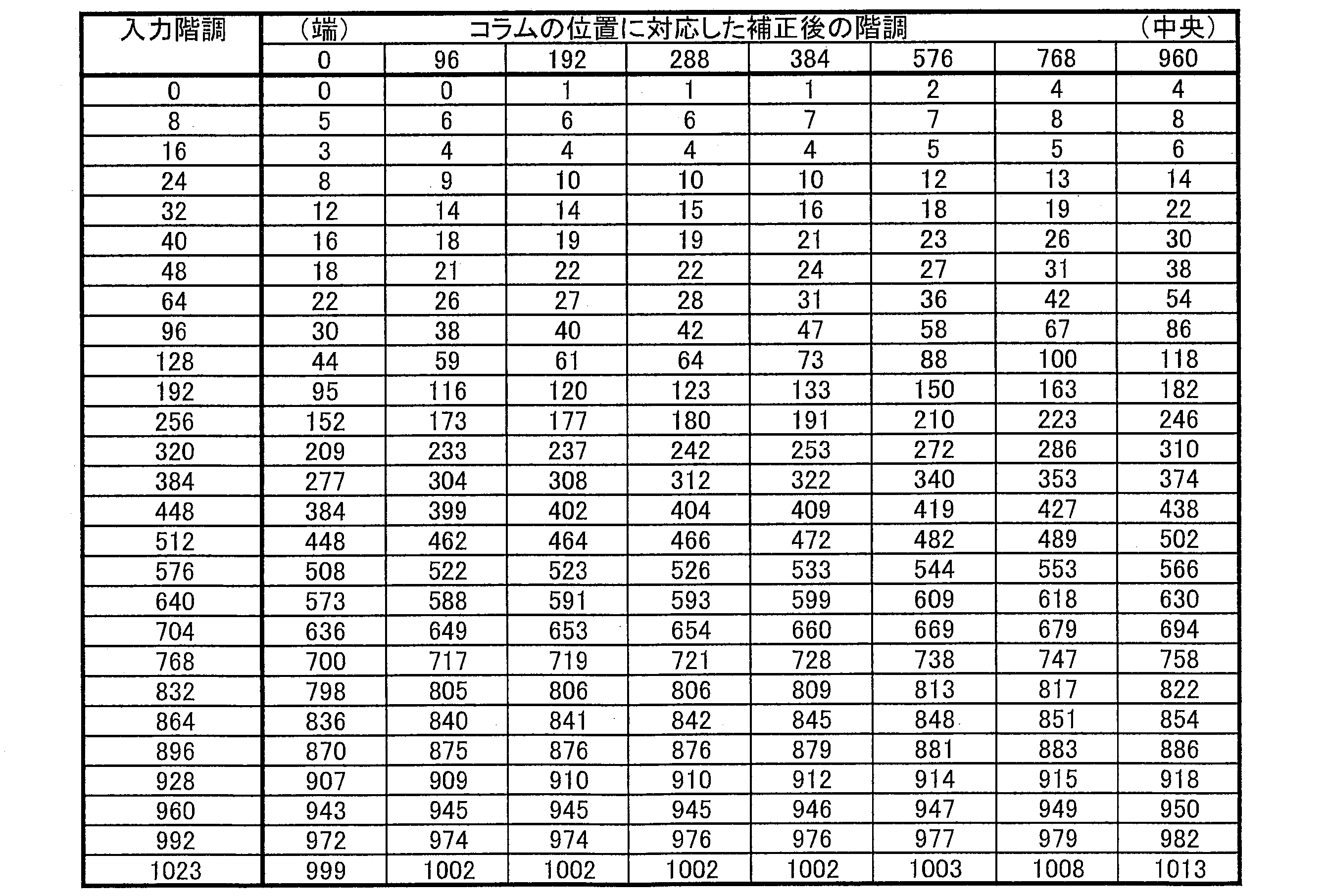
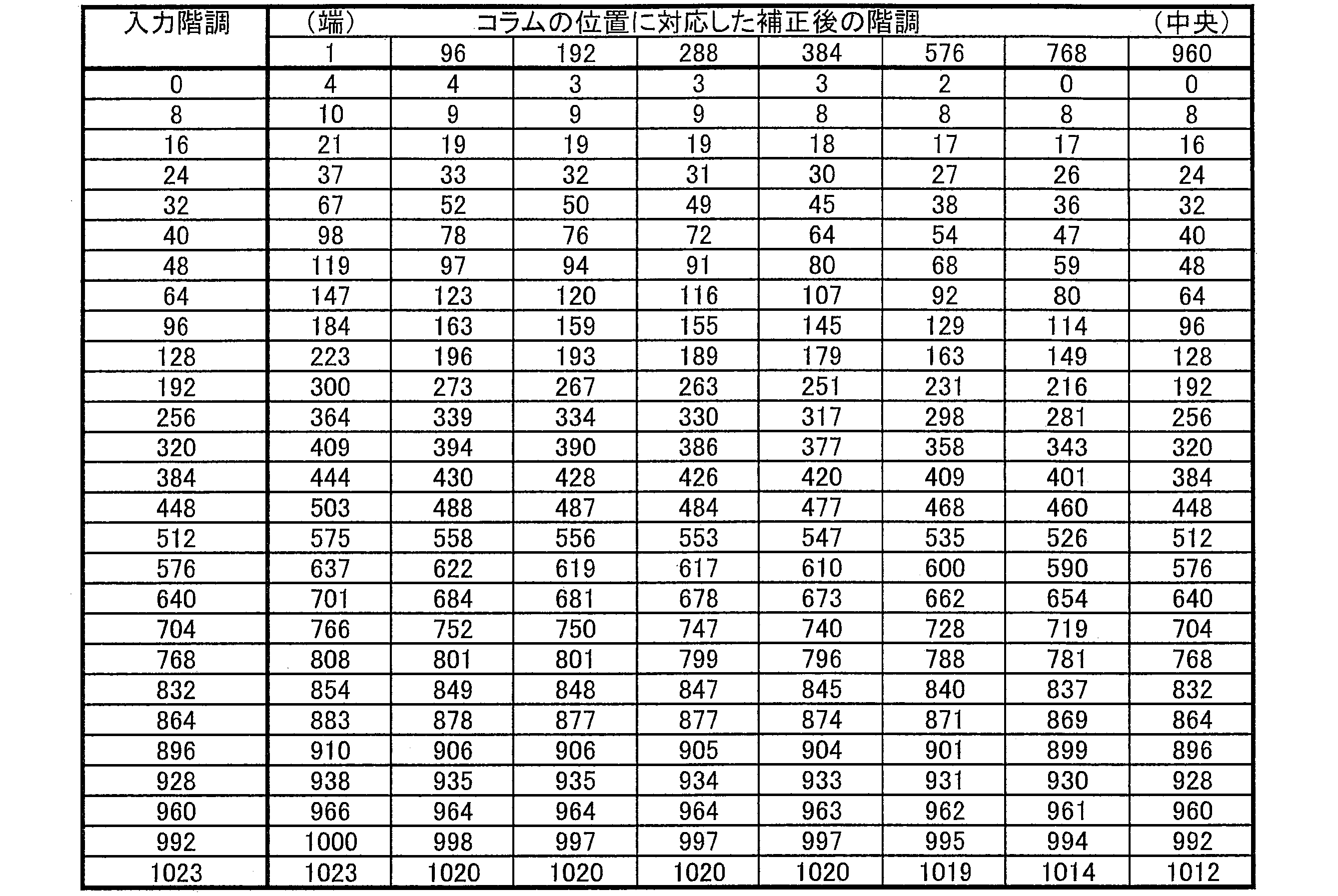
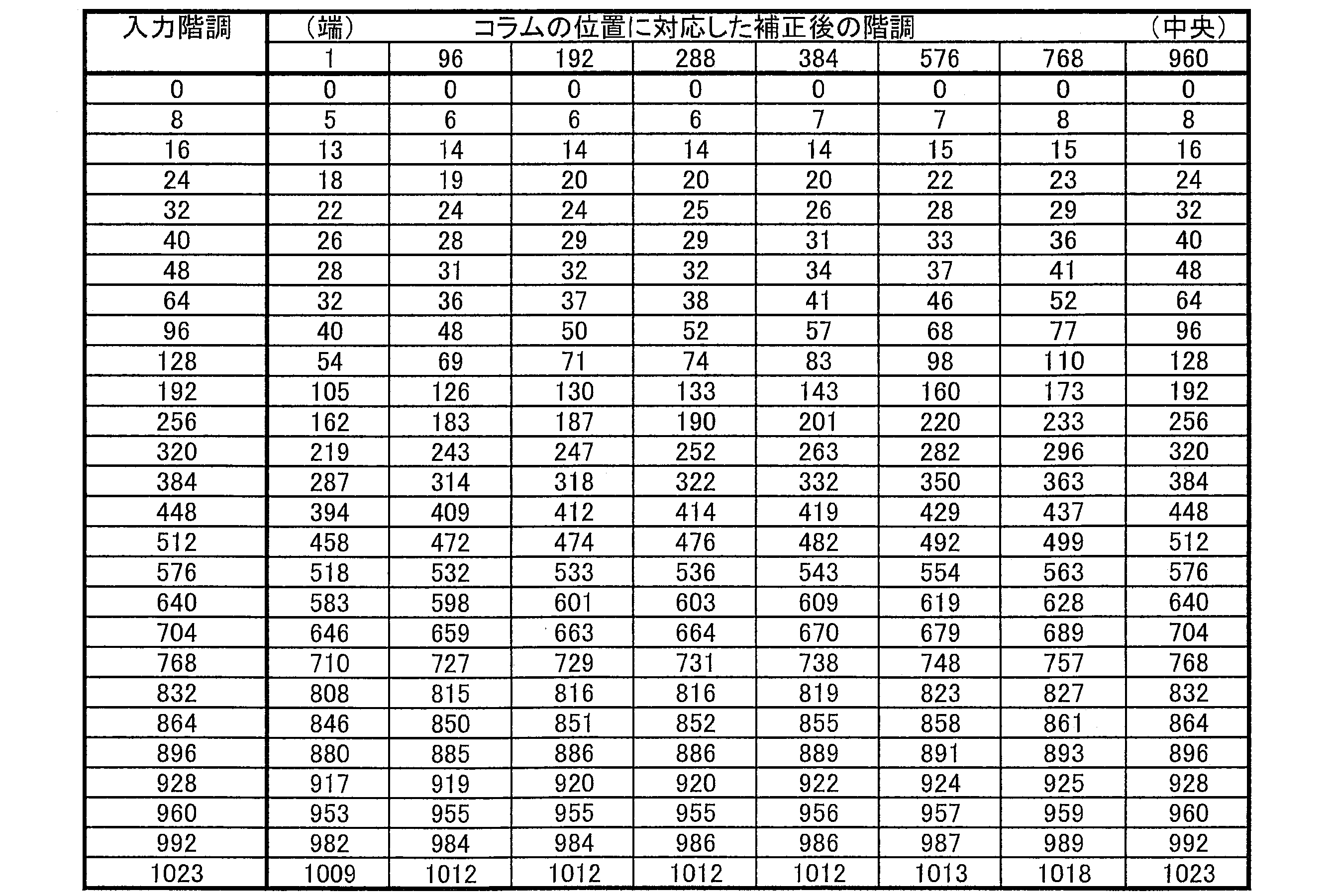
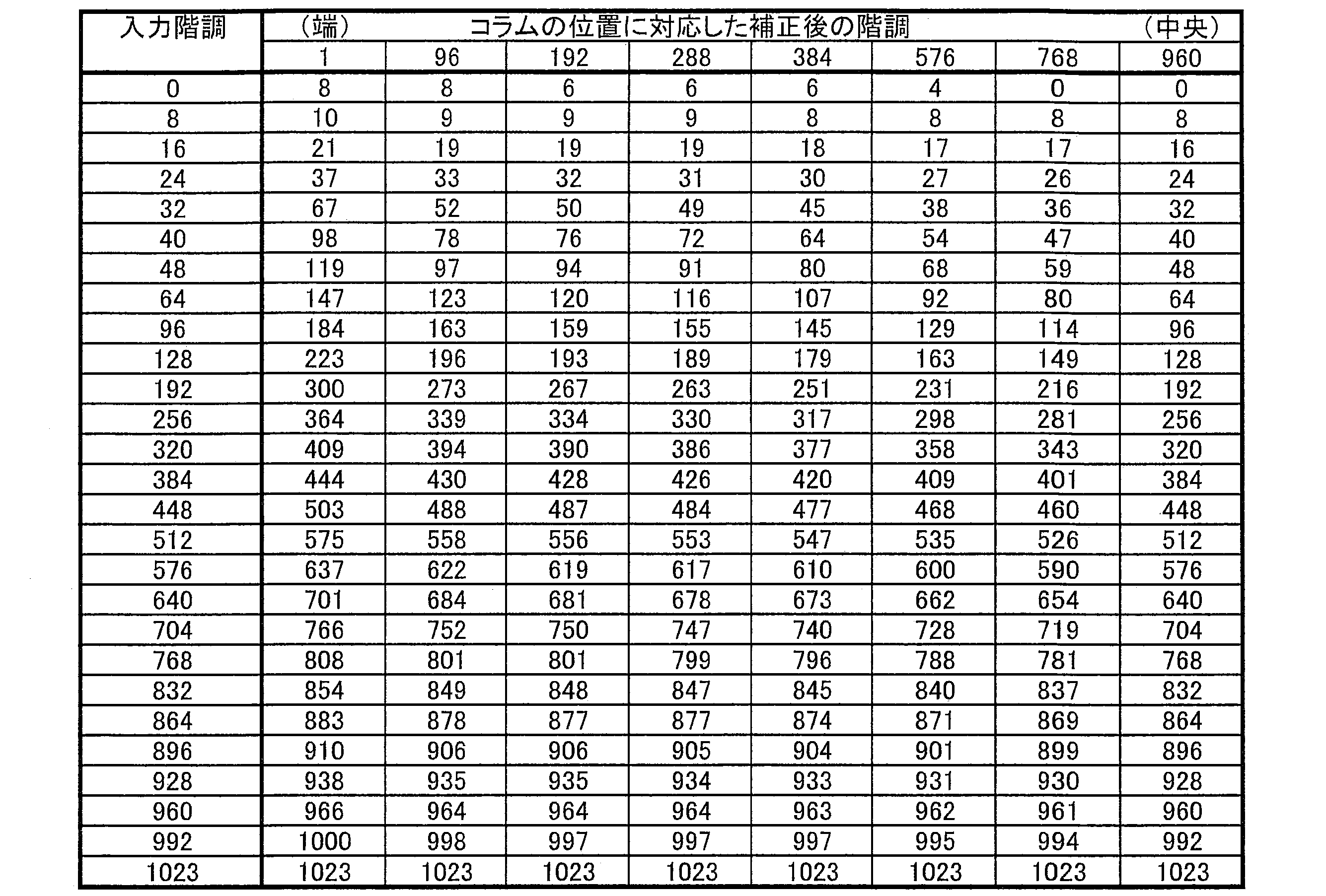
- the relationship between the input gradation data and the corrected gradation data provided in the display controller is stored. This will be described using the look-up table.
- a look-up table for positive tone data is shown in Table 1
- a look-up table for negative tone data is shown in Table 2.
- 256 gradations represented by 8 bits in the above example are converted into 1024 gradations represented by 10 bits, but the purpose is that of 256 gradations. It is the same.
- the display panel is set to full high-definition specifications (1920 ⁇ 1080), that is, the number of columns is set to 1920 for each color of RGB, and the input gradation data and the gradation are set for the position range of columns 0 to 960 corresponding to a half of the display area. The relationship with the tone data after tone correction is shown.
- the lowest positive gradation is obtained even in the panel center portion C having the smallest voltage ⁇ Vd out of the entire gradation width of the input gradation data.
- the gradation cp1 used for the correction amount cannot be used for display.
- the gradation cp2 can not be used for display by maintaining the gradation difference between the two ends A of the panel in the vicinity of the highest polarity data of the positive polarity, and the difference between the two ends A of the panel in the vicinity of the lowest gradation data of the negative polarity. By maintaining the gradation difference, the gradation cn2 cannot be used for display. This narrows the reproduction range as a whole.
- the positive polarity maximum gradation data is corrected to the maximum gradation data (eg, “255”) of the input gradation data, or the negative polarity minimum gradation data is corrected to the input gradation data. Even if it is allowed to correct to the lowest gradation data (for example, “0”), the correction is so as to exceed the maximum gradation data of the input gradation data and below the minimum gradation data of the input gradation data. Since addition and subtraction of quantities cannot be performed, the reproduction range as a whole becomes narrow as a whole.
- the above-described problem with respect to the positive gradation data exists as an inverse relationship between the lowest gradation side and the highest gradation side. Further, the closer to the both ends A of the panel, the larger gradation correction is performed than in the panel center C, and therefore the reproduction range is further narrowed for the same reason.
- bit drop occurs in which some of the bits representing the gradation data cannot be displayed, and the display quality is greatly impaired.
- the present invention has been made in view of the above-described conventional problems, and its purpose is to compensate for a phenomenon in which an in-plane distribution occurs in a pixel electrode potential such as a pull-in phenomenon by correcting gradation data.
- the object is to realize a display device capable of ensuring a wide reproduction range and a driving method of the display device.
- the display device of the present invention is an active matrix type display device that supplies data signals on a display panel to gradation data before being converted into data signals.
- a correction unit that performs gradation correction with a correction amount corresponding to the column position is provided, and the correction unit supplies the input gradation data to at least one column that forms part of all the columns.
- the correction amount is set to zero. It is characterized by gradation correction.
- the correction unit is configured to set the correction amount to zero for the positive minimum gradation data and the negative minimum gradation data for the position of at least one column forming a part of all columns. Tone correction is performed, that is, gradation data equal to the input gradation data is output. As a result, not only the position of at least one column but also the gradation width that can be used for display can be increased over the entire panel including the positions of other columns.
- the correction unit supplies the first gradation data to be supplied to one or more columns located at the center of all the columns of the input gradation data.
- the gradation data at least the gradation data corresponding to the data signal potential having the lowest positive polarity and the gradation data corresponding to the data signal potential having the lowest negative polarity, the gradation correction is performed with the correction amount set to zero. It is characterized by performing.
- the correction unit corrects the positive polarity minimum gradation data and the negative polarity minimum gradation data for the position of one or more columns located in the center of all the columns.
- Gradation correction is performed with the amount set to zero, that is, gradation data equal to the input gradation data is output.
- a display device capable of ensuring a wide reproduction range, especially in the center of the panel, while compensating for the phenomenon of in-plane distribution in the pixel electrode potential, such as the pull-in phenomenon, by correcting the gradation data. There is an effect that can be done.
- the display device of the present invention uses the data signal potential having the highest positive polarity corresponding to the first gradation data after the gradation correction as the first data after the gradation correction.
- the data signal potential having the highest negative polarity corresponding to the first gradation data after the gradation correction is lower than the data signal potential having the highest positive polarity corresponding to the gradation data other than the gradation data. Further, the data signal potential is lower than the data signal potential having the highest negative polarity corresponding to the gradation data other than the first gradation data after the gradation correction.
- the same gradation data supplied to the correction unit is supplied to the pixel electrode as the same data signal potential on the entire surface of the panel, and the same positive polarity gradation data and negative polarity gradation are supplied. Since the effective value of the voltage applied to the display element such as a liquid crystal display element becomes equal to the tone data, there is an effect that uniform display quality can be provided on the entire panel surface.
- the display device of the present invention performs the above-described gradation correction by setting the correction amount to zero for the gradation data corresponding to the data signal potential having the highest positive polarity for all columns.
- the gradation correction corresponding to the data signal potential having the highest negative polarity is characterized by performing the gradation correction with the correction amount set to zero.
- the entire gradation width can be used for display at a certain column position, there is an effect that high display quality can be provided.
- the display device of the present invention performs the above-described gradation correction by setting the correction amount to zero for the gradation data corresponding to the data signal potential having the highest positive polarity for all columns.
- the data signal potential having the highest negative polarity corresponding to the first gradation data after the gradation correction corresponds to the gradation data other than the first gradation data after the gradation correction. It is characterized by being higher than the data signal potential having the highest negative polarity.
- the entire gradation width can be used for display at a certain column position, there is an effect that high display quality can be provided. Further, at each column position, the difference between the pixel electrode potential corresponding to the corrected positive polarity gradation data and the common electrode potential, and the pixel electrode potential corresponding to the corrected negative polarity gradation data, Since the difference from the common electrode potential can be made equal to each other, it is possible to provide high display quality.
- the display device of the present invention is an active matrix type display device that supplies data signals on a display panel to gradation data before being converted into data signals.
- a correction unit that performs gradation correction with a correction amount corresponding to the column position is provided, and the correction unit corresponds to the data signal potential having the lowest positive polarity in all columns of the input gradation data.
- the gradation correction is performed on the data with the correction amount set to zero.
- the correction unit has the lowest positive polarity gradation data, the highest positive polarity gradation data, the lowest negative polarity gradation data, and the highest negative polarity gradation data for all column positions.
- gradation correction is performed with the correction amount set to zero, that is, gradation data equal to the input gradation data is output. This makes it possible to increase the gradation width that can be used for display on the entire surface of the panel as compared with the conventional case.
- the display device of the present invention is characterized in that the gradation data before being converted into the data signal is gradation data before being supplied to the display driver.
- the display device of the present invention is characterized in that a gate pulse is supplied to each gate bus line from both ends of each gate bus line.
- the display in which a phenomenon related to the gate bus line occurs like a pull-in phenomenon so as to have a symmetrical distribution, the display is corrected by gradation correction so as to compensate for this phenomenon. There is an effect that the quality can be improved.
- the display device of the present invention is characterized in that a gate pulse is supplied to each gate bus line from a predetermined end with respect to all the gate bus lines.
- the display in which a phenomenon related to the gate bus line occurs like a pull-in phenomenon so as to have a laterally asymmetric distribution, the display is corrected by gradation correction so as to compensate for this phenomenon. There is an effect that the quality can be improved.
- the display device of the present invention is characterized in that the correction amount corresponds to the magnitude of the pull-in voltage corresponding to the position of each column.
- the display quality can be improved while compensating the in-plane distribution of the pull-in voltage.
- the display device of the present invention stores the correction amount corresponding to the position of a part of the columns in a look-up table, and the above-mentioned corresponding to the position of the part of the columns.
- the gradation correction is performed using the stored value of the lookup table as the correction amount, and for the gradation data corresponding to the other column positions, the correction amount is applied. Is obtained by an interpolation calculation using the stored value of the lookup table, and the gradation correction is performed.
- the display device since the value of the correction amount stored in the lookup table can be reduced, the display device can be reduced in size.
- a display device driving method for driving an active matrix display device, in which gradation data before being converted into a data signal is processed.
- the gradation correction is performed with a correction amount corresponding to the position of each column that supplies the data signal on the display panel, and at least one of the gradation data supplied to the gradation correction forms a part of all the columns.
- the first gradation data supplied to one column at least the gradation data corresponding to the data signal potential having the lowest positive polarity and the gradation data corresponding to the data signal potential having the highest negative polarity are corrected as described above.
- the gradation correction is performed by setting the amount to zero.
- At least one column position forming a part of all the columns is subjected to gradation correction with the correction amount set to zero for the positive polarity minimum gradation data and the negative polarity minimum gradation data. That is, gradation data equal to the input gradation data is output.
- gradation data equal to the input gradation data is output.
- a display device driving method capable of ensuring a wide reproduction range while compensating for the phenomenon of in-plane distribution in the pixel electrode potential, such as the pull-in phenomenon, by correcting the gradation data. There is an effect that can be.
- the display device driving method of the present invention supplies one or more columns located at the center of all the columns of the gradation data supplied to the gradation correction.
- the correction amount is set to zero. It is characterized by gradation correction.
- the correction amount is set to zero for the positive minimum gradation data and the negative minimum gradation data. Tone correction is performed, that is, tone data equal to the input tone data is output. As a result, not only the position of the center column but also the gradation width that can be used for display can be increased over the entire panel including the positions of other columns.
- a display device driving method capable of ensuring a wide reproduction range while compensating for the phenomenon of in-plane distribution in the pixel electrode potential, such as the pull-in phenomenon, by correcting the gradation data. There is an effect that can be.
- the display device driving method of the present invention provides the data signal potential having the highest positive polarity corresponding to the first gradation data after the gradation correction after the gradation correction.
- Data having the highest negative polarity corresponding to the first gradation data after the gradation correction is lower than the data signal potential having the highest positive polarity corresponding to the gradation data other than the first gradation data.
- the signal potential is lower than the data signal potential having the highest negative polarity corresponding to the gradation data other than the first gradation data after the gradation correction.
- the same gradation data supplied for gradation correction is supplied to the pixel electrode as the same data signal potential on the entire panel surface, and the same positive polarity gradation data and negative polarity data are supplied. Since the effective value of the voltage applied to a display element such as a liquid crystal display element becomes equal to the gradation data, there is an effect that uniform display quality can be provided over the entire panel surface.
- the display device driving method of the present invention sets the correction amount to zero for the gradation data corresponding to the data signal potential having the highest positive polarity for all columns.
- the tone correction is performed, and the tone correction corresponding to the data signal potential having the highest negative polarity is performed for all the columns with the correction amount set to zero.
- the entire gradation width can be used for display at a certain column position, there is an effect that high display quality can be provided.
- the display device driving method of the present invention sets the correction amount to zero for the gradation data corresponding to the data signal potential having the highest positive polarity for all columns.
- the tone signal is corrected, and the data signal potential having the highest negative polarity corresponding to the first gradation data after the gradation correction is the gradation data other than the first gradation data after the gradation correction.
- the gradation correction is performed so as to be higher than the data signal potential having the highest negative polarity corresponding to.
- the entire gradation width can be used for display at a certain column position, there is an effect that high display quality can be provided. Further, at each column position, the difference between the pixel electrode potential corresponding to the corrected positive polarity gradation data and the common electrode potential, and the pixel electrode potential corresponding to the corrected negative polarity gradation data, Since the difference from the common electrode potential can be made equal to each other, it is possible to provide high display quality.
- a display device driving method is a display device driving method for driving an active matrix display device, and is for grayscale data before being converted into a data signal.
- the gradation correction is performed with the correction amount corresponding to the position of each column that supplies the data signal on the display panel, and among the gradation data supplied to the gradation correction, all columns have the lowest positive polarity.
- the gradation correction is performed with the correction amount set to zero.
- the correction unit has the lowest positive polarity gradation data, the highest positive polarity gradation data, the lowest negative polarity gradation data, and the highest negative polarity gradation data for all column positions.
- gradation correction is performed with the correction amount set to zero, that is, gradation data equal to the input gradation data is output. This makes it possible to increase the gradation width that can be used for display on the entire surface of the panel as compared with the conventional case.
- the display device driving method of the present invention is characterized in that the gradation data before being converted into the data signal is gradation data before being supplied to the display driver. .
- the driving method of the display device of the present invention is characterized in that a gate pulse is supplied to each gate bus line from both ends of each gate bus line in order to solve the above problem.
- the display in which a phenomenon related to the gate bus line occurs like a pull-in phenomenon so as to have a symmetrical distribution, the display is corrected by gradation correction so as to compensate for this phenomenon. There is an effect that the quality can be improved.
- the display device driving method of the present invention is characterized in that a gate pulse is supplied to each gate bus line from one end of each gate bus line.
- the display in which a phenomenon related to the gate bus line occurs like a pull-in phenomenon so as to have a laterally asymmetric distribution, the display is corrected by gradation correction so as to compensate for this phenomenon. There is an effect that the quality can be improved.
- the driving method of the display device according to the present invention is characterized in that, in order to solve the above-described problems, the correction amount corresponds to the magnitude of the pull-in voltage corresponding to the position of each column.
- the display quality can be improved while compensating the in-plane distribution of the pull-in voltage.
- the display device driving method of the present invention stores the correction amount corresponding to the position of a part of the columns in a lookup table, and the position of the part of the columns is set.
- the gradation correction is performed using the stored value of the lookup table as the correction amount, and for the gradation data corresponding to the other column positions, The gradation correction is performed by obtaining the correction amount by an interpolation calculation using a value stored in the lookup table.
- the display device since the value of the correction amount stored in the lookup table can be reduced, the display device can be reduced in size.
- the display device of the present invention is an active matrix type display device, and the position of each column that supplies a data signal on the display panel with respect to grayscale data before being converted into a data signal.
- a correction unit that performs gradation correction with a correction amount corresponding to the first correction value, and the correction unit supplies a first of the gradation data that is input to at least one column that forms a part of all the columns.
- the gradation correction is performed with the correction amount set to zero. I do.
- the display device driving method of the present invention is a display device driving method for driving an active matrix type display device, and is a display panel for grayscale data before being converted into a data signal.
- Tone correction is performed with a correction amount corresponding to the position of each column that supplies the upper data signal, and at least one column that forms part of all the columns of the tone data supplied to the tone correction.
- the correction amount is zero for at least the gradation data corresponding to the data signal potential having the lowest positive polarity and the gradation data corresponding to the data signal potential having the highest negative polarity in the first gradation data to be supplied.
- the above tone correction is performed.
- a display device driving method capable of ensuring a wide reproduction range while compensating for the phenomenon of in-plane distribution in the pixel electrode potential, such as the pull-in phenomenon, by correcting the gradation data. There is an effect that can be.
- FIG. 5 is a diagram illustrating a first method for compensating for the in-plane distribution of the pull-in phenomenon according to the embodiment of the present invention.
- FIG. 5 is a diagram illustrating a second method for compensating for the in-plane distribution of the pull-in phenomenon according to the embodiment of the present invention.
- FIG. 9 is a diagram illustrating an embodiment of the present invention and explaining a third method for compensating the in-plane distribution of the pull-in phenomenon.
- FIG. 9 is a diagram illustrating an embodiment of the present invention and explaining a fourth method for compensating the in-plane distribution of the pull-in phenomenon.
- FIG. 5 is a circuit block diagram illustrating a configuration of a display device that executes the method of FIGS. 1 to 4 according to the embodiment of the present invention.
- FIG. 6 is a block diagram illustrating a configuration of a timing controller of a display controller included in the display device of FIG. 5. It is a circuit diagram which shows a prior art and shows the structure of a pixel by an equivalent circuit.
- FIG. 9 is a potential waveform diagram illustrating a drawing phenomenon of the picture element of FIG. 8.
- FIG. 10 is a potential waveform diagram for explaining that the pull-in phenomenon of FIG. 9 has a distribution in the panel plane. It is a figure which shows the method of compensating the in-plane distribution of the drawing phenomenon of FIG.
- (a) is a top view which shows the example of a panel structure assumed, (b) shows the in-plane distribution of drawing voltage and pixel electrode potential.
- Graph (c) is a graph showing the correction amount distribution of the gradation data for compensating the pull-in voltage. It is a figure which shows the structure of the look-up table used for compensation of the entrainment phenomenon of FIG. It is a figure explaining the fault of the conventional method which compensates for an entrainment phenomenon.
- FIGS. 1 to 7 Embodiments of the present invention will be described with reference to FIGS. 1 to 7 as follows.
- FIG. 5 shows a configuration of a liquid crystal display device (display device) 1 according to the present embodiment.
- the liquid crystal display device 1 includes a display panel 2, an SOF substrate 3, a plurality of source drivers (display drivers) SD1,..., SD2, and a plurality of gate drivers GD1,.
- This is an active matrix type display device including flexible wirings 4 a and 4 b and a display controller 5.
- the display panel 2 and other members may be mounted on one panel in any combination, the source drivers SD1,..., SD2,..., The gate drivers GD1,.
- a part or all of the above may be mounted on an external substrate such as the same flexible printed circuit board and connected to a panel including the display panel 2, and any arrangement is possible.
- FIG. 6 shows a configuration example of each picture element P included in the display panel 2.
- the picture element P has a picture element configuration of a multi-picture element driving system that improves the viewing angle dependency of the ⁇ characteristic in the display device, but the picture element P is not limited to this and may have an arbitrary configuration.
- multi-picture element driving one picture element is constituted by two or more sub-picture elements having different luminances, thereby improving the viewing angle dependency of the viewing angle characteristic, that is, the ⁇ characteristic.
- the sub picture element sp1 includes a TFT 16a, a sub picture element electrode 18a, and an auxiliary capacitor 22a
- the sub picture element sp2 includes a TFT 16b, a sub picture element electrode 18b, and an auxiliary capacity 22b.
- the gate electrodes of the TFTs 16a and 16b are connected to a common gate bus line GL, and the source electrodes are connected to a common source bus line SL.
- the auxiliary capacitor 22a is formed between the sub-pixel electrode 18a and the auxiliary capacitor bus line CsL1
- the auxiliary capacitor 22b is formed between the sub-pixel electrode 18b and the auxiliary capacitor bus line CsL2.
- the storage capacitor bus line CsL1 is provided so as to extend in parallel with the gate bus line GL with the region of the sub-picture element sp1 interposed between the storage bus line CsL1 and the gate bus line GL.
- the storage capacitor bus line CsL2 is provided so as to extend in parallel with the gate bus line GL with the region of the sub-picture element sp2 interposed between the storage capacitor bus line CsL2 and the gate bus line GL.
- the auxiliary capacity bus line CsL1 of each picture element P is an auxiliary capacity bus for the auxiliary picture element sp2 of the picture element P adjacent to the picture element P to form the auxiliary capacity 22b across the auxiliary capacity bus line CsL1.
- the auxiliary capacitance bus line CsL2 of each picture element P also serves as the line CsL2, and the auxiliary picture element sp1 of the picture element P adjacent to the picture element P across the auxiliary capacity bus line CsL2 forms the auxiliary capacity 22a. It also serves as the auxiliary capacity bus line CsL1.
- the same data is stored in the sub picture element sp1 and the sub picture element sp2. It is assumed that a signal, that is, the same gradation data is supplied. This gradation data corresponds to the luminance of the picture element P as a whole, which combines the contributions of the sub picture element sp1 and the sub picture element sp2.
- the source drivers SD1... SD2... And the gate drivers GD1... GD2 ... are connected to the display panel 2 in the form of SOF (System (On Film).
- the source drivers SD1... SD2... Are connected to only one side of the display panel 2, and the source drivers SD1... Supply data signals to the source bus lines SL on the left half of the display panel 2 and SD2 supplies data signals to the source bus lines SL in the right half of the display panel 2.
- the gate drivers GD1 are connected to one side orthogonal to the side to which the source drivers SD1 to SD2 are connected to the left side of the drawing, and the gate drivers GD2 are connected to one side orthogonal to the right side of the drawing.
- the source drivers SD1,..., SD2... Are connected to the SOF substrate 3, and the corresponding gradation data is supplied from the SOF substrate 3 to each source driver.
- the SOF substrate 3 is connected to the display controller 5 via flexible wirings 4a and 4b.
- the flexible wiring 4a includes connection wirings to the source drivers SD1... And the gate drivers GD1...
- the flexible wiring 4b includes connection wirings to the source drivers SD2.
- the display controller 5 includes timing contact rollers 51 and 52, and timing signals used by the source drivers SD1,..., SD2,..., And gate drivers GD1,. Further, the auxiliary capacitance voltage used by the auxiliary capacitance bus lines CsL1 and CsL2 is supplied. Timing signals and auxiliary capacitance voltages used by the gate drivers GD1... GD2... Are supplied into the display panel 2 via the SOF substrate 3 and the SOFs of the source drivers SD1. Note that the timing roller 51 and the timing controller 52 may be combined into one, and the gradation data supply and sorting for the left and right sides of the panel may be performed by any circuit block provided in the display controller 5.
- FIG. 7 shows the configuration of the timing controllers 51 and 52. Since the timing controller 51 and the timing controller 52 have the same configuration, the timing controller 51 will be described as a representative here.
- the timing controller 51 processes signals and data for the source driver SD1... And the gate driver GD1... And the auxiliary capacitance voltage on the left half side of the display panel 2, and the timing controller 52 is the right half of the display panel 2. Signals and data for the source drivers SD2... And gate drivers GD2.
- the timing controller 51 includes an LVDS receiver 51a, a gamma correction unit 51b, a ⁇ Vd correction unit 51c, a data transmission driver 51d, a memory 51e, and a timing control circuit 51f.
- the LVDS receiver 51a receives RGB display data output from the LVDS driver.
- the gamma correction unit 51b performs gamma correction on the RGB display data received from the LVDS receiver 51a.
- the ⁇ Vd correction unit (correction unit) 51c refers to the lookup table stored in the memory 51e for the RGB gradation data input from the gamma correction unit 51b, and the position of the column that supplies the gradation data Gradation correction according to is performed.
- the data transmission driver 51d is suitable for transmission of RGB gradation data output from the ⁇ Vd correction unit 51c to the display panel 2 such as RSDS (Reduced Swing Differential Signaling), PPDS (Point To Point Differential Signaling), MiniLVDS. Convert to serial data and output.
- Timing control circuit 51f generates and outputs timing signals such as a clock signal and a start pulse signal used by the source driver and the gate driver.
- the ⁇ Vd correction unit 51c performs gradation correction with the correction amount set to zero for the minimum positive gradation data and the negative minimum gradation data in the panel center C, that is, input gradation data. Gradation data equal to is output.
- the gradation width that can be used for display can be increased as compared with the conventional case, not only on the panel center C, but also on the entire panel including the panel both ends A and the panel middle B.
- FIG. 1 is a diagram for explaining gradation correction according to the first embodiment.
- the meanings of the vertical axis and horizontal axis of the graph are the same as those in FIG.
- the pixel electrode potentials are desired to be uniformly aligned in the plane after the pull-in phenomenon occurs, but the column at the center C of the panel with respect to the input grayscale data “0”.
- correction is performed with the correction amount being zero, that is, the data signal potential being VH0.
- only the correction amount corresponding to the difference of the voltage ⁇ Vd from the panel central portion C corresponding to the position of each column is added over the region from the panel central portion C to the panel central portion C through the panel intermediate portion B.
- correction for increasing the gradation data is performed.
- the pixel electrode potential after the pull-in phenomenon occurs is lower than VH0 by the voltage ⁇ Vd at the panel center C.
- the panel central portion C is set at both ends of the panel as in the prior art. Both ends of the panel are kept at a gradation lower by cp2 than the input gradation difference from A, and the panel central portion C is kept at a gradation lower by a corresponding input gradation difference than the panel intermediate portion B.
- the gradation data of the part A is corrected to “255”.
- the corrected gradation data of the panel center C is “255 ′” lower than “255”, and the pixel electrode potential corresponding to the highest gradation data is uniformly “in-plane” after the pull-in phenomenon occurs. It is evenly aligned to a value lower than the voltage “255 ′” by the voltage ⁇ Vd at the center C of the panel.
- the pixel electrode potential is desired to be evenly aligned in the plane after the pull-in phenomenon occurs, but the correction amount at the column position in the center C of the panel with respect to the input gradation data “255”. Is corrected to zero, that is, the data signal potential is set to VL255. Then, only the correction amount corresponding to the difference in voltage ⁇ Vd from the panel center C corresponding to the position of each column is subtracted from the panel center C to the panel center C through the panel middle B. As a result, correction for reducing the gradation data is performed. In this case, the pixel electrode potential after the pull-in phenomenon occurs is lower than VL255 by the voltage ⁇ Vd at the panel center C.
- the panel central portion C is set to both ends of the panel as in the conventional case. Both ends of the panel are kept at a gradation lower than the input gradation difference by the same cn2 as A, and the center C of the panel is kept at a gradation lower by a corresponding input gradation difference than the middle panel B.
- the gradation data of the part A is corrected to “0”.
- the corrected gradation data of the panel center C is “0 ′” lower than “0”, and the pixel electrode potential corresponding to the highest gradation data is uniformly “in-plane” after the pull-in phenomenon occurs. It is evenly set to a value lower than 0 ′ ”by the voltage ⁇ Vd at the panel center C.
- the common electrode potential Vcom is set to a potential that equally divides between a potential that is lower than the potential VH0 by the voltage ⁇ Vd at the panel center C and a potential that is lower than the potential VL0 ′ by the voltage ⁇ Vd at the panel center C. ing. Further, in this embodiment, the common electrode potential Vcom is obtained when the positive polarity gradation data and the negative polarity gradation data are equal in magnitude at each column position on the entire panel surface. Between a potential that is lower by a voltage ⁇ Vd at the column position than the data signal potential corresponding to the grayscale data and a potential that is lower by a voltage ⁇ Vd at the column position than the data signal potential corresponding to the negative grayscale data. The potential is equally divided.
- the output gradation width that can be displayed by the picture element PIX in the center C of the panel after the pull-in phenomenon occurs corresponds to the voltage of the difference between the potential VH255 ′ and the potential VH0 for the positive gradation data.
- the gradation width Rvp is the gradation width Rvn corresponding to the difference voltage between the potential VL0 ′ and the potential VL255 for the negative gradation data. Note that the gradient of the gradation in each of the gradation width Rvp and the gradation width Rvn is arbitrarily designed.
- the corrected minimum positive gradation data of the center C of the panel is higher by cp1 than in FIG.
- the minimum positive gradation data in A and the minimum gradation data in positive polarity in the panel intermediate portion B equal to bp1 are also higher than in FIG.
- the characteristics of the positive polarity gradation data are the same for the negative polarity gradation data.
- the gradation widths Rvp and Rvn are larger in FIG. 1 than in FIG.
- the reproduction area in the center of the display panel is widened, which greatly contributes to improvement of display quality.
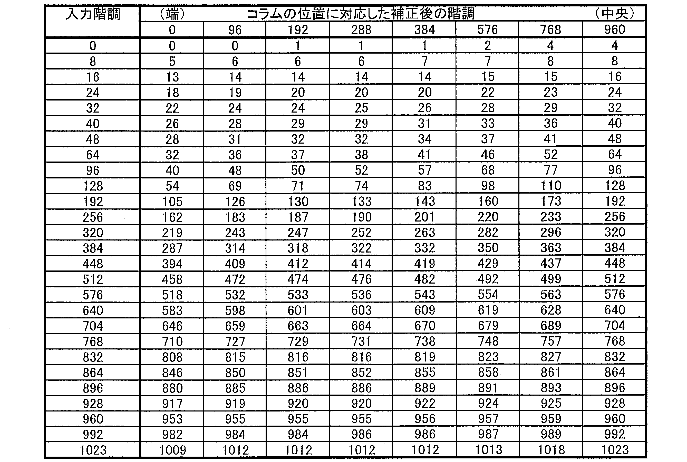
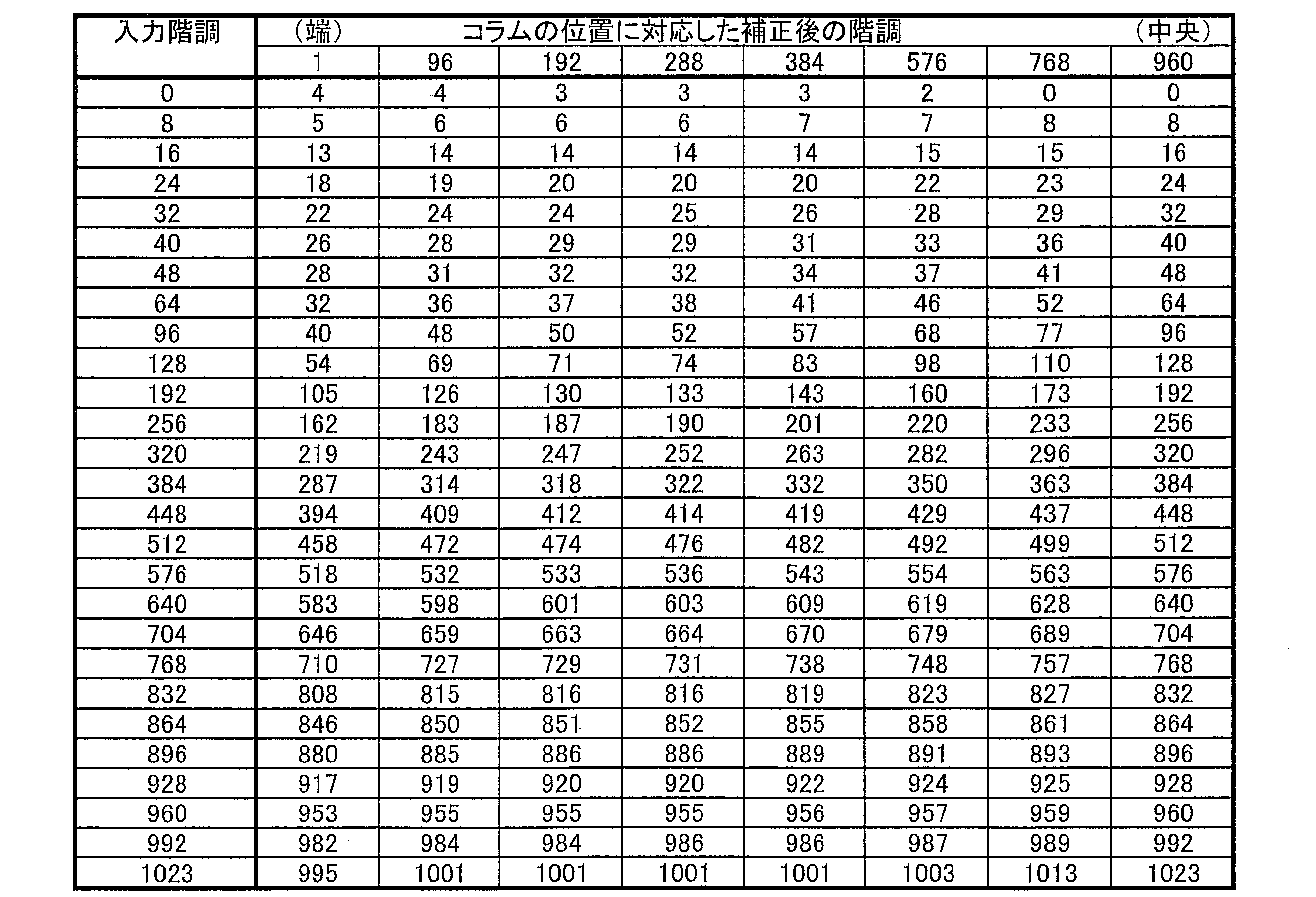
- Table 3 shows a look-up table for positive tone data
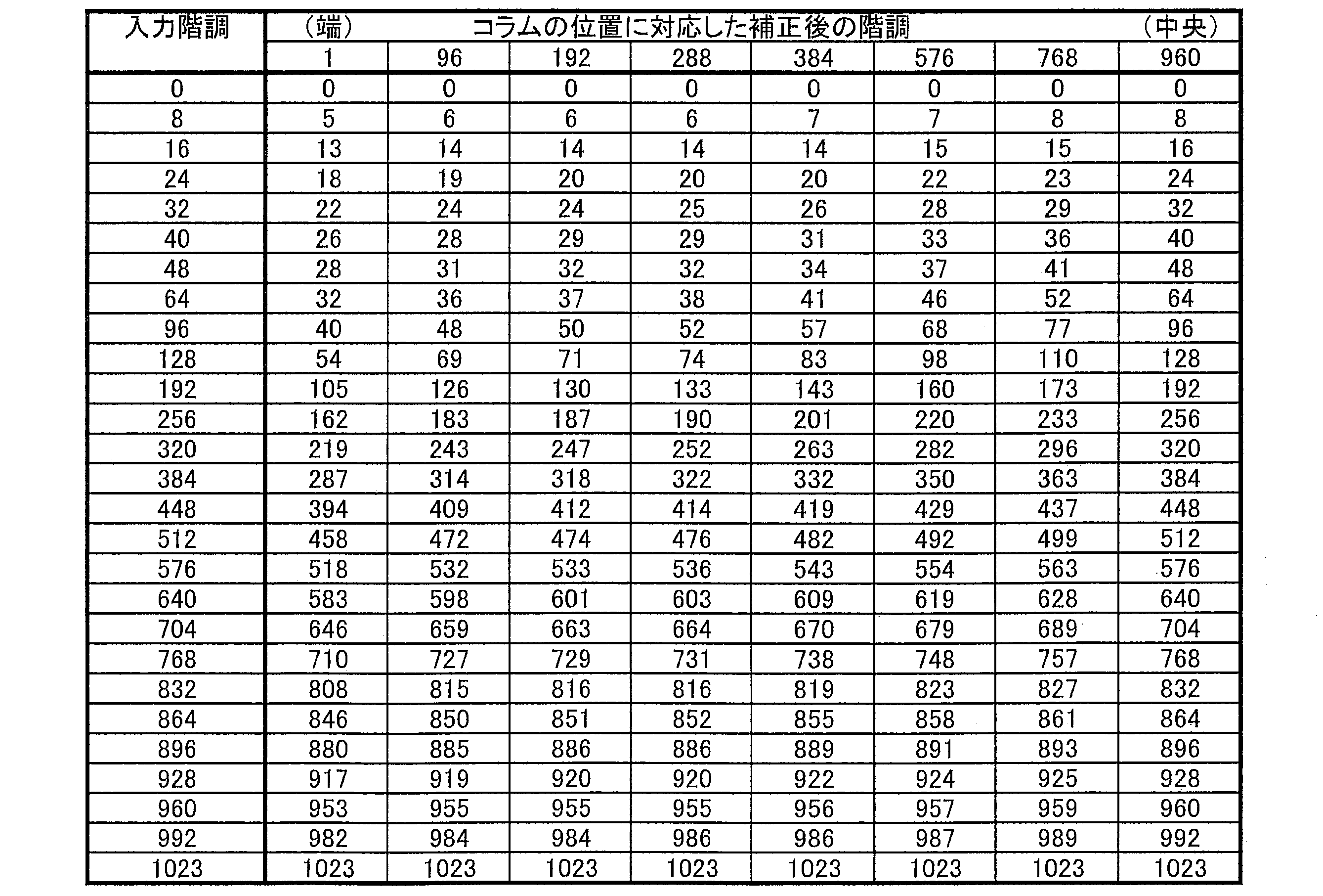
- Table 4 shows a look-up table for negative tone data.
- Tables 3 and 4 the number of bits representing gradation data and the resolution of the display panel are the same as those in Tables 1 and 2.
- the same gradation data supplied to the ⁇ Vd correction unit 51c is supplied to the pixel electrode as the same data signal potential on the entire panel surface, and the same positive polarity gradation data. Since the effective value of the voltage applied to the liquid crystal is equal to the negative gradation data, a uniform display quality can be provided over the entire panel surface.
- FIG. 2 is a diagram for explaining gradation correction according to the second embodiment.
- the meanings of the vertical axis and horizontal axis of the graph are the same as those in FIG.
- the gradation data is corrected to “255” at the position. In this case, the correction amount of all the gradation data in the panel center C is zero.
- the pixel electrode potential passes through a point of the potential VH255 at the panel center C, and the potential of VH255 ′ that becomes a potential lower by the difference of the voltage ⁇ Vd from the panel center C corresponding to the position of each column. From the curve, the potential decreases by the voltage ⁇ Vd at the panel center C.
- the pixel electrode potential is desired to be evenly aligned in the plane after the pull-in phenomenon occurs, but the correction amount at the column position in the center C of the panel with respect to the input gradation data “255”. Is corrected to zero, that is, the data signal potential is set to VL255. Then, only the correction amount corresponding to the difference of the voltage ⁇ Vd from the panel center C corresponding to the position of each column is subtracted from the panel center C to the panel both ends A through the panel middle B. As a result, correction for reducing the gradation data is performed. In this case, the pixel electrode potential after the pull-in phenomenon occurs is lower than the potential corresponding to the highest gradation data at the position of each column by the voltage ⁇ Vd at the panel center C.
- the pixel electrode potential is not uniform in the plane after the pull-in phenomenon occurs, but in order to set the maximum value at the position of each column,
- the gradation data is corrected to “0” in FIG. In this case, the correction amount of all the gradation data in the panel center C is zero.
- the pixel electrode potential after the pull-in phenomenon occurs is a curve of VL0 ′ that passes through the point of the potential VL0 of the panel center C and becomes a potential lower by the difference of the voltage ⁇ Vd from the panel center C corresponding to the position of each column. Therefore, the voltage ⁇ Vd at the panel center C decreases.
- the common electrode potential Vcom is set to a potential that equally divides between a potential that is lower than the potential VH0 by the voltage ⁇ Vd at the panel center C and a potential that is lower than the potential VL0 ′ by the voltage ⁇ Vd at the panel center C. ing. Further, in this embodiment, the common electrode potential Vcom is obtained when the positive polarity gradation data and the negative polarity gradation data having the same magnitude are focused on the panel central portion C. Between a potential ⁇ Vd at the panel center C lower than the data signal potential corresponding to the tone data and a potential lower by a voltage ⁇ Vd at the panel center C than the data signal potential corresponding to the negative gradation data. The potential is equally divided.
- the output gradation width that can be displayed on the picture element PIX in the center C of the panel after the pull-in phenomenon occurs corresponds to the voltage of the difference between the potential VH255 and the potential VH0 for the positive gradation data.
- the gradation width Rvp is the gradation width Rvn corresponding to the voltage of the difference between the potential VL0 and the potential VL255 for the negative gradation data. Note that the gradient of the gradation in each of the gradation width Rvp and the gradation width Rvn is arbitrarily designed.
- the corrected minimum positive gradation data of the panel central portion C is higher by cp1 than in FIG.
- the positive polarity minimum gradation data in FIG. The same applies to the panel middle part B.
- gradation data is lost even at the highest gradation side of the panel middle portion B and the panel center portion C, but not lost in FIG.
- the characteristics of the positive polarity gradation data are the same for the negative polarity gradation data.
- the gradation widths Rvp and Rvn are larger in FIG. 2 than in FIG. 13 over the entire panel.
- the reproduction area in the center of the display panel is widened, which greatly contributes to improvement of display quality.
- Table 5 shows a look-up table for positive tone data
- Table 6 shows a look-up table for negative tone data.
- Tables 5 and 6 the number of bits representing gradation data and the resolution of the display panel are the same as those in Tables 1 and 2.
- the entire gradation width can be used for display in the center portion of the panel, high display quality can be provided.
- FIG. 3 is a diagram for explaining gradation correction according to the third embodiment.
- the meanings of the vertical axis and horizontal axis of the graph are the same as those in FIG.
- the entire gradation width can be used in the panel center C, and the applied voltage of the liquid crystal after the pull-in phenomenon occurs at every column position on the entire panel surface.
- the tone correction is performed so that the tone data and the negative tone data are equal to each other.
- the input grayscale data “0” is corrected so that the correction amount is zero, that is, the data signal potential is VH0 at the column position in the center C of the panel. Then, over the region from the panel central portion C to the panel central portion C through the panel intermediate portion B, the correction amount is larger than the correction amount corresponding to the difference in voltage ⁇ Vd from the panel central portion C corresponding to the position of each column. Correction for increasing the gradation data is performed by adding the correction amount. In this case, if the potential corresponding to the corrected gradation data is VH0 ′, the pixel electrode potential after the pull-in phenomenon is generated from the potential VH0 ′ through the point of the potential VH0 at the center C of the panel. The voltage decreases by the voltage ⁇ Vd at the panel center C from the curve of the potential VH0 ′′ that decreases by the correction amount corresponding to the difference in voltage ⁇ Vd from the panel center C corresponding to the column position.
- the gradation data is corrected to “255” at the position. In this case, the correction amount of all the gradation data in the panel center C is zero.
- the pixel electrode potential passes through a point of the potential VH255 at the panel center C, and the potential of VH255 ′ that becomes a potential lower by the difference of the voltage ⁇ Vd from the panel center C corresponding to the position of each column. From the curve, the potential decreases by the voltage ⁇ Vd at the panel center C.
- the input gradation data “255” is corrected so that the correction amount is zero, that is, the data signal potential is VL255, at the column position in the center C of the panel. Then, over a region from the panel center C to the panel both ends A via the panel middle B, a correction larger than the correction amount corresponding to the difference in ⁇ Vd from the panel center C corresponding to the position of each column. Correction for decreasing the gradation data is performed by subtracting the amount.
- the potential corresponding to the corrected gradation data is VL255 ′
- the pixel electrode potential after the pull-in phenomenon is generated from the potential VL255 ′ through the point of the potential VL255 at the center C of the panel.
- the voltage is decreased by the voltage ⁇ Vd at the panel center C from the curve of the potential VL255 ′′ which is decreased by the correction amount corresponding to the difference in voltage ⁇ Vd from the panel center C corresponding to the column position.
- the input gradation data “0” is corrected so that the correction amount is zero, that is, the data signal potential is VL0 at the column position in the center C of the panel. Then, in the region from the panel center C to the panel center C via the panel middle B, the correction amount is smaller than the correction amount corresponding to the difference in voltage ⁇ Vd from the panel center C corresponding to the position of each column. Correction for increasing the gradation data is performed by adding the correction amount. In this case, if the potential corresponding to the corrected gradation data is VL0 ′, the pixel electrode potential after the pull-in phenomenon is generated from the potential VL0 ′ through the point of the potential VL0 in the center C of the panel. The voltage is lowered by the voltage ⁇ Vd at the panel center C from the curve of the potential VL0 ′′ which is decreased by a correction amount corresponding to the difference in voltage ⁇ Vd from the panel center C corresponding to the column position.
- the common electrode potential Vcom is set to a potential that equally divides between a potential that is lower than the potential VH0 by the voltage ⁇ Vd at the panel center C and a potential that is lower than the potential VL0 ′ by the voltage ⁇ Vd at the panel center C. ing. Further, in this embodiment, the common electrode potential Vcom is obtained when the positive polarity gradation data and the negative polarity gradation data having the same magnitude are focused on the panel central portion C. Between a potential ⁇ Vd at the panel center C lower than the data signal potential corresponding to the tone data and a potential lower by a voltage ⁇ Vd at the panel center C than the data signal potential corresponding to the negative gradation data. The potential is equally divided.
- the difference between the pixel electrode potential corresponding to the corrected positive polarity gradation data and the common electrode potential Vcom, and the corrected negative polarity gradation data are supported.
- the difference between the pixel electrode potential and the common electrode potential Vcom can be made equal to each other.
- the output gradation width that can be displayed on the picture element PIX in the center C of the panel after the pull-in phenomenon occurs corresponds to the voltage of the difference between the potential VH255 and the potential VH0 for the positive gradation data.
- the gradation width Rvp is the gradation width Rvn corresponding to the voltage of the difference between the potential VL0 and the potential VL255 for the negative gradation data. Note that the gradient of the gradation in each of the gradation width Rvp and the gradation width Rvn is arbitrarily designed.
- the corrected minimum gradation data of the positive polarity at the center C of the panel is higher by cp1 than in FIG.
- the gradation data is lost on the highest gradation side of the panel intermediate portion B and the panel central portion C, but not lost in FIG.
- the characteristics of the positive polarity gradation data are the same for the negative polarity gradation data.
- the gradation widths Rvp and Rvn are larger in FIG. 3 than in FIG.
- the reproduction area in the center of the display panel is widened, which greatly contributes to improvement of display quality.
- Table 7 shows a look-up table for positive tone data
- Table 8 shows a look-up table for negative tone data.
- Tables 7 and 8 the number of bits representing gradation data and the resolution of the display panel are the same as those in Tables 1 and 2.
- the entire gradation width can be used for display in the panel central portion C, high display quality can be provided. Furthermore, at each column position, the difference between the pixel electrode potential corresponding to the corrected positive polarity gradation data and the common electrode potential Vcom, and the pixel electrode potential corresponding to the corrected negative polarity gradation data. And the common electrode potential Vcom can be made equal to each other.
- FIG. 4 is a diagram for explaining gradation correction according to the fourth embodiment.
- the meanings of the vertical axis and horizontal axis of the graph are the same as those in FIG.
- the gradation data is corrected to “255” at the position. In this case, all the gradation data have zero correction amount.
- the pixel electrode potential passes through a point of the potential VH255 at the panel center C, and the potential of VH255 ′ that becomes a potential lower by the difference of the voltage ⁇ Vd from the panel center C corresponding to the position of each column. From the curve, the potential decreases by the voltage ⁇ Vd at the panel center C.
- the gradation data is corrected to “255”. In this case, all the gradation data have zero correction amount.
- the pixel electrode potential passes through a point of the potential VL255 at the panel center C, and the potential of VL255 ′ that becomes a potential lower by the difference of the voltage ⁇ Vd from the panel center C corresponding to the position of each column. From the curve, the potential decreases by the voltage ⁇ Vd at the panel center C.
- the gradation data is corrected to “0”. In this case, all the gradation data have zero correction amount.
- the pixel electrode potential passes through the point of the potential VL0 of the panel center C, and the potential of VL0 ′ which becomes a potential lower by the difference of the voltage ⁇ Vd from the panel center C corresponding to the position of each column. From the curve, the potential decreases by the voltage ⁇ Vd at the panel center C.
- the common electrode potential Vcom is set to a potential that equally divides between a potential that is lower than the potential VH0 by the voltage ⁇ Vd at the panel center C and a potential that is lower than the potential VL0 ′ by the voltage ⁇ Vd at the panel center C. ing. Further, in this embodiment, the common electrode potential Vcom is obtained when the positive polarity gradation data and the negative polarity gradation data are equal in magnitude at each column position on the entire panel surface. Between a potential that is lower by a voltage ⁇ Vd at the column position than the data signal potential corresponding to the grayscale data and a potential that is lower by a voltage ⁇ Vd at the column position than the data signal potential corresponding to the negative grayscale data. The potential is equally divided.
- the difference between the pixel electrode potential corresponding to the corrected positive polarity gradation data and the common electrode potential at the position of each column, and the corrected negative polarity gradation data can be made equal to each other.
- the output gradation width that can be displayed on the picture element PIX in the center C of the panel after the pull-in phenomenon occurs corresponds to the voltage of the difference between the potential VH255 and the potential VH0 for the positive gradation data.
- the gradation width Rvp is the gradation width Rvn corresponding to the voltage of the difference between the potential VL0 and the potential VL255 for the negative gradation data. Note that the gradient of the gradation in each of the gradation width Rvp and the gradation width Rvn is arbitrarily designed.
- the corrected minimum positive gradation data of the center C of the panel is higher by cp1 than in FIG.
- gradation data is lost on the highest gradation side of the panel middle part B and the panel center part C, but not lost in FIG.
- the characteristics of the positive polarity gradation data are the same for the negative polarity gradation data.
- the gradation widths Rvp and Rvn are larger in FIG. 4 than in FIG.
- the reproduction area in the center of the display panel is widened, which greatly contributes to improvement of display quality.
- the relationship between the input gradation data and the corrected gradation data provided in the memory 51e is stored. This will be described using the look-up table.
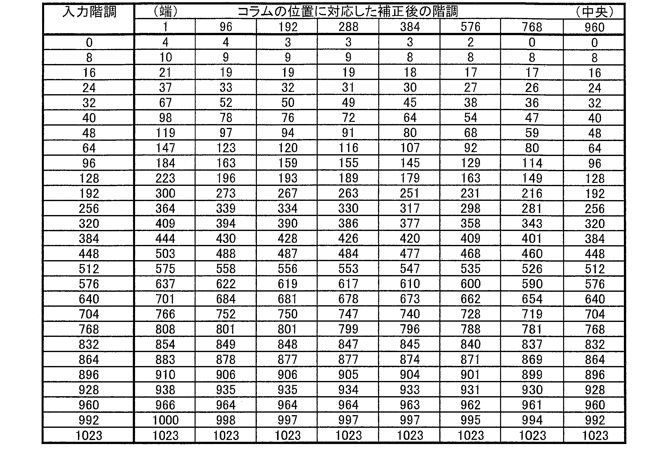
- Table 9 shows a look-up table for positive tone data
- Table 10 shows a look-up table for negative tone data.
- Tables 9 and 10 the number of bits representing gradation data and the resolution of the display panel are the same as those in Tables 1 and 2.
- the entire gradation width can be used for display on the entire panel surface, high display quality can be provided.
- the positive polarity minimum gradation data and the negative polarity minimum gradation are supplied to the gradation data (first gradation data) supplied to the column position in the center of the panel.
- gradation correction was performed with the correction amount set to zero.
- the present invention is not limited to this, and the position of the column at the center of the panel is set so as to include a plurality of columns, or at least one column constituting a part of all the columns of the first to the first embodiments. It is also possible to perform the same processing as in step 3.
- the data signal line driver may include the gradation correction function.
- the gradation correction may be performed on the gradation data before being converted into the data signal.
- the present invention is not limited to this, and can be applied to all phenomena in which in-plane distribution occurs in the pixel electrode potential. is there.
- two gate drivers GD1 and GD2 are prepared and gate pulses are supplied from both ends of each gate bus line GL.
- the present invention is not limited to this. You may make it supply a gate pulse from the predetermined one end with respect to the gate bus line GL.
- the above example can be applied according to the distribution of the voltage ⁇ Vd in the panel surface generated when the gate pulse is supplied from one end.
- the present invention can be applied to all phenomena in which an in-plane distribution occurs in the pixel electrode potential, even when a gate pulse is supplied from one end, what is the in-plane distribution of the voltage ⁇ Vd? Arbitrary different in-plane distributions can be assumed, and the gradation correction according to the panel positions of the panel end A, the panel intermediate B, and the panel center C as in the above-described embodiment is naturally possible. .
- the correction amount corresponding to the position of a part of the column is stored in the lookup table in the memory 51e, and the lookup table for the input gradation data corresponding to the position of the part of the column is stored. Tone correction is performed using the stored value as the correction amount. For input tone data corresponding to the positions of other columns, the correction amount is obtained by interpolation using the stored value in the lookup table. Tone correction may be performed. In this way, the value of the correction amount stored in the lookup table can be reduced, so that the display device can be reduced in size.
- the present invention can be suitably used for a television device or a monitor device.
- Liquid crystal display device (display device) 2 Display panel 5 Display controller 51c ⁇ Vd correction unit (correction unit) GL gate bus line SL source bus line SD1, SD2 Source driver (display driver) P picture element Vcom common electrode potential
Landscapes
- Engineering & Computer Science (AREA)
- Chemical & Material Sciences (AREA)
- Crystallography & Structural Chemistry (AREA)
- Physics & Mathematics (AREA)
- Computer Hardware Design (AREA)
- General Physics & Mathematics (AREA)
- Theoretical Computer Science (AREA)
- Multimedia (AREA)
- Signal Processing (AREA)
- Control Of Indicators Other Than Cathode Ray Tubes (AREA)
- Liquid Crystal Display Device Control (AREA)
- Liquid Crystal (AREA)
Abstract
Description
ΔVd=(Cgd/Cpix)・Vgp-p
=(Cgd/Cpix)・(Vgh-Vgl) ・・・(1)
と表される。図8において寄生容量として容量Cgdのみを考慮した場合にはCpix=Clc+Cs+Cgdである。


2 表示パネル
5 表示コントローラ
51c ΔVd補正部(補正部)
GL ゲートバスライン
SL ソースバスライン
SD1、SD2
ソースドライバ(表示ドライバ)
P 絵素
Vcom コモン電極電位
Claims (22)
- アクティブマトリクス型の表示装置であって、
データ信号に変換される前の階調データに対して、表示パネル上のデータ信号を供給する各コラムの位置に対応した補正量で階調補正を行う補正部を備えており、
上記補正部は、入力される上記階調データのうち、全コラムの一部をなす少なくとも1つのコラムに供給する第1の階調データの、少なくとも、正極性の最も低いデータ信号電位に対応する階調データおよび負極性の最も低いデータ信号電位に対応する階調データに対しては上記補正量をゼロとして上記階調補正を行うことを特徴とする表示装置。 - 上記補正部は、入力される上記階調データのうち、全コラムのうちの中央に位置する1つ以上のコラムに供給する第1の階調データの、少なくとも、正極性の最も低いデータ信号電位に対応する階調データおよび負極性の最も低いデータ信号電位に対応する階調データに対しては上記補正量をゼロとして上記階調補正を行うことを特徴とする請求項1に記載の表示装置。
- 上記階調補正後の上記第1の階調データに対応する正極性の最も高いデータ信号電位は、上記階調補正後の上記第1の階調データ以外の上記階調データに対応する正極性の最も高いデータ信号電位よりも低く、
上記階調補正後の上記第1の階調データに対応する負極性の最も高いデータ信号電位は、上記階調補正後の上記第1の階調データ以外の上記階調データに対応する負極性の最も高いデータ信号電位よりも低いことを特徴とする請求項1または2に記載の表示装置。 - 全てのコラムについて、正極性の最も高いデータ信号電位に対応する階調データに対しては、上記補正量をゼロとして上記階調補正を行い、
全てのコラムについて、負極性の最も高いデータ信号電位に対応する階調データに対しては、上記補正量をゼロとして上記階調補正を行うことを特徴とする請求項1または2に記載の表示装置。 - 全てのコラムについて、正極性の最も高いデータ信号電位に対応する階調データに対しては、上記補正量をゼロとして上記階調補正を行い、
上記階調補正後の上記第1の階調データに対応する負極性の最も高いデータ信号電位は、上記階調補正後の上記第1の階調データ以外の上記階調データに対応する負極性の最も高いデータ信号電位よりも高いことを特徴とする請求項1または2に記載の表示装置。 - アクティブマトリクス型の表示装置であって、
データ信号に変換される前の階調データに対して、表示パネル上のデータ信号を供給する各コラムの位置に対応した補正量で階調補正を行う補正部を備えており、
上記補正部は、入力される上記階調データのうち、全コラムの、正極性の最も低いデータ信号電位に対応する階調データ、負極性の最も低いデータ信号電位に対応する階調データ、正極性の最も高いデータ信号電位に対応する階調データ、および、負極性の最も高いデータ信号電位に対応する階調データに対しては上記補正量をゼロとして上記階調補正を行うことを特徴とする表示装置。 - 上記データ信号に変換される前の階調データは、表示ドライバに供給される前の階調データであることを特徴とする請求項1から6までのいずれか1項に記載の表示装置。
- 各ゲートバスラインに、上記各ゲートバスラインの両端からゲートパルスを供給することを特徴とする請求項1から7までのいずれか1項に記載の表示装置。
- 各ゲートバスラインに、全ての上記ゲートバスラインに対する所定の片端からゲートパルスを供給することを特徴とする請求項1から7までのいずれか1項に記載の表示装置。
- 上記補正量は、上記各コラムの位置に対応した引き込み電圧の大きさに対応していることを特徴とする請求項1から9までのいずれか1項に記載の表示装置。
- 一部の上記コラムの位置に対応した上記補正量をルックアップテーブルに格納しており、
上記一部の上記コラムの位置に対応した上記階調データに対しては、上記補正量として上記ルックアップテーブルの格納値を用いて上記階調補正を行い、
他の上記コラムの位置に対応した上記階調データに対しては、上記補正量を上記ルックアップテーブルの格納値を用いた補間演算により求めて上記階調補正を行うことを特徴とする請求項1から10までのいずれか1項に記載の表示装置。 - アクティブマトリクス型の表示装置を駆動する表示装置の駆動方法であって、
データ信号に変換される前の階調データに対して、表示パネル上のデータ信号を供給する各コラムの位置に対応した補正量で階調補正を行い、
上記階調補正に供給される上記階調データのうち、全コラムの一部をなす少なくとも1つのコラムに供給する第1の階調データの、少なくとも、正極性の最も低いデータ信号電位に対応する階調データおよび負極性の最も高いデータ信号電位に対応する階調データに対しては上記補正量をゼロとして上記階調補正を行うことを特徴とする表示装置の駆動方法。 - 上記階調補正に供給される上記階調データのうち、全コラムのうちの中央に位置する1つ以上のコラムに供給する第1の階調データの、少なくとも、正極性の最も低いデータ信号電位に対応する階調データおよび負極性の最も低いデータ信号電位に対応する階調データに対しては上記補正量をゼロとして上記階調補正を行うことを特徴とする請求項12に記載の表示装置の駆動方法。
- 上記階調補正後の上記第1の階調データに対応する正極性の最も高いデータ信号電位は、上記階調補正後の上記第1の階調データ以外の上記階調データに対応する正極性の最も高いデータ信号電位よりも低く、
上記階調補正後の上記第1の階調データに対応する負極性の最も高いデータ信号電位は、上記階調補正後の上記第1の階調データ以外の上記階調データに対応する負極性の最も高いデータ信号電位よりも低いことを特徴とする請求項12または13に記載の表示装置の駆動方法。 - 全てのコラムについて、正極性の最も高いデータ信号電位に対応する階調データに対しては、上記補正量をゼロとして上記階調補正を行い、
全てのコラムについて、負極性の最も高いデータ信号電位に対応する階調データに対しては、上記補正量をゼロとして上記階調補正を行うことを特徴とする請求項12または13に記載の表示装置の駆動方法。 - 全てのコラムについて、正極性の最も高いデータ信号電位に対応する階調データに対しては、上記補正量をゼロとして上記階調補正を行い、
上記階調補正後の上記第1の階調データに対応する負極性の最も高いデータ信号電位は、上記階調補正後の上記第1の階調データ以外の上記階調データに対応する負極性の最も高いデータ信号電位よりも高くなるように上記階調補正を行うことを特徴とする請求項12または13に記載の表示装置の駆動方法。 - アクティブマトリクス型の表示装置を駆動する表示装置の駆動方法であって、
データ信号に変換される前の階調データに対して、表示パネル上のデータ信号を供給する各コラムの位置に対応した補正量で階調補正を行い、
上記階調補正に供給される上記階調データのうち、全コラムの、正極性の最も低いデータ信号電位に対応する階調データ、負極性の最も低いデータ信号電位に対応する階調データ、正極性の最も高いデータ信号電位に対応する階調データ、および、負極性の最も高いデータ信号電位に対応する階調データに対しては上記補正量をゼロとして上記階調補正を行うことを特徴とする表示装置の駆動方法。 - 上記データ信号に変換される前の階調データは、表示ドライバに供給される前の階調データであることを特徴とする請求項12から17までのいずれか1項に記載の表示装置の駆動方法。
- 各ゲートバスラインに、上記各ゲートバスラインの両端からゲートパルスを供給することを特徴とする請求項12から18までのいずれか1項に記載の表示装置の駆動方法。
- 各ゲートバスラインに、上記各ゲートバスラインの片端からゲートパルスを供給することを特徴とする請求項12から18までのいずれか1項に記載の表示装置の駆動方法。
- 上記補正量は、上記各コラムの位置に対応した引き込み電圧の大きさに対応していることを特徴とする請求項12から20までのいずれか1項に記載の表示装置の駆動方法。
- 一部の上記コラムの位置に対応した上記補正量をルックアップテーブルに格納しており、
上記一部の上記コラムの位置に対応した上記階調データに対しては、上記補正量として上記ルックアップテーブルの格納値を用いて上記階調補正を行い、
他の上記コラムの位置に対応した上記階調データに対しては、上記補正量を上記ルックアップテーブルの格納値を用いた補間演算により求めて上記階調補正を行うことを特徴とする請求項12から21までのいずれか1項に記載の表示装置の駆動方法。
Priority Applications (2)
| Application Number | Priority Date | Filing Date | Title |
|---|---|---|---|
| US12/998,698 US8698850B2 (en) | 2008-12-25 | 2009-08-25 | Display device and method for driving same |
| CN200980147796.0A CN102265327B (zh) | 2008-12-25 | 2009-08-25 | 显示装置和显示装置的驱动方法 |
Applications Claiming Priority (2)
| Application Number | Priority Date | Filing Date | Title |
|---|---|---|---|
| JP2008-330865 | 2008-12-25 | ||
| JP2008330865 | 2008-12-25 |
Publications (1)
| Publication Number | Publication Date |
|---|---|
| WO2010073775A1 true WO2010073775A1 (ja) | 2010-07-01 |
Family
ID=42287402
Family Applications (1)
| Application Number | Title | Priority Date | Filing Date |
|---|---|---|---|
| PCT/JP2009/064786 Ceased WO2010073775A1 (ja) | 2008-12-25 | 2009-08-25 | 表示装置および表示装置の駆動方法 |
Country Status (3)
| Country | Link |
|---|---|
| US (1) | US8698850B2 (ja) |
| CN (1) | CN102265327B (ja) |
| WO (1) | WO2010073775A1 (ja) |
Cited By (5)
| Publication number | Priority date | Publication date | Assignee | Title |
|---|---|---|---|---|
| US20120007894A1 (en) * | 2010-07-09 | 2012-01-12 | Yong-Hwan Shin | Method of Driving Display Panel and Display Apparatus for Performing the Same |
| US20120229523A1 (en) * | 2011-03-10 | 2012-09-13 | Panasonic Liquid Crystal Display Co., Ltd. | Liquid crystal display device |
| US9013517B2 (en) | 2011-03-10 | 2015-04-21 | Panasonic Liquid Crystal Display Co., Ltd. | Liquid crystal display device |
| WO2018061093A1 (ja) * | 2016-09-27 | 2018-04-05 | 堺ディスプレイプロダクト株式会社 | 液晶表示装置の輝度むら補正方法及び補正データ生成装置 |
| JPWO2016207982A1 (ja) * | 2015-06-23 | 2018-05-24 | 堺ディスプレイプロダクト株式会社 | 液晶表示装置及び液晶表示装置の駆動方法 |
Families Citing this family (19)
| Publication number | Priority date | Publication date | Assignee | Title |
|---|---|---|---|---|
| JP2012189765A (ja) | 2011-03-10 | 2012-10-04 | Panasonic Liquid Crystal Display Co Ltd | 液晶表示装置 |
| JP2014130336A (ja) * | 2012-11-30 | 2014-07-10 | Semiconductor Energy Lab Co Ltd | 表示装置 |
| TWI603305B (zh) * | 2013-09-27 | 2017-10-21 | 鴻海精密工業股份有限公司 | 顯示裝置、拼接式顯示器及顯示面板 |
| KR102219132B1 (ko) | 2014-01-27 | 2021-02-23 | 삼성디스플레이 주식회사 | 액정 표시 장치 |
| CN103985356B (zh) * | 2014-05-26 | 2016-06-15 | 合肥工业大学 | 一种oled灰阶丢失补偿的方法 |
| CN104347048B (zh) * | 2014-11-21 | 2016-08-03 | 深圳市华星光电技术有限公司 | 液晶显示面板及其灰阶电压补偿方法 |
| JP6220466B2 (ja) * | 2014-12-18 | 2017-10-25 | 堺ディスプレイプロダクト株式会社 | 液晶表示装置及び液晶表示装置の駆動方法 |
| KR102324238B1 (ko) * | 2015-06-29 | 2021-11-10 | 삼성디스플레이 주식회사 | 얼룩 검사 장치 및 이의 구동 방법 |
| CN105278142A (zh) * | 2015-11-12 | 2016-01-27 | 深圳市华星光电技术有限公司 | 液晶显示面板及液晶显示装置 |
| KR102468727B1 (ko) | 2015-12-28 | 2022-11-21 | 엘지디스플레이 주식회사 | 타이밍 컨트롤러, 데이터 드라이버, 표시장치 및 그 구동방법 |
| CN105957479B (zh) * | 2016-05-31 | 2019-09-10 | 深圳市华星光电技术有限公司 | 接口装置及具有该接口装置的液晶显示器 |
| CN106297709A (zh) * | 2016-09-09 | 2017-01-04 | 合肥鑫晟光电科技有限公司 | 显示面板、补偿装置、显示装置和公共电极电压补偿方法 |
| CN106898323B (zh) * | 2017-04-07 | 2019-06-07 | 深圳市华星光电技术有限公司 | 一种液晶面板及其灰阶电压补偿方法、及其驱动电路 |
| KR102390476B1 (ko) * | 2017-08-03 | 2022-04-25 | 엘지디스플레이 주식회사 | 유기발광 표시장치 및 유기발광 표시장치의 데이터 처리방법 |
| CN113593494B (zh) * | 2021-07-19 | 2022-07-12 | Tcl华星光电技术有限公司 | 显示补偿方法及装置、显示面板 |
| US11823637B2 (en) | 2021-12-29 | 2023-11-21 | Novatek Microelectronics Corp. | Timing control circuit and operation method thereof |
| TWI804140B (zh) * | 2021-12-29 | 2023-06-01 | 聯詠科技股份有限公司 | 時序控制電路及時序控制電路的操作方法 |
| CN115497428B (zh) * | 2022-08-17 | 2023-10-17 | Tcl华星光电技术有限公司 | 亮度补偿方法、可读存储介质以及显示装置 |
| CN119998862A (zh) * | 2022-12-22 | 2025-05-13 | 谷歌有限责任公司 | 显示器外围的可变亮度调光 |
Citations (6)
| Publication number | Priority date | Publication date | Assignee | Title |
|---|---|---|---|---|
| JP2000098343A (ja) * | 1998-09-28 | 2000-04-07 | Toshiba Corp | 色ムラ補正装置 |
| JP2002055675A (ja) * | 1999-09-17 | 2002-02-20 | Matsushita Electric Ind Co Ltd | 画像表示装置 |
| JP2002123209A (ja) * | 2000-10-17 | 2002-04-26 | Matsushita Electric Ind Co Ltd | 表示装置および映像信号補正装置 |
| JP2002140029A (ja) * | 2000-11-06 | 2002-05-17 | Semiconductor Energy Lab Co Ltd | 表示装置の駆動回路およびその駆動方法 |
| JP2007025239A (ja) * | 2005-07-15 | 2007-02-01 | Casio Comput Co Ltd | 表示駆動装置及び表示装置 |
| JP2008145471A (ja) * | 2006-12-06 | 2008-06-26 | Hitachi Displays Ltd | 画像補正方法及び画像表示装置 |
Family Cites Families (42)
| Publication number | Priority date | Publication date | Assignee | Title |
|---|---|---|---|---|
| JPH01147975A (ja) | 1987-12-04 | 1989-06-09 | Stanley Electric Co Ltd | 液晶テレビジョン |
| JPH06222330A (ja) | 1993-01-25 | 1994-08-12 | Hitachi Ltd | 液晶表示装置 |
| JPH07175454A (ja) | 1993-10-25 | 1995-07-14 | Toshiba Corp | 表示制御装置および表示制御方法 |
| JPH07134572A (ja) | 1993-11-11 | 1995-05-23 | Nec Corp | アクティブマトリクス型液晶表示装置の駆動回路 |
| JP3516382B2 (ja) | 1998-06-09 | 2004-04-05 | シャープ株式会社 | 液晶表示装置及びその駆動方法並びに走査線駆動回路 |
| KR100303206B1 (ko) | 1998-07-04 | 2001-11-30 | 구본준, 론 위라하디락사 | 도트 인버젼 방식 액정 패널 구동 장치 |
| US6310594B1 (en) * | 1998-11-04 | 2001-10-30 | International Business Machines Corporation | Driving method and circuit for pixel multiplexing circuits |
| JP2001051252A (ja) | 1999-08-06 | 2001-02-23 | Matsushita Electric Ind Co Ltd | 液晶表示装置の駆動方法 |
| TW501079B (en) | 1999-09-17 | 2002-09-01 | Matsushita Electric Industrial Co Ltd | Image display device |
| US7129918B2 (en) | 2000-03-10 | 2006-10-31 | Semiconductor Energy Laboratory Co., Ltd. | Electronic device and method of driving electronic device |
| US20020030647A1 (en) | 2000-06-06 | 2002-03-14 | Michael Hack | Uniform active matrix oled displays |
| WO2002063384A1 (en) | 2001-02-05 | 2002-08-15 | Matsushita Electric Industrial Co., Ltd. | Liquid crystal display unit and driving method therefor |
| JP2002251170A (ja) | 2001-02-23 | 2002-09-06 | Matsushita Electric Ind Co Ltd | 液晶表示装置 |
| JP4218249B2 (ja) | 2002-03-07 | 2009-02-04 | 株式会社日立製作所 | 表示装置 |
| KR100477986B1 (ko) | 2002-04-12 | 2005-03-23 | 삼성에스디아이 주식회사 | 유기 전계발광 표시장치 및 이의 구동방법 |
| JP4342200B2 (ja) | 2002-06-06 | 2009-10-14 | シャープ株式会社 | 液晶表示装置 |
| JP3954979B2 (ja) | 2003-03-25 | 2007-08-08 | 三洋電機株式会社 | 投写型映像表示装置、投写型映像表示装置における光偏向装置および直視型映像表示装置 |
| JP3871656B2 (ja) | 2003-05-23 | 2007-01-24 | シャープ株式会社 | 能動行列型液晶表示器及びその駆動方法 |
| JP2004046236A (ja) | 2003-09-05 | 2004-02-12 | Matsushita Electric Ind Co Ltd | 液晶表示装置の駆動方法 |
| KR100688498B1 (ko) | 2004-07-01 | 2007-03-02 | 삼성전자주식회사 | 게이트 드라이버가 내장된 액정 패널 및 이의 구동 방법 |
| JP2006030834A (ja) | 2004-07-21 | 2006-02-02 | International Display Technology Kk | オーバードライブ制御法による駆動方法及びその方法を用いた液晶ディスプレイ |
| KR20060010223A (ko) | 2004-07-27 | 2006-02-02 | 삼성전자주식회사 | 어레이 기판과, 이를 갖는 표시 장치와, 이의 구동 장치및 구동 방법 |
| JP4361844B2 (ja) | 2004-07-28 | 2009-11-11 | 富士通株式会社 | 液晶表示装置 |
| JP2008107369A (ja) | 2005-02-01 | 2008-05-08 | Sharp Corp | 液晶表示装置および液晶表示駆動回路 |
| TWI301603B (en) | 2005-09-02 | 2008-10-01 | Au Optronics Corp | Driving system and method for liquid crystal display |
| FR2894369B1 (fr) | 2005-12-07 | 2008-07-18 | Thales Sa | Procede d'adressage ameliore pour un afficheur matriciel a cristaux liquides |
| TW200739507A (en) | 2006-03-23 | 2007-10-16 | Toshiba Matsushita Display Tec | Liquid crystal display device |
| JP2007286135A (ja) | 2006-04-12 | 2007-11-01 | Toshiba Matsushita Display Technology Co Ltd | 液晶表示装置 |
| JP4400605B2 (ja) * | 2006-09-25 | 2010-01-20 | カシオ計算機株式会社 | 表示駆動装置及び表示装置 |
| WO2008065773A1 (en) | 2006-11-29 | 2008-06-05 | Sharp Kabushiki Kaisha | Liquid crystal display apparatus, liquid crystal display apparatus driving circuit, liquid crystal display apparatus source driver, and liquid crystal display apparatus controller |
| CN100589168C (zh) * | 2006-12-04 | 2010-02-10 | 瀚宇彩晶股份有限公司 | 补偿馈通电压显示装置 |
| KR101351386B1 (ko) | 2007-03-23 | 2014-01-14 | 엘지디스플레이 주식회사 | 액정표시장치 및 이의 구동방법 |
| CN101669162B (zh) | 2007-04-26 | 2012-07-25 | 夏普株式会社 | 液晶显示装置 |
| US8471793B2 (en) | 2007-04-27 | 2013-06-25 | Sharp Kabushiki Kaisha | Liquid crystal display device |
| CN101320179B (zh) | 2007-06-06 | 2011-07-27 | 奇美电子股份有限公司 | 液晶显示装置 |
| CN100492115C (zh) * | 2007-07-12 | 2009-05-27 | 昆山龙腾光电有限公司 | 降低液晶面板闪烁度的调节装置和调节方法及液晶面板 |
| CN101131808B (zh) | 2007-10-15 | 2010-06-09 | 友达光电股份有限公司 | 液晶显示器及其驱动方法 |
| WO2009064364A1 (en) * | 2007-11-13 | 2009-05-22 | Colseq, Inc. | Method and apparatus for reducing erroneous color effects in a field sequential liquid crystal display |
| WO2010038535A1 (ja) | 2008-10-03 | 2010-04-08 | シャープ株式会社 | 液晶表示装置、液晶表示装置の駆動方法、テレビジョン受像機 |
| WO2010061685A1 (ja) | 2008-11-26 | 2010-06-03 | シャープ株式会社 | 液晶表示装置、液晶表示装置の駆動方法、テレビジョン受像機 |
| WO2010061687A1 (ja) | 2008-11-26 | 2010-06-03 | シャープ株式会社 | 液晶表示装置、液晶表示装置の駆動方法、テレビジョン受像機 |
| US8878760B2 (en) | 2008-11-26 | 2014-11-04 | Sharp Kabushiki Kaisha | Liquid crystal display device, method for driving liquid crystal display device, and television receiver |
-
2009
- 2009-08-25 WO PCT/JP2009/064786 patent/WO2010073775A1/ja not_active Ceased
- 2009-08-25 CN CN200980147796.0A patent/CN102265327B/zh not_active Expired - Fee Related
- 2009-08-25 US US12/998,698 patent/US8698850B2/en active Active
Patent Citations (6)
| Publication number | Priority date | Publication date | Assignee | Title |
|---|---|---|---|---|
| JP2000098343A (ja) * | 1998-09-28 | 2000-04-07 | Toshiba Corp | 色ムラ補正装置 |
| JP2002055675A (ja) * | 1999-09-17 | 2002-02-20 | Matsushita Electric Ind Co Ltd | 画像表示装置 |
| JP2002123209A (ja) * | 2000-10-17 | 2002-04-26 | Matsushita Electric Ind Co Ltd | 表示装置および映像信号補正装置 |
| JP2002140029A (ja) * | 2000-11-06 | 2002-05-17 | Semiconductor Energy Lab Co Ltd | 表示装置の駆動回路およびその駆動方法 |
| JP2007025239A (ja) * | 2005-07-15 | 2007-02-01 | Casio Comput Co Ltd | 表示駆動装置及び表示装置 |
| JP2008145471A (ja) * | 2006-12-06 | 2008-06-26 | Hitachi Displays Ltd | 画像補正方法及び画像表示装置 |
Cited By (9)
| Publication number | Priority date | Publication date | Assignee | Title |
|---|---|---|---|---|
| US20120007894A1 (en) * | 2010-07-09 | 2012-01-12 | Yong-Hwan Shin | Method of Driving Display Panel and Display Apparatus for Performing the Same |
| US8872858B2 (en) * | 2010-07-09 | 2014-10-28 | Samsung Display Co., Ltd. | Method of driving display panel and display apparatus for performing the same |
| US20120229523A1 (en) * | 2011-03-10 | 2012-09-13 | Panasonic Liquid Crystal Display Co., Ltd. | Liquid crystal display device |
| CN102682726A (zh) * | 2011-03-10 | 2012-09-19 | 松下液晶显示器株式会社 | 液晶显示装置 |
| US9013517B2 (en) | 2011-03-10 | 2015-04-21 | Panasonic Liquid Crystal Display Co., Ltd. | Liquid crystal display device |
| US9251749B2 (en) * | 2011-03-10 | 2016-02-02 | Panasonic Liquid Crystal Display Co., Ltd. | Liquid crystal display device with grey-scale voltage correction |
| JPWO2016207982A1 (ja) * | 2015-06-23 | 2018-05-24 | 堺ディスプレイプロダクト株式会社 | 液晶表示装置及び液晶表示装置の駆動方法 |
| WO2018061093A1 (ja) * | 2016-09-27 | 2018-04-05 | 堺ディスプレイプロダクト株式会社 | 液晶表示装置の輝度むら補正方法及び補正データ生成装置 |
| US10916211B2 (en) | 2016-09-27 | 2021-02-09 | Sakai Display Products Corporation | Method for correcting luminance non-uniformity in liquid crystal display apparatus, and correction data generation device |
Also Published As
| Publication number | Publication date |
|---|---|
| CN102265327A (zh) | 2011-11-30 |
| US8698850B2 (en) | 2014-04-15 |
| US20110221760A1 (en) | 2011-09-15 |
| CN102265327B (zh) | 2014-10-01 |
Similar Documents
| Publication | Publication Date | Title |
|---|---|---|
| CN102265327B (zh) | 显示装置和显示装置的驱动方法 | |
| KR101069210B1 (ko) | 표시 장치, 액정 모니터, 액정 텔레비젼 수상기 및 표시방법 | |
| US8232946B2 (en) | Liquid crystal display and driving method thereof | |
| JP4400605B2 (ja) | 表示駆動装置及び表示装置 | |
| WO2010087051A1 (ja) | 表示装置および表示装置の駆動方法 | |
| CN102667907B (zh) | 液晶显示装置和液晶显示装置的驱动方法 | |
| JP4330059B2 (ja) | 液晶表示装置及びその駆動制御方法 | |
| US20070279360A1 (en) | Liquid crystal display and driving method thereof | |
| KR102099281B1 (ko) | 액정 표시 장치 및 그 구동 방법 | |
| KR20130084811A (ko) | 표시 패널 및 이의 구동 방법 | |
| TWI757813B (zh) | 抑制顯示面板閃爍之驅動方法及其驅動電路 | |
| US10818258B2 (en) | Liquid crystal display device | |
| US8605019B2 (en) | Display device and display device driving method, and display driving control method | |
| JP2013083804A (ja) | 液晶表示装置 | |
| KR102198250B1 (ko) | 표시 장치 및 그것의 구동 방법 | |
| WO2009133906A1 (ja) | 映像信号線駆動回路および液晶表示装置 | |
| JP2007225861A (ja) | 液晶表示装置 | |
| CN102317841A (zh) | 液晶显示面板和液晶显示装置 | |
| US20180122311A1 (en) | Display control device, liquid crystal display apparatus, and storage medium | |
| CN113870806B (zh) | 用于双闸极显示器的补偿系统和方法 | |
| JP2008216924A (ja) | 表示装置および表示装置の駆動方法 | |
| KR101996339B1 (ko) | 표시 패널 및 이의 구동 방법 | |
| KR20110076647A (ko) | 액정 표시장치 및 그의 구동방법 | |
| JP5024311B2 (ja) | 表示装置の駆動方法 | |
| JP2007025239A (ja) | 表示駆動装置及び表示装置 |
Legal Events
| Date | Code | Title | Description |
|---|---|---|---|
| WWE | Wipo information: entry into national phase |
Ref document number: 200980147796.0 Country of ref document: CN |
|
| 121 | Ep: the epo has been informed by wipo that ep was designated in this application |
Ref document number: 09834581 Country of ref document: EP Kind code of ref document: A1 |
|
| WWE | Wipo information: entry into national phase |
Ref document number: 12998698 Country of ref document: US |
|
| NENP | Non-entry into the national phase |
Ref country code: DE |
|
| NENP | Non-entry into the national phase |
Ref country code: JP |
|
| 122 | Ep: pct application non-entry in european phase |
Ref document number: 09834581 Country of ref document: EP Kind code of ref document: A1 |