WO2010073711A1 - Dispositif de pulvérisation, procédé de pulvérisation et procédé de fabrication de dispositif électronique - Google Patents
Dispositif de pulvérisation, procédé de pulvérisation et procédé de fabrication de dispositif électronique Download PDFInfo
- Publication number
- WO2010073711A1 WO2010073711A1 PCT/JP2009/007278 JP2009007278W WO2010073711A1 WO 2010073711 A1 WO2010073711 A1 WO 2010073711A1 JP 2009007278 W JP2009007278 W JP 2009007278W WO 2010073711 A1 WO2010073711 A1 WO 2010073711A1
- Authority
- WO
- WIPO (PCT)
- Prior art keywords
- substrate
- power
- cathode
- sputtering
- magnetic field
- Prior art date
Links
- 238000004544 sputter deposition Methods 0.000 title claims abstract description 88
- 238000004519 manufacturing process Methods 0.000 title claims description 7
- 238000000034 method Methods 0.000 title description 10
- 239000000758 substrate Substances 0.000 claims abstract description 174
- 230000005291 magnetic effect Effects 0.000 claims abstract description 45
- 238000001514 detection method Methods 0.000 claims abstract description 11
- 238000012545 processing Methods 0.000 claims description 36
- 230000015572 biosynthetic process Effects 0.000 claims description 30
- 239000013077 target material Substances 0.000 claims description 21
- 239000002245 particle Substances 0.000 claims description 10
- 239000000463 material Substances 0.000 claims description 9
- 230000007423 decrease Effects 0.000 claims description 7
- 238000013459 approach Methods 0.000 claims description 6
- 230000005428 wave function Effects 0.000 claims description 6
- 238000000151 deposition Methods 0.000 claims 1
- 230000008021 deposition Effects 0.000 claims 1
- 238000007599 discharging Methods 0.000 claims 1
- 238000009826 distribution Methods 0.000 description 35
- 239000007789 gas Substances 0.000 description 18
- 230000005415 magnetization Effects 0.000 description 17
- 238000010586 diagram Methods 0.000 description 13
- 230000000052 comparative effect Effects 0.000 description 7
- 230000000875 corresponding effect Effects 0.000 description 7
- 238000004364 calculation method Methods 0.000 description 6
- 230000001276 controlling effect Effects 0.000 description 5
- 230000005294 ferromagnetic effect Effects 0.000 description 4
- 239000003302 ferromagnetic material Substances 0.000 description 4
- 239000000696 magnetic material Substances 0.000 description 4
- 230000007246 mechanism Effects 0.000 description 4
- 229910001030 Iron–nickel alloy Inorganic materials 0.000 description 3
- 230000004888 barrier function Effects 0.000 description 3
- 230000003247 decreasing effect Effects 0.000 description 3
- 238000002474 experimental method Methods 0.000 description 3
- 230000008569 process Effects 0.000 description 3
- 230000008859 change Effects 0.000 description 2
- 230000000694 effects Effects 0.000 description 2
- 229910003321 CoFe Inorganic materials 0.000 description 1
- 229910004298 SiO 2 Inorganic materials 0.000 description 1
- XUIMIQQOPSSXEZ-UHFFFAOYSA-N Silicon Chemical compound [Si] XUIMIQQOPSSXEZ-UHFFFAOYSA-N 0.000 description 1
- PNEYBMLMFCGWSK-UHFFFAOYSA-N aluminium oxide Inorganic materials [O-2].[O-2].[O-2].[Al+3].[Al+3] PNEYBMLMFCGWSK-UHFFFAOYSA-N 0.000 description 1
- 230000000903 blocking effect Effects 0.000 description 1
- 238000011109 contamination Methods 0.000 description 1
- 230000002596 correlated effect Effects 0.000 description 1
- 239000002889 diamagnetic material Substances 0.000 description 1
- 230000005684 electric field Effects 0.000 description 1
- 230000005672 electromagnetic field Effects 0.000 description 1
- 239000011261 inert gas Substances 0.000 description 1
- 238000009434 installation Methods 0.000 description 1
- 239000011810 insulating material Substances 0.000 description 1
- 238000012886 linear function Methods 0.000 description 1
- CPLXHLVBOLITMK-UHFFFAOYSA-N magnesium oxide Inorganic materials [Mg]=O CPLXHLVBOLITMK-UHFFFAOYSA-N 0.000 description 1
- 239000000395 magnesium oxide Substances 0.000 description 1
- AXZKOIWUVFPNLO-UHFFFAOYSA-N magnesium;oxygen(2-) Chemical compound [O-2].[Mg+2] AXZKOIWUVFPNLO-UHFFFAOYSA-N 0.000 description 1
- 238000001755 magnetron sputter deposition Methods 0.000 description 1
- 229910044991 metal oxide Inorganic materials 0.000 description 1
- 150000004706 metal oxides Chemical class 0.000 description 1
- 238000012986 modification Methods 0.000 description 1
- 230000004048 modification Effects 0.000 description 1
- 238000005192 partition Methods 0.000 description 1
- 230000002265 prevention Effects 0.000 description 1
- 238000011112 process operation Methods 0.000 description 1
- 238000012887 quadratic function Methods 0.000 description 1
- 238000009717 reactive processing Methods 0.000 description 1
- 238000005546 reactive sputtering Methods 0.000 description 1
- 229910052710 silicon Inorganic materials 0.000 description 1
- 239000010703 silicon Substances 0.000 description 1
- 230000005641 tunneling Effects 0.000 description 1
Images


Classifications
-
- H—ELECTRICITY
- H01—ELECTRIC ELEMENTS
- H01F—MAGNETS; INDUCTANCES; TRANSFORMERS; SELECTION OF MATERIALS FOR THEIR MAGNETIC PROPERTIES
- H01F41/00—Apparatus or processes specially adapted for manufacturing or assembling magnets, inductances or transformers; Apparatus or processes specially adapted for manufacturing materials characterised by their magnetic properties
- H01F41/14—Apparatus or processes specially adapted for manufacturing or assembling magnets, inductances or transformers; Apparatus or processes specially adapted for manufacturing materials characterised by their magnetic properties for applying magnetic films to substrates
- H01F41/18—Apparatus or processes specially adapted for manufacturing or assembling magnets, inductances or transformers; Apparatus or processes specially adapted for manufacturing materials characterised by their magnetic properties for applying magnetic films to substrates by cathode sputtering
-
- C—CHEMISTRY; METALLURGY
- C23—COATING METALLIC MATERIAL; COATING MATERIAL WITH METALLIC MATERIAL; CHEMICAL SURFACE TREATMENT; DIFFUSION TREATMENT OF METALLIC MATERIAL; COATING BY VACUUM EVAPORATION, BY SPUTTERING, BY ION IMPLANTATION OR BY CHEMICAL VAPOUR DEPOSITION, IN GENERAL; INHIBITING CORROSION OF METALLIC MATERIAL OR INCRUSTATION IN GENERAL
- C23C—COATING METALLIC MATERIAL; COATING MATERIAL WITH METALLIC MATERIAL; SURFACE TREATMENT OF METALLIC MATERIAL BY DIFFUSION INTO THE SURFACE, BY CHEMICAL CONVERSION OR SUBSTITUTION; COATING BY VACUUM EVAPORATION, BY SPUTTERING, BY ION IMPLANTATION OR BY CHEMICAL VAPOUR DEPOSITION, IN GENERAL
- C23C14/00—Coating by vacuum evaporation, by sputtering or by ion implantation of the coating forming material
- C23C14/22—Coating by vacuum evaporation, by sputtering or by ion implantation of the coating forming material characterised by the process of coating
- C23C14/34—Sputtering
-
- B—PERFORMING OPERATIONS; TRANSPORTING
- B82—NANOTECHNOLOGY
- B82Y—SPECIFIC USES OR APPLICATIONS OF NANOSTRUCTURES; MEASUREMENT OR ANALYSIS OF NANOSTRUCTURES; MANUFACTURE OR TREATMENT OF NANOSTRUCTURES
- B82Y25/00—Nanomagnetism, e.g. magnetoimpedance, anisotropic magnetoresistance, giant magnetoresistance or tunneling magnetoresistance
-
- C—CHEMISTRY; METALLURGY
- C23—COATING METALLIC MATERIAL; COATING MATERIAL WITH METALLIC MATERIAL; CHEMICAL SURFACE TREATMENT; DIFFUSION TREATMENT OF METALLIC MATERIAL; COATING BY VACUUM EVAPORATION, BY SPUTTERING, BY ION IMPLANTATION OR BY CHEMICAL VAPOUR DEPOSITION, IN GENERAL; INHIBITING CORROSION OF METALLIC MATERIAL OR INCRUSTATION IN GENERAL
- C23C—COATING METALLIC MATERIAL; COATING MATERIAL WITH METALLIC MATERIAL; SURFACE TREATMENT OF METALLIC MATERIAL BY DIFFUSION INTO THE SURFACE, BY CHEMICAL CONVERSION OR SUBSTITUTION; COATING BY VACUUM EVAPORATION, BY SPUTTERING, BY ION IMPLANTATION OR BY CHEMICAL VAPOUR DEPOSITION, IN GENERAL
- C23C14/00—Coating by vacuum evaporation, by sputtering or by ion implantation of the coating forming material
- C23C14/22—Coating by vacuum evaporation, by sputtering or by ion implantation of the coating forming material characterised by the process of coating
- C23C14/34—Sputtering
- C23C14/3464—Sputtering using more than one target
-
- C—CHEMISTRY; METALLURGY
- C23—COATING METALLIC MATERIAL; COATING MATERIAL WITH METALLIC MATERIAL; CHEMICAL SURFACE TREATMENT; DIFFUSION TREATMENT OF METALLIC MATERIAL; COATING BY VACUUM EVAPORATION, BY SPUTTERING, BY ION IMPLANTATION OR BY CHEMICAL VAPOUR DEPOSITION, IN GENERAL; INHIBITING CORROSION OF METALLIC MATERIAL OR INCRUSTATION IN GENERAL
- C23C—COATING METALLIC MATERIAL; COATING MATERIAL WITH METALLIC MATERIAL; SURFACE TREATMENT OF METALLIC MATERIAL BY DIFFUSION INTO THE SURFACE, BY CHEMICAL CONVERSION OR SUBSTITUTION; COATING BY VACUUM EVAPORATION, BY SPUTTERING, BY ION IMPLANTATION OR BY CHEMICAL VAPOUR DEPOSITION, IN GENERAL
- C23C14/00—Coating by vacuum evaporation, by sputtering or by ion implantation of the coating forming material
- C23C14/22—Coating by vacuum evaporation, by sputtering or by ion implantation of the coating forming material characterised by the process of coating
- C23C14/54—Controlling or regulating the coating process
-
- H—ELECTRICITY
- H01—ELECTRIC ELEMENTS
- H01J—ELECTRIC DISCHARGE TUBES OR DISCHARGE LAMPS
- H01J37/00—Discharge tubes with provision for introducing objects or material to be exposed to the discharge, e.g. for the purpose of examination or processing thereof
- H01J37/32—Gas-filled discharge tubes
- H01J37/34—Gas-filled discharge tubes operating with cathodic sputtering
- H01J37/3411—Constructional aspects of the reactor
- H01J37/3414—Targets
- H01J37/3417—Arrangements
-
- H—ELECTRICITY
- H01—ELECTRIC ELEMENTS
- H01J—ELECTRIC DISCHARGE TUBES OR DISCHARGE LAMPS
- H01J37/00—Discharge tubes with provision for introducing objects or material to be exposed to the discharge, e.g. for the purpose of examination or processing thereof
- H01J37/32—Gas-filled discharge tubes
- H01J37/34—Gas-filled discharge tubes operating with cathodic sputtering
- H01J37/3411—Constructional aspects of the reactor
- H01J37/3447—Collimators, shutters, apertures
-
- H—ELECTRICITY
- H01—ELECTRIC ELEMENTS
- H01J—ELECTRIC DISCHARGE TUBES OR DISCHARGE LAMPS
- H01J37/00—Discharge tubes with provision for introducing objects or material to be exposed to the discharge, e.g. for the purpose of examination or processing thereof
- H01J37/32—Gas-filled discharge tubes
- H01J37/34—Gas-filled discharge tubes operating with cathodic sputtering
- H01J37/3411—Constructional aspects of the reactor
- H01J37/345—Magnet arrangements in particular for cathodic sputtering apparatus
- H01J37/3452—Magnet distribution
-
- H—ELECTRICITY
- H01—ELECTRIC ELEMENTS
- H01J—ELECTRIC DISCHARGE TUBES OR DISCHARGE LAMPS
- H01J37/00—Discharge tubes with provision for introducing objects or material to be exposed to the discharge, e.g. for the purpose of examination or processing thereof
- H01J37/32—Gas-filled discharge tubes
- H01J37/34—Gas-filled discharge tubes operating with cathodic sputtering
- H01J37/3411—Constructional aspects of the reactor
- H01J37/345—Magnet arrangements in particular for cathodic sputtering apparatus
- H01J37/3455—Movable magnets
-
- H—ELECTRICITY
- H01—ELECTRIC ELEMENTS
- H01J—ELECTRIC DISCHARGE TUBES OR DISCHARGE LAMPS
- H01J37/00—Discharge tubes with provision for introducing objects or material to be exposed to the discharge, e.g. for the purpose of examination or processing thereof
- H01J37/32—Gas-filled discharge tubes
- H01J37/34—Gas-filled discharge tubes operating with cathodic sputtering
- H01J37/3476—Testing and control
-
- H—ELECTRICITY
- H10—SEMICONDUCTOR DEVICES; ELECTRIC SOLID-STATE DEVICES NOT OTHERWISE PROVIDED FOR
- H10N—ELECTRIC SOLID-STATE DEVICES NOT OTHERWISE PROVIDED FOR
- H10N50/00—Galvanomagnetic devices
- H10N50/01—Manufacture or treatment
-
- H—ELECTRICITY
- H10—SEMICONDUCTOR DEVICES; ELECTRIC SOLID-STATE DEVICES NOT OTHERWISE PROVIDED FOR
- H10N—ELECTRIC SOLID-STATE DEVICES NOT OTHERWISE PROVIDED FOR
- H10N50/00—Galvanomagnetic devices
- H10N50/10—Magnetoresistive devices
-
- H—ELECTRICITY
- H01—ELECTRIC ELEMENTS
- H01F—MAGNETS; INDUCTANCES; TRANSFORMERS; SELECTION OF MATERIALS FOR THEIR MAGNETIC PROPERTIES
- H01F10/00—Thin magnetic films, e.g. of one-domain structure
- H01F10/32—Spin-exchange-coupled multilayers, e.g. nanostructured superlattices
- H01F10/324—Exchange coupling of magnetic film pairs via a very thin non-magnetic spacer, e.g. by exchange with conduction electrons of the spacer
- H01F10/3254—Exchange coupling of magnetic film pairs via a very thin non-magnetic spacer, e.g. by exchange with conduction electrons of the spacer the spacer being semiconducting or insulating, e.g. for spin tunnel junction [STJ]
Definitions
- the present invention relates to a sputtering apparatus, a sputtering method, and an electronic device manufacturing method in which a high voltage is applied to a cathode to generate a discharge with a substrate holder, and a target attached to the cathode is sputtered to form a film on the substrate.
- the present invention relates to a sputtering apparatus, a sputtering method, and an electronic device manufacturing method for forming a film while rotating a substrate along its processing surface.
- sputtering is performed by rotating the substrate at an appropriate speed and maintaining the angle ⁇ of the central axis of the target with respect to the normal of the substrate in a relationship of 15 ° ⁇ ⁇ ⁇ 45 °.
- a method and apparatus have been proposed (see Patent Document 1). According to this sputtering apparatus, a uniform film thickness and film quality can be generated even if the diameter of the target is equal to or smaller than that of the substrate.
- the present invention has been made in view of the above-described problems, and enables a film having excellent in-plane distribution uniformity to be formed, and a sputtering technique that enables easy manufacture of an electronic device having excellent performance. To realize.
- a sputtering apparatus is provided around a substrate holder that holds a substrate rotatably along a surface direction of the processing surface, and is disposed on the processing surface of the substrate.
- a substrate magnetic field forming means for forming a magnetic field, a cathode disposed obliquely opposite the substrate, to which electric power for discharge is applied, a position detecting means for detecting a rotational position of the substrate, and a position detecting means
- Power control means for controlling the power supplied to the cathode according to the detected rotational position.
- the sputtering method of the present invention comprises a position detection means on a cathode disposed obliquely opposite to the substrate while rotating the substrate along the surface direction of the processing surface and forming a magnetic field on the processing surface. Film formation is performed by applying adjusted power according to the detected rotational position of the substrate.
- the substrate is rotated along the surface direction of the processing surface, and a magnetic field is formed on the processing surface.
- a film forming step of forming a film by a sputtering method by applying adjusted electric power according to the rotation position of the substrate detected by the position detecting means.
- a film having excellent uniformity of in-plane distribution of film thickness and composition can be formed, and an electronic device having excellent performance can be manufactured.
- FIG. 1 It is a figure which illustrates sheet resistance distribution (film thickness distribution) on a substrate of this embodiment. It is a figure which illustrates sheet resistance distribution (film thickness distribution) on a substrate of a comparative example. It is a block diagram which shows the structure of the controller of 2nd Embodiment. It is a figure which illustrates the table which prescribes
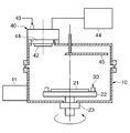
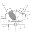
- the sputtering apparatus of this embodiment includes a chamber (reaction vessel) 10 that partitions and forms a processing space.
- An exhaust pump 11 is connected to the chamber 10 through a main valve (not shown) such as a gate valve as an exhaust system that can be evacuated to a desired degree of vacuum.
- a disk-shaped substrate holder 22 that supports a disk-shaped substrate 21 is provided on the upper surface at the lower part of the processing space in the chamber 10.
- the substrate 21 to be processed is usually carried onto the substrate holder 22 through a horizontal slot (not shown) by a handling robot (not shown).
- the substrate holder 22 is a disk-shaped mounting table (stage), and for example, supports the substrate 21 by suction on the upper surface thereof.
- the substrate holder 22 is formed of a conductive member, and also functions as an electrode that generates a discharge with the cathode 41 described later.
- the substrate holder 22 is connected to a rotation drive mechanism (not shown) and is configured to be rotatable around its central axis, and rotates the substrate 21 adsorbed and supported on the mounting surface along the processing surface. It has become. Further, the rotation unit or the rotation drive mechanism of the substrate holder 22 includes a position detection unit that detects the rotation position of the substrate 21 (the rotation position of the substrate holder 22, the rotation position of the magnetic field M formed by the substrate-side magnet 30 described later). (Position sensor) 23 is provided. As the position detector 23, for example, a rotary encoder can be used.
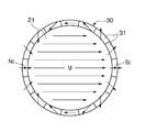
- the outer diameter of the disk-shaped substrate holder 22 is set to be larger than the outer diameter of the substrate 21, and a substrate magnetic field forming unit that forms a magnetic field on the processing surface of the substrate 21 is disposed around the substrate 21 in the substrate holder 22.
- the substrate magnetic field forming unit includes a plurality of magnet pieces 31 made of permanent magnets arranged at equal intervals along the circumferential direction of the substrate holder 22 around the mounting surface of the substrate holder 22.
- the substrate side magnet 30 is configured. That is, the substrate-side magnet 30 is rotatably provided with the substrate 21 on the mounting surface of the substrate holder 22.
- the substrate-side magnet 30 forms a uniform magnetic field having a directivity oriented in one direction within the processing surface along the processing surface of the substrate 21.
- a dipole ring is used, and a plurality of arc-shaped magnet pieces 31 magnetized in different directions are combined in an annular shape to form the magnetic field M in one direction.
- the configuration of the substrate-side magnet 30 is not limited to this, and the magnet may be integrally formed, or may be provided separately from the substrate holder 22 and configured to be rotatable in synchronization with the rotation of the substrate 21. Good.
- the substrate-side magnet 30 is not limited to a permanent magnet, and an electromagnet may be used.
- the substrate 21 is held on the mounting surface of the substrate holder 22 while maintaining a horizontal state.
- a disk-shaped silicon wafer SiO 2 substrate
- the substrate 21 is not limited to this.
- a cathode unit 40 having a cathode 41 for holding a target 42 is disposed obliquely above the substrate holder 22 in the processing space.
- the cathode unit 40 is offset so that the center position of the cathode 41 is shifted from the center axis of the substrate 21 in the surface direction of the substrate 21 so that the cathode 41 is positioned diagonally opposite the substrate 21.
- a magnetron in which a plurality of permanent magnets (cathode side magnets) are arranged is provided on the back surface side of the cathode 41 in the cathode unit 40, and a magnetic field is formed on the surface side of the target 42 attached to the surface of the cathode 41.
- the magnetron may be configured such that a magnet assembly in which permanent magnets are arranged vertically and horizontally on the back surface side of the cathode 41 and a cusp magnetic field is formed on the surface side of the target 42.
- a plate-like target 42 is attached to the surface side of the cathode 41 of the cathode unit 40. That is, the target 42 is provided on the processing space side with respect to the cathode 41 and is arranged facing downward.
- the material of the target 42 varies depending on the type of film formed on the substrate 21.
- a discharge power source 44 that applies a discharge voltage to the cathode 41 is electrically connected to the cathode unit 40.
- the discharge power may be any of high frequency power, DC power, and superposition of high frequency power and DC power.
- a discharge gas introduction system 43 for supplying a discharge processing gas (discharge gas) is connected to the cathode 41 in the vicinity of the cathode unit 40.
- a discharge gas for example, an inert gas such as Ar is used.
- the cathode 41 generates plasma discharge with the substrate holder 22 and can sputter the target 42 attached to the cathode unit 40.
- a shutter 45 is provided in front of the cathode unit 40 for opening or blocking between the substrate 21 and pre-sputtering for removing deposits on the surface of the target 42 before the main sputtering. It is possible.
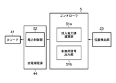
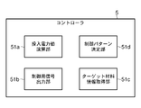
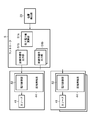
- FIG. 3 is a block diagram showing the controller 5 in the present embodiment.
- the controller 5 of the present embodiment is as shown in FIG. 3, and is configured to include, for example, a general computer and various drivers. Then, a film forming process operation is executed in accordance with a predetermined program or a command from the host apparatus. Specifically, commands are output to the discharge power supply 44, the shutter 45 drive unit, the discharge gas introduction system 43, the exhaust pump 11, the rotation drive mechanism of the substrate holder 22 and the like shown in FIG. Various process conditions such as discharge time, discharge power, target 42 selection and process pressure are controlled according to the command. In addition, output values of sensors such as a pressure gauge (not shown) for measuring the pressure in the chamber 10 and a position detector 23 for detecting the rotational position of the substrate 21 can be acquired, and control according to the state of the apparatus is possible. Is also possible.
- the controller 5 calculates an input power value calculation unit that calculates input power to the cathode 41 so as to increase or decrease the film formation amount according to the rotational position detected by the position detection unit 23. 51a, and a control signal output unit 51b that outputs a control signal for adjusting to the calculated power value (for example, a voltage or current corresponding to the calculated power value).
- the controller 5 has a function of outputting a signal for controlling electric power supplied to the cathode 41 in accordance with the rotational position of the substrate 21 based on the positional relationship between the rotational position of the substrate 21 and the cathode 40 during discharge.
- the power control unit 52 shown in FIG. 3 increases or decreases the power of the discharge power supply 44 based on the control signal input from the control signal output unit 51b, and has the power calculated by the input power value calculation unit 51a. Is output to the cathode 41. Therefore, the cathode 41 receives electric power for discharge corresponding to the rotational position of the substrate 21.
- the input power value can be, for example, a sine wave function of the rotation position of the substrate 21 as shown in FIG. 4, and the correspondence between the rotation position of the substrate 21 and the input power to the cathode 41 is shown in FIG.
- the input power value calculation unit 51a can calculate the input power value.
- the rotational position of the substrate 21 can be determined based on, for example, a line segment that is parallel to the direction of the magnetic field M shown in FIG. 2 and passes through the center of the substrate 21.
- a substrate (wafer) 21 to be processed is placed on a substrate holder 22.
- the substrate 21 is carried onto the substrate holder 22 through a horizontal slot (not shown) using, for example, a handling robot (not shown).
- the inside of the chamber 10 is evacuated to a predetermined degree of vacuum by the exhaust pump 11. Further, a discharge gas such as Ar is introduced into the chamber 10 from the discharge gas introduction system 41.
- a magnetic field is formed on the surface of the target 42 of the cathode unit 40, and electric power for discharge is supplied to generate plasma discharge with the substrate holder 22.
- the target 42 include a target containing a magnetic material such as a Co-containing target, an Fe-containing target, and a Ni-containing target.
- co-sputtering include various magnetic dissimilar materials such as a CoFe layer formed by co-sputtering a Co-containing target and a Fe-containing target, and a NiFe layer formed by co-sputtering a Fe-containing target and a Ni-containing target, Examples include co-sputtering using a target made of a ferromagnetic material.
- a magnetic material containing a diamagnetic material such as B, C, or P can also be used.
- a magnetic field having a direction oriented in one direction is formed on the processing surface of the substrate 21 and the substrate 21 is rotated along the processing surface. Further, during discharge of the cathode unit 40, for example, when the rotational speed is stable, the position detection unit 23 detects the rotation position of the substrate 21 and inputs to the cathode 41 according to the rotation position detected by the position detection unit 23. Adjust the power.
- FIG. 4 is an explanatory diagram showing a control map of input power in the sputtering method using the sputtering apparatus according to the present invention.
- 5 and 6 are diagrams for explaining the principle of this embodiment.
- the input power P to the cathode 41 is a sine wave with respect to the rotation position (rotation angle) ⁇ of the substrate 21.
- the input power is controlled.
- the controller 5 calculates the electric power for discharge to be input to the cathode 41 as a sine wave function of the rotation angle of the substrate 21 based on the above formula (1).
- ⁇ 0 ° ⁇ ⁇ ⁇ 360 °.
- A is the amplitude of the input power
- ⁇ is the phase angle
- B is the center value of the amplitude of the input power
- a is the fluctuation rate of the input power.
- the amplitude A can be arbitrarily set within a range where uniform film formation can be realized.
- the variation rate a is preferably a value such as 0.1 to 0.4. If it is too small, it will be difficult to obtain the effect of the present invention. If it is too large, the level will be over the level that cancels the bias in the case of not shifting, and the uniformity tends to deteriorate.
- FIG. 5 shows, as a comparative example, a state in which a magnetic material (for example, NiFe) is formed by applying a constant discharge power regardless of the rotational position of the substrate 21, unlike the present invention.
- the film thickness is increased at a specific portion strongly correlated with the magnetic field formation state in the processing surface of the substrate 21. Specifically, there is an oblique distribution in which the thickness of the film D gradually decreases from the N-pole side to the S-pole side of the substrate-side magnet 30, and in particular, the circumferential center Nc of each magnetic pole between the NS poles. , Sc (see FIG. 2) in the vicinity of the film thickness increases.
- Ot is the center of the target 42.
- the amount of sputtered particles scattered is large at a position close to the target 41 and small when separated from the target 42.
- the substrate-side magnet 30 although this basic distribution does not change, depending on the formation state of the magnetic field on the processing surface of the substrate 21, a portion that easily attracts sputtered particles within the processing surface (the amount of spattering of sputtered particles is It is thought that there is a difference between the part that is a lot) and the part that is not.
- the controller 5 applies the input power when the first portion where the amount of sputtered particles scattered due to the magnetic field formation state on the substrate 21 is close to the cathode 41 during discharge. Control to the first power value. Furthermore, the input power control unit 51 is configured so that the sputtering rate of the target becomes relatively large when the second portion where the amount of spattering of the sputtered particles is smaller than the first portion is close to the cathode 41 during discharge. In addition, the second power value is controlled to be higher than the first power value.
- the controller 5 supplies power to the substrate 21 when the portion where the film thickness is large (in the above example, the vicinity of the center Nc in the N pole circumferential direction) faces the target 42 side of the cathode unit 40 during discharge. Is reduced to reduce the sputtering rate, and the amount of film formation in the portion where the scattering amount is large is reduced.
- the input power control unit 51 increases the input power to increase the sputtering rate when the portion where the film thickness becomes thin (in the above example, the vicinity of the center S in the circumferential direction of the S pole) faces the target side. Increasing the film amount can cancel out the uneven distribution.
- a certain point of the substrate holder 22 rotating at a constant speed moves with rotation between a position closest to the cathode 41 and a position farthest from the cathode 41, so that the power value is the substrate 21. It is preferable to control so that a sine wave corresponding to the change in the positional relationship between the rotation position of the cathode and the cathode 40 during discharge can keep the plasma conditions stable.
- the first part and the second part depends on the positional relationship between the cathode 41 and the substrate holder 22, the rotational speed of the substrate holder 22, and the configuration of the magnet provided on the cathode 41 side when performing magnetron sputtering. It depends on the other. Therefore, the first part and the second part are obtained in advance by experiments or the like, and the input power is controlled accordingly.
- the experiment for obtaining the first part and the second part can be performed by performing film formation with constant input power and measuring the thickness distribution of the obtained film.
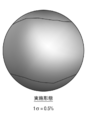
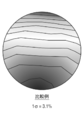
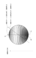
- FIG. 6A and 6B are explanatory diagrams showing the sheet resistance distribution (film thickness distribution) on the substrate 21.
- FIG. 6A shows the sheet resistance distribution (embodiment) on the substrate 21 when the sine wave control of the input power is performed.
- FIG. 6B shows a sheet resistance distribution (comparative example) when the input power is kept constant during film formation.
- the film formation conditions of the embodiment are as follows: the target material is NiFe, the film formation pressure is 0.05 Pa, the rotation speed of the substrate 21 is 60 rpm, the variation rate a of the input power amplitude A is 14%, and the center value B of the input power amplitude is B. 4 kW.
- the input power is constant at 4 kW, and other conditions are the same as in the embodiment.
- the in-plane distribution (1 ⁇ ) in the embodiment was 3.1%, whereas in the comparative example, it was 0.5%, and the uniformity of the in-plane distribution was extremely high in the embodiment. It was confirmed to be excellent.
- the magnetic field direction is a direction substantially orthogonal to the contour line, the sheet resistance is small on the N pole side (ie, the film thickness is large), and the sheet resistance value is large on the S pole side (ie, the film thickness is small). It has become.
- the contour lines indicate standardized sheet resistance values, and the interval is 0.01.
- the sheet resistance value Rn normalized here is expressed by the following formula (3).
- Rn Rs / Rs, max (3)
- Rs is a sheet resistance value
- Rs, max is a maximum value of the sheet resistance value.
- the input power control of the present embodiment is not limited to sine wave control, and control to switch the input power in two or more steps may be performed, or the input power is gradually increased as the first portion approaches the cathode. Can be reduced to the first power, and the input power can be gradually increased to the second power as the second portion approaches the cathode. Furthermore, a linear function or a quadratic function of the rotational position may be synthesized. Further, the same sine wave control may be performed during the film formation, but for example, the control method of the input power may be changed in the initial stage, the middle period, and the latter stage of the film formation. Further, in addition to the first part and the second part, the third part may be obtained and the input power different from that of the first part and the second part may be set.
- the rotation position of the substrate is not limited to a specific position, but includes a rotation interval (rotation position range) of the substrate having a range.
- the rotation position of the substrate is inserted in accordance with the rotation interval of the substrate.
- the average power level may be controlled.
- DC power having a predetermined magnitude or high-frequency power having a predetermined frequency may be intermittently supplied, and the input length or interval may be increased or decreased depending on the rotation interval of the substrate.
- control pattern may be changed according to the target material. This is because the tendency of the uneven distribution of film thickness varies depending on the target material.
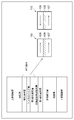
- FIG. 7 is a diagram showing only the controller 5 taken out, and the rest is the same as the configuration of FIG. 3 of the first embodiment.
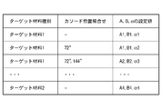
- the target material information acquisition unit 51c acquires target material information selected at the time of film formation as user input or data stored in advance.
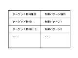
- the control pattern determination unit 51d holds a table as shown in FIG. 8, for example, and determines a control pattern based on the target material information acquired by the target material information acquisition unit 51c.
- FIG. 9 shows an example of the control pattern.
- FIG. 9 shows a film thickness distribution that can be obtained when a film is formed without using the method of the present invention.
- the direction in which the film thickness increases and the direction of the magnetic field coincide with each other.
- the phase ⁇ is set to 90 °.
- the fluctuation rate a and the like can be set to appropriate values according to the target material.
- FIG. 10 is a schematic cross-sectional view schematically showing the sputtering apparatus of the present embodiment, and shows a cross section taken along line ii of FIG.
- FIG. 11 is a plan view schematically showing the positional relationship between the substrate holder and the cathode unit.
- the same components as those in FIG. 1 of the first embodiment are denoted by the same reference numerals.
- a gas inlet 12 is opened in the chamber 10 of the sputtering apparatus 1 of the present embodiment, and a reactive processing gas (reactive gas) is introduced into the chamber 10 in the gas inlet 12.
- a reactive gas introduction system 13 to be introduced is connected.
- the reactive gas introduction system 13 is connected to a gas cylinder (not shown) via an automatic flow controller (not shown) such as a mass flow controller, for example, and the reactive gas is introduced from the gas inlet 12 at a predetermined flow rate.
- the reactive gas introduction system 12 supplies a reactive gas into the chamber 10 when reactive sputtering is performed in the chamber 10.
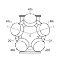
- a plurality of cathode units 40 each including a cathode for holding a target are disposed obliquely above the substrate holder 22 in the processing space. That is, a plurality of cathode units 40 are provided for one substrate holder 22, and each cathode unit 40 is attached to the upper wall portion of the chamber 10 in an inclined state.
- each cathode unit 40 is inclined with respect to the processing surface of the substrate 21 on the substrate holder 22 and is shifted from the central axis of the substrate 21 at an equal interval in the extending direction of the processing surface so as to be diagonally opposite the substrate 21.
- the cathode central axis of each cathode unit 40 is located away from the rotation axis of the substrate holder 22 and is arranged at equal intervals on a concentric circle spaced a predetermined distance from the rotation axis.
- the diameter of the substrate 21 and the target diameter are not particularly limited, but when the substrate 21 center and the cathode center are offset and the substrate 21 is rotated as in this embodiment, the target diameter is larger than the substrate 21 diameter. Even if it is small, uniform film formation is possible. Moreover, in this embodiment, since the five cathode units 40 are arrange
- each cathode unit 40 is electrically connected to a discharge power source (not shown) that applies a discharge voltage to the cathode.
- the discharge power may be any of high frequency power, DC power, and superposition of high frequency power and DC power.
- an individual discharge power source may be connected to each cathode unit 40, or switching such as a switch that selectively supplies power as a common power source. You may comprise so that a mechanism may be provided.
- a shutter 45 that selectively cuts off between a part of the cathodes and the substrate holder 22 is provided in front of each cathode unit 40. By selectively opening the shutter 45, a target can be selected from the plurality of cathode units 40 to perform sputtering, and contamination from other sputtered targets can be prevented. it can.
- FIG. 12 is a block diagram showing the configuration of the controller 5 and the cathode unit 40 in the present embodiment.
- the controller 5 shown in FIG. 12 calculates input power to each of the plurality of cathodes 41 so as to increase or decrease the film formation amount according to the rotational position detected by the position detector 23.
- a control signal (for example, a voltage or current corresponding to the calculated power value) is provided to correspond to each of the value calculator 51a and the plurality of cathodes 41 and adjust to the calculated power value.
- a control signal output unit 51b is provided to correspond to each of the value calculator 51a and the plurality of cathodes 41 and adjust to the calculated power value.
- the power control unit 52 of the cathode unit 40 increases or decreases the power of the discharge power supply 44 based on the control signal input from the control signal output unit 51b, and has a magnitude calculated by the input power value calculation unit 51a.
- Electric power is output to the cathode 41.
- the cathode 41 receives electric power for discharge corresponding to the rotational position of the substrate 21.
- the input power value can be, for example, a sine wave function of the rotation position of the substrate 21 as shown in FIG. 4, and the correspondence between the rotation position of the substrate 21 and the input power to the cathode 41 is shown in FIG.
- the input power value calculation unit 51a can calculate the input power value.
- a magnetic field is formed on the surfaces of the targets 42 of the plurality of cathode units 40, electric power for discharge is supplied, and plasma discharge is generated between the substrate holder 22 and the substrate.
- the operation of the sputtering apparatus according to this embodiment is the same as that described in the first embodiment (FIGS. 5 and 6) except that a plurality of targets are simultaneously sputtered. is there.
- the input power value calculation unit 51a of the controller 5 calculates for each cathode 41 using ⁇ as the angle formed by the specific position of the substrate and the installation position of each cathode 41 with respect to the rotation center, and the above equations (1), ( Applying 2), the input power value to each cathode is calculated.
- the magnetic field formed by the substrate-side magnet 30 rotates in synchronization with the substrate, so that even if the substrate is rotated, the uneven scattering amount of the sputtered particles cannot be eliminated.
- Difference in film thickness distribution When simultaneous sputtering is performed as in the present embodiment, the film thickness itself may be averaged depending on the positional relationship between the plurality of cathodes 41 that are simultaneously discharged.
- the target material also has a distribution bias as described above.
- the control pattern may be changed according to the target material. This is because the tendency of the uneven distribution of film thickness varies depending on the target material.
- FIG. 13 is a block diagram showing the configuration of the controller 5, and the rest is the same as the configuration of FIG. 4 of the first embodiment.
- the target material information acquisition unit 51c acquires target material information selected at the time of film formation as user input or data stored in advance.
- the cathode position acquisition unit 51f acquires the mutual positional relationship based on the combination of the plurality of cathodes 41 that are simultaneously discharged.
- the control pattern determination unit 51d holds a table as shown in FIG.
- control pattern is determined using a table as shown in FIG.
- FIG. 14 shows an example of determining the control pattern.
- the above formula A, B, and ⁇ in (1) are set to predetermined A1, B1, and ⁇ 1. Thereby, a film having a more uniform composition can be formed.
- the present invention can also be applied to high-frequency sputtering using a high-frequency power source. That is, the effect of improving the film thickness distribution can be obtained by controlling the high-frequency power so that the sputtering rate increases or decreases according to the rotational position of the substrate.
- the amplitude of high-frequency power serving as a base is changed according to the rotation position of the substrate, and the magnitude of average power per high-frequency cycle (or the magnitude of average power when the substrate is in a predetermined rotation section) is changed.
- the sputtering rate is changed according to the rotation position of the substrate.
- a high frequency power source for example, 1 MHz to 300 MHz
- a control signal is output from the control signal output unit 51b to the high frequency power source 55, and the high frequency power adjusted via the power adjustment unit 54 is supplied. It is also possible to supply to the cathode 41 via the matching circuit 53.
- the control signal is a signal whose amplitude is a sine wave function of the rotation position of the substrate, and high frequency power increased or decreased according to the rotation position of the substrate is input to the cathode.
- the central axis of the cathode 41 (target 42) in FIG. 1 is parallel to the central axis of the substrate 21 (substrate holder 22), but the central axis of the cathode 41 is in the direction in which the surface of the cathode 41 faces the substrate 21 side. It can also be inclined. Further, the prevention of film thickness unevenness between the first portion and the second portion increases the rotation speed of the substrate 21 when the first portion moves on the cathode 41 side, and the second portion becomes the cathode. It can also be performed by lowering the rotation speed of the substrate 21 when moving on the 41 side. Therefore, the generation of the film thickness distribution can be suppressed by using the control of the electric power for discharge and the control of the rotation speed of the substrate 21 in combination. For example, both the electric power for discharge and the rotation speed of the substrate 21 can be sine wave controlled.
- the cathode 41 is inclined with respect to the substrate holder 22, but as shown in FIG. 16, the central axis of the cathode 41 (target 42) is the center of the substrate 21 (substrate holder 22). You may arrange
- FIG. 17 is an explanatory diagram showing a TMR element as an example of an electronic component that can be formed by applying a sputtering method using the sputtering apparatus according to the present invention.
- the TMR element is a magnetic effect element (TMR (Tunneling Magnetoresistance) element).
- the basic layer configuration of the TMR element 110 includes a magnetic tunnel junction portion (MTJ portion) composed of the second magnetization fixed layer 107, the tunnel barrier layer 108, and the magnetization free layer 109.
- the second magnetization fixed layer 107 is made of a ferromagnetic material
- the tunnel barrier layer 108 is made of a metal oxide (magnesium oxide, alumina, etc.) insulating material
- the magnetization free layer 109 is made of a ferromagnetic material.
- the TMR element 110 applies an external magnetic field and applies the same voltage between the ferromagnetic layers on both sides of the tunnel barrier layer 108 and applies a constant current, and the magnetization directions of the ferromagnetic layers are the same in parallel. Sometimes (referred to as “parallel state”), the electrical resistance of the TMR element is minimized. Further, when the magnetization direction of the ferromagnetic layer is parallel and opposite (referred to as “anti-parallel state”), the electric resistance of the TMR element 110 has a maximum characteristic. Among these ferromagnetic layers on both sides, the second magnetization fixed layer 107 fixes the magnetization, and the magnetization free layer 109 is formed in a state in which the magnetization direction can be reversed by applying an external magnetic field for writing.
- the second magnetization fixed layer 107 In the film formation process of the second magnetization fixed layer 107, sputtering film formation is performed using the substrate-side magnet 30 in order to magnetize in a predetermined direction. At this time, the second magnetization fixed layer 107 having a uniform sheet resistance distribution can be formed by controlling the input power to be a sine wave in accordance with the rotational position of the substrate during film formation.
- the second magnetization fixed layer 107 for example, a material containing a ferromagnetic material such as Co, Fe, or Ni as a main component and appropriately adding a material such as B can be used.
- the substrate-side magnet 30 is used for magnetization in a predetermined direction when forming the first magnetization fixed layer, the magnetization free layer 109, and the like. Also in this case, by using the present invention, it is possible to form a film having excellent sheet resistance distribution uniformity.
Landscapes
- Chemical & Material Sciences (AREA)
- Engineering & Computer Science (AREA)
- Physics & Mathematics (AREA)
- Plasma & Fusion (AREA)
- Analytical Chemistry (AREA)
- Materials Engineering (AREA)
- Chemical Kinetics & Catalysis (AREA)
- Mechanical Engineering (AREA)
- Metallurgy (AREA)
- Organic Chemistry (AREA)
- Power Engineering (AREA)
- Nanotechnology (AREA)
- Manufacturing & Machinery (AREA)
- Crystallography & Structural Chemistry (AREA)
- Physical Vapour Deposition (AREA)
- Hall/Mr Elements (AREA)
- Thin Magnetic Films (AREA)
- Magnetic Heads (AREA)
Abstract
Priority Applications (6)
| Application Number | Priority Date | Filing Date | Title |
|---|---|---|---|
| JP2010522884A JP4739464B2 (ja) | 2008-12-26 | 2009-12-25 | スパッタリング装置、スパッタリング方法及び電子デバイスの製造方法 |
| CN200980147190.7A CN102227514B (zh) | 2008-12-26 | 2009-12-25 | 溅射装置、溅射方法和电子器件制造方法 |
| EP09834517.6A EP2390380B1 (fr) | 2008-12-26 | 2009-12-25 | Dispositif de pulvérisation, procédé de pulvérisation et procédé de fabrication de dispositif électronique |
| KR1020137002927A KR101271843B1 (ko) | 2008-12-26 | 2009-12-25 | 스퍼터링 장치, 스퍼터링 방법 및 전자 디바이스의 제조 방법 |
| KR1020117014654A KR101272009B1 (ko) | 2008-12-26 | 2009-12-25 | 스퍼터링 장치, 스퍼터링 방법 및 전자 디바이스의 제조 방법 |
| US13/104,472 US8906208B2 (en) | 2008-12-26 | 2011-05-10 | Sputtering apparatus, sputtering method, and electronic device manufacturing method |
Applications Claiming Priority (4)
| Application Number | Priority Date | Filing Date | Title |
|---|---|---|---|
| JP2008333066 | 2008-12-26 | ||
| JP2008-333480 | 2008-12-26 | ||
| JP2008-333066 | 2008-12-26 | ||
| JP2008333480 | 2008-12-26 |
Related Child Applications (1)
| Application Number | Title | Priority Date | Filing Date |
|---|---|---|---|
| US13/104,472 Continuation US8906208B2 (en) | 2008-12-26 | 2011-05-10 | Sputtering apparatus, sputtering method, and electronic device manufacturing method |
Publications (1)
| Publication Number | Publication Date |
|---|---|
| WO2010073711A1 true WO2010073711A1 (fr) | 2010-07-01 |
Family
ID=42287344
Family Applications (1)
| Application Number | Title | Priority Date | Filing Date |
|---|---|---|---|
| PCT/JP2009/007278 WO2010073711A1 (fr) | 2008-12-26 | 2009-12-25 | Dispositif de pulvérisation, procédé de pulvérisation et procédé de fabrication de dispositif électronique |
Country Status (6)
| Country | Link |
|---|---|
| US (1) | US8906208B2 (fr) |
| EP (1) | EP2390380B1 (fr) |
| JP (2) | JP4739464B2 (fr) |
| KR (2) | KR101271843B1 (fr) |
| CN (1) | CN102227514B (fr) |
| WO (1) | WO2010073711A1 (fr) |
Cited By (2)
| Publication number | Priority date | Publication date | Assignee | Title |
|---|---|---|---|---|
| WO2019111631A1 (fr) * | 2017-12-05 | 2019-06-13 | 昭和電工株式会社 | Procédé de fabrication d'un capteur magnétique, et ensemble capteur magnétique |
| JP2019201193A (ja) * | 2018-05-10 | 2019-11-21 | 株式会社アルバック | 抵抗体膜の製造方法及び抵抗体膜 |
Families Citing this family (21)
| Publication number | Priority date | Publication date | Assignee | Title |
|---|---|---|---|---|
| KR101332274B1 (ko) * | 2008-09-30 | 2013-11-22 | 캐논 아네르바 가부시키가이샤 | 스퍼터링 장치 및 스퍼터링 방법 |
| EP2390380B1 (fr) * | 2008-12-26 | 2016-03-09 | Canon Anelva Corporation | Dispositif de pulvérisation, procédé de pulvérisation et procédé de fabrication de dispositif électronique |
| KR20140104045A (ko) * | 2011-12-22 | 2014-08-27 | 캐논 아네르바 가부시키가이샤 | SrRuO3 막 증착 방법 |
| JP5806967B2 (ja) * | 2012-03-30 | 2015-11-10 | 株式会社クボタ | ディーゼルエンジンの排気処理装置 |
| CN103374705B (zh) * | 2012-04-11 | 2015-12-02 | 北京北方微电子基地设备工艺研究中心有限责任公司 | 一种磁控溅射装置 |
| US20130327634A1 (en) * | 2012-06-08 | 2013-12-12 | Chang-Beom Eom | Misaligned sputtering systems for the deposition of complex oxide thin films |
| WO2013189935A1 (fr) * | 2012-06-18 | 2013-12-27 | Oc Oerlikon Balzers Ag | Appareil pvd destiné au dépôt directionnel de matériau, procédés et pièce à usiner |
| JP2014046231A (ja) * | 2012-08-29 | 2014-03-17 | Hitachi Chemical Co Ltd | カーボンナノチューブ合成用触媒の製造方法 |
| KR101375878B1 (ko) * | 2012-09-27 | 2014-03-17 | 한국생산기술연구원 | 미세패턴 형성 방법 |
| KR101966029B1 (ko) * | 2013-07-11 | 2019-04-04 | 안드로이드 인더스트리즈 엘엘씨 | 밸런싱 디바이스, 균일성 디바이스 및 이들을 이용하기 위한 방법 |
| CN103487311B (zh) * | 2013-09-11 | 2016-04-13 | 广东省东莞市质量监督检测中心 | 一种湿浆样品置放装置及其控制方法 |
| US10196734B2 (en) * | 2014-03-25 | 2019-02-05 | Iowa State University Research Foundation, Inc. | Nanotwinned silver alloy film with controlled architecture |
| CN105112864B (zh) * | 2015-08-13 | 2019-03-05 | 江苏时代全芯存储科技有限公司 | 镀膜装置 |
| WO2017098537A1 (fr) * | 2015-12-07 | 2017-06-15 | キヤノンアネルバ株式会社 | Procédé et dispositif de fabrication d'élément à effet de magnétorésistance |
| US10431440B2 (en) * | 2015-12-20 | 2019-10-01 | Applied Materials, Inc. | Methods and apparatus for processing a substrate |
| DE102019200761A1 (de) * | 2019-01-22 | 2020-07-23 | TRUMPF Hüttinger GmbH + Co. KG | Verfahren zur Kompensation von Prozessschwankungen eines Plasmaprozesses und Regler für einen Leistungsgenerator zur Versorgung eines Plasmaprozesses |
| US11557473B2 (en) * | 2019-04-19 | 2023-01-17 | Applied Materials, Inc. | System and method to control PVD deposition uniformity |
| TW202104628A (zh) | 2019-04-19 | 2021-02-01 | 美商應用材料股份有限公司 | 用於控制pvd沉積均勻性的系統及方法 |
| WO2020257965A1 (fr) | 2019-06-24 | 2020-12-30 | Trumpf Huettinger (Shanghai) Co., Ltd. | Procédé de réglage de la puissance de sortie d'une alimentation électrique fournissant de l'énergie électrique à un plasma, appareil à plasma et alimentation électrique |
| KR20210006725A (ko) * | 2019-07-09 | 2021-01-19 | 삼성전자주식회사 | 스퍼터링 장치 및 이를 이용한 반도체 장치의 제조 방법 |
| CN110344013A (zh) * | 2019-08-19 | 2019-10-18 | 北京北方华创微电子装备有限公司 | 溅射方法 |
Citations (6)
| Publication number | Priority date | Publication date | Assignee | Title |
|---|---|---|---|---|
| JPS61250163A (ja) * | 1985-04-26 | 1986-11-07 | Nippon Telegr & Teleph Corp <Ntt> | 多層薄膜の製造方法および装置 |
| JPH06207270A (ja) * | 1993-01-07 | 1994-07-26 | Hitachi Ltd | 磁性膜形成装置 |
| JPH0969460A (ja) * | 1995-09-01 | 1997-03-11 | Kao Corp | 磁気記録媒体の製造方法 |
| JP2000265263A (ja) | 1999-01-12 | 2000-09-26 | Anelva Corp | スパッタリング方法及び装置 |
| JP2002069631A (ja) * | 2000-08-24 | 2002-03-08 | Hitachi Ltd | スパッタ方法及びその装置 |
| JP2002167661A (ja) * | 2000-11-30 | 2002-06-11 | Anelva Corp | 磁性多層膜作製装置 |
Family Cites Families (13)
| Publication number | Priority date | Publication date | Assignee | Title |
|---|---|---|---|---|
| JPS60207270A (ja) * | 1984-03-30 | 1985-10-18 | 日本航空電子工業株式会社 | コネクタ |
| US4607903A (en) | 1984-03-30 | 1986-08-26 | Japan Aviation Electronics Industry Limited | Connector assembly |
| US6290824B1 (en) | 1992-10-28 | 2001-09-18 | Hitachi, Ltd. | Magnetic film forming system |
| US6491802B2 (en) | 1992-10-28 | 2002-12-10 | Hitachi, Ltd. | Magnetic film forming system |
| JP4205294B2 (ja) * | 2000-08-01 | 2009-01-07 | キヤノンアネルバ株式会社 | 基板処理装置及び方法 |
| JP3505135B2 (ja) * | 2000-08-30 | 2004-03-08 | 株式会社日鉱マテリアルズ | 銅の表面処理方法 |
| WO2004036616A1 (fr) * | 2002-10-15 | 2004-04-29 | Unaxis Balzers Ag | Procede pour produire des substrats revetus par pulverisation cathodique magnetron et installation correspondante |
| US20050103620A1 (en) * | 2003-11-19 | 2005-05-19 | Zond, Inc. | Plasma source with segmented magnetron cathode |
| JP4494047B2 (ja) * | 2004-03-12 | 2010-06-30 | キヤノンアネルバ株式会社 | 多元スパッタ成膜装置の二重シャッタ制御方法 |
| JP4473323B2 (ja) * | 2007-04-26 | 2010-06-02 | キヤノンアネルバ株式会社 | スパッタリング成膜方法、電子デバイスの製造方法及びスパッタリング装置 |
| WO2009157341A1 (fr) | 2008-06-25 | 2009-12-30 | キヤノンアネルバ株式会社 | Dispositif de pulvérisation et support d'enregistrement sur lequel un programme de commande de celui-ci est enregistré |
| KR101332274B1 (ko) | 2008-09-30 | 2013-11-22 | 캐논 아네르바 가부시키가이샤 | 스퍼터링 장치 및 스퍼터링 방법 |
| EP2390380B1 (fr) * | 2008-12-26 | 2016-03-09 | Canon Anelva Corporation | Dispositif de pulvérisation, procédé de pulvérisation et procédé de fabrication de dispositif électronique |
-
2009
- 2009-12-25 EP EP09834517.6A patent/EP2390380B1/fr active Active
- 2009-12-25 JP JP2010522884A patent/JP4739464B2/ja active Active
- 2009-12-25 WO PCT/JP2009/007278 patent/WO2010073711A1/fr active Application Filing
- 2009-12-25 CN CN200980147190.7A patent/CN102227514B/zh active Active
- 2009-12-25 KR KR1020137002927A patent/KR101271843B1/ko active IP Right Grant
- 2009-12-25 KR KR1020117014654A patent/KR101272009B1/ko active IP Right Grant
-
2011
- 2011-04-25 JP JP2011097548A patent/JP5587822B2/ja active Active
- 2011-05-10 US US13/104,472 patent/US8906208B2/en active Active
Patent Citations (6)
| Publication number | Priority date | Publication date | Assignee | Title |
|---|---|---|---|---|
| JPS61250163A (ja) * | 1985-04-26 | 1986-11-07 | Nippon Telegr & Teleph Corp <Ntt> | 多層薄膜の製造方法および装置 |
| JPH06207270A (ja) * | 1993-01-07 | 1994-07-26 | Hitachi Ltd | 磁性膜形成装置 |
| JPH0969460A (ja) * | 1995-09-01 | 1997-03-11 | Kao Corp | 磁気記録媒体の製造方法 |
| JP2000265263A (ja) | 1999-01-12 | 2000-09-26 | Anelva Corp | スパッタリング方法及び装置 |
| JP2002069631A (ja) * | 2000-08-24 | 2002-03-08 | Hitachi Ltd | スパッタ方法及びその装置 |
| JP2002167661A (ja) * | 2000-11-30 | 2002-06-11 | Anelva Corp | 磁性多層膜作製装置 |
Non-Patent Citations (1)
| Title |
|---|
| See also references of EP2390380A4 |
Cited By (4)
| Publication number | Priority date | Publication date | Assignee | Title |
|---|---|---|---|---|
| WO2019111631A1 (fr) * | 2017-12-05 | 2019-06-13 | 昭和電工株式会社 | Procédé de fabrication d'un capteur magnétique, et ensemble capteur magnétique |
| JP2019102681A (ja) * | 2017-12-05 | 2019-06-24 | 昭和電工株式会社 | 磁気センサの製造方法及び磁気センサ集合体 |
| JP2019201193A (ja) * | 2018-05-10 | 2019-11-21 | 株式会社アルバック | 抵抗体膜の製造方法及び抵抗体膜 |
| JP7120857B2 (ja) | 2018-05-10 | 2022-08-17 | 株式会社アルバック | 抵抗体膜の製造方法及び抵抗体膜 |
Also Published As
| Publication number | Publication date |
|---|---|
| EP2390380A1 (fr) | 2011-11-30 |
| JP5587822B2 (ja) | 2014-09-10 |
| US20110209986A1 (en) | 2011-09-01 |
| EP2390380A4 (fr) | 2014-01-08 |
| KR101272009B1 (ko) | 2013-06-05 |
| JP2011149104A (ja) | 2011-08-04 |
| JPWO2010073711A1 (ja) | 2012-06-14 |
| KR20110089878A (ko) | 2011-08-09 |
| EP2390380B1 (fr) | 2016-03-09 |
| KR101271843B1 (ko) | 2013-06-07 |
| KR20130019035A (ko) | 2013-02-25 |
| JP4739464B2 (ja) | 2011-08-03 |
| US8906208B2 (en) | 2014-12-09 |
| CN102227514B (zh) | 2014-08-20 |
| CN102227514A (zh) | 2011-10-26 |
Similar Documents
| Publication | Publication Date | Title |
|---|---|---|
| JP4739464B2 (ja) | スパッタリング装置、スパッタリング方法及び電子デバイスの製造方法 | |
| JP5192549B2 (ja) | スパッタリング装置及びスパッタリング方法 | |
| US10636634B2 (en) | Sputtering apparatus, film deposition method, and control device | |
| JP4727764B2 (ja) | プラズマ処理装置、磁気抵抗素子の製造装置、磁性薄膜の成膜方法及び成膜制御プログラム | |
| US7955480B2 (en) | Sputtering apparatus and film deposition method | |
| US20130048494A1 (en) | Sputtering device | |
| EP1994196A1 (fr) | Systeme de deposition par pulverisation cathodique et ses procedes d'utilisation | |
| CN110177898A (zh) | 溅射装置及成膜方法 | |
| JP2006233240A (ja) | スパッタ用カソード及びスパッタ装置 | |
| JP4974582B2 (ja) | 成膜装置 |
Legal Events
| Date | Code | Title | Description |
|---|---|---|---|
| WWE | Wipo information: entry into national phase |
Ref document number: 200980147190.7 Country of ref document: CN |
|
| WWE | Wipo information: entry into national phase |
Ref document number: 2010522884 Country of ref document: JP |
|
| 121 | Ep: the epo has been informed by wipo that ep was designated in this application |
Ref document number: 09834517 Country of ref document: EP Kind code of ref document: A1 |
|
| WWE | Wipo information: entry into national phase |
Ref document number: 2009834517 Country of ref document: EP |
|
| ENP | Entry into the national phase |
Ref document number: 20117014654 Country of ref document: KR Kind code of ref document: A |
|
| NENP | Non-entry into the national phase |
Ref country code: DE |