WO2010073487A1 - 保持部材管理装置、半導体製造装置、保持部材管理方法、及び、半導体装置の製造方法 - Google Patents
保持部材管理装置、半導体製造装置、保持部材管理方法、及び、半導体装置の製造方法 Download PDFInfo
- Publication number
- WO2010073487A1 WO2010073487A1 PCT/JP2009/006428 JP2009006428W WO2010073487A1 WO 2010073487 A1 WO2010073487 A1 WO 2010073487A1 JP 2009006428 W JP2009006428 W JP 2009006428W WO 2010073487 A1 WO2010073487 A1 WO 2010073487A1
- Authority
- WO
- WIPO (PCT)
- Prior art keywords
- holding member
- yield
- identification information
- member management
- unit
- Prior art date
- Legal status (The legal status is an assumption and is not a legal conclusion. Google has not performed a legal analysis and makes no representation as to the accuracy of the status listed.)
- Ceased
Links
Images




Classifications
-
- H—ELECTRICITY
- H10—SEMICONDUCTOR DEVICES; ELECTRIC SOLID-STATE DEVICES NOT OTHERWISE PROVIDED FOR
- H10P—GENERIC PROCESSES OR APPARATUS FOR THE MANUFACTURE OR TREATMENT OF DEVICES COVERED BY CLASS H10
- H10P72/00—Handling or holding of wafers, substrates or devices during manufacture or treatment thereof
- H10P72/04—Apparatus for manufacture or treatment
- H10P72/0428—Apparatus for mechanical treatment or grinding or cutting
-
- H—ELECTRICITY
- H10—SEMICONDUCTOR DEVICES; ELECTRIC SOLID-STATE DEVICES NOT OTHERWISE PROVIDED FOR
- H10P—GENERIC PROCESSES OR APPARATUS FOR THE MANUFACTURE OR TREATMENT OF DEVICES COVERED BY CLASS H10
- H10P72/00—Handling or holding of wafers, substrates or devices during manufacture or treatment thereof
- H10P72/06—Apparatus for monitoring, sorting, marking, testing or measuring
- H10P72/0604—Process monitoring, e.g. flow or thickness monitoring
Definitions
- the present invention relates to a holding member management apparatus, a semiconductor manufacturing apparatus, a holding member management method, and a semiconductor device manufacturing method.
- a bonding apparatus that bonds a plurality of wafers by pressurizing and heating a pair of wafer holders sandwiching the plurality of wafers is known (for example, see Patent Document 1).
- the wafer bonding yield is lowered by continuing the use of the wafer holder whose characteristics such as flatness do not reach an allowable level.
- a holding member management apparatus that manages a holding member that holds a substrate in order to process the substrate, wherein the substrate is held by the holding member.
- An acquisition unit that acquires inspection information about the quality of processing
- a calculation unit that calculates a yield after processing of the substrate held by the holding member based on the inspection information acquired by the acquisition unit
- a holding member management device is provided that includes a determination unit that determines the quality of the holding member based on the yield calculated by the calculation unit.
- a holding member management apparatus that manages a plurality of holding members that hold a plurality of substrates in order to process the plurality of substrates, and each of the plurality of holding members is identified.
- An acquisition unit that acquires identification information and inspection information about the quality of processing of the substrate held by the holding member identified by the identification information, and the identification information and the inspection information acquired by the acquisition unit
- a calculation unit that calculates a yield after processing of the substrate held by the holding member that is identified by the identification information corresponding to the inspection information, and the plurality based on the yield calculated by the calculation unit
- a holding member management device is provided that includes a determination unit that determines the quality of each of the holding members.
- the holding member management device, a bonding device for bonding a plurality of substrates, and a semiconductor substrate bonded by the bonding device are inspected for quality, and the inspection result is managed by the holding member management.
- a semiconductor manufacturing apparatus including an inspection apparatus that outputs to the acquisition unit of the apparatus.
- a holding member management method for managing a holding member that holds a substrate in order to process the substrate, and whether or not the substrate held by the holding member is bonded.
- An acquisition step for acquiring inspection information, and a calculation step for calculating a yield after processing of the substrate held by the holding member corresponding to the inspection information based on the inspection information acquired in the acquisition step;
- a holding member management method comprising: a determination step of determining pass / fail of the holding member based on the yield calculated in the calculating step.
- a holding member management method for managing a plurality of holding members for holding a plurality of substrates in order to process a plurality of substrates, respectively identifying each of the plurality of holding members.
- Acquisition step for acquiring identification information to be performed, and inspection information on the quality of processing of the substrate held by the holding member identified by the identification information, and the identification information acquired in the acquisition step and the inspection
- a calculation step of calculating a yield after processing of the substrate held by the holding member identified by the identification information corresponding to the inspection information, and the yield calculated in the calculation step based on the yield
- a determination step of determining whether each of the plurality of holding members is acceptable.
- the step of managing the holding member by the holding member management device the step of bonding the semiconductor substrate by the bonding device for bonding a plurality of semiconductor substrates using the holding member, and the semiconductor bonded by the bonding device And a step of inspecting the quality of the substrate using an inspection device and outputting the inspection result to the acquisition unit of the holding member management device.
- FIG. 1 is a plan view schematically showing a semiconductor manufacturing apparatus 10.
- 2 is a plan view schematically showing a wafer W.
- FIG. It is sectional drawing which shows typically the structure of alignment mechanism 12 single. It is a figure which shows operation
- 3 is a side sectional view showing a schematic configuration of a joining mechanism 14.
- FIG. 2 is a block diagram showing a schematic configuration of a holding member management apparatus 100.
- FIG. 4 is a flowchart for explaining a wafer W inspection method. It is a flowchart for demonstrating the management method of the wafer holder WH. It is a flowchart for demonstrating the management method of the wafer holder WH which concerns on another Example.
- FIG. 1 is a plan view schematically showing a semiconductor manufacturing apparatus 10 including a holding member management apparatus 100.
- the semiconductor manufacturing apparatus 10 includes an alignment mechanism 12 that aligns the relative positions of two wafers W, and a bonding mechanism 14 that bonds a pair of wafers W aligned by the alignment mechanism 12.
- each wafer W before being aligned is held by the wafer holder WH with a suction force such as electrostatic attraction, and the aligned pair of wafers W is held between the pair of wafer holders WH.
- the semiconductor manufacturing apparatus 10 includes a transport mechanism 16 that transports the pair of wafers W from the alignment mechanism 12 to the bonding mechanism 14 together with the pair of wafer holders WH that hold the wafers W.
- the pair of wafers W are bonded together in the bonding mechanism 14 by being pressurized and heated together with the wafer holder WH.
- the semiconductor manufacturing apparatus 10 includes a semiconductor inspection apparatus 101.
- the semiconductor inspection apparatus 101 includes a pre-bonding inspection apparatus 102 that inspects the wafer W before being aligned by the alignment mechanism 12, and a post-bonding inspection apparatus 104 that inspects the wafer W bonded by the bonding mechanism 14. I have. Further, the semiconductor inspection apparatus 101 temporarily receives the inspection results of the CPU 105 as an analysis unit that analyzes the inspection results of the pre-bonding inspection apparatus 102 and the post-bonding inspection apparatus 104, and the pre-bonding inspection apparatus 102 and the post-bonding inspection apparatus 104. And a memory 107 serving as a storage unit.
- the semiconductor manufacturing apparatus 10 includes bar code readers 106 and 108 as identification information reading units that read bar codes as identification displays attached to the wafer W and the wafer holder WH.
- the barcode reader 106 is arranged in the pre-bonding inspection apparatus 102 and reads the wafer W before being aligned by the alignment mechanism 12 and the barcode attached to the wafer holder WH that holds the wafer W.
- the barcode reader 108 is arranged in the post-bonding inspection apparatus 104 and reads a barcode attached to the wafer W after being bonded by the bonding mechanism 14.
- the pre-bonding inspection apparatus 102 performs various inspections on the wafer W before bonding.
- the pre-bonding inspection apparatus 102 performs transistor switching voltage, electrode resistance measurement, continuity test, and the like for all dies formed on the wafer W.
- a so-called probe test using an inspection needle can be used for the inspection by the inspection apparatus 102 before bonding and the inspection apparatus 104 after bonding.
- the post-bonding inspection apparatus 104 performs various inspections on the wafer W after bonding. For example, the post-bonding inspection apparatus 104 performs transistor switching voltage, electrode resistance value, fringe capacitance measurement between bonded electrodes, continuity test, and the like for all dies formed on the wafer W.
- the CPU 105 calculates the fluctuation amount of the measurement result before and after bonding for all the dies formed on the wafer W, and determines whether or not the fluctuation amount is equal to or less than a threshold value.
- the CPU 105 determines that each die is good when the variation amount is equal to or less than the threshold value and when it is determined good in the continuity test.
- the CPU 105 determines that each die is defective when the amount of fluctuation exceeds a threshold value and when it is determined as defective in the continuity test. Then, the CPU 105 calculates the number of dies determined to be good.
- the CPU 105 reads the barcode information of the wafer holder WH read by the barcode readers 106 and 108, the number of die inspections and the number of good judgment dies for the wafer W held by the wafer holder WH identified by the barcode information. To the holding member management apparatus 100 in association with each other. The holding member management apparatus 100 manages the barcode information and the number of die inspections and the number of good dies for the wafer holder WH identified by the barcode information in association with each other.
- FIG. 2 is a plan view schematically showing the wafer W.
- a wafer W includes transistors and resistors (not shown) in a plurality of dies D partitioned in a matrix on one surface of a circular thin plate member B formed of single crystal silicon as a semiconductor material.
- circuit elements such as a capacitor, are formed.
- the circuit element is formed by using a forming technique such as a thin film forming technique, an etching technique, and an impurity diffusion technique with a lithography technique as a core.
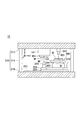
- FIG. 3 is a cross-sectional view schematically showing the structure of the alignment mechanism 12 alone.
- the alignment mechanism 12 includes a fixed stage 141, a moving stage 142, and an elevating / lowering unit 360 disposed inside the frame 310.
- the frame 310 includes a top plate 312 and a bottom plate 316 that are parallel to each other and a plurality of support columns 314 that couple the top plate 312 and the bottom plate 316 together.
- the top plate 312, the support column 314, and the bottom plate 316 are each formed of a highly rigid material and do not deform even when a reaction force relating to the operation of the internal mechanism is applied.
- the fixed stage 141 is fixed to the lower surface of the top plate 312 and holds the wafer W held by the wafer holder WH on the lower surface.
- the wafer W is held on the lower surface of the wafer holder WH by electrostatic attraction and becomes one of alignment targets described later.
- the moving stage 142 is placed on the bottom plate 316 and moved in the X direction while being guided by a guide rail 352 fixed to the bottom plate, and the Y stage moves on the X stage 354 in the Y direction.
- a stage 356 Thereby, the member mounted on the moving stage 142 can be moved in any direction on the XY plane.
- the elevating unit 360 is mounted on the moving stage 142 and includes a cylinder 362 and a piston 364.
- the piston 364 moves up and down in the Z direction in the cylinder 362 in response to an instruction from the outside.
- a wafer holder WH is held on the upper surface of the piston 364. Further, the wafer W is held on the wafer holder WH.
- the wafer W is one of alignment targets to be described later.
- the wafer W has an alignment mark M serving as an alignment reference on the surface (the lower surface in the drawing).
- the alignment mark M is not necessarily a graphic or the like provided for that purpose, but may be a wiring, a bump, a scribe line, or the like formed on the wafer W.
- the alignment mechanism 12 further includes a pair of microscopes 342 and 344 and a reflecting mirror 372.
- One microscope 342 is fixed to the lower surface of the top plate 312 with a predetermined interval with respect to the fixed stage 141.
- the other microscope 344 and reflecting mirror 372 are mounted on the moving stage 142 together with the elevating unit 360. Thereby, the microscope 344 and the reflecting mirror 372 move on the XY plane together with the lifting unit 360.
- the microscope 344 and the reflecting mirror 372 and the elevating unit 360 have a known distance.
- the alignment mechanism 12 When the alignment mechanism 12 is in the state shown in the figure, the alignment marks M of the opposing wafers W and 182 can be observed using the microscopes 342 and 344. Therefore, for example, the exact position of the wafer W can be known from the image obtained by the microscope 342. Further, the exact position of the wafer W can be known from the image obtained by the microscope 344.
- the reflecting mirror 372 is used when the moving amount of the moving stage 142 is measured using a measuring device such as an interferometer.
- a measuring device such as an interferometer.
- FIG. 1 a reflecting mirror 372 arranged at right angles to the paper surface is shown, but another reflecting mirror 372 for detecting movement in the Y direction is also provided.
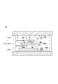
- FIG. 4 is a diagram illustrating the operation of the alignment mechanism 12.
- the moving stage 142 is moved in the X direction.
- the wafer W on the moving stage 142 is moved to the fixed stage 141. It is transported directly below.
- the alignment marks M of the upper and lower wafers W are located on one vertical line.
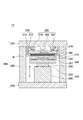
- FIG. 5 is a side sectional view showing a schematic configuration of the joining mechanism 14.
- the joining mechanism 14 includes a pressing part 246, a pressure stage 248, a pressure receiving stage 250, and a pressure detection part 252 arranged inside the frame body 244.
- the frame 244 includes a top plate 254 and a bottom plate 256 that are parallel and parallel to each other, and a plurality of support columns 258 that couple the top plate 254 and the bottom plate 256 together.
- the top plate 254, the support column 258, and the bottom plate 256 have such rigidity that no deformation occurs when a reaction force of pressure applied to the wafer W and the wafer holder WH is applied.
- the pressing part 246 is disposed on the bottom plate 256 inside the frame body 244.
- the pressing unit 246 includes a cylinder 260 fixed to the upper surface of the bottom plate 256 and a piston 262 disposed inside the cylinder 260.
- the piston 262 is driven by a fluid circuit (not shown), a cam, a train wheel, and the like, and moves up and down in a direction perpendicular to the bottom plate 256 indicated by an arrow Z in the drawing.
- a pressure stage 248 is mounted on the upper end of the piston 262.
- the pressure stage 248 includes a horizontal plate-like support portion 266 coupled to the upper end of the piston 262 and a plate-like first substrate holding portion 268 parallel to the support portion 266.
- the first substrate holding unit 268 is supported from the support unit 266 via a plurality of actuators 267.
- the actuator 267 is also arranged forward and backward with respect to the paper surface.
- Each of these actuators 267 can be operated independently of each other. With such a structure, the inclination of the first substrate holding portion 268 can be arbitrarily changed by appropriately operating the actuator 267.
- the first substrate holding unit 268 includes a heater 270 and is heated by the heater 270.
- the wafer W is electrostatically attracted to the wafer holder WH, and the first substrate holder 268 attracts the wafer holder WH to the upper surface by vacuum suction or the like. As a result, the wafer W swings together with the wafer holder WH and the first substrate holder 268, while being prevented from moving or dropping from the first substrate holder 268.
- the pressure receiving stage 250 includes a second substrate holding part 272 and a plurality of suspension parts 274.
- the suspension portion 274 is suspended from the lower surface of the top plate 254.
- the second substrate holding part 272 is supported from below in the vicinity of the lower end of the suspension part 274 and is disposed to face the pressure stage 248.
- the second substrate holding unit 272 sucks the wafer holder WH on the lower surface by vacuum suction or the like. Further, the second substrate holding unit 272 includes a heater 276 and is heated by the heater 276.
- the second substrate holding part 272 is supported by the suspension part 274 from below, but its upward movement is not restricted. However, a plurality of load cells 278, 280, 282 are sandwiched between the top plate 254 and the second substrate holding part 272. The plurality of load cells 278, 280, and 282 form part of the pressure detection unit 252 to restrict the upward movement of the second substrate holding unit 272 and are applied upward to the second substrate holding unit 272. Detect pressure.
- the pressure stage 248 moves up toward the pressure receiving stage 250 and presses the pair of wafers W. Further, the heaters 270 and 276 heat the pressure stage 248 and the pressure receiving stage 250 during pressing. Thereby, a pair of wafers W are joined.
- FIG. 6 is a block diagram illustrating a schematic configuration of the holding member management apparatus 100.
- the holding member management apparatus 100 includes a control unit 110 that controls the entire holding member management apparatus 100, an interface unit 112 as an acquisition unit, and a notification unit 114.
- the interface unit 112 transmits information acquired from the barcode readers 106 and 108 and the CPU 105 of the semiconductor inspection apparatus 101 to the control unit 110.
- the notification unit 114 notifies the user of various types of information such as warnings (warnings).
- the control unit 110 includes a calculation unit, a determination unit, an output unit, a CPU 116 as an extraction unit, and a memory 118 as a storage unit.
- the memory 118 stores the barcode information of the wafer holder WH, the number of inspections of the die D and the number of good dies D for the wafer W held by the wafer holder WH identified by the barcode information.
- the number of inspections of the dies D and the number of good dies D are accumulated for each corresponding barcode information.
- the CPU 116 calculates the ratio of the integrated value of the good judgment die D stored in the memory 118 to the integrated value of the number of inspections of the die D, that is, the yield for each corresponding barcode information. Then, the CPU 116 determines whether or not the calculated yield is equal to or less than a threshold for determining whether or not to continue using the wafer holder WH.
- CPU105 outputs barcode information to the notification part 114, when the said yield exceeds a threshold value.
- the notification unit 114 notifies the user of the received barcode information.
- the threshold for determining whether or not to continue using the wafer holder WH is set by the difference from the average yield. Alternatively, the threshold value is set to a predetermined value.
- FIG. 7 is a flowchart for explaining the wafer W inspection method.
- the processing routine is started, and the process proceeds to step S100.
- the barcode reader 106 reads the barcode information of the wafer W and the wafer holder WH and outputs it to the memory 107.
- the pre-bonding inspection apparatus 102 performs the above-described inspection on the wafer W before bonding and outputs the inspection result to the memory 107.
- the process proceeds to step S104.
- the memory 107 stores the barcode information of the wafer W and wafer holder WH input in step S100 and the inspection result input in step S102 in association with each other.
- step S106 the bonded wafer W is transferred to the post-bonding inspection apparatus 104, and the barcode reader 108 reads the barcode information of the wafer W and outputs it to the memory 107.
- step S ⁇ b> 108 the post-bonding inspection apparatus 104 performs the above-described inspection on the bonded wafer W and outputs the inspection result to the memory 107.
- step S110 the memory 107 stores the barcode information of the wafer W and wafer holder WH input in step S106 and the inspection result input in step S108 in association with each other.
- step S112 the CPU 105 reads the barcode information input in step S106 and the inspection results before and after joining corresponding to the barcode information from the memory 107. Then, based on the read inspection results before and after bonding, the amount of variation in various measured values such as transistor switching voltage and electrode resistance in each die D of the wafer W before and after bonding, and the fringe capacity between the bonded electrodes Then, it is determined whether or not the calculated value is equal to or greater than a threshold value. If the determination is affirmative, the process proceeds to step S114, whereas if the determination is negative, the processing routine is terminated.
- step S114 the CPU 105 determines pass / fail of the continuity test for each die D of the wafer W after bonding. If the determination is affirmative, each die D is determined to be good and the process proceeds to step S116. If the determination is negative, the processing routine is terminated.
- step S116 the CPU 105 calculates the number of dies D determined to be good, and in step S104 and step S110, the calculation result is displayed together with the barcode information associated with the inspection result. To 100 control units 110. Thus, the present processing routine ends.
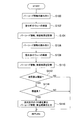
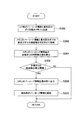
- FIG. 8 is a flowchart for explaining a method for managing the wafer holder WH.
- the processing routine shown in the flowchart is started when the semiconductor manufacturing apparatus 10 starts the alignment adjustment and bonding operations of the wafer W, and proceeds to step S200.
- the interface unit 112 transmits the barcode information of the wafer holder WH output from the CPU 105 of the semiconductor inspection apparatus 101 in step S114 and the number of good dies D to the memory 118. Then, the process proceeds to step S202.
- step S202 the memory 118 stores the input barcode information in association with the number of good dies D and the number of inspections of the dies D.
- the stored number of good judgment dies D and the number of inspections of the dies D are added to the already stored values.
- step S ⁇ b> 204 the CPU 116 calculates a yield, which is a ratio of the integrated value of the good judgment die D stored in the memory 118 to the integrated value of the number of inspections of the die D for each corresponding barcode information. Then, the process proceeds to step S206.
- step S206 the CPU 116 determines whether or not the calculated yield is equal to or less than a threshold value for determining whether or not to continue using the wafer holder WH. If the determination is affirmative, the process proceeds to step S208. If the determination is negative, the processing routine ends.
- step S208 the CPU 116 outputs the barcode information to the notification unit 114.
- step S210 the notification unit 114 notifies the user of the received barcode information. Thus, the processing routine is finished.
- the quality of the bonding of the wafer W is determined depending on the flatness of the wafer holder WH, that is, the quality of the wafer holder WH. For this reason, it is appropriate to find a wafer holder WH with reduced quality and stop using the wafer holder WH.
- the yield of the wafer W bonded using the wafer holder WH is obtained, and the obtained yield is compared with a threshold value to find a wafer holder WH having a lowered quality. . Then, the user is notified that the use of the found wafer holder WH should be stopped.
- management of the wafer holder WH can be automated by associating the wafer holder WH and the barcode information attached to the wafer W with the inspection result. Man-hours can be reduced. Further, in the present embodiment, the holding member management apparatus 100 and the semiconductor inspection apparatus 101 can inspect the wafer holder WH by inspecting the wafer W and associating the inspection result with the wafer holder WH. Inspection man-hours can be reduced.
- the notification unit 114 performs a process of notifying the user of the barcode information of the wafer holder WH.
- the CPU 116 outputs a signal for stopping the use of the wafer holder WH to the alignment mechanism 12 and the bonding mechanism 14, and performs a process of stopping the use of the wafer holder WH in the alignment mechanism 12 and the bonding mechanism 14. Also good.
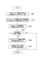
- FIG. 9 is a flowchart for explaining a method for managing the wafer holder WH according to another embodiment.
- the processing routine shown in the flowchart is started when the semiconductor manufacturing apparatus 10 starts operations for alignment adjustment and bonding of the wafer W, and proceeds to step S300.
- the interface unit 112 transmits the barcode information of the wafer holder WH output from the CPU 105 of the semiconductor inspection apparatus 101 in step S114 and information on the number of good dies D to the memory 118. Then, the process proceeds to step S302.
- step S302 the memory 118 stores the input barcode information in association with the information on the number of dies D and the number of inspections of the dies D that are determined to be good.
- step S304 the CPU 116 calculates a yield, which is a ratio of the number of good judgment dies D stored in the memory 118 to the number of inspections of the dies D, for each corresponding barcode information.
- the CPU 116 outputs the calculation result to the memory 118 together with the barcode information, and the memory 118 stores the input calculation result and the barcode information in association with each other.
- the CPU 116 calculates the amount of change between the yield calculated in this step and the yield stored in the memory 118 a predetermined time ago, that is, the time differential value of the yield, which is the amount of change in yield per fixed time.
- step S306 the CPU 116 determines whether or not the time differential value of the bonding yield is equal to or less than a threshold for determining whether or not to continue using the wafer holder WH. If the determination is affirmative, the process proceeds to step S308. If the determination is negative, the processing routine ends.
- step S308 the CPU 116 outputs the barcode information to the notification unit 114.
- step S310 the notification unit 114 notifies the user of the received barcode information. Thus, the processing routine is finished.
- the ratio of the yield of the wafers W bonded using the wafer holder WH is reduced per fixed time, and the obtained value is compared with a threshold value. Discovering a lowered wafer holder WH. Then, the user is notified that the use of the found wafer holder WH should be stopped. As a result, the use of the wafer holder WH whose quality is reduced can be continued, and the reduction in the bonding yield of the wafer W can be suppressed from increasing.
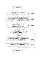
- FIG. 10 is a flowchart for explaining a method for managing the wafer holder WH according to another embodiment.
- the semiconductor manufacturing apparatus 10 is started when the wafer W alignment adjustment and bonding operations are started, and the process proceeds to step S400.
- the interface unit 112 transmits the barcode information of the wafer holder WH and the information on the number of good dies D output from the CPU 105 of the semiconductor inspection apparatus 101 in step S114 to the memory 118. Then, the process proceeds to step S402.
- step S ⁇ b> 114 the number of good dies D for each region (for example, the first quadrant to the fourth quadrant) obtained by dividing the wafer W into a plurality of parts is output from the CPU 105 to the memory 118 via the interface unit 112.
- step S402 the memory 118 stores the input barcode information in association with the information on the number of good dies D and the number of inspections of the dies D for each region. The stored number of good judgment dies D and the number of inspections of the dies D are added to the already stored values.
- step S ⁇ b> 404 the CPU 116 calculates the yield for each barcode information and each area stored in the memory 118. Then, the process proceeds to step S406.
- step S406 the CPU 116 determines whether or not the yield for each area is equal to or less than a threshold for determining whether or not to continue using the wafer holder WH. If the determination is affirmative, the process proceeds to step S408. If the determination is negative, the processing routine is terminated.
- step S408 the CPU 116 outputs the barcode information and information designating the area to the notification unit 114.
- step S410 the notification unit 114 notifies the user of the received barcode information and information specifying the area. Thus, the processing routine is finished.
- the yield of each divided region in the wafer W bonded using the wafer holder WH is obtained, and the obtained value is compared with a threshold value, thereby reducing the quality.
- the wafer holder WH and the area where the quality of the wafer holder WH is degraded are found. Then, the user is notified of the fact that the use of the found wafer holder WH should be stopped and the area of the wafer holder WH to be repaired and cleaned.
- the use of the wafer holder WH having a deteriorated quality can be continued, and a reduction in the bonding yield of the wafer W can be suppressed. Further, since the user can know the area to be repaired and cleaned in the wafer holder WH, it is possible to efficiently perform the repair and cleaning of the wafer holder WH.
- the yield of each region corresponding to the four regions from the first quadrant to the fourth quadrant of the wafer W among the regions of the wafer holder WH has been calculated. Instead, the yield of each region corresponding to each die D of the wafer W among the regions of the wafer holder WH can be calculated. As a result, it is possible to identify an area where the defective chip is formed, that is, an area where the quality is deteriorated, among the areas of the wafer holder WH.
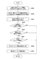
- FIG. 11 is a flowchart for explaining a method for managing the wafer holder WH according to another embodiment.
- the semiconductor manufacturing apparatus 10 starts when the wafer W alignment adjustment and bonding operations are started, and the process proceeds to step S500.
- step S500 the interface unit 112 transmits the barcode information of the wafer holder WH output from the CPU 105 of the semiconductor inspection apparatus 101 in step S114 and information on the number of good dies D to the memory 118. Then, the process proceeds to step S502.
- step S114 a set of barcode information for identifying a set of wafer holders WH used in combination and an inspection result of the wafer W bonded using the set of wafer holders WH are output. .
- step S502 the memory 118 stores the input set of bar code information in association with the number of good Dies D and the number of inspections of the Dies D. The stored number of good judgment dies D and the number of inspections of the dies D are added to the already stored values.
- step S ⁇ b> 504 the CPU 116 calculates the yield of the wafer W for each set of barcode information stored in the memory 118. For example, ID No. 3 wafer holder WH and IDNo. 7 in combination with the wafer holder WH of No. 7, the yield of the wafer W is 95%. 4 wafer holder WH and IDNo. The yield of the wafer W in the combination with the eight wafer holders WH is calculated as 92%. Then, the process proceeds to step S506.
- step S506 the CPU 116 determines whether there is a calculated yield for each set that is equal to or less than a threshold value. If the determination is affirmative, the process proceeds to step S508. If the determination is negative, the processing routine is terminated.
- step S508 the CPU 116 circulates the plurality of wafer holders WH so that the combination of the wafer holders WH in each group does not become a combination in which the yield is less than or equal to the threshold value.
- the wafer holder WH of the combination is transported with a phase shift.
- the transfer of one wafer holder WH is stopped and the other wafer holder WH is transferred to the pre-bonding inspection apparatus 102.
- the combination of the wafer holders WH is determined so as not to be the combination. Thereby, it is possible to suppress a decrease in the bonding yield of the wafer W without stopping the use of the wafer holder WH.
- the CPU 116 uniformizes the probability of the combination of each set by changing the combination of each set of the wafer holders WH with a certain regularity. Thereby, the inspection results of the wafers W for all combinations can be acquired, and the total number of inspections of the wafers W for each combination, that is, the population can be averaged. Therefore, the reliability of the data to be compared when comparing the calculation results of the yield of the wafer W for each combination can be improved, and thus the accuracy in finding an inappropriate combination of the wafer holders W can be improved.
- a method of changing the combination of wafer holders WH a method of changing randomly may be used.
- FIG. 12 is a flowchart for explaining a method for managing the wafer holder WH according to another embodiment.
- the above-described steps S500 to S506 are performed when the semiconductor manufacturing apparatus 10 starts the alignment adjustment and bonding operations of the wafer W, and the process proceeds to step S600.
- step S600 the CPU 116 determines whether or not there are a plurality of combinations of bar code information whose yield is equal to or less than a threshold value. If the determination is affirmative, the process proceeds to step S602. If the determination is negative, the processing routine ends.
- step S602 the CPU 116 determines whether there is barcode information included in any of a plurality of sets of barcode information whose yield is equal to or less than a threshold value.
- a threshold value For example, ID No. 2 wafer holder WH and IDNo. No. 5 wafer holder WH and ID No. 2 wafer holder WH and IDNo. No. 9 included in any combination when the yield of the wafer W is below the threshold value in combination with the wafer holder WH of No. 9. Two wafer holders WH are extracted.
- the yield of the wafer W is less than or equal to the threshold value in combination with the ten wafer holders WH, there is no common IDNo wafer holder WH, and therefore no wafer holder WH is extracted.
- step S604 CPU 116 outputs the barcode information extracted in step S602 to notification unit 114.
- step S606 the notification unit 114 notifies the user of the barcode information received.
- a wafer holder WH included in any of a plurality of wafer holders WH whose yield is less than the threshold is found. Since it can be recognized that the wafer holder WH is reducing the yield of the wafer W, the bonding yield of the wafer W can be improved by stopping the use of the wafer holder W.
- the present invention is applied to the semiconductor manufacturing apparatus 10 including the alignment mechanism 12, the bonding mechanism 14, and the transport mechanism 16 has been described, but instead, the alignment mechanism 12, the bonding mechanism 14, and the transport.
- the present invention can be applied to a semiconductor manufacturing apparatus having a mechanism other than the mechanism 16 and a substrate processing apparatus other than the semiconductor manufacturing apparatus such as an exposure apparatus, a polishing apparatus, and a cleaning apparatus.
Landscapes
- Container, Conveyance, Adherence, Positioning, Of Wafer (AREA)
- Testing Or Measuring Of Semiconductors Or The Like (AREA)
Abstract
平坦性等の特性が許容レベルに満たないウエハホルダの使用が継続されることを防止して、ウエハの接合歩留まりを向上させることができる保持部材管理装置を提供する。複数の半導体基板を接合する接合装置において半導体基板を保持する保持部材を管理する保持部材管理装置であって、保持部材を識別する識別情報と、当該識別情報により識別される保持部材に保持された半導体基板の接合の良否についての検査情報とを取得する取得部と、上記取得部で取得された上記識別情報と検査情報とを対応させて記憶する記憶部と、上記記憶部に記憶された上記識別情報と上記検査情報とから、当該検査情報に対応する当該識別情報により識別される保持部材に保持された半導体基板の接合後の歩留まりを算出する算出部と、上記算出部により算出された歩留まりが設定レベルを満たすか否かを判定する判定部と、を備える。
Description
本発明は、保持部材管理装置、半導体製造装置、保持部材管理方法、及び、半導体装置の製造方法に関する。
複数のウエハを挟み持った一対のウエハホルダを加圧加熱することにより、複数のウエハを接合する接合装置が知られている(例えば、特許文献1参照)。当該接合装置では、平坦性等の特性が許容レベルに満たないウエハホルダの使用が継続されることにより、ウエハの接合歩留まりが低下することが考えられる。
上記事情に鑑み、平坦性等の特性が許容レベルに満たないウエハホルダの使用が継続されることを防止して、ウエハの接合歩留まりを向上させることができる保持部材管理装置を提供することを課題とする。
上記課題を解決すべく、本発明の第1の形態として、基板を処理するために該基板を保持する保持部材を管理する保持部材管理装置であって、上記保持部材に保持された上記基板の処理の良否についての検査情報を取得する取得部と、上記取得部で取得された上記検査情報に基づいて、上記保持部材に保持された上記基板の処理後の歩留まりを算出する算出部と、上記算出部により算出された歩留まりに基づいて上記保持部材の良否を判定する判定部と、を備える保持部材管理装置が提供される。
また、本発明の第2の形態として、複数の基板を処理するために該基板を保持する複数の保持部材を管理する保持部材管理装置であって、上記複数の保持部材の各々をそれぞれ識別する識別情報と、当該識別情報により識別される上記保持部材に保持された上記基板の処理の良否についての検査情報とを取得する取得部と、上記取得部で取得された上記識別情報と上記検査情報とから、当該検査情報に対応する当該識別情報により識別される上記保持部材に保持された上記基板の処理後の歩留まりを算出する算出部と、上記算出部により算出された歩留まりに基づいて上記複数の保持部材の各々の良否を判定する判定部と、を備える保持部材管理装置が提供される。
また、本発明の第3の形態として、上記保持部材管理装置と、複数の基板を接合する接合装置と、上記接合装置により接合された半導体基板の良否を検査し、検査結果を上記保持部材管理装置の上記取得部へ出力する検査装置と、を備える半導体製造装置が提供される。
また、本発明の第4の形態として、基板を処理するために該基板を保持する保持部材を管理する保持部材管理方法であって、上記保持部材に保持された上記基板の接合の良否についての検査情報を取得する取得ステップと、上記取得ステップにおいて取得された上記検査情報に基づいて、当該検査情報に対応する上記保持部材に保持された上記基板の処理後の歩留まりを算出する算出ステップと、上記算出ステップにおいて算出された歩留まりに基づいて上記保持部材の良否を判定する判定ステップと、を備える保持部材管理方法が提供される。
また、本発明の第5の形態として、複数の基板を処理するために該基板を保持する複数の保持部材をそれぞれ管理する保持部材管理方法であって、上記複数の保持部材の各々をそれぞれ識別する識別情報と、当該識別情報により識別される上記保持部材に保持された上記基板の処理の良否についての検査情報とを取得する取得ステップと、上記取得ステップにおいて取得された上記識別情報と上記検査情報とから、当該検査情報に対応する当該識別情報により識別される上記保持部材に保持された上記基板の処理後の歩留まりを算出する算出ステップと、上記算出ステップにおいて算出された歩留まりに基づいて上記複数の保持部材の各々の良否を判定する判定ステップと、を備える保持部材管理方法が提供される。
さらに、上記保持部材管理装置により保持部材を管理する工程と、上記保持部材を用いて複数の半導体基板を接合する接合装置により上記半導体基板を接合する工程と、上記接合装置により接合された上記半導体基板の良否を検査装置を用いて検査し、検査結果を上記保持部材管理装置の上記取得部へ出力する工程と、を備える半導体装置の製造方法が提供される。
なお、上記の発明の概要は、発明の全ての特徴を列挙したものではない。また、これらの特徴群のサブコンビネーションも発明となり得る。
以下、発明の実施の形態を通じて本発明を説明する。以下に記載する実施形態は、請求の範囲に係る発明を限定するものではない。また、実施形態の中で説明されている特徴の組み合わせ全てが発明の解決に必須であるとは限らない。
図1は、保持部材管理装置100を備える半導体製造装置10を概略的に示す平面図である。半導体製造装置10は、二つのウエハWの相対位置を合わせるアライメント機構12と、該アライメント機構12により位置合わせされた一対のウエハWを接合する接合機構14とを備える。アライメント機構12において、位置合せされる前の各ウエハWは、ウエハホルダWHにより静電吸着等の吸引力で保持され、位置合せされた一対のウエハWは、一対のウエハホルダWHから狭持される。
また、半導体製造装置10は、一対のウエハWを、これらを保持する一対のウエハホルダWHと共にアライメント機構12から接合機構14に搬送する搬送機構16とを備える。当該一対のウエハWは、接合機構14において、ウエハホルダWHと共に加圧加熱されることにより接合される。
また、半導体製造装置10は、半導体検査装置101を備えている。半導体検査装置101は、アライメント機構12により位置合せをされる前のウエハWの検査をする接合前検査装置102と、接合機構14により接合されたウエハWの検査をする接合後検査装置104とを備えている。さらに、半導体検査装置101は、接合前検査装置102と接合後検査装置104との検査結果を解析する解析部としてのCPU105と、接合前検査装置102及び接合後検査装置104による検査結果を一時的に記憶する記憶部としてのメモリ107とを備えている。
さらに、半導体製造装置10は、ウエハW及びウエハホルダWHに付された識別表示としてのバーコードを読み取る識別情報読取部としてのバーコードリーダ106、108を備えている。バーコードリーダ106は、接合前検査装置102に配されており、アライメント機構12により位置合せされる前のウエハW及び当該ウエハWを保持するウエハホルダWHに付されたバーコードを読み取る。一方、バーコードリーダ108は、接合後検査装置104に配されており、接合機構14により接合された後のウエハWに付されたバーコードを読み取る。
また、接合前検査装置102は、接合前のウエハWについて各種の検査を実施する。例えば、接合前検査装置102は、ウエハWに形成された全てのダイについて、トランジスタのスイッチング電圧、電極の抵抗値の測定、導通試験等を実施する。ここで、接合前検査装置102及び接合後検査装置104による検査には、例えば、検査針を用いた所謂プローブテストを用いることができる。
また、接合後検査装置104は、接合後のウエハWについて各種の検査を実施する。例えば、接合後検査装置104は、ウエハWに形成された全てのダイについて、トランジスタのスイッチング電圧、電極の抵抗値、接合された電極間のフリンジ容量の測定、及び、導通試験等を実施する。
CPU105は、ウエハWに形成された全てのダイについて、接合前後での測定結果の変動量を算出して、当該変動量が閾値以下か否かを判定する。CPU105は、当該変動量が閾値以下である場合、及び導通試験において良と判定された場合に、各ダイを良と判定する。一方、CPU105は、当該変動量が閾値を超えた場合、及び導通試験において不良と判定された場合に、各ダイを不良と判定する。そして、CPU105は、良と判定されたダイの数を算出する。
CPU105は、バーコードリーダ106、108により読み取られたウエハホルダWHのバーコード情報と、当該バーコード情報により識別されるウエハホルダWHが保持したウエハWについてのダイの検査数及び良判定のダイの数とを対応付けて保持部材管理装置100へ出力する。保持部材管理装置100は、バーコード情報と当該バーコード情報により識別されるウエハホルダWHについてのダイの検査数及び良判定のダイの数とを対応付けた状態で管理する。
図2は、ウエハWを概略的に示す平面図である。この図に示すように、ウエハWは、半導体材料である単結晶シリコンにより形成された円形の薄板部材Bの一面にマトリックス状に区画形成された複数のダイD内にそれぞれ図示しないトランジスタ、抵抗体およびキャパシタ等の回路素子が形成されている。上記回路素子は、リソグラフィ技術を中核として、薄膜形成技術、エッチング技術および不純物拡散技術等の成形技術を用いて形成される。
図3は、アライメント機構12単独の構造を模式的に示す断面図である。アライメント機構12は、枠体310の内側に配された固定ステージ141、移動ステージ142および昇降部360を備える。
枠体310は、互いに平行で水平な天板312および底板316と、天板312および底板316を結合する複数の支柱314とを備える。天板312、支柱314および底板316は、それぞれ高剛性な材料により形成され、内部機構の動作に係る反力が作用した場合も変形を生じない。
固定ステージ141は、天板312の下面に固定され、ウエハホルダWHに保持されたウエハWを下面に保持する。ウエハWは、静電吸着により、ウエハホルダWHの下面に保持されて、後述するアラインメントの対象の一方となる。
移動ステージ142は、底板316の上に載置され、底板に対して固定されたガイドレール352に案内されつつX方向に移動するXステージ354と、Xステージ354の上でY方向に移動するYステージ356とを備える。これにより、移動ステージ142に搭載された部材を、XY平面上の任意の方向に移動できる。
昇降部360は、移動ステージ142上に搭載され、シリンダ362およびピストン364を備える。ピストン364は、外部からの指示に応じて、シリンダ362内をZ方向に昇降する。
ピストン364の上面には、ウエハホルダWHが保持される。更に、ウエハホルダWH上にウエハWが保持される。ウエハWは、後述するアラインメントの対象の一方となる。
なお、ウエハWは、その表面(図上では下面)に、アラインメントの基準となるアラインメントマークMを有する。ただし、アラインメントマークMは、そのために設けられた図形等であるとは限らず、ウエハWに形成された配線、バンプ、スクライブライン等でもあり得る。
アライメント機構12は、更に、一対の顕微鏡342、344と、反射鏡372とを備える。一方の顕微鏡342は、天板312の下面に、固定ステージ141に対して所定の間隔をおいて固定される。
他方の顕微鏡344および反射鏡372は、移動ステージ142に、昇降部360と共に搭載される。これにより顕微鏡344および反射鏡372は、昇降部360と共に、XY平面上を移動する。移動ステージ142が静止状態にある場合、顕微鏡344および反射鏡372と昇降部360とは既知の間隔を有する。
アライメント機構12が図示の状態にある場合に、顕微鏡342、344を用いて、対向するウエハW、182のアラインメントマークMを観察できる。従って、例えば、顕微鏡342により得られた映像から、ウエハWの正確な位置を知ることができる。また、顕微鏡344により得られた映像から、ウエハWの正確な位置を知ることができる。
反射鏡372は、干渉計等の計測装置を用いて移動ステージ142の移動量を測定する場合に用いられる。なお、図1では、紙面に直角に配された反射鏡372が示されるが、Y方向の移動を検出する他の反射鏡372も装備される。
図4は、アライメント機構12の動作を示す図である。同図に示すように、移動ステージ142がX方向に移動される。ここで、移動ステージ142の移動量を、昇降部360の中心と顕微鏡344の中心との間隔と同じにすることにより、移動ステージ142上のウエハWが、固定ステージ141に保持されたウエハWの直下に搬送される。このとき、上下のウエハWのアラインメントマークMは、ひとつの鉛直線上に位置する。
図5は、接合機構14の概略構成を示す側断面図である。この図に示すように、接合機構14は、枠体244の内側に配置された、押圧部246、加圧ステージ248、受圧ステージ250、圧力検知部252を備える。
枠体244は、互いに平行で水平な天板254および底板256と、天板254および底板256を結合する複数の支柱258とを備える。天板254、支柱258および底板256は、ウエハW及びウエハホルダWHへの加圧の反力が作用した場合に変形が生じない程度の剛性を有する。
枠体244の内側において、底板256の上には、押圧部246が配置される。押圧部246は、底板256の上面に固定されたシリンダ260と、シリンダ260の内側に配置されたピストン262とを備える。ピストン262は、図示されていない流体回路、カム、輪列等により駆動されて、図中に矢印Zにより示す、底板256に対して直角な方向に昇降する。
ピストン262の上端には、加圧ステージ248が搭載される。加圧ステージ248は、ピストン262の上端に結合された水平な板状の支持部266と、支持部266に平行な板状の第1基板保持部268とを備える。
第1基板保持部268は、複数のアクチュエータ267を介して、支持部266から支持される。アクチュエータ267は、図示された一対のアクチュエータ267の他に、紙面に対して前方および後方にも配置される。また、これらアクチュエータ267の各々は、相互に独立して動作させることができる。このような構造により、アクチュエータ267を適宜動作させることにより、第1基板保持部268の傾斜を任意に変えることができる。また、第1基板保持部268は、ヒータ270を有しており、当該ヒータ270により加熱される。
また、ウエハWは、ウエハホルダWHに静電吸着されており、第1基板保持部268は、真空吸着等により上面にウエハホルダWHを吸着する。これにより、ウエハWは、ウエハホルダWH及び第1基板保持部268と共に揺動する一方、第1基板保持部268からの移動あるいは脱落を防止される。
受圧ステージ250は、第2基板保持部272および複数の懸架部274を備える。懸架部274は、天板254の下面から垂下される。第2基板保持部272は、懸架部274の下端近傍において下方から支持され、加圧ステージ248に対向して配置される。おり、第2基板保持部272は、真空吸着等により下面にウエハホルダWHを吸着する。さらに、第2基板保持部272は、ヒータ276を有しており、当該ヒータ276により加熱される。
第2基板保持部272は、下方から懸架部274により支持される一方、上方への移動は規制されない。ただし、天板254および第2基板保持部272の間には、複数のロードセル278、280、282が挟まれる。複数のロードセル278、280、282は、圧力検知部252の一部を形成して、第2基板保持部272の上方移動を規制すると共に、第2基板保持部272に対して上方に印加された圧力を検出する。
押圧部246の支柱258がシリンダ260の中に引き込まれ、加圧ステージ248が降下している場合には、加圧ステージ248および受圧ステージ250の間には広い間隙ができる。接合の対象となる一対のウエハWは、これらを挟む一対のウエハホルダWHと共に上記間隙に対して側方から挿入されて、加圧ステージ248の上に載せられる。
ここで、加圧ステージ248が受圧ステージ250に向かって上昇して、一対のウエハWを押圧する。さらに、押圧中に、ヒータ270、276が加圧ステージ248および受圧ステージ250を加熱する。これにより、一対のウエハWが接合される。
図6は、保持部材管理装置100の概略構成を示すブロック図である。この図に示すように、保持部材管理装置100は、保持部材管理装置100の全体の制御を司る制御部110と、取得部としてのインターフェース部112と、通知部114とを備えている。インターフェース部112は、バーコードリーダ106、108、及び半導体検査装置101のCPU105から取得した情報を制御部110へ伝送する。また、通知部114は、ワーニング(警告)等の各種情報を、ユーザーに通知する。
制御部110は、算出部、判断部、出力部、抽出部としてのCPU116、記憶部としてのメモリ118を備えている。メモリ118には、ウエハホルダWHのバーコード情報と、当該バーコード情報により識別されるウエハホルダWHが保持したウエハWについてのダイDの検査数及び良判定のダイDの数とが、格納される。ここで、ダイDの検査数及び良判定のダイDの数は、対応するバーコード情報毎に累積されていく。
CPU116は、メモリ118に格納された良判定のダイDの積算値のダイDの検査数の積算値に対する割合、即ち歩留まりを、対応するバーコード情報毎に算出する。そして、CPU116は、算出した歩留まりが、ウエハホルダWHの使用継続を許容するか否かの判断の閾値以下か否かを判断する。CPU105は、当該歩留まりが閾値を超えた場合に、バーコード情報を通知部114へ出力する。通知部114は、受信したバーコード情報をユーザーに通知する。ここで、ウエハホルダWHの使用継続を許容するか否かの判断の閾値は、歩留まりの平均値との差で設定する。又は、当該閾値は、予め決められた値に設定する。
図7は、ウエハWの検査方法を説明するためのフローチャートである。接合前検査装置102へ接合前のウエハW及び当該ウエハWを保持したウエハホルダWHが搬送されると処理ルーチンが開始されてステップS100へ移行する。ステップS100では、バーコードリーダ106が、ウエハW及びウエハホルダWHのバーコード情報を読み取ってメモリ107へ出力する。次に、ステップS102では、接合前検査装置102が、接合前のウエハWについて上述の検査を実施して検査結果をメモリ107へ出力する。そして、ステップS104へ移行する。ステップS104では、メモリ107が、ステップS100で入力されたウエハW及びウエハホルダWHのバーコード情報と、ステップS102で入力された検査結果とを対応づけて記憶する。
次に、ステップS106では、接合後検査装置104へ接合後のウエハWが搬送され、バーコードリーダ108が、ウエハWのバーコード情報を読み取ってメモリ107へ出力する。次に、ステップS108では、接合後検査装置104が、接合後のウエハWについて上述の検査を実施して検査結果をメモリ107へ出力する。そして、ステップS110へ移行する。ステップS110では、メモリ107が、ステップS106で入力されたウエハW及びウエハホルダWHのバーコード情報と、ステップS108で入力された検査結果とを対応づけて記憶する。
次に、ステップS112では、CPU105が、ステップS106で入力されたバーコード情報と、当該バーコード情報に対応する接合前及び接合後の検査結果とをメモリ107から読み出す。そして、読み出した接合前及び接合後の検査結果から、接合前後のウエハWの各ダイDにおけるトランジスタのスイッチング電圧、電極の抵抗値等の各種測定値の変動量、接合された電極間のフリンジ容量の測定値を算出して、算出した値が、閾値以上であるか否かを判定する。判定が肯定された場合には、ステップS114へ移行する一方、判定が否定された場合には処理ルーチンを終了する。
ステップS114では、CPU105が、接合後のウエハWの各ダイDについての導通試験の良否を判定する。判定が肯定された場合には、各ダイDを良と判定してステップS116へ移行する一方、判定が否定された場合には、処理ルーチンを終了する。
次に、ステップS116では、CPU105が、良と判定されたダイDの数を算出すると共に、ステップS104及びステップS110で、上記検査結果と対応付けられたバーコード情報と共に算出結果を保持部材管理装置100の制御部110へ出力する。以上により、本処理ルーチンを終了する。
図8は、ウエハホルダWHの管理方法を説明するためのフローチャートである。該フローチャートで示す処理ルーチンは、半導体製造装置10がウエハWのアライメント調整及び接合の動作を開始すると開始されてステップS200に移行する。ステップS200では、インターフェース部112が、上記ステップS114で半導体検査装置101のCPU105から出力されたウエハホルダWHのバーコード情報と良判定のダイDの数とをメモリ118に伝送する。そして、ステップS202へ移行する。
ステップS202では、メモリ118が、入力されたバーコード情報と良判定のダイDの数及びダイDの検査数とを対応させて格納する。格納された良判定のダイDの数及びダイDの検査数は、既に格納済みの値に積算される。次に、ステップS204では、CPU116が、メモリ118に格納された良判定のダイDの積算値のダイDの検査数の積算値に対する割合である歩留まりを、対応するバーコード情報毎に算出する。そして、ステップS206へ移行する。
ステップS206では、CPU116が、算出した歩留まりがウエハホルダWHの使用継続を許容するか否かの判断の閾値以下か否かを判断する。判定が肯定された場合には、ステップS208へ移行する一方、判定が否定された場合には、処理ルーチンを終了する。
ステップS208では、CPU116が、当該バーコード情報を通知部114へ出力する。次に、ステップS210では、通知部114が、受信したバーコード情報をユーザーに通知する。以上により、処理ルーチンを終了する。
ところで、ウエハホルダWHの平面度の高低等、即ちウエハホルダWHの品質の良否により、ウエハWの接合品質の良否が分かれることが考えられる。このため、品質が低下したウエハホルダWHを発見して当該ウエハホルダWHの使用を中止することが妥当である。
そこで、本実施形態では、各ウエハホルダWH毎に、当該ウエハホルダWHを用いて接合したウエハWの歩留まりを求め、求めた歩留まりを閾値と比較することにより、品質が低下したウエハホルダWHを発見している。そして、発見したウエハホルダWHの使用を中止すべきことをユーザーに通知している。
これにより、品質が低下したウエハホルダWHの使用が継続されて、ウエハWの接合歩留まりが低下することを抑制できる。また、本実施形態では、保持部材管理装置100及び半導体検査装置101において、ウエハホルダWH及びウエハWに付されたバーコードの情報と検査結果とを対応付けしたことにより、ウエハホルダWHの管理を自動化でき、工数を削減できる。さらに、本実施形態では、保持部材管理装置100及び半導体検査装置101において、ウエハWの検査、ならびにその検査結果とウエハホルダWHとの対応付けを実施したことにより、ウエハホルダWHの検査についても自動化でき、検査工数を削減できる。
なお、本実施例では、CPU116が、歩留まりを下回るウエハホルダWHを検出した後、通知部114が、当該ウエハホルダWHのバーコード情報をユーザーに通知するという処理を実施した。しかし、CPU116が、当該ウエハホルダWHの使用を中止する信号をアライメント機構12及び接合機構14へ出力して、アライメント機構12及び接合機構14において当該ウエハホルダWHの使用が中止されるという処理を実施してもよい。
図9は、他の実施例に係るウエハホルダWHの管理方法を説明するためのフローチャートである。該フローチャートで示す処理ルーチンは、半導体製造装置10がウエハWのアライメント調整及び接合の動作を開始すると開始されてステップS300に移行する。ステップS300では、インターフェース部112が、上記ステップS114で半導体検査装置101のCPU105から出力されたウエハホルダWHのバーコード情報と良判定のダイDの数の情報とをメモリ118に伝送する。そして、ステップS302へ移行する。
ステップS302では、メモリ118が、入力されたバーコード情報と良判定のダイDの数及びダイDの検査数の情報とを対応させて格納する。次に、ステップS304では、CPU116が、メモリ118に格納された良判定のダイDの数のダイDの検査数に対する割合である歩留まりを、対応するバーコード情報毎に算出する。CPU116は、算出結果をバーコード情報と共にメモリ118に出力して、メモリ118は、入力された算出結果及びバーコード情報を互いに対応させて格納する。そして、CPU116は、本ステップにおいて算出した歩留まりと、一定時間前にメモリ118に格納された歩留まりとの変化量、即ち、一定時間当たりの歩留まりの変化量である歩留まりの時間微分値を算出する。
次に、ステップS306では、CPU116が、接合歩留まりの時間微分値が、ウエハホルダWHの使用継続を許容するか否かの判断の閾値以下か否かを判断する。判定が肯定された場合には、ステップS308へ移行する一方、判定が否定された場合には、処理ルーチンを終了する。
ステップS308では、CPU116が、当該バーコード情報を通知部114へ出力する。次に、ステップS310では、通知部114が、受信したバーコード情報をユーザーに通知する。以上により、処理ルーチンを終了する。
ここで、本実施形態では、各ウエハホルダWH毎に、当該ウエハホルダWHを用いて接合したウエハWの歩留まりが一定時間当たりに低下する割合を求め、求めた値を閾値と比較することにより、品質が低下しているウエハホルダWHを発見している。そして、発見したウエハホルダWHの使用を中止すべきことをユーザーに通知している。これにより、品質が低下しているウエハホルダWHの使用が継続されて、ウエハWの接合歩留まりの低下が拡大することを抑制できる。
図10は、他の実施例に係るウエハホルダWHの管理方法を説明するためのフローチャートである。該フローチャートで示す処理ルーチンでは、半導体製造装置10がウエハWのアライメント調整及び接合の動作を開始すると開始されてステップS400に移行する。ステップS400では、インターフェース部112が、上記ステップS114で半導体検査装置101のCPU105から出力されたウエハホルダWHのバーコード情報と良判定のダイDの数の情報とをメモリ118に伝送する。そして、ステップS402へ移行する。ここで、ステップS114では、CPU105から、ウエハWを複数に分割した領域(例えば、第1象限から第4象限)毎の良判定のダイDの数がインターフェース部112を介してメモリ118へ出力される。
ステップS402では、メモリ118が、入力されたバーコード情報と、各領域毎の良判定のダイDの数及びダイDの検査数の情報とを対応させて格納する。格納された良判定のダイDの数及びダイDの検査数は、既に格納済みの値に積算される。次に、ステップS404では、CPU116が、メモリ118に格納されたバーコード情報毎且つ領域毎の歩留まりを算出する。そして、ステップS406へ移行する。
ステップS406では、CPU116が、各領域毎の歩留まりがウエハホルダWHの使用継続を許容するか否かの判断の閾値以下か否かを判断する。判定が肯定された場合には、ステップS408へ移行する一方、判定が否定された場合には、処理ルーチンを終了する。
ステップS408では、CPU116が、当該バーコード情報及び当該領域を指定した情報を通知部114へ出力する。次に、ステップS410では、通知部114が、受信したバーコード情報及び当該領域を指定した情報をユーザーに通知する。以上により、処理ルーチンを終了する。
ここで、本実施形態では、各ウエハホルダWH毎に、当該ウエハホルダWHを用いて接合したウエハWにおける分割された領域毎の歩留まりを求め、求めた値を閾値と比較することにより、品質が低下しているウエハホルダWH及び当該ウエハホルダWHにおける品質が低下している領域を発見している。そして、発見したウエハホルダWHの使用を中止すべきこと、ならびに当該ウエハホルダWHにおける改修、清掃をすべき領域をユーザーに通知している。
これにより、品質が低下したウエハホルダWHの使用が継続されて、ウエハWの接合歩留まりが低下することを抑制できる。また、ユーザーは、当該ウエハホルダWHにおける改修、清掃すべき領域を知ることができるので、当該ウエハホルダWHの改修、清掃を効率よく実施できる。
なお、図10に示した例では、ウエハホルダWHの領域のうち、ウエハWの第1象限から第4象限の4つの領域に対応する各領域の歩留まりをそれぞれ算出した例を示したが、これに代えて、ウエハホルダWHの領域のうち、ウエハWの各ダイDにそれぞれ対応する各領域の歩留まりをそれぞれ算出することができる。これにより、ウエハホルダWHの領域のうち、不良チップが形成される領域すなわり品質が低下している領域を特定することができる。
図11は、他の実施例に係るウエハホルダWHの管理方法を説明するためのフローチャートである。該フローチャートで示す処理ルーチンでは、半導体製造装置10がウエハWのアライメント調整及び接合の動作を開始すると開始されてステップS500へ移行する。
ステップS500では、インターフェース部112が、上記ステップS114で半導体検査装置101のCPU105から出力されたウエハホルダWHのバーコード情報と良判定のダイDの数の情報とをメモリ118に伝送する。そして、ステップS502へ移行する。
ここで、ステップS114では、組み合わせて使用された一組のウエハホルダWHを識別する一組のバーコード情報と、当該一組のウエハホルダWHを用いて接合されたウエハWの検査結果とが出力される。
ステップS502では、メモリ118が、入力された一組のバーコード情報と良判定のダイDの数及びダイDの検査数とを対応させて格納する。格納された良判定のダイDの数及びダイDの検査数は、既に格納済みの値に積算される。次に、ステップS504では、CPU116が、メモリ118に格納された一組のバーコード情報毎のウエハWの歩留まりを算出する。例えば、IDNo.3のウエハホルダWHとIDNo.7のウエハホルダWHとの組み合わせにおけるウエハWの歩留まりが95%、IDNo.4のウエハホルダWHとIDNo.8のウエハホルダWHとの組み合わせにおけるウエハWの歩留まりが92%と算出される。そして、ステップS506へ移行する。
ステップS506では、CPU116が、算出された各組毎の歩留まりの中で、閾値以下となるものが存在するか否かを判断する。判定が肯定された場合には、ステップS508へ移行する一方、判定が否定された場合には処理ルーチンを終了する。
ステップS508では、CPU116が、各組のウエハホルダWHの組み合わせが、歩留まりが閾値以下となった組み合わせとならないように、複数のウエハホルダWHを循環させる。例えば、当該組み合わせのウエハホルダWHを、位相をずらして搬送する。または、当該組み合わせのウエハホルダWHが、接合前検査装置102へ同時に搬送されそうになった場合に一方のウエハホルダWHの搬送を停止して他のウエハホルダWHを接合前検査装置102へ搬送する。
即ち、本実施形態では、種々のウエハホルダWHの組み合わせの中で、ウエハWの接合品質を確保できない組み合わせを発見している。そして、発見後は、当該組み合わせとならないようにウエハホルダWHの組み合わせを決めている。これにより、ウエハホルダWHの使用を中止することなく、ウエハWの接合歩留まりの低下を抑制できる。
ここで、CPU116は、ウエハホルダWHの各組の組み合わせを一定の規則性をもって変化させることにより、各組の組み合わせの確率を均一化させる。これにより、全ての組み合わせについてのウエハWの検査結果を取得でき、また、各組み合わせについてのウエハWの検査総数、即ち母集団を平均化できる。従って、各組み合わせについてのウエハWの歩留まりの算出結果を比較するに際しての比較するデータの信頼性を向上でき、以って、不適当なウエハホルダWの組み合わせを発見するに際しての精度を向上できる。なお、ウエハホルダWHの組合せを変化させる方法としては、ランダムに変化させる方法を用いてもよい。
図12は、他の実施例に係るウエハホルダWHの管理方法を説明するためのフローチャートである。該フローチャートで示す処理ルーチンでは、半導体製造装置10がウエハWのアライメント調整及び接合の動作を開始すると開始されて上述のステップS500~S506が実施され、ステップS600へ移行する。
ステップS600では、CPU116が、歩留まりが閾値以下となったバーコード情報の組み合わせが複数組有るか否かを判定する。判定が肯定された場合には、ステップS602へ移行する一方、判定が否定された場合には、処理ルーチンを終了する。
ステップS602では、CPU116が、歩留まりが閾値以下となった複数組のバーコード情報の何れの組にも含まれるバーコード情報が存在するか否かを判定する。例えば、IDNo.2のウエハホルダWHとIDNo.5のウエハホルダWHとの組合せ、及び、IDNo.2のウエハホルダWHとIDNo.9のウエハホルダWHとの組合せでウエハWの歩留まりが閾値以下となった場合に、何れの組合せにも含まれるIDNo.2のウエハホルダWHを抽出する。一方、IDNo.3のウエハホルダWHとIDNo.8のウエハホルダWHとの組合せ、及び、IDNo.5のウエハホルダWHとIDNo.10のウエハホルダWHとの組合せでウエハWの歩留まりが閾値以下となった場合には、共通のIDNoのウエハホルダWHが存在しないので、何れのウエハホルダWHも抽出されない。
当該判定が肯定された場合にはステップS604へ移行する一方、判定が否定された場合には処理ルーチンを終了する。ステップS604では、CPU116が、ステップS602において抽出されたバーコード情報を通知部114へ出力する。次に、ステップS606では、通知部114が受信したバーコード情報をユーザーに通知する。
即ち、本実施例では、歩留まりが閾値未満となる複数組のウエハホルダWHの何れの組にも含まれるウエハホルダWHを発見している。当該ウエハホルダWHが、ウエハWの歩留まりを低下させていると認定できることから、当該ウエハホルダWの使用を中止することにより、ウエハWの接合歩留まりを向上させることができる。
以上、本発明を実施の形態を用いて説明したが、本発明の技術的範囲は上記実施の形態に記載の範囲には限定されない。また、上記実施の形態に、多様な変更または改良を加え得ることが当業者に明らかである。更に、その様な変更または改良を加えた形態も本発明の技術的範囲に含まれ得ることが、請求の範囲の記載から明らかである。
例えば、本実施例では、アライメント機構12、接合機構14及び搬送機構16を備える半導体製造装置10に本発明を適用した例を示したが、これに代えて、アライメント機構12、接合機構14及び搬送機構16以外の機構を備える半導体製造装置、及び、露光装置、研磨装置、洗浄装置等の半導体製造装置以外の基板処理装置に本発明を適用することができる。
請求の範囲、明細書、および図面中において示した装置、システム、プログラム、および方法における動作、手順、ステップ、および段階等の各処理の実行順序は、特段「より前に」、「先立って」等と明示しておらず、また、前の処理の出力を後の処理で用いるのでない限り、任意の順序で実現しうることに留意すべきである。請求の範囲、明細書、および図面中の動作フローに関して、便宜上「まず、」、「次に、」等を用いて説明したとしても、この順で実施することが必須であることを意味するものではない。
10 半導体製造装置、12 アライメント機構、14 接合機構、16 搬送機構、100 保持部材管理装置、101 半導体検査装置、102 接合前検査装置、104 接合後検査装置、105 CPU、106 バーコードリーダ、107 メモリ、108 バーコードリーダ、110 制御部、112 インターフェース部、114 通知部、116 CPU、118 メモリ、141 固定ステージ、142 移動ステージ、244 枠体、246 押圧部、248 加圧ステージ、250 受圧ステージ、252 圧力検知部、254 天板、256 底板、258 支柱、260 シリンダ、262 ピストン、266 支持部、267 アクチュエータ、268 第1基板保持部、270 ヒータ、272 第2基板保持部、274 懸架部、276 ヒータ、278、280、282 ロードセル、310 枠体、312 天板、314 支柱、316 底板、342、344 顕微鏡、352 ガイドレール、354 Xステージ、356 Yステージ、360 昇降部、362 シリンダ、364 ピストン、372 反射鏡
Claims (26)
- 基板を処理するために該基板を保持する保持部材を管理する保持部材管理装置であって、
前記保持部材に保持された前記基板の処理の良否についての検査情報を取得する取得部と、
前記取得部で取得された前記検査情報に基づいて、前記保持部材に保持された前記基板の処理後の歩留まりを算出する算出部と、
前記算出部により算出された歩留まりに基づいて前記保持部材の良否を判定する判定部と、を備える保持部材管理装置。 - 前記判定部は、前記算出部により算出された前記歩留まりが設定レベルを満たすか否かに基づいて前記保持部材の良否を判定する請求項1に記載の保持部材管理装置。
- 前記判定部が、前記歩留まりが前記設定レベルを満たさないと判定した場合に、その旨を通知する通知部を備える請求項2に記載の保持部材管理装置。
- 前記判定部が、前記歩留まりが前記設定レベルを満たさないと判定した場合に、当該歩留まりに対応する前記保持部材の使用を中止させる信号を出力する出力部を備える請求項2に記載の保持部材管理装置。
- 前記取得部は、組み合わせて使用される一組の保持部材を識別する一組の識別情報と、当該一組の識別情報により識別される一組の保持部材に保持された基板の前記検査情報を取得し、
前記算出部は、前記取得部で取得された前記一組の識別情報と前記検査情報とから、当該検査情報に対応する当該一組の識別情報により識別される一組の保持部材に保持された前記基板の接合後の歩留まりを算出することを特徴とする請求項1に記載の保持部材管理装置。 - 前記判定部は、前記算出部で算出された歩留まりに基づいて、組み合わせて使用される前記保持部材の組み合わせを一定の規則性をもって又はランダムに変化させる請求項5に記載の保持部材管理装置。
- 前記判定部により複数組の前記識別情報に対応する前記歩留まりが設定レベルを満たさないと判定された場合に、当該複数組の前記識別情報の何れの組にも含まれる前記識別情報を抽出する抽出部を備える請求項5に記載の保持部材管理装置。
- 前記保持部材には識別表示が設けられており、
前記保持部材に設けられた前記識別表示から前記識別情報を読み取って前記取得部へ出力する読取部を備えることを特徴とする請求項5に記載の保持部材管理装置。 - 前記識別表示はバーコードである請求項8に記載の保持部材管理装置。
- 前記取得部は、前記保持部材に保持された基板における複数の領域のそれぞれを識別する領域識別情報と、当該領域識別情報により識別される領域の処理の良否についての検査情報を取得し、
前記算出部は、前記領域識別情報と前記検査情報とに基づいて、当該検査情報に対応する当該領域識別情報により識別される前記領域の処理後の歩留まりを算出することを特徴とする請求項1に記載の保持部材管理装置。 - 前記算出部は、前記取得部で取得された前記検査情報に基づいて、前記保持部材に保持された前記基板の処理後の歩留まりの時間微分値を算出する請求項1に記載の保持部材管理装置。
- 前記判定部は、前記算出部により算出された前記歩留まりの時間微分値が設定レベルを満たすか否かに基づいて前記保持部材の良否を判定する請求項11に記載の保持部材管理装置。
- 複数の基板を処理するために該複数の基板をそれぞれ保持する複数の保持部材を管理する保持部材管理装置であって、
前記複数の保持部材の各々をそれぞれ識別する識別情報と、当該識別情報により識別される前記保持部材に保持された基板の処理の良否についての検査情報とを取得する取得部と、
前記取得部で取得された前記識別情報と前記検査情報とから、当該検査情報に対応する当該識別情報により識別される前記保持部材に保持された前記基板の処理後の歩留まりを算出する算出部と、
前記算出部により算出された歩留まりに基づいて前記複数の保持部材の各々の良否を判定する判定部と、を備える保持部材管理装置。 - 前記判定部は、前記算出部により算出された前記歩留まりが設定レベルを満たすか否かに基づいて前記保持部材の良否を判定する請求項13に記載の保持部材管理装置。
- 前記判定部が、前記歩留まりが前記設定レベルを満たさないと判定した場合に、当該歩留まりに対応する前記識別情報を通知する通知部を備える請求項14に記載の保持部材管理装置。
- 前記判定部が、前記歩留まりが前記設定レベルを満たさないと判定した場合に、当該歩留まりに対応する前記識別情報により識別される保持部材の使用を中止させる信号を出力する出力部を備える請求項14に記載の保持部材管理装置。
- 前記保持部材には識別表示が設けられており、
前記保持部材に設けられた前記識別表示から前記識別情報を読み取って前記取得部へ出力する読取部を備えることを特徴とする請求項13に記載の保持部材管理装置。 - 前記識別表示はバーコードである請求項17に記載の保持部材管理装置。
- 請求項1から請求項18までの何れか1項に記載の保持部材管理装置と、
複数の基板を接合する接合装置と、
前記接合装置により接合された半導体基板の良否を検査し、検査結果を前記保持部材管理装置の前記取得部へ出力する検査装置と、
を備える半導体製造装置。 - 基板を処理するために該基板を保持する保持部材を管理する保持部材管理方法であって、
前記保持部材に保持された前記基板の接合の良否についての検査情報を取得する取得ステップと、
前記取得ステップにおいて取得された前記検査情報に基づいて、当該検査情報に対応する前記保持部材に保持された前記基板の処理後の歩留まりを算出する算出ステップと、
前記算出ステップにおいて算出された歩留まりに基づいて前記保持部材の良否を判定する判定ステップと、
を備える保持部材管理方法。 - 前記判定ステップでは、前記算出ステップにおいて算出された歩留まりが設定レベルを満たすか否かに基づいて前記保持部材の良否を判定する請求項20に記載の保持部材管理方法。
- 前記算出ステップでは、前記取得ステップにおいて取得された前記検査情報に基づいて、前記保持部材に保持された前記基板の処理後の歩留まりの時間微分値を算出する請求項20に記載の保持部材管理方法。
- 前記判定ステップでは、前記算出ステップにおいて算出された歩留まりの時間微分値が設定レベルを満たすか否かに基づいて前記保持部材の良否を判定する請求項22に記載の保持部材管理方法。
- 複数の基板を処理するために該複数の基板のそれぞれを保持する複数の保持部材をそれぞれ管理する保持部材管理方法であって、
前記複数の保持部材の各々をそれぞれ識別する識別情報と、当該識別情報により識別される前記保持部材に保持された基板の処理の良否についての検査情報とを取得する取得ステップと、
前記取得ステップにおいて取得された前記識別情報と前記検査情報とから、当該検査情報に対応する当該識別情報により識別される前記保持部材に保持された前記基板の処理後の歩留まりを算出する算出ステップと、
前記算出ステップにおいて算出された歩留まりに基づいて前記複数の保持部材の各々の良否を判定する判定ステップと、
を備える保持部材管理方法。 - 前記判定ステップでは、前記算出ステップにおいて算出された歩留まりが設定レベルを満たすか否かに基づいて前記保持部材の良否を判定する請求項24に記載の保持部材管理方法。
- 請求項1から請求項18までの何れか一項に記載の保持部材管理装置により保持部材を管理する工程と、
前記保持部材を用いて複数の半導体基板を接合する接合装置により前記複数の半導体基板を接合する工程と、
前記接合装置により接合された半導体基板の良否を検査装置を用いて検査し、検査結果を前記保持部材管理装置の前記取得部へ出力する工程と、
を備える半導体装置の製造方法。
Priority Applications (1)
| Application Number | Priority Date | Filing Date | Title |
|---|---|---|---|
| JP2010543784A JP5459224B2 (ja) | 2008-12-22 | 2009-11-27 | ウエハ処理方法およびウエハ処理装置 |
Applications Claiming Priority (2)
| Application Number | Priority Date | Filing Date | Title |
|---|---|---|---|
| JP2008325989 | 2008-12-22 | ||
| JP2008-325989 | 2008-12-22 |
Publications (1)
| Publication Number | Publication Date |
|---|---|
| WO2010073487A1 true WO2010073487A1 (ja) | 2010-07-01 |
Family
ID=42287146
Family Applications (1)
| Application Number | Title | Priority Date | Filing Date |
|---|---|---|---|
| PCT/JP2009/006428 Ceased WO2010073487A1 (ja) | 2008-12-22 | 2009-11-27 | 保持部材管理装置、半導体製造装置、保持部材管理方法、及び、半導体装置の製造方法 |
Country Status (3)
| Country | Link |
|---|---|
| JP (2) | JP5459224B2 (ja) |
| TW (1) | TWI497245B (ja) |
| WO (1) | WO2010073487A1 (ja) |
Cited By (4)
| Publication number | Priority date | Publication date | Assignee | Title |
|---|---|---|---|---|
| JP2012109319A (ja) * | 2010-11-15 | 2012-06-07 | Nikon Corp | 基板ホルダ、基板貼り合せ装置、積層半導体装置製造方法及び積層半導体装置 |
| JP2014131050A (ja) * | 2008-12-22 | 2014-07-10 | Nikon Corp | ウエハ処理方法およびウエハ処理装置 |
| EP3943303A1 (en) * | 2020-07-24 | 2022-01-26 | Mirle Automation Corporation | Attaching apparatus with internal circulation mechanism |
| WO2025173220A1 (ja) * | 2024-02-16 | 2025-08-21 | 株式会社日立ハイテク | 計測システム、計測方法および計測レシピ作成方法 |
Families Citing this family (4)
| Publication number | Priority date | Publication date | Assignee | Title |
|---|---|---|---|---|
| JP6344240B2 (ja) | 2012-10-26 | 2018-06-20 | 株式会社ニコン | 基板位置合わせ装置、基板貼り合わせ装置、基板位置合わせ方法、及び基板貼り合わせ方法 |
| WO2017115684A1 (ja) | 2015-12-28 | 2017-07-06 | 株式会社ニコン | 基板貼り合わせ装置および基板貼り合わせ方法 |
| TW201826333A (zh) * | 2016-11-16 | 2018-07-16 | 日商尼康股份有限公司 | 保持構件、接合裝置、及接合方法 |
| US10879094B2 (en) * | 2016-11-23 | 2020-12-29 | Applied Materials, Inc. | Electrostatic chucking force measurement tool for process chamber carriers |
Citations (9)
| Publication number | Priority date | Publication date | Assignee | Title |
|---|---|---|---|---|
| JPH07183353A (ja) * | 1993-12-21 | 1995-07-21 | Sony Corp | 加工装置 |
| JPH10244584A (ja) * | 1997-03-07 | 1998-09-14 | Dainippon Printing Co Ltd | 不良データ処理システム |
| JPH11354396A (ja) * | 1998-06-05 | 1999-12-24 | Matsushita Electric Ind Co Ltd | 半導体プロセスの管理方法及びその装置 |
| JP2002124445A (ja) * | 2000-10-13 | 2002-04-26 | Hitachi Ltd | 半導体デバイスの製造方法 |
| JP2002297221A (ja) * | 2001-03-30 | 2002-10-11 | Matsushita Electric Ind Co Ltd | 治具作業管理方法 |
| JP2004342905A (ja) * | 2003-05-16 | 2004-12-02 | Toshiba Corp | 半導体装置の生産システム |
| JP2006343952A (ja) * | 2005-06-08 | 2006-12-21 | Fujitsu Ltd | 製造管理装置、製造管理方法および製造管理プログラム |
| JP2007053264A (ja) * | 2005-08-18 | 2007-03-01 | Sony Corp | 実装品質の不良検出装置及び実装品質の不良検出方法 |
| JP2008113027A (ja) * | 1998-01-14 | 2008-05-15 | Renesas Technology Corp | デバイスの製造方法 |
Family Cites Families (8)
| Publication number | Priority date | Publication date | Assignee | Title |
|---|---|---|---|---|
| JPH11351396A (ja) * | 1998-06-10 | 1999-12-24 | Matsushita Electric Ind Co Ltd | 収納庫 |
| JP2007036279A (ja) * | 2000-01-07 | 2007-02-08 | Canon Inc | 半導体基板の作製方法 |
| JP4269259B2 (ja) * | 2003-05-30 | 2009-05-27 | 株式会社ニコン | 加工装置、この加工装置を用いた半導体デバイスの製造方法 |
| JP2005136285A (ja) * | 2003-10-31 | 2005-05-26 | Kazuo Tanabe | ウエーハの貼り合せ方法及び装置 |
| JP4907077B2 (ja) * | 2004-11-30 | 2012-03-28 | 株式会社Sen | ウエハ処理装置及びウエハ処理方法並びにイオン注入装置 |
| JP2007194262A (ja) * | 2006-01-17 | 2007-08-02 | Olympus Corp | 欠陥判定システムおよび基板処理システム |
| JP4867373B2 (ja) * | 2006-02-02 | 2012-02-01 | 株式会社ニコン | ウェハホルダ及び半導体装置の製造方法 |
| JP5459224B2 (ja) * | 2008-12-22 | 2014-04-02 | 株式会社ニコン | ウエハ処理方法およびウエハ処理装置 |
-
2009
- 2009-11-27 JP JP2010543784A patent/JP5459224B2/ja active Active
- 2009-11-27 WO PCT/JP2009/006428 patent/WO2010073487A1/ja not_active Ceased
- 2009-12-18 TW TW098143581A patent/TWI497245B/zh active
-
2014
- 2014-01-16 JP JP2014005946A patent/JP5812121B2/ja active Active
Patent Citations (9)
| Publication number | Priority date | Publication date | Assignee | Title |
|---|---|---|---|---|
| JPH07183353A (ja) * | 1993-12-21 | 1995-07-21 | Sony Corp | 加工装置 |
| JPH10244584A (ja) * | 1997-03-07 | 1998-09-14 | Dainippon Printing Co Ltd | 不良データ処理システム |
| JP2008113027A (ja) * | 1998-01-14 | 2008-05-15 | Renesas Technology Corp | デバイスの製造方法 |
| JPH11354396A (ja) * | 1998-06-05 | 1999-12-24 | Matsushita Electric Ind Co Ltd | 半導体プロセスの管理方法及びその装置 |
| JP2002124445A (ja) * | 2000-10-13 | 2002-04-26 | Hitachi Ltd | 半導体デバイスの製造方法 |
| JP2002297221A (ja) * | 2001-03-30 | 2002-10-11 | Matsushita Electric Ind Co Ltd | 治具作業管理方法 |
| JP2004342905A (ja) * | 2003-05-16 | 2004-12-02 | Toshiba Corp | 半導体装置の生産システム |
| JP2006343952A (ja) * | 2005-06-08 | 2006-12-21 | Fujitsu Ltd | 製造管理装置、製造管理方法および製造管理プログラム |
| JP2007053264A (ja) * | 2005-08-18 | 2007-03-01 | Sony Corp | 実装品質の不良検出装置及び実装品質の不良検出方法 |
Cited By (5)
| Publication number | Priority date | Publication date | Assignee | Title |
|---|---|---|---|---|
| JP2014131050A (ja) * | 2008-12-22 | 2014-07-10 | Nikon Corp | ウエハ処理方法およびウエハ処理装置 |
| JP2012109319A (ja) * | 2010-11-15 | 2012-06-07 | Nikon Corp | 基板ホルダ、基板貼り合せ装置、積層半導体装置製造方法及び積層半導体装置 |
| EP3943303A1 (en) * | 2020-07-24 | 2022-01-26 | Mirle Automation Corporation | Attaching apparatus with internal circulation mechanism |
| WO2025173220A1 (ja) * | 2024-02-16 | 2025-08-21 | 株式会社日立ハイテク | 計測システム、計測方法および計測レシピ作成方法 |
| TWI920881B (zh) * | 2024-02-16 | 2026-04-01 | 日商日立全球先端科技股份有限公司 | 量測系統及量測方法 |
Also Published As
| Publication number | Publication date |
|---|---|
| JP5459224B2 (ja) | 2014-04-02 |
| TWI497245B (zh) | 2015-08-21 |
| JP2014131050A (ja) | 2014-07-10 |
| JPWO2010073487A1 (ja) | 2012-06-07 |
| JP5812121B2 (ja) | 2015-11-11 |
| TW201024946A (en) | 2010-07-01 |
Similar Documents
| Publication | Publication Date | Title |
|---|---|---|
| JP5812121B2 (ja) | ウエハ処理方法およびウエハ処理装置 | |
| CN102656678B (zh) | 用于确定对准误差的装置、设备和方法 | |
| JP6988801B2 (ja) | 積層装置および積層方法 | |
| CN101285865B (zh) | 探针针尖位置检测方法及装置、对准方法以及探针装置 | |
| CN101874209B (zh) | 检查用保持部件及检查用保持部件的制造方法 | |
| JP5353892B2 (ja) | アラインメント装置およびアラインメント方法 | |
| JPH10303260A (ja) | プローブ先端パラメータの自動測定による半導体素子の検査方法 | |
| US12506111B2 (en) | Alignment method and alignment apparatus | |
| CN111742399A (zh) | 接触精度保证方法、接触精度保证机构和检查装置 | |
| US20100021046A1 (en) | Pattern inspection apparatus, pattern inspection method and computer readable recording medium | |
| JP2017117958A (ja) | インプリント装置、情報処理装置および物品製造方法 | |
| JPWO2009133682A1 (ja) | 評価方法および評価装置 | |
| CN104508505A (zh) | 使衬底与探针卡抵接的衬底抵接装置和具有衬底抵接装置的衬底检查装置 | |
| US20120062877A1 (en) | Referenced Inspection Device | |
| CN102077103A (zh) | 半导体测定装置以及方法 | |
| JP7765155B2 (ja) | 接合装置、及び接合方法 | |
| CN119278354A (zh) | 用于获取接合样本的结构的对准测量的系统及方法 | |
| JP5549335B2 (ja) | 基板観察装置およびデバイスの製造方法 | |
| JP5798721B2 (ja) | 基板位置合せ装置、基板貼り合せ装置、基板位置合せ方法および積層半導体の製造方法 | |
| Shorey et al. | Glass carrier wafers for the silicon thinning process for stack IC applications | |
| KR102504810B1 (ko) | 반도체 제조 장치 및 이를 이용한 다이 정렬 방법 | |
| KR20090068602A (ko) | Eds 장치 및 니들 평탄도 측정 방법 | |
| JP2010093203A (ja) | 基準マーク移動装置及び基板アライメント装置 | |
| JP2010123691A (ja) | ウエハ及び半導体装置の製造方法及び装置 | |
| TW202616439A (zh) | 用於檢查系統的頂板 |
Legal Events
| Date | Code | Title | Description |
|---|---|---|---|
| 121 | Ep: the epo has been informed by wipo that ep was designated in this application |
Ref document number: 09834303 Country of ref document: EP Kind code of ref document: A1 |
|
| ENP | Entry into the national phase |
Ref document number: 2010543784 Country of ref document: JP Kind code of ref document: A |
|
| NENP | Non-entry into the national phase |
Ref country code: DE |
|
| 122 | Ep: pct application non-entry in european phase |
Ref document number: 09834303 Country of ref document: EP Kind code of ref document: A1 |