WO2010073359A1 - プローバ、試験装置、及び半導体チップの検査方法 - Google Patents
プローバ、試験装置、及び半導体チップの検査方法 Download PDFInfo
- Publication number
- WO2010073359A1 WO2010073359A1 PCT/JP2008/073707 JP2008073707W WO2010073359A1 WO 2010073359 A1 WO2010073359 A1 WO 2010073359A1 JP 2008073707 W JP2008073707 W JP 2008073707W WO 2010073359 A1 WO2010073359 A1 WO 2010073359A1
- Authority
- WO
- WIPO (PCT)
- Prior art keywords
- semiconductor chip
- electrode pad
- probe
- camera
- stage
- Prior art date
- Legal status (The legal status is an assumption and is not a legal conclusion. Google has not performed a legal analysis and makes no representation as to the accuracy of the status listed.)
- Ceased
Links
Images









Classifications
-
- G—PHYSICS
- G01—MEASURING; TESTING
- G01R—MEASURING ELECTRIC VARIABLES; MEASURING MAGNETIC VARIABLES
- G01R31/00—Arrangements for testing electric properties; Arrangements for locating electric faults; Arrangements for electrical testing characterised by what is being tested not provided for elsewhere
- G01R31/28—Testing of electronic circuits, e.g. by signal tracer
- G01R31/2851—Testing of integrated circuits [IC]
- G01R31/2886—Features relating to contacting the IC under test, e.g. probe heads; chucks
- G01R31/2887—Features relating to contacting the IC under test, e.g. probe heads; chucks involving moving the probe head or the IC under test; docking stations
-
- G—PHYSICS
- G01—MEASURING; TESTING
- G01R—MEASURING ELECTRIC VARIABLES; MEASURING MAGNETIC VARIABLES
- G01R31/00—Arrangements for testing electric properties; Arrangements for locating electric faults; Arrangements for electrical testing characterised by what is being tested not provided for elsewhere
- G01R31/28—Testing of electronic circuits, e.g. by signal tracer
- G01R31/2851—Testing of integrated circuits [IC]
- G01R31/2886—Features relating to contacting the IC under test, e.g. probe heads; chucks
- G01R31/2891—Features relating to contacting the IC under test, e.g. probe heads; chucks related to sensing or controlling of force, position, temperature
Definitions
- the present invention relates to a prober, a test apparatus, and a semiconductor chip inspection method.
- the wafer is placed on a heated or cooled stage, and the probe of the test apparatus is mounted on the semiconductor chip integrated on the wafer. Hit.
- the probe should be accurately applied to the electrode pad of the semiconductor chip.
- the probe when the stage is heated or cooled as described above, the probe may be deformed by the radiant heat from the stage, and the tip may be detached from the electrode pad. In this case, the tip of the probe comes into contact with the passivation film around the electrode pad, and a probe mark is left on the passivation film. In the worst case, cracks may occur in the passivation film, and problems such as leakage between power supplies may occur in the semiconductor device.
- a method for preventing such a displacement of the probe for example, there is a method of observing the probe from the lower side of the probe card with a camera every time a predetermined number of chips are tested. In this case, the position of the tip of the probe is recognized by observation with a camera, and the stage is moved in such a direction that the displacement is offset.
- this method since the stage is retracted, it is inevitable that the probe is deformed by natural cooling and that the test time for retracting is prolonged. Furthermore, this method only determines whether the probe mark is attached to the electrode pad or whether the probe is detached from the electrode pad, and can only be positioned to the extent that the probe hits the electrode pad. Is difficult to align with high accuracy.
- the position of the probe mark on the electrode pad is recognized by the camera, and if it is found that the probe mark protrudes from the electrode pad, an alarm is issued to stop the measurement, or the probe and electrode pad There is also a method of repositioning.
- a probe card including a support substrate and a probe attached to the support substrate, a stage on which the wafer to be measured is placed, a probe card provided on the probe card, There is provided a prober having a camera for observing the electrode pad of the formed first semiconductor chip and a moving means for moving the position of the stage relative to the probe card.
- the prober unit includes a tester unit and a prober unit electrically connected to the tester unit, and the prober unit is a support substrate and a probe attached to the support substrate.
- a probe card comprising: a stage on which a wafer to be measured is placed; a camera provided on the probe card for observing an electrode pad of a semiconductor chip formed on the wafer to be measured; and a position of the stage relative to the probe card
- a test apparatus having a moving means for moving the device is disclosed.
- a probe attached to a support substrate of a probe card is brought into contact with an electrode pad of a first semiconductor chip formed on a wafer to be measured on a stage, and the first Measuring the electrical characteristics of the semiconductor chip, and before or after measuring the first semiconductor chip, by means of a camera provided on the support substrate or above the probe card.
- a semiconductor chip inspection method for observing the electrode pads is disclosed.
- FIG. 1 is a configuration diagram of a test apparatus according to the first embodiment.
- FIG. 2 is a configuration diagram of a test apparatus according to a modification of the first embodiment.
- FIG. 3 is a cross-sectional view of the wafer to be measured.
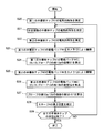
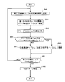
- FIG. 4 is a flowchart showing the semiconductor chip inspection method according to the first embodiment.
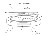
- FIG. 5 is a schematic diagram showing this semiconductor chip inspection method.
- FIG. 6 is a plan view of the wafer to be measured during the test of the first embodiment.
- FIG. 7 is a plan view showing an example of an appearance defect map created in the first embodiment.
- FIG. 8 is a schematic diagram of a test apparatus according to the second embodiment.
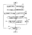
- FIG. 9 is a flowchart illustrating a semiconductor chip inspection method according to the third embodiment.
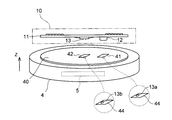
- FIG. 10 is a schematic diagram of a test apparatus according to the third embodiment.
- FIG. 11 is a plan view illustrating a method for calculating the amount of probe mark deviation in the third embodiment.
- FIG. 12 is a schematic plan view illustrating a method for calculating the rotation correction amount of the stage in the third embodiment.
- FIG. 13 is a flowchart illustrating a semiconductor chip inspection method according to the fourth embodiment.
- FIG. 14 is a schematic diagram of a test apparatus according to the fourth embodiment.
- FIG. 15A is an enlarged plan view of the electrode pad before correcting the height position of the stage in the fourth embodiment
- FIG. 15B is an enlarged plan view of the electrode pad after correction.
- FIG. 16 is a flowchart showing a semiconductor chip inspection method according to the fifth embodiment.
- FIG. 17A and 17B are schematic plan views showing the semiconductor chip inspection method according to the fourth embodiment.
- FIG. 18 is a flowchart showing a semiconductor chip inspection method according to the sixth embodiment.
- FIG. 19 is an enlarged plan view of an electrode pad during a test in the sixth embodiment.
- FIG. 20 is a flowchart illustrating a semiconductor chip inspection method according to the seventh embodiment.
- FIG. 21 is a plan view showing an example of an appearance defect map created in the seventh embodiment.
- FIG. 22 is a flowchart showing a semiconductor chip inspection method according to the eighth embodiment.
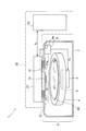
- FIG. 1 is a configuration diagram of a test apparatus according to the present embodiment.
- the test apparatus 1 has a prober 2 and a tester 20.
- the prober 2 includes a stage 4 on which the wafer 40 to be measured is mounted and a stage moving unit 3 that translates or rotates the stage 4 in a horizontal plane.
- the stage moving unit 3 also has a function of moving the stage 4 up and down in the vertical direction.
- Movement in elevation and the horizontal plane of the stage 4 is performed by an unillustrated stepping motor provided in the stage moving section 3, the lift amount and the amount of movement is controlled by a stage drive signal S m output from the control unit 9
- the stage 4 incorporates a temperature adjusting unit 5 for heating or cooling the wafer to be measured 40 to a predetermined temperature.
- a temperature adjusting unit 5 for heating or cooling the wafer to be measured 40 to a predetermined temperature.
- a resistance heating type heater may be provided as the temperature adjusting unit 5.
- a refrigerant pipe through which a refrigerant such as water flows may be provided as the temperature adjustment unit 5.
- a probe card 10 is provided above the stage 4 so as to face the wafer 40 to be measured.
- the probe card 10 includes a resin support substrate 11 having a peripheral edge fixed to the housing 7, and a plurality of probes 13 are attached to the support substrate 11.
- Each probe 13 is made of a thin metal wire such as tungsten, for example, and the interval between the probes 13 is secured by a resin layer 14 made of glass epoxy.
- a camera 12 for observing the wafer to be measured 40 is provided on the main surface of the support substrate 11 that faces the wafer to be measured 40.
- An image signal obtained by the camera 12 is taken into the control unit 9 via the cable 8.
- the control unit 9 is provided with a storage unit 9a such as a hard disk or RAM (Random Access Memory).
- the tester 20 includes a test head 21 and a test unit 22.
- Test unit 22 is electrically connected to the test head 21, and exchanges of the test signal S t between the test head 21.
- the test head 21 is attached to the housing 7 of the prober 2 so as to be openable and closable, and includes a conductive pin 23 that comes into contact with the electrode pad 11 a provided on the support substrate 11.
- the test signal St is supplied from the conductive pin 21 to the probe 13 via the electrode pad 11a.
- the stage 4 is driven in a horizontal plane so that the probe 13 is positioned above the first semiconductor chip 41 formed on the wafer 40 to be measured. Thereafter, by raising the stage 4, the prober 13 is applied to the electrode pad 44 of the first semiconductor chip 41, and the test signal St is supplied from the prober 13 to the first semiconductor chip 41.
- the camera 12 is positioned above the second semiconductor chip 42 different from the first semiconductor chip 41, and the second The electrode pads 44 of the semiconductor chip 42 can be observed.
- the magnification of the camera 12 is not particularly limited, but from the viewpoint that the state of the electrode pad 44 can be observed in detail, only one of the plurality of electrode pads 44 formed on the semiconductor chip 42 is within the field of view. It is preferable that the magnification is.
- the configuration of the present embodiment is not limited to the above, and the mounting position of the camera 12 may be modified to have a configuration as shown in FIG.
- FIG. 2 is a configuration diagram of a test apparatus according to a modification of the first embodiment.
- the same elements as those in FIG. 1 are denoted by the same reference numerals as those in FIG.
- the camera 12 is provided on the test head 21, and the opening 11 a is formed at a position corresponding to the camera 12 on the support substrate 11. With such a configuration, the wafer to be measured 40 is observed by the camera 12 through the opening 11a.
- FIG. 3 is a cross-sectional view of the wafer 40 to be measured.
- the wafer to be measured 40 has a multilayer wiring structure in which interlayer insulating films 43 such as silicon oxide films and metal wirings 45 such as aluminum wirings are alternately stacked on a silicon substrate 90.
- the film thickness is not particularly limited, but is preferably about 100 to 1000 ⁇ m for the interlayer insulating film 43 and about 100 to 2000 ⁇ m for the metal wiring 45.
- the passivation film 46 has a thickness of about 1 to 2 ⁇ m, for example, and includes an opening 46 a through which the surface of the electrode pad 44 is exposed.
- the planar shape of the electrode pads 44 is rectangular, and a plurality of electrodes are arranged in one chip at a pitch of about 40 to 50 ⁇ m.
- test apparatus 1 As the inspection method, either the test apparatus 1 shown in FIG. 1 or 2 may be used. The same applies to each embodiment described later.
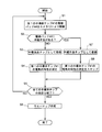
- FIG. 4 is a flowchart showing the semiconductor chip inspection method according to this embodiment.
- FIG. 5 is a schematic view showing the semiconductor chip inspection method
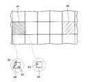
- FIG. 6 is a plan view of the wafer to be measured during the test.
- the camera is positioned at a position where the first semiconductor chip 41 can be observed when the second semiconductor chip 42 is measured prior to the unmeasured first semiconductor chip 41. 12 is provided.
- the electrode pad 44 of the first semiconductor chip 41 is observed by the camera 12 in the first step S1 of FIG.
- the observation timing is immediately after the probe 13 is retracted above the second semiconductor chip 42 and the test for the second semiconductor chip 42 is performed.
- electrode pads 44 to be observed are not particularly limited, and several representative ones of the plurality of electrode pads 44 formed on the semiconductor chip 41 may be observed, or only one electrode pad 44 may be observed. Also good.
- the image signal of the camera 12 obtained by observing the electrode pad 44 in this way is taken into the control unit 9 via the cable 8.
- step S2 in FIG. 4 the control unit 9 determines whether or not the electrode pad 44 of the first semiconductor chip 41 has an appearance defect based on the captured image signal.
- step S7 in FIG. 4 the process proceeds to step S7 in FIG. 4, and the first semiconductor chip 41 is registered as an appearance defect chip in the storage unit 9a (see FIG. 1).
- step S8 the process proceeds to step S8, and the measurement is skipped for the first semiconductor chip 41 registered as a defective appearance chip.
- step S2 determines whether there is no appearance defect (NO)
- the process proceeds to step S3, and the control unit 9 registers the first semiconductor chip 41 in the storage unit 9a as a good quality chip.
- step S4 the process proceeds to step S4, and after the measurement of a predetermined number of semiconductor chips, when the first semiconductor chip 41 moves below the probe 13, the stage 4 is raised under the control of the control unit 9. As a result, the probe 13 hits the electrode pad 44 of the first semiconductor chip 41 and the electrical characteristics of the first semiconductor chip 41 are measured.
- step S5 the control unit 9 determines whether or not the measurement of all the semiconductor chips formed on the wafer 40 to be measured has been completed.
- Step S1 is performed again on the semiconductor chip that has not been observed by the camera 12.
- step S6 create an appearance defect map. This step is performed by the measurement unit 9 based on the defective appearance chip and the good appearance chip registered in the storage unit 9a.
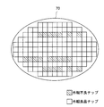
- FIG. 7 is a plan view showing an example of the appearance defect map 70.
- the appearance defect map 70 indicates the positions of the appearance defect chips and the good appearance chips on the wafer 40 to be measured.
- the measurement is skipped for the semiconductor chip 41 determined to be defective in step S8, the measurement is performed only for the semiconductor chip determined to be a good appearance.
- the first semiconductor chip 41 can be observed at the time of measurement of the second semiconductor chip 42 performed prior to the first semiconductor chip 41.
- a camera 12 is provided.
- the semiconductor chip is not measured using the probe 13, so that it is possible to prevent the probe 13 from being deformed by contact with a foreign substance or the like.
- FIG. 8 is a schematic diagram of a test apparatus according to a second embodiment.
- the same elements as those described in the first embodiment are denoted by the same reference numerals as those in the first embodiment, and the description thereof will be omitted below.
- the interval D between the probe 13 and the center of the field of view of the camera 12 is set to an integral multiple of the size S of each semiconductor chip (for example, the first semiconductor chip 41) formed on the wafer 40 to be measured.
- the electrode of the second semiconductor chip 42 is in the field of view of the camera 12 when the probe card 10 is retracted above the first semiconductor chip 41.
- the pad 44 can be accommodated. Therefore, it is not necessary to move the stage 4 in order to catch the electrode pad 44 by the camera 42, and the electrode pad 44 can be efficiently observed by omitting the moving time of the stage 4.
- the first and second measurements of the semiconductor chips 41 and 42 by the probe 13 are not limited, and the second semiconductor chip 42 before the measurement may be observed with the camera 12, or the second semiconductor chip 42 after the measurement may be observed. You may observe with the camera 12. FIG.
- FIG. 9 is a flowchart showing a semiconductor chip inspection method according to a third embodiment.
- FIG. 10 is a schematic diagram of a test apparatus according to the third embodiment.
- the same elements as those described in the first embodiment are denoted by the same reference numerals as those in the first embodiment, and the description thereof is omitted below.
- the camera 12 is provided at a position where the measured first semiconductor chip 41 can be observed when the second semiconductor chip 42 is measured after the first semiconductor chip 41. .
- the probe 13 is applied to the electrode pad 44 of the first semiconductor chip 41 by raising the stage 4 under the control of the control unit 9, so that the electrical connection of the first semiconductor chip 41 is performed. Measure characteristics.
- the electrode pad 44 of the first semiconductor chip 41 is marked with a mark 13 a by contact with the probe 13.
- step S11 the stage 4 is repeatedly raised and moved, and the electrical characteristics of a predetermined number of semiconductor chips between the first semiconductor chip 41 and the second semiconductor chip 42 are measured.
- step S12 the process proceeds to step S12, and under the control of the control unit 9, the probe 13 is applied to the electrode pad 44 of the second semiconductor chip 42 by the raising of the stage 4, and the electrical characteristics of the second semiconductor chip 42 are measured. As a result, the trace 13 b of the probe 13 is attached to the surface of the second semiconductor chip 42.
- the stage 4 is lowered. At this time, as shown in FIG. 10, the electrode pads 44 of the first semiconductor chip 41 are located below the camera 12.
- step S13 where the electrode pad 44 of the first semiconductor chip 41 below the camera 12 is observed, and the control unit 9 acquires the image data obtained thereby.
- the first semiconductor chip 41 is located below the camera 12, it is not necessary to move the stage 4 greatly in order to observe the electrode pads 44 of the semiconductor chip 41 with the camera.
- the state in which the probe 13 receives the radiant heat from the stage 4 can be maintained, it is possible to prevent the probe 13 from being deformed due to a temperature change when observing the electrode pad 44 and to waste time necessary for the movement of the stage 4. Can be omitted.
- electrode pads 44 to be observed are not particularly limited, and several representative pads among the plurality of electrode pads 44 formed on the first semiconductor chip 41 may be observed, or only one electrode pad 44 may be observed. You may observe.
- step S14 the control unit 9 grasps the position of the mark 13a of the probe 13 attached to the electrode pad 44 based on the image data acquired in step S13.
- the electrical characteristics of a predetermined number of semiconductor chips between the first semiconductor chip 41 and the second semiconductor chip 42 are measured by repeating the ascent and movement of the stage 4.
- step S15 the electrode pad 44 of the second semiconductor chip 42 that has moved below the camera 12 is observed by the camera 12, and the control unit 9 acquires the image data of the electrode pad 44.
- the second semiconductor chip 42 is located below the camera 12. Therefore, it is not necessary to largely move the stage 4 for observing the electrode pad 44.
- the electrode pad 44 can be observed while maintaining the state in which the probe 13 receives the radiant heat from the stage 4, and is necessary for the movement of the stage 4. Unnecessary time can be reduced.
- the electrode pads 44 to be observed are not particularly limited. However, when several representative electrode pads 44 in the first semiconductor chip 41 are observed in step S13, the same electrode pads 44 are also observed in this step. Like that.
- step S16 the controller 9 grasps the position of the mark 13b of the probe 13 attached to the electrode pad 44 of the second semiconductor chip 42 based on the image data of the electrode pad 44 acquired in step S15.
- step S17 the control unit 9 calculates the amount of displacement of each position of the marks 13a and 13b of the probe 13 acquired in step S14 and step S16.
- FIG. 11 is a plan view showing a method of calculating the amount of deviation.
- each semiconductor chip 41, 42 has n electrode pads 44, and an XY orthogonal coordinate system having two adjacent sides of each semiconductor chip 41, 42 as an X axis and a Y axis is used. It is arbitrarily set in the chip.
- the position coordinates of the center of the mark 13a attached to the i-th electrode pad 44 of the first semiconductor chip 41 are (X i (1) , Y i (1) ), and the i-th of the second semiconductor chip 42
- the position coordinates of the center of the mark 13b attached to the electrode pad 44 are (X i (2) , Y i (2) ).
- control unit 9 calculates the shift amount ( ⁇ X i , ⁇ Y i ) of the marks 13a and 13b in the i-th electrode pad 44 as in the following equation (1).
- step S18 in FIG. 9 the process proceeds to step S18 in FIG. 9, and the stage 4 is translated and rotated as follows to correct the position of the stage 4 in the horizontal plane.
- the average ( ⁇ X, ⁇ Y) of the deviation amounts in the n electrode pads 44 is expressed by the following equation (2) based on the above deviation amounts ( ⁇ X i , ⁇ Y i ).
- the control unit 9 calculates.
- stage 4 is translated in the horizontal plane by ( ⁇ X, ⁇ Y) where the sign of the average ( ⁇ X, ⁇ Y) of the deviation is reversed.
- Equation (2) instead of taking the average of the deviation amounts ( ⁇ X i , ⁇ Y i ) for all the n electrode pads 44 as shown in Equation (2), the calculation is performed by taking the average of several representative electrode pads 44. May be simplified.
- the electrode pad 44 in the corner portion of the semiconductor chips 41 and 42 is farthest from the center of the chip, the amount of deviation ( ⁇ X i , ⁇ Y i ) between the marks 13a and 13b tends to increase, and the representative electrode pad 44 Suitable as
- the present embodiment is not limited to this, and instead of taking the average of all the k electrode pads 44 as in the formulas (3) and (4), the representative electrode pads 44 out of the k electrode pads 44 are used. You may make it take the average about.
- FIG. 12 is a schematic plan view showing a method for calculating the rotation correction amount ⁇ of the stage 4 based on the deviation amounts ⁇ Y left and ⁇ Y right thus obtained.
- the length L is the distance between the centers of the left pad group 51 and the right pad group 52. Further, as shown by the solid line and the dotted line in the electrode pad 44, in this example, it is assumed that the trace of the probe 13 is shifted by the above-described average deviation amount ⁇ Y left and ⁇ Y right.
- the angle ⁇ can be calculated as in the following equation (5).
- the position of the stage 4 can be corrected by rotating the stage 4 by ⁇ under the control of the control unit 9.
- the stage 4 is corrected in a direction in which the average deviation amount ( ⁇ X, ⁇ Y) decreases.
- step S19 the control unit 9 determines whether or not the measurement of electrical characteristics has been completed for all the semiconductor chips formed on the wafer 40 to be measured.
- step S11 is performed again on the semiconductor chip whose electrical characteristics have not been completed.
- the probe 13 when the electrode pad 44 is observed in steps S13 and S15, the probe 13 is positioned above the stage 4, so that the probe 13 always receives radiant heat from the stage 4 during observation. Further, deformation of the probe 13 due to temperature change can be prevented.
- the shape of the probe 13 is not deformed when the electrode pad 44 is observed and when the semiconductor chips 41 and 42 are measured. This is because of the positional deviation between the marks 13a and 13b of the probe 13 attached to the electrode pad 44 during the measurement. Thermal deformation of the probe 13 can be eliminated.
- step S18 the positional deviation between the stage 4 and the probe 13 can be accurately corrected based on the rear 13a and 13b, and the positional deviation occurs between the electrode pad 44 and the probe 13 after the correction. Risk can be suppressed. As a result, it is possible to prevent the passivation film 46 from cracking due to the tip of the probe 13 coming into contact with the passivation film 46 around the electrode pad 44, and to maintain the reliability of the semiconductor chip.
- step S17 the trace 13a attached to the first semiconductor chip 41 that is initially measured in one wafer 40 to be measured is used as a measurement reference for the positional deviation of the trace of the probe 13. Therefore, even if the probe 13 is deformed by continuously measuring a plurality of semiconductor chips after the first semiconductor chip 41, the risk of missing a positional deviation between the electrode pad 44 and the probe 13 due to the deformation is reduced. .
- FIG. 13 is a flowchart showing a semiconductor chip inspection method according to this embodiment.
- FIG. 14 is a schematic diagram of a test apparatus according to the fourth embodiment.
- the same elements as those described in the first embodiment are denoted by the same reference numerals as those in the first embodiment, and the description thereof is omitted below.
- the camera 12 when measuring the second semiconductor chip 42 performed after the first semiconductor chip 41, the camera 12 is placed at a position where the measured first semiconductor chip 41 can be observed. Provide.
- the probe 13 is applied to the electrode pad 44 of the first semiconductor chip 41 by raising the stage 4 under the control of the control unit 9, and the electrical Measure characteristics.
- step S21 the raising and moving of the stage 4 are repeated, and the electrical characteristics of a predetermined number of semiconductor chips between the first semiconductor chip 41 and the second semiconductor chip 42 are measured.
- step S22 the stage 4 is raised under the control of the control unit 9, so that the probe 13 is applied to the electrode pad 44 of the second semiconductor chip 42, and the electrical characteristics of the second semiconductor chip 42 are measured. To do.
- the stage 4 is lowered. At this time, the electrode pads 44 of the first semiconductor chip 41 are located below the camera 12.
- step S23 the camera 12 observes the electrode pads 44 of the first semiconductor chip 41, and the control unit 9 acquires the image data obtained thereby.
- electrode pads 44 to be observed are not particularly limited, and several representative ones of the plurality of electrode pads 44 formed on the first semiconductor chip 41 may be observed. Alternatively, only one electrode pad 44 may be observed.
- step S24 the control unit 9 calculates the area S1 of the trace 13a of the probe 13 attached to the electrode pad 44 based on the image data acquired in step S23.
- the electrical characteristics of a predetermined number of semiconductor chips are measured by repeating the raising and moving of the stage 4.
- step S25 the electrode pad 44 of the second semiconductor chip 42 that has moved below the camera 12 is observed by the camera 12, and the control unit 9 acquires the image data of the electrode pad 44.
- the second semiconductor chip 42 is located below the camera 12, it is not necessary to move the stage 4 greatly for observing the electrode pad 44, and the probe 13 receives radiant heat from the stage 4.
- the electrode pad 44 can be observed while maintaining the state.
- electrode pads 44 to be observed are not particularly limited, but when several representative electrode pads 44 in the first semiconductor chip 41 are observed in step S23, the same electrode pads 44 are also observed in this step. Like that.
- step S26 the controller 9 calculates the area S2 of the trace 13b of the probe 13 attached to the electrode pad 44 of the second semiconductor chip 42 based on the image data of the electrode pad 44 acquired in step S25.
- step S27 the control unit 9 calculates a difference S2-S1 between the respective areas of the marks 13a and 13b of the probe 13 obtained in step S24 and step S26.
- the areas S1 and S2 of the marks 13a and 13b serve as a guide for the height position of the stage 4 at the time of measurement.
- the height position of the stage 4 is corrected so that the above-described area difference S2-S1 approaches zero.
- the correction is performed under the control of the control unit 9. For example, when the difference S2-S1 exceeds the positive specified value Smax , the stage 4 is lowered by a predetermined negative amount - ⁇ Z, and the difference S2- When S1 is smaller than the negative specified value ⁇ S min, the stage 4 is raised by a positive predetermined amount ⁇ Z.
- FIG. 15A is an enlarged plan view of the electrode pad 44 before the height position of the stage 4 is corrected
- FIG. 15B is an enlarged plan view of the electrode pad 44 after correction.
- the difference S2-S1 is obtained for each electrode pad 44, and the difference is calculated by averaging the number of the electrode pads 44 observed.
- Each specified value S max and ⁇ S min may be compared and corrected as described above.
- step S29 in FIG. 13 the control unit 9 determines whether or not the measurement of the electrical characteristics of all the semiconductor chips formed on the wafer 40 to be measured has been completed.
- step S21 is performed again on the semiconductor chip for which the measurement of electrical characteristics has not been completed.
- the stage 4 is used as described above by using the areas of the marks 13a and 13b of the probe 13 attached to the electrode pad 44. Can be corrected. Therefore, it is possible to prevent the probe 13 from being deformed due to excessive pressing on the electrode pad 44, or the contact force between the electrode pad 44 and the probe 13 is insufficient, and the electrical contact between them is insufficient. Can be prevented.
- the camera 12 when observing the electrode pad 44, the camera 12 is positioned above the chips 41 and 42, so that it is necessary to move the stage 4 for observation. There is no. This eliminates unnecessary time for moving the stage 4 and allows the probe 13 to always receive radiant heat from the stage 4 during observation, thereby preventing the probe 13 from being deformed due to temperature changes.
- FIG. 16 is a flowchart showing a semiconductor chip inspection method according to this embodiment.
- test apparatus The configuration of the test apparatus is the same as that in FIG. 10 described in the third embodiment, and will not be described below.
- FIGS. 17A and 17B are schematic plan views showing the semiconductor chip inspection method according to the present embodiment. 17A and 17B, the same elements as those described in the first embodiment are denoted by the same reference numerals as those in the first embodiment, and description thereof is omitted below.
- the electrical characteristics of a predetermined number of semiconductor chips are measured by repeatedly raising and moving the stage 4 under the control of the control unit 9.
- step S32 where the stage 4 is raised under the control of the control unit 9, so that the probe 13 is applied to the electrode pad 44 of the first semiconductor chip 41, and the electrical characteristics of the first semiconductor chip 41 are measured. To do.
- step S33 the electrode pad 44 of the first semiconductor chip 41 that has moved to the lower side of the camera 12 is observed by the camera 12, and the controller 9 causes the electrode pad 44 to be observed. Get image data.
- electrode pads 44 to be observed are not particularly limited, and only some representative ones of the plurality of electrode pads 44 formed on the semiconductor chip 41 may be observed. Alternatively, only one electrode pad 44 may be observed.
- the interval A between the trace 13a of the probe 13 attached to the electrode pad 44 and the contour of the electrode pad 44 is based on the prescribed value B, based on the above image data. Is determined by the control unit 9.
- the specified value B is not particularly limited, but is about 5 ⁇ m, for example.
- step S35 the position of the stage 4 is corrected in a direction in which the interval A becomes larger than the specified value B.
- the correction is performed by translating or rotating the stage 4 in the horizontal plane under the control of the control unit 9.
- the trace 13b of the probe 13 is the center of the electrode pad 44. You will be close.
- step S34 determines whether the value is larger than the specified value B (YES). If it is determined in step S34 that the value is larger than the specified value B (YES), the process proceeds to step S37 and the stage 4 is not corrected.
- step S36 the control unit 9 determines whether or not the measurement of the electrical characteristics has been completed for all the semiconductor chips formed on the wafer 40 to be measured.
- step S31 is performed again on the semiconductor chip for which measurement of electrical characteristics has not been completed.
- the stage 4 is corrected to correct the distance A. Is larger than the specified value B.
- the stage 4 can be corrected before the contact position reaches the contour of the electrode pad 44. Therefore, the risk that the probe 13 comes off from the electrode pad 44 and hits the passivation film 46 is reduced, and it is possible to prevent the passivation film 46 from being cracked by contact with the probe 13.
- step S33 when observing the electrode pad 44 with the camera 12 in step S33, since the camera 12 is above the first semiconductor chip 41, it is not necessary to move the stage 4 for observation. Therefore, the time for movement is not required, the state in which the probe 13 receives the radiant heat from the stage 4 can be maintained, and the probe 13 can be prevented from being deformed due to a temperature change.
- FIG. 18 is a flowchart showing a semiconductor chip inspection method according to this embodiment.
- test apparatus The configuration of the test apparatus is the same as that in FIG. 10 described in the third embodiment, and will not be described below.
- FIG. 19 is an enlarged plan view of the electrode pad 44 during the test in the present embodiment.
- the electrical characteristics of the first semiconductor chip 41 which is one of the plurality of semiconductor chips of the wafer 40 to be measured, are measured.
- step S41 the electrode pads 40 of the first semiconductor chip 41 are observed with the camera 12. .
- the image signal obtained by this observation is taken into the control unit 9.
- the electrode pads 44 observed in this step are not particularly limited, and only a representative number of the electrode pads 44 formed on the semiconductor chip 41 may be observed, or only one electrode pad 44 may be observed. May be observed.
- step S42 the control unit 9 grasps the position of the mark 13a (see FIG. 19) of the probe 13 based on the image signal output from the camera 12.
- step S43 the controller 9 determines whether or not the mark 13a protrudes from the electrode pad 44 as shown in FIG.
- step S45 the control unit 9 determines to stop the measurement of another semiconductor chip performed after the measurement of the first semiconductor chip 41.
- step S44 the control unit 9 determines whether or not the measurement of the electrical characteristics of all the semiconductor chips formed on the wafer 40 to be measured has been completed. To do.
- step S40 is performed again on the semiconductor chip for which the measurement of electrical characteristics has not been completed.
- step S43 when it is determined in step S43 that the trace 13a of the probe 13 protrudes from the electrode pad 44, the process proceeds to step S45 and the subsequent measurement is stopped.
- the probe 13 As a cause of the protrusion 13a protruding from the electrode pad 44, for example, there is a case where the probe 13 is excessively deformed due to stepping on a foreign matter on the electrode pad 44. In this case, the position of the stage 4 is corrected only by the electrode pad. The probe 13 cannot be applied to 44.
- the deformed probe 13 can be prevented from coming off from the electrode pad 44 of the subsequent semiconductor chip and hitting the passivation film 46, and the semiconductor is caused by scratches on the passivation film 46. It can suppress that the yield of a chip
- FIG. 20 is a flowchart showing a semiconductor chip inspection method according to this embodiment.
- This embodiment is the same as the sixth embodiment in steps S40 to S43, but the steps performed after the determination in step S43 are different from the sixth embodiment as follows.
- step S43 determines in step S43 that the mark 13a does not protrude from the electrode pad 44 (NO)
- the process proceeds to step S50, and the controller 9 stores the first semiconductor chip 40 in the storage unit 9a ( (See Fig. 1).
- step S43 determines in step S43 that the mark 13a protrudes from the electrode pad 44 (YES)
- the process proceeds to step S53, and the control unit 9 puts the first semiconductor chip 40 in the storage unit 9a. Register as a defective chip.
- step S51 the control unit 9 determines whether or not the measurement of all the semiconductor chips formed on the wafer to be measured 40 has been completed.
- step S40 is performed again on the semiconductor chip for which the measurement of the electrical characteristics has not been completed.
- step S52 create an appearance defect map. This step is performed by the measurement unit 9 based on the defective appearance chip and the good appearance chip registered in the storage unit 9a.
- FIG. 21 is a plan view showing an example of the appearance defect map 80.
- the appearance defect map 80 shows the positions of the appearance defect chips and the appearance good chips on the wafer 40 to be measured.
- a defective appearance chip and a good appearance chip are discriminated.
- an appearance inspection process for inspecting the appearance of each semiconductor chip becomes unnecessary, which can contribute to shortening the manufacturing process of the semiconductor device.
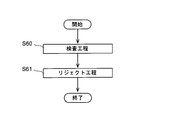
- FIG. 22 is a flowchart showing the semiconductor chip inspection method according to the present embodiment.
- the electrical characteristics of each semiconductor chip are inspected for the wafer 40 to be measured provided with a plurality of semiconductor chips. Then, the electrode pad 44 is observed by the camera 12 as described in the first to seventh embodiments with respect to the semiconductor chip to be inspected.
- the process proceeds to the reject process S61, and only the semiconductor chips determined to be non-defective are left except for the semiconductor chips determined to be defective in the inspection of the electrical characteristics in the inspection process S60.
Landscapes
- Engineering & Computer Science (AREA)
- Computer Hardware Design (AREA)
- Microelectronics & Electronic Packaging (AREA)
- General Engineering & Computer Science (AREA)
- Physics & Mathematics (AREA)
- General Physics & Mathematics (AREA)
- Testing Or Measuring Of Semiconductors Or The Like (AREA)
- Tests Of Electronic Circuits (AREA)
Abstract
【課題】プローバ、試験装置、及び半導体チップの検査方法において、ステージを大きく移動させなくても電極パッドを観察できるようにすること。 【解決手段】支持基板11と、支持基板11に取り付けられたプローブ13とを備えるプローブカード10と、被測定ウエハ40を載せるステージ4と、プローブカード10上に設けられ、被測定ウエハ40に形成された第1の半導体チップ41の電極パッド44を観測するカメラ12と、プローブカード10に対するステージ4の位置を移動させるステージ移動部3とを有するプローバ2による。
Description
本発明は、プローバ、試験装置、及び半導体チップの検査方法に関する。
LSI等の半導体装置の製造工程では、ウエハに回路を形成した後、その回路が所定の動作をするかどうかを確認するための電気的な試験が行われる。
その試験では、例えば、製品の温度保証範囲で回路が動作するかどうかを確認するために、加熱又は冷却されたステージ上にウエハを載せ、ウエハに集積形成された半導体チップに試験装置のプローブが当てられる。
試験を正常に行うには、そのプローブは、半導体チップの電極パッドに正確に当てられるべきである。
ところが、上記のようにステージを加熱又は冷却すると、ステージからの輻射熱によってプローブが変形し、その先端が電極パッドから外れてしまうことがある。その場合、電極パッド周囲のパッシベーション膜にプローブの先端が接触し、パッシベーション膜にプローブ痕が付いてしまう。また、最悪の場合には、パッシベーション膜にクラックが発生し、半導体装置において電源間リーク等の不具合が発生することもある。
特に、システムLSIのように外部接続端子の縮小化や狭ピッチ化が顕著な半導体装置では、上記したようなプローブの位置ずれが発生し易く、改善が求められる。
そのようなプローブの位置ずれを防止する方法として、例えば、所定個数のチップの試験が終了する度に、プローブカードの下方からカメラによりプローブを観察する方法がある。この場合、カメラによる観察でプローブの先端の位置を認識し、位置ずれが相殺されるような方向にステージを移動させることになる。
しかし、この方法では、プローブをカメラで認識するために、ステージをプローバから一旦退避させる必要があり、退避のための余計な時間が必要となる。しかも、ステージがプローバから退避している最中にプローブが自然冷却してしまうので、その間にプローブが変形し、プローブの先端の位置を正確に測れないという問題もある。
更に、この方法では、プローブと電極パッドとの位置ずれによりパッシベーション膜にプローブ痕が付いているかどうかを試験中に確認できず、試験後の外観検査工程においてプローブ痕を発見することになる。しかし、これでは、ステージ位置を正確に補正できなかった場合に、プローブ痕に起因した不良が連続した複数のチップに発生する恐れがあり、最悪の場合には一枚のウエハの全てのチップが不良になることもある。
その他の方法として、プローブと電極パッドとの位置決めを行うために、ステージをプロカードから一旦退避させ、プローブとの接触によって電極パッドについたプローブ痕を認識する方法もある。
しかし、この方法でも、ステージの退避を伴うため、自然冷却によるプローブの変形と退避のための試験時間の長期化が避けられない。更に、この方法は、プローブ痕が電極パッドについたのか、或いはプローブが電極パッドから外れたのかを判定するだけであり、電極パッドにプローブが当たればよい程度の位置決めしかできず、電極パッドとプローブとを高精度に位置合わせするのが難しい。
また、電極パッドに付いたプローブ痕の位置をカメラによって認識し、それにより電極パッドからプローブ痕がはみ出していることが分かった場合には警報を出して測定を停止させたり、プローブと電極パッドとの再位置決めを行ったりする方法もある。
しかしながら、この方法では、プローブ痕をカメラで認識するときに、カメラのある所までステージを搬送する必要があるので、搬送のための余計な時間が必要であると共に、搬送の間にプローブが自然冷却して変形するという既述の問題が解決できない。
特開昭60-24030号公報
特開昭59-5641号公報
特公平7-13990号公報
特開平7-147304号公報
特開2008-108930号公報
プローバ、試験装置、及び半導体チップの検査方法において、ステージを大きく移動させなくても電極パッドを観察できるようにすることを目的とする。
以下の開示の一観点によれば、支持基板と、前記支持基板に取り付けられたプローブとを備えるプローブカードと、被測定ウエハを載せるステージと、前記プローブカード上に設けられ、前記被測定ウエハに形成された第1の半導体チップの電極パッドを観測するカメラと、前記プローブカードに対する前記ステージの位置を移動させる移動手段とを有するプローバが提供される。
また、その開示の別の観点によれば、テスタ部と、前記テスタ部と電気的に接続されるプローバ部とを有し、前記プローバ部は、支持基板と、前記支持基板に取り付けられたプローブとを備えるプローブカードと、被測定ウエハを載せるステージと、前記プローブカード上に設けられ、前記被測定ウエハに形成された半導体チップの電極パッドを観測するカメラと、前記プローブカードに対する前記ステージの位置を移動させる移動手段とを有する試験装置が開示される。
更に、その開示の他の観点によれば、プローブカードの支持基板に取り付けられたプローブを、ステージ上の被測定ウエハに形成された第1の半導体チップの電極パッドに接触させ、前記第1の半導体チップの電気的特性を測定するステップを有し、前記第1の半導体チップの測定前若しくは測定後に、前記支持基板上或いは前記プローブカードの上方に設けられたカメラによって、前記第1の半導体チップの電極パッドを観察する半導体チップの検査方法が開示される。
(1)第1実施形態
図1は、本実施形態に係る試験装置の構成図である。
図1は、本実施形態に係る試験装置の構成図である。
この試験装置1は、プローバ2とテスタ20とを有する。
このうち、プローバ2は、被測定ウエハ40を載せるステージ4と、そのステージ4を水平面内で並進若しくは回転させるステージ移動部3とを筐体7内に備える。なお、そのステージ移動部3は、ステージ4を鉛直方向に昇降させる機能も有する。
ステージ4の昇降や水平面内での移動は、ステージ移動部3に設けられた不図示のステッピングモータによって行われ、昇降量や移動量は制御部9から出力されるステージ駆動信号Smによって制御される。
また、ステージ4には、被測定ウエハ40を所定の温度に加熱又は冷却するための温度調節部5が内蔵される。被測定ウエハ40を加熱するには、例えば抵抗加熱型のヒータを温度調節部5として設ければよい。一方、被測定ウエハ40を冷却するには、水等の冷媒が流れる冷媒配管を温度調節部5として設ければよい。
更に、ステージ4の上方には、被測定ウエハ40と対向するようにしてプローブカード10が設けられる。
プローブカード10は、周縁部が筐体7に固定された樹脂製の支持基板11を備えており、その支持基板11には複数本のプローブ13が取り付けられる。各プローブ13は、例えばタングステン等の金属細線よりなり、ガラスエポキシよりなる樹脂層14によって各プローブ13の間隔が確保される。
そして、支持基板11において被測定ウエハ40と対向する主面には、被測定ウエハ40を観察するためのカメラ12が設けられる。そのカメラ12で得られた画像信号は、ケーブル8を介して制御部9に取り込まれる。また、その制御部9には、ハードディスクやRAM(Random Access Memory)等の記憶部9aが設けられる。
一方、テスタ20は、テストヘッド21と試験部22とを有する。
試験部22は、テストヘッド21に電気的に接続され、テストヘッド21との間で試験信号Stの授受を行う。
また、テストヘッド21は、プローバ2の筐体7に開閉可能に取り付けられており、支持基板11に設けられた電極パッド11aに当接する導電ピン23を備える。被測定ウエハ40に対して検査を行う際には、その導電ピン21から電極パッド11aを介してプローブ13に試験信号Stが供給されることになる。
検査に際しては、被測定ウエハ40に形成された第1の半導体チップ41の上方にプローブ13が位置するようにステージ4を水平面内で駆動する。その後、ステージ4を上昇させることにより、第1の半導体チップ41の電極パッド44にプローバ13を当て、プローバ13から第1の半導体チップ41に試験信号Stを供給する。
このようにプローバ13が第1の半導体チップ41の上方に位置しているとき、カメラ12は、第1の半導体チップ41とは別の第2の半導体チップ42の上方に位置し、第2の半導体チップ42の電極パッド44を観察できるようになっている。
カメラ12の倍率は特に限定されないが、電極パッド44の状態を詳細に観察できるとうい観点からすると、半導体チップ42に形成された複数の電極パッド44のうちの一つのみが視野内に入る程度の倍率であるのが好ましい。
なお、本実施形態の構成は上記に限定されず、カメラ12の取り付け位置を変形し、図2のような構成としてもよい。
図2は、第1実施形態の変形例に係る試験装置の構成図である。なお、図2において図1と同じ要素には図1と同じ符号を付し、以下ではその説明を省略する。
図2の例では、テストヘッド21にカメラ12を設けると共に、支持基板11においてカメラ12に対応する位置に開口11aを形成する。このような構成とすることで、カメラ12により開口11aを通じて被測定ウエハ40が観察されることになる。
図3は、被測定ウエハ40の断面図である。
その被測定ウエハ40は、シリコン基板90の上に、酸化シリコン膜等の層間絶縁膜43とアルミニウム配線等の金属配線45とを交互に積層してなる多層配線構造を有する。これらの膜厚は特に限定されないが、層間絶縁膜43については100~1000μm程度、金属配線45については100~2000μm程度とするのが好ましい。
そして、最上層の層間絶縁膜43の上には、アルミニウム膜等の金属膜をパターニングしてなる0.4~2μm程度の厚さの電極パッド44と、窒化シリコン膜やポリイミド膜等のパッシベーション膜46が形成される。そのパッシベーション膜46は、例えば1~2μm程度の厚さを有すると共に、電極パッド44の表面が露出する開口46aを備える。
また、電極パッド44の平面形状は矩形状であり、40~50μm程度のピッチで1チップ内に複数配列される。
次に、この試験装置1を用いた半導体チップの検査方法について説明する。なお、その検査方法は、図1と図2のどちらの試験装置1を用いてもよい。これについては後述の各実施形態でも同様である。
図4は、本実施形態に係る半導体チップの検査方法について示すフローチャートである。また、図5は、この半導体チップの検査方法について示す模式図であり、図6は試験時における被測定ウエハの平面図である。
図5に示されるように、本実施形態では、未測定の第1の半導体チップ41に先行して行われる第2の半導体チップ42の測定時に、第1の半導体チップ41を観察できる位置にカメラ12を設ける。
そして、図4の最初のステップS1では、上記の第1の半導体チップ41の電極パッド44をカメラ12により観察する。観察するタイミングは、第2の半導体チップ42の上方にプローブ13が退避しており、第2の半導体チップ42に対する試験を行った直後である。
また、観察する電極パッド44は特に限定されず、半導体チップ41に形成された複数の電極パッド44のうち、代表の数個を観察してもよいし、一つの電極パッド44のみを観察してもよい。
このように電極パッド44を観察して得られたカメラ12の画像信号は、ケーブル8を介して制御部9に取り込まれる。
そして、図4のステップS2に移り、取り込まれた画像信号に基づき、制御部9が第1の半導体チップ41の電極パッド44に外観不良があるかどうかを判断する。
そのような外観不良としては、図6に示すように、電極パッド44に付着した異物61や、表面傷62等がある。
ここで、外観不良がある(YES)と判断された場合には、図4のステップS7に移り、記憶部9a(図1参照)に第1の半導体チップ41を外観不良チップとして登録する。
そして、ステップS8に移り、外観不良チップとして登録された第1の半導体チップ41については測定をスキップするようにする。
一方、ステップS2において外観不良がない(NO)と判断された場合には、ステップS3に移り、制御部9が記憶部9aに第1の半導体チップ41を外観良品チップとして登録する。
そして、ステップS4に移り、所定個数の半導体チップの測定の後に第1の半導体チップ41がプローブ13の下方に移動してきたところで、制御部9の制御下でステージ4を上昇させる。これにより、第1の半導体チップ41の電極パッド44にプローブ13が当たり、第1の半導体チップ41の電気的特性が測定される。
次いで、ステップS5に移り、被測定ウエハ40に形成されている全ての半導体チップの測定が終了したかどうかを制御部9が判断する。
ここで、終了していない(NO)と判断された場合には、カメラ12による観察が終わっていない半導体チップに対し、ステップS1を再び行う。
一方、終了した(YES)と判断された場合には、ステップS6に移り、外観不良マップを作成する。本ステップは、記憶部9aに登録された外観不良チップと外観良品チップに基づいて測定部9が行う。
図7は、この外観不良マップ70の一例を示す平面図である。
外観不良マップ70は、被測定ウエハ40における外観不良チップと外観良品チップの位置を示すものである。
本実施形態では、ステップS8において外観不良と判断された半導体チップ41に対しては測定をスキップするので、外観良品と判断された半導体チップに対してのみ測定が行われることになる。
以上により、本実施形態に係る半導体チップの検査方法の主要ステップを終了する。
上記した本実施形態によれば、図5に示したように、第1の半導体チップ41に先行して行われる第2の半導体チップ42の測定時に、第1の半導体チップ41を観察できる位置にカメラ12を設けるようにした。
そのため、カメラ12により第1の半導体チップ41を観察するためにステージ4を大きく移動させる必要がないので、ステージ4の移動のための無駄な時間を削減できる。
更に、このように第2の半導体チップ42の測定に並行して第1の半導体チップ41の外観を観察するので、被測定ウエハ40に対する電気的な測定を行う工程と、外観を観察する工程とを同時に行うことができ、半導体装置の製造工程の短縮化に寄与できる。
しかも、観察によって外観不良があると判ったら、その半導体チップに対してはプローブ13を用いた測定を行わないので、異物等との接触でプローブ13が変形するのを未然に防止できる。
(2)第2実施形態
図8は、第2実施形態に係る試験装置の模式図である。なお、図7において、第1実施形態で説明したのと同じ要素には第1実施形態と同じ符号を付し、以下ではその説明を省略する。
図8は、第2実施形態に係る試験装置の模式図である。なお、図7において、第1実施形態で説明したのと同じ要素には第1実施形態と同じ符号を付し、以下ではその説明を省略する。
本実施形態では、プローブ13とカメラ12の視野中心との間隔Dを、被測定ウエハ40に形成されている各半導体チップ(例えば、第1の半導体チップ41)のサイズSの整数倍とする。
このようにすると、第1の半導体チップ41の測定の直後において、第1の半導体チップ41の上方にプローブカード10が退避しているときに、カメラ12の視野に第2の半導体チップ42の電極パッド44が収まるようになる。よって、カメラ42によって電極パッド44を捉えるためにステージ4を移動させる必要がなく、ステージ4の移動時間を省略して効率的に電極パッド44を観察することができる。
なお、プローブ13による各半導体チップ41、42の測定の先後は限定されず、測定前の第2の半導体チップ42をカメラ12で観察してもよいし、測定後の第2の半導体チップ42をカメラ12で観察してもよい。
(3)第3実施形態
図9は、第3実施形態に係る半導体チップの検査方法について示すフローチャートである。
図9は、第3実施形態に係る半導体チップの検査方法について示すフローチャートである。
また、図10は、第3実施形態に係る試験装置の模式図である。なお、図10において、第1実施形態で説明したのと同じ要素には第1実施形態と同じ符号を付し、以下ではその説明を省略する。
本実施形態では、図10に示すように、第1の半導体チップ41の後に行われる第2の半導体チップ42の測定時に、測定済みの第1の半導体チップ41を観察できる位置にカメラ12を設ける。
そして、図9の最初のステップS10では、制御部9の制御下でステージ4を上昇させることにより第1の半導体チップ41の電極パッド44にプローブ13を当て、第1の半導体チップ41の電気的特性を測定する。
このとき、第1の半導体チップ41の電極パッド44には、プローブ13との接触によって痕13aが付く。
次いで、ステップS11に移り、ステージ4の上昇と移動とを繰り返し、第1の半導体チップ41と第2の半導体チップ42の間にある所定個数の半導体チップの電気的特性を測定する。
その後、ステップS12に移り、制御部9の制御下において、ステージ4の上昇により第2の半導体チップ42の電極パッド44にプローブ13を当て、第2の半導体チップ42の電気的特性を測定する。これにより、第2の半導体チップ42の表面には、プローブ13の痕13bが付くことになる。
そして、測定が終了したらステージ4を下降させる。このとき、図10に示すように、カメラ12の下方には第1の半導体チップ41の電極パッド44が位置している。
次いで、ステップS13に移り、カメラ12の下方にある第1の半導体チップ41の電極パッド44を観察し、これにより得られた画像データを制御部9が取得する。
ここで、第1の半導体チップ41はカメラ12の下方に位置しているので、半導体チップ41の電極パッド44をカメラで観察するためにステージ4を大きく移動させる必要がない。
そのため、プローブ13がステージ4からの輻射熱を受けている状態を維持できるので、電極パッド44の観察時に温度変化によってプローブ13が変形するのを防止できると共に、ステージ4の移動に必要な無駄な時間を省くこともできる。
なお、観察する電極パッド44は特に限定されず、第1の半導体チップ41に形成された複数の電極パッド44のうち、代表の数個を観察してもよいし、一つの電極パッド44のみを観察してもよい。
そして、ステップS14に移り、ステップS13で取得した画像データを元にして、制御部9が電極パッド44についたプローブ13の痕13aの位置を把握する。
その後、ステージ4の上昇と移動とを繰り返すことにより、第1の半導体チップ41と第2の半導体チップ42の間にある所定個数の半導体チップの電気的特性を測定する。
そして、ステップS15に移り、カメラ12の下方に移動してきた第2の半導体チップ42の電極パッド44をカメラ12により観察し、制御部9が該電極パッド44の画像データを取得する。
このとき、第2の半導体チップ42はカメラ12の下方に位置している。そのため、電極パッド44の観察のためにステージ4を大きく移動させる必要がない。
したがって、ステップS13で第1の半導体チップ41を観察したときと同様に、ステージ4からの輻射熱をプローブ13が受けている状態を維持しながら電極パッド44を観察できると共に、ステージ4の移動に必要な無駄な時間も削減できる。
また、観察する電極パッド44は特に限定されないが、ステップS13において第1の半導体チップ41における代表の数個の電極パッド44を観察した場合には、本ステップでもそれらと同じ電極パッド44を観察するようにする。
次いで、ステップS16に移り、ステップS15で取得した電極パッド44の画像データに基づき、第2の半導体チップ42の電極パッド44に付いたプローブ13の痕13bの位置を制御部9が把握する。
その後、ステップS17に移り、ステップS14とステップS16で取得したプローブ13の痕13a、13bのそれぞれの位置のズレ量を制御部9が算出する。
図11は、そのズレ量の算出方法について示す平面図である。
この例では、各半導体チップ41、42にn個の電極パッド44がある場合を想定しており、各半導体チップ41、42の隣接する二辺をX軸、Y軸とするX-Y直交座標系をチップ内に任意に設定している。
そして、第1の半導体チップ41のi番目の電極パッド44に付いた痕13aの中心の位置座標を(Xi
(1)、Yi
(1))とし、第2の半導体チップ42のi番目の電極パッド44に付いた痕13bの中心の位置座標を(Xi
(2)、Yi
(2))としている。
この場合、i番目の電極パッド44おける痕13a、13bのズレ量(ΔXi, ΔYi)を、次の式(1)のようにして制御部9が算出する。

次いで、図9のステップS18に移り、以下のようにしてステージ4を並進及び回転させ、水平面内でのステージ4の位置を補正する。
まず、並進による補正については、上記のズレ量(ΔXi, ΔYi)に基づいて、n個の電極パッド44におけるズレ量の平均(ΔX, ΔY)を次の式(2)のようにして制御部9が算出する。

そして、制御部9の制御下で、このズレ量の平均(ΔX, ΔY)の符号を逆にした(-ΔX,-ΔY)だけステージ4を水平面内で並進させる。
なお、式(2)のようにn個の全ての電極パッド44についてズレ量(ΔXi, ΔYi)の平均を取るのではなく、数個の代表の電極パッド44についての平均を取り、計算を簡略化してもよい。
例えば、半導体チップ41、42のコーナ部における電極パッド44は、チップの中心から最も離れているので、痕13a、13bのズレ量(ΔXi, ΔYi)が大きくなり易く、代表の電極パッド44として適している。
一方、回転による補正については、図11に示した電極パッド44の並びのうち、対向するパッド群51、52にのみ注目する。そして、左側のパッド群51と右側のパッド群52のそれぞれについて、プローブの痕13a、13bのY方向の平均のズレ量ΔY左、ΔY右を次のようにして算出する。


なお、式(3)、(4)においては、左側のパッド群51には添え字がpから始まる電極パッド44が全部でk個ある場合を想定し、右側のパッド群52には添え字がqから始まる電極パッド44が全部でk個ある場合を想定している。
但し、本実施形態はこれに限定されず、式(3)、(4)のようにk個の全ての電極パッド44についての平均を取るのではなく、k個のなかから代表の電極パッド44についての平均を取るようにしてもよい。
図12は、このように求めたズレ量ΔY左、ΔY右に基づいたステージ4の回転補正量Δθの算出方法について示す模式平面図である。
なお、図12において、長さLは、左側のパッド群51と右側のパッド群52のそれぞれの中心間距離である。また、電極パッド44内で実線と点線で示すように、この例ではプローブ13の痕が上記した平均のズレ量ΔY左、ΔY右だけずれている場合を想定している。
図12に示されるように、電極パッド44とプローバ13とが全体的に角度Δθだけ回転ずれを起こしていると、角度Δθの正接は、(ΔY左+ΔY右)/Lと近似できる。
よって、次の式(5)のように角度Δθを算出し得る。

このように算出した角度Δθに基づき、制御部9の制御下においてステージ4を-Δθだけ回転させることにより、ステージ4の位置補正を行うことができる。
上記のようにして水平面内においてステージ4を並進及び回転させることにより、本ステップでは、ズレ量の平均(ΔX, ΔY)が小さくなる方向にステージ4が補正されることになる。
次に、図9のステップS19に移る。
そのステップS19では、被測定ウエハ40に形成されている全ての半導体チップについて電気的特性の測定が終了したかどうかを制御部9が判断する。
そして、終了していない(NO)と判断した場合には、電気的特性の終了していない半導体チップに対してステップS11を再び行う。
一方、終了した(YES)と判断した場合には、この被測定ウエハ40の測定を終了し、次の被測定ウエハの受け入れの準備をする。
以上により、本実施形態に係る半導体チップの検査方法の主要ステップが終了した。
上記した本実施形態では、ステップS13、S15において電極パッド44を観察するとき、プローブ13はステージ4の上方に位置しているので、観察中にプローブ13はステージ4からの輻射熱を常に受けており、温度変化に伴うプローブ13の変形を防止できる。
したがって、電極パッド44の観察時と各半導体チップ41、42の測定時とでプローブ13の形状が変形せず、測定時に電極パッド44に付くプローブ13の痕13a、13b同士の位置ずれの要因からプローブ13の熱変形を排除できる。
そのため、ステップS18において、これらの後13a、13bに基づいてステージ4とプローブ13との位置ずれを正確に補正できるようになり、補正後に電極パッド44とプローブ13との間に位置ずれが発生する危険性を抑制できる。その結果、電極パッド44周囲のパッシベーション膜46にプローブ13の先端が接触することが原因でパッシベーション膜46にクラックが生じるのを防止でき、半導体チップの信頼性を維持することが可能となる。
更に、ステップS17では、プローブ13の痕の位置ずれの計測基準として、1枚の被測定ウエハ40のうち初期に測定される第1の半導体チップ41についた痕13aを用いる。そのため、第1の半導体チップ41の後に複数の半導体チップを連続して測定したことでプローブ13が変形しても、その変形に伴う電極パッド44とプローブ13との位置ずれを見逃す危険性が減る。
(4)第4実施形態
図13は、本実施形態に係る半導体チップの検査方法について示すフローチャートである。
図13は、本実施形態に係る半導体チップの検査方法について示すフローチャートである。
また、図14は、第4実施形態に係る試験装置の模式図である。なお、図14において、第1実施形態で説明したのと同じ要素には第1実施形態と同じ符号を付し、以下ではその説明を省略する。
本実施形態でも、第3実施形態と同様に、第1の半導体チップ41の後に行われる第2の半導体チップ42の測定時に、測定済みの第1の半導体チップ41を観察できる位置にカメラ12を設ける。
そして、図13の最初のステップS20では、制御部9の制御下でステージ4を上昇させることにより第1の半導体チップ41の電極パッド44にプローブ13を当て、第1の半導体チップ41の電気的特性を測定する。
このようにプローブ13を当てたことで、電極パッド44にはプローブ13の痕13aが付くことになる。
次いで、ステップS21に移り、ステージ4の上昇と移動とを繰り返し、第1の半導体チップ41と第2の半導体チップ42の間の所定個数の半導体チップの電気的特性を測定する。
その後、ステップS22に移り、制御部9の制御下においてステージ4を上昇させることにより、第2の半導体チップ42の電極パッド44にプローブ13を当て、第2の半導体チップ42の電気的特性を測定する。そして、測定が終了したらステージ4を下降させる。このとき、カメラ12の下方には第1の半導体チップ41の電極パッド44が位置している。
次いで、ステップS23に移り、カメラ12により第1の半導体チップ41の電極パッド44を観察し、これにより得られた画像データを制御部9が取得する。
なお、観察する電極パッド44は特に限定されず、第1の半導体チップ41に形成された複数の電極パッド44のうち、代表の数個を観察するようにしてもよい。或いは、一つの電極パッド44のみを観察してもよい。
そして、ステップS24に移り、ステップS23で取得した画像データを元にして、制御部9が電極パッド44についたプローブ13の痕13aの面積S1を算出する。
その後、ステージ4の上昇と移動とを繰り返すことにより、所定個数の半導体チップの電気的特性を測定する。
そして、ステップS25に移り、カメラ12の下方に移動してきた第2の半導体チップ42の電極パッド44をカメラ12により観察し、制御部9が該電極パッド44の画像データを取得する。
このとき、第2の半導体チップ42はカメラ12の下方に位置しているため、電極パッド44の観察のためにステージ4を大きく移動させる必要がないうえ、ステージ4からの輻射熱をプローブ13が受けている状態を維持しながら電極パッド44を観察できる。
また、観察する電極パッド44は特に限定されないが、ステップS23において第1の半導体チップ41における代表の数個の電極パッド44を観察した場合には、本ステップでもそれらと同じ電極パッド44を観察するようにする。
次いで、ステップS26に移り、ステップS25で取得した電極パッド44の画像データに基づき、第2の半導体チップ42の電極パッド44に付いたプローブ13の痕13bの面積S2を制御部9が算出する。
その後、ステップS27に移り、ステップS24とステップS26で取得したプローブ13の痕13a、13bのそれぞれの面積の差S2-S1を制御部9が算出する。
ここで、痕13a、13bの面積S1、S2は、測定時におけるステージ4の高さ位置の目安となり、その面積が大きいほどステージ4の位置が高くプローブ13が電極パッド44に強く押し当てられていることになる。
したがって、ステップS24とS26の間において、経時変化等によってプローブ13の高さが変動していなければ、時間間隔をおいて測定された各面積S1、S2の差S2-S1は0になるはずである。
これに対し、差S2-S1が0でない場合には、経時変化等によってプローブ13の高さが変動していると推定できる。
そこで、次のステップS28では、上記の面積の差S2-S1が0に近づく方向にステージ4の高さ位置を補正する。
その補正は、制御部9の制御下において行われ、例えば、差S2-S1が正の規定値Smaxを超えている場合には負の所定量-ΔZだけステージ4を下降させ、差S2-S1が負の規定値-Sminよりも小さい場合には正の所定量ΔZだけステージ4を上昇させて行われる。
図15(a)は、ステージ4の高さ位置を補正する前の電極パッド44の拡大平面図であり、図15(b)は、補正後の電極パッド44の拡大平面図である。
この例では、補正前(図15(a))に電極パッド44に付いたプローブ13の痕13aが、補正によってステージ4の高さ位置を上昇させたことで、補正後(図15(b))ではその面積が増大している。
なお、ステップS23、S25で複数個の電極パッド44を観察した場合には、個々の電極パッド44について差S2-S1を求め、それらを観察した電極パッド44の個数で平均し、当該平均値と各規定値Smax、-Sminとを比較して上記のように補正してもよい。
次に、図13のステップS29に移り、被測定ウエハ40に形成されている全ての半導体チップについて電気的特性の測定が終了したかどうかを制御部9が判断する。
そして、終了していない(NO)と判断した場合には、電気的特性の測定が終了していない半導体チップに対してステップS21を再び行う。
一方、終了した(YES)と判断した場合には、この被測定ウエハ40の測定を終了し、次の被測定ウエハの受け入れの準備をする。
以上により、本実施形態に係る半導体チップの検査方法の主要ステップが終了した。
上記した本実施形態によれば、経時変化等によってプローブ13の高さが変動した場合でも、電極パッド44に付いたプローブ13の痕13a、13bの面積を利用することにより上記のようにステージ4の高さを補正できる。そのため、電極パッド44への過度な押し付けが原因でプローブ13が変形するのを防止したり、電極パッド44とプローブ13との接触力が不足してこれらの間の電気的なコンタクトが不十分になるのを防止したりできる。
しかも、第3実施形態と同様に、本実施形態でも電極パッド44を観察する際には各チップ41、42の上方にカメラ12が位置しているので、観察のためにステージ4を移動させる必要がない。これにより、ステージ4の移動のための無駄な時間が不要になると共に、観察時にステージ4からの輻射熱をプローブ13が常に受けることができ、温度変化によってプローブ13が変形するのを防止できる。
(5)第5実施形態
図16は、本実施形態に係る半導体チップの検査方法について示すフローチャートである。
図16は、本実施形態に係る半導体チップの検査方法について示すフローチャートである。
なお、試験装置の構成については、第3実施形態で説明した図10におけるのと同様なので、以下では省略する。
また、図17(a)、(b)は、本実施形態に係る半導体チップの検査方法について示す模式平面図である。図17(a)、(b)において、第1実施形態で説明したのと同じ要素には第1実施形態と同じ符号を付し、以下ではその説明を省略する。
図16の最初のステップS31では、制御部9の制御下においてステージ4の上昇と移動とを繰り返すことにより、所定個数の半導体チップの電気的特性を測定する。
次いで、ステップS32に移り、制御部9の制御下においてステージ4を上昇させることで、第1の半導体チップ41の電極パッド44にプローブ13を当て、第1の半導体チップ41の電気的特性を測定する。
そして、所定個数の半導体チップを測定した後、ステップS33に移り、カメラ12の下方に移動してきた第1の半導体チップ41の電極パッド44をカメラ12により観察し、制御部9が該電極パッド44の画像データを取得する。
なお、観察する電極パッド44は特に限定されず、半導体チップ41に形成された複数の電極パッド44のうち、代表の数個のみを観察してもよい。或いは、一つの電極パッド44のみを観察してもよい。
次に、ステップS34に移る。
本ステップでは、図17(a)に示すように、上記の画像データを基にして、電極パッド44に付いたプローブ13の痕13aと電極パッド44の輪郭との間隔Aが、規定値Bよりも大きいかどうかを制御部9が判断する。
その規定値Bは特に限定されないが、例えば5μm程度である。
そして、規定値Bよりも大きくない(NO)と判断した場合には、ステップS35に移り、間隔Aが規定値Bよりも大きくなる方向にステージ4の位置を補正する。その補正は、制御部9の制御下で水平面内においてステージ4を並進又は回転させることにより行われる。
このような補正の結果、図17(b)に示すように、第1の半導体チップ41の測定後に行われる第2の半導体チップ42の測定においては、プローブ13の痕13bが電極パッド44の中央寄りに付くことになる。
一方、ステップS34において規定値Bよりも大きい(YES)と判断した場合には、ステップS37に移り、ステージ4の補正をしないこととする。
その後、ステップS36に移り、被測定ウエハ40に形成されている全ての半導体チップについて電気的特性の測定が終了したかどうかを制御部9が判断する。
そして、終了していない(NO)と判断した場合には、電気的特性の測定が終了していない半導体チップに対してステップS31を再び行う。
一方、終了した(YES)と判断した場合には、この被測定ウエハ40の測定を終了し、次の被測定ウエハの受け入れの準備をする。
以上により、本実施形態に係る半導体チップの検査方法の主要ステップが終了した。
上記した本実施形態によれば、図17(a)に示したように、電極パッド44の輪郭と痕13aとの間隔Aが規定値Bよりも小さい場合に、ステージ4を補正して間隔Aが規定値Bよりも大きくなるようにする。
これにより、経時変化によってプローブ13と電極パッド44との接触位置が電極パッド44の中心から次第にずれる場合でも、当該接触位置が電極パッド44の輪郭に達する前にステージ4を補正できる。そのため、プローブ13が電極パッド44から外れてパッシベーション膜46に当たる危険性が減り、プローブ13との接触でパッシベーション膜46にクラックが入るのを防止できる。
更に、ステップS33においてカメラ12により電極パッド44を観察するときには、第1の半導体チップ41の上方にカメラ12があるので、観察のためにステージ4を大きく移動する必要がない。よって、移動のための時間が不要であると共に、ステージ4からの輻射熱をプローブ13が受けた状態を維持でき、温度変化によってプローブ13が変形するのを防止できる。
(6)第6実施形態
図18は、本実施形態に係る半導体チップの検査方法について示すフローチャートである。
図18は、本実施形態に係る半導体チップの検査方法について示すフローチャートである。
なお、試験装置の構成については、第3実施形態で説明した図10におけるのと同様なので、以下では省略する。
また、図19は、本実施形態における試験時の電極パッド44の拡大平面図である。
図18の最初のステップS40では、制御部9の制御下において、被測定ウエハ40の複数の半導体チップの中の一つである第1の半導体チップ41の電気的特性を測定する。
その後、所定個数の半導体チップ40の測定を行い、カメラ12の下方に第1の半導体チップ41が移動してきたところでステップS41に移り、第1の半導体チップ41の電極パッド40をカメラ12で観察する。この観察により得られた画像信号は、制御部9に取り込まれる。
また、本ステップにおいて観察する電極パッド44は特に限定されず、半導体チップ41に形成された複数の電極パッド44のうち、代表の数個のみを観察してもよいし、一つの電極パッド44のみを観察してもよい。
次に、ステップS42に移り、カメラ12から出力された画像信号に基づき、制御部9がプローブ13の痕13a(図19参照)の位置を把握する。
そして、ステップS43に移り、図19のように痕13aが電極パッド44からはみ出しているかどうかの判断を制御部9が行う。
そして、はみ出している(YES)と判断した場合には、ステップS45に移り、第1の半導体チップ41の測定後に行われる他の半導体チップの測定の中止を制御部9が決定する。
一方、はみ出していない(NO)と判断した場合には、ステップS44に移り、被測定ウエハ40に形成されている全ての半導体チップについて電気的特性の測定が終了したかどうかを制御部9が判断する。
そして、終了していない(NO)と判断した場合には、電気特性の測定が終わっていない半導体チップに対してステップS40を再び行う。
一方、終了した(YES)と判断した場合には、この被測定ウエハ40の測定を終了し、次の被測定ウエハの受け入れの準備をする。
以上により、本実施形態に係る半導体チップの検査方法の主要ステップが終了した。
上記した本実施形態によれば、ステップS43においてプローブ13の痕13aが電極パッド44からはみ出していると判断した場合には、ステップS45に移ってそれ以降の測定を中止する。
痕13aが電極パッド44からはみ出る原因としては、例えば、電極パッド44上の異物を踏んだことが原因でプローブ13が過度に変形した場合があり、その場合はステージ4の位置補正だけでは電極パッド44にプローブ13を当てることができなくなる。
そのような場合に、上記のように測定を中止すれば、変形したプローブ13が後続の半導体チップの電極パッド44から外れてパッシベーション膜46に当たるのを防止でき、パッシベーション膜46の傷が原因で半導体チップの歩留まりが低下するのを抑制できる。
(7)第7実施形態
図20は、本実施形態に係る半導体チップの検査方法について示すフローチャートである。
図20は、本実施形態に係る半導体チップの検査方法について示すフローチャートである。
本実施形態は、ステップS40~S43までは第6実施形態と同一であるが、ステップS43での判断以降に行われるステップが以下のように第6実施形態とは異なる。
まず、ステップS43において制御部9により痕13aが電極パッド44からはみ出していない(NO)と判断された場合には、ステップS50に移り、制御部9が第1の半導体チップ40を記憶部9a(図1参照)に外観良品チップとして登録する。
一方、ステップS43において制御部9により痕13aが電極パッド44からはみ出している(YES)と判断された場合には、ステップS53に移り、制御部9が第1の半導体チップ40を記憶部9aに外観不良チップとして登録する。
続いて、ステップS51に移り、制御部9が被測定ウエハ40に形成されている全ての半導体チップの測定が終了したかどうかを判断する。
ここで、終了していない(NO)と判断された場合には、電気特性の測定が終わっていない半導体チップに対してステップS40を再び行う。
一方、終了した(YES)と判断された場合には、ステップS52に移り、外観不良マップを作成する。本ステップは、記憶部9aに登録された外観不良チップと外観良品チップに基づいて測定部9が行う。
図21は、この外観不良マップ80の一例を示す平面図である。
外観不良マップ80は、被測定ウエハ40における外観不良チップと外観良品チップの位置を示すものである。
以上により、本実施形態に係る半導体チップの検査方法の主要ステップが終了した。
上記した本実施形態によれば、被測定ウエハ40に形成されている複数の半導体チップの測定と並行して、ステップS50、S53において外観不良チップと外観良品チップの判別を行う。
そのため、被測定ウエハ40の電気的特性の測定を行った後、各半導体チップの外観を検査する外観検査工程が不要になり、半導体装置の製造工程の短縮化に寄与することができる。
(8)第8実施形態
本実施形態では、半導体チップの実際の量産工程への第1~第7実施形態の適用方法について説明する。
本実施形態では、半導体チップの実際の量産工程への第1~第7実施形態の適用方法について説明する。
図22は、本実施形態に係る半導体チップの検査方法について示すフローチャートである。
本実施形態では、図22の検査工程S60において、複数の半導体チップが設けられた被測定ウエハ40に対し、各半導体チップの電気的特性を検査する。そして、その検査の対象となる半導体チップに対し、第1~第7実施形態で説明したようなカメラ12による電極パッド44の観察を行う。
次いで、リジェクト工程S61に移り、検査工程S60における電気的特性の検査で不良と判断された半導体チップを除いて、良品と判断された半導体チップのみを残すようにする。
以上により、本実施形態に係る半導体チップの検査方法の主要ステップを終了する。
本実施形態のように量産工程に第1~第7実施形態を適用することで、電極パッド44の観察時におけるプローバ13の熱変形を防止できる等の効果を実際の量産工程で得ることができる。
Claims (19)
- 支持基板と、前記支持基板に取り付けられたプローブとを備えるプローブカードと、
被測定ウエハを載せるステージと、
前記プローブカード上に設けられ、前記被測定ウエハに形成された第1の半導体チップの電極パッドを観測するカメラと、
前記プローブカードに対する前記ステージの位置を移動させる移動手段と、
を有することを特徴とするプローバ。 - 前記カメラの画像信号の取り込みと、前記移動手段の制御とを行う制御部を更に有し、
前記制御部が、
前記カメラの画像信号に基づき、前記第1の半導体チップの前記電極パッドに付いた前記プローブの痕の位置を把握し、
前記第1の半導体チップの測定の後に、前記ステージ上の前記被測定ウエハに形成された第2の半導体チップの電極パッドに前記プローブを接触させ、前記第2の半導体チップの電気的特性を測定し
前記第2の半導体チップの測定後に、前記カメラによって前記第2の半導体チップの電極パッドを観察し、
前記カメラの画像信号に基づき、前記第2の半導体チップの前記電極パッドに付いた前記プローブの痕の位置を把握し、
前記第1の半導体チップの前記電極パッドについた前記プローブの痕の位置と、前記第2の半導体チップの前記電極パッドについた前記プローブの痕の位置とのズレ量を計測し、
前記ズレ量が小さくなる方向に前記ステージの位置を補正することを特徴とする請求項1に記載のプローバ。 - 前記制御部は、
前記カメラの画像信号に基づき、前記プローブの痕と前記電極パッドの輪郭との間隔が規定値よりも大きいかどうかを判断し、
前記間隔が前記規定値よりも大きくないと判断したときに、前記間隔が前記規定値よりも大きくなる方向に前記ステージの位置を補正することを特徴とする請求項1に記載のプローバ。 - 前記制御部は、
前記カメラの画像信号に基づき、前記第1の半導体チップの前記電極パッドに付いた前記プローブの痕の位置を把握し
前記把握されたプローブの痕の位置に基づいて、前記痕が前記電極パッドからはみ出しているかどうかを判断し、
前記痕が前記電極パッドからはみ出していると判断された場合に、前記第1の半導体チップの測定後に行われる他の半導体チップの測定の中止を決定することを特徴とする請求項1に記載のプローバ。 - 前記制御部は、
前記カメラの画像信号に基づき、前記第1の半導体チップの前記電極パッドに付いた前記プローブの痕の位置を把握し、
前記把握されたプローブの痕の位置に基づいて、前記痕が前記電極パッドからはみ出しているかどうかを判断し、
前記痕が前記電極パッドからはみ出していると判断した場合に、前記第1の半導体チップを外観不良チップとして記憶し、
前記痕が前記電極パッドからはみ出していないと判断した場合に、前記第1の半導体チップを外観良品チップとして記憶し、
前記記憶した前記外観不良チップと前記外観良品チップの前記被測定ウエハ内での位置を示すウエハマップを作成することを特徴とする請求項1に記載のプローバ。 - 前記制御部は、
前記カメラの画像信号に基づき、前記第1の半導体チップの前記電極パッドに付いた前記プローブの痕の面積を算出し、
前記第1の半導体チップの測定の後に、前記ステージ上の前記被測定ウエハに形成された第2の半導体チップの電極パッドに前記プローブを接触させ、前記第2の半導体チップの電気的特性を測定し、
前記第2の半導体チップの測定後に、前記カメラによって前記第2の半導体チップの電極パッドを観察し、
前記カメラによる前記観察の結果に基づき、前記第2の半導体チップの前記電極パッドに付いた前記プローブの痕の面積を算出し、
前記第1の半導体チップの前記電極パッドについた前記プローブの痕の面積と、前記第2の半導体チップの前記電極パッドについた前記プローブの痕の面積との差を計測し、
前記差が0に近づく方向に前記ステージの高さ位置を補正することを特徴とする請求項1に記載のプローバ。 - 前記制御部は、
前記第1の半導体チップの測定の前に、前記カメラの前記画像信号に基づき、前記電極パッドに外観不良があるかどうかを判断し、
前記電極パッドに外観不良があると判断した場合に、前記第1の半導体チップを外観不良チップとして記憶し、
前記電極パッドに外観不良がないと判断した場合に、前記第1の半導体チップを外観良品チップとして記憶し、
前記記憶した前記外観不良チップと前記外観良品チップの前記被測定ウエハ内での位置を示すウエハマップを作成することを特徴とする請求項1に記載のプローバ。 - 前記プローブと前記カメラの視野中心との間隔は、前記第1の半導体チップのサイズの整数倍であることを特徴とする請求項1に記載のプローバ。
- テスタ部と、
前記テスタ部と電気的に接続されるプローバ部とを有し、
前記プローバ部は、
支持基板と、前記支持基板に取り付けられたプローブとを備えるプローブカードと、
被測定ウエハを載せるステージと、
前記プローブカード上に設けられ、前記被測定ウエハに形成された半導体チップの電極パッドを観測するカメラと、
前記プローブカードに対する前記ステージの位置を移動させる移動手段と、
を有することを特徴とする試験装置。 - 前記テスタ部は、前記プローブカードに当接するテストヘッドを備え、
前記カメラが前記テストヘッド上に設けられ、且つ、前記支持基板において前記カメラに対応する位置に開口が設けられていることを特徴とする請求項9に記載の試験装置。 - プローブカードの支持基板に取り付けられたプローブを、ステージ上の被測定ウエハに形成された第1の半導体チップの電極パッドに接触させ、前記第1の半導体チップの電気的特性を測定するステップを有し、
前記第1の半導体チップの測定前若しくは測定後に、前記支持基板上或いは前記プローブカードの上方に設けられたカメラによって、前記第1の半導体チップの電極パッドを観察することを特徴とする半導体チップの検査方法。 - 前記カメラによる前記観察の結果に基づき、前記第1の半導体チップの前記電極パッドに付いた前記プローブの痕の位置を把握するステップと、
前記第1の半導体チップの測定の後に、前記ステージ上の前記被測定ウエハに形成された第2の半導体チップの電極パッドに前記プローブを接触させ、前記第2の半導体チップの電気的特性を測定するステップと、
前記第2の半導体チップの測定後に、前記カメラによって前記第2の半導体チップの電極パッドを観察するステップと、
前記カメラによる前記観察の結果に基づき、前記第2の半導体チップの前記電極パッドに付いた前記プローブの痕の位置を把握するステップと、
前記第1の半導体チップの前記電極パッドについた前記プローブの痕の位置と、前記第2の半導体チップの前記電極パッドについた前記プローブの痕の位置とのズレ量を計測するステップと、
前記ズレ量が小さくなる方向に前記ステージの位置を補正するステップとを更に有することを特徴とする請求項11に記載の半導体チップの検査方法。 - 前記ステージの位置を補正するステップにおいて、水平面内で前記ステージを並進若しくは回転することにより、前記ステージの位置を補正することを特徴とする請求項12に記載の半導体チップの検査方法。
- 前記カメラによる前記観察の結果に基づき、前記プローブの痕と前記電極パッドの輪郭との間隔が規定値よりも大きいかどうかを判断するステップと、
前記間隔が前記規定値よりも大きくないと判断されたときに、前記間隔が前記規定値よりも大きくなる方向に前記ステージの位置を補正するステップとを更に有することを特徴とする請求項11に記載の半導体チップの検査方法。 - 前記カメラによる前記観察の結果に基づき、前記第1の半導体チップの前記電極パッドに付いた前記プローブの痕の位置を把握するステップと、
前記把握されたプローブの痕の位置に基づいて、前記痕が前記電極パッドからはみ出しているかどうかを判断するステップと、
前記痕が前記電極パッドからはみ出していると判断された場合に、前記第1の半導体チップの測定後に行われる他の半導体チップの測定の中止を決定するステップとを更に有することを特徴とする請求項11に記載の半導体チップの検査方法。 - 前記カメラによる前記観察の結果に基づき、前記第1の半導体チップの前記電極パッドに付いた前記プローブの痕の位置を把握するステップと、
前記把握されたプローブの痕の位置に基づいて、前記痕が前記電極パッドからはみ出しているかどうかを判断するステップと、
前記痕が前記電極パッドからはみ出していると判断した場合に、前記第1の半導体チップを外観不良チップとして記憶するステップと、
前記痕が前記電極パッドからはみ出していないと判断した場合に、前記第1の半導体チップを外観良品チップとして記憶するステップと、
前記記憶した前記外観不良チップと前記外観良品チップの前記被測定ウエハ内での位置を示すウエハマップを作成するステップとを更に有することを特徴とする請求項11に記載の半導体チップの検査方法。 - 前記カメラによる前記観察の結果に基づき、前記第1の半導体チップの前記電極パッドに付いた前記プローブの痕の面積を把握するステップと、
前記第1の半導体チップの測定の後に、前記ステージ上の前記被測定ウエハに形成された第2の半導体チップの電極パッドに前記プローブを接触させ、前記第2の半導体チップの電気的特性を測定するステップと、
前記第2の半導体チップの測定後に、前記カメラによって前記第2の半導体チップの電極パッドを観察するステップと、
前記カメラによる前記観察の結果に基づき、前記第2の半導体チップの前記電極パッドに付いた前記プローブの痕の面積を把握するステップと、
前記第1の半導体チップの前記電極パッドについた前記プローブの痕の面積と、前記第2の半導体チップの前記電極パッドについた前記プローブの痕の面積との差を計測するステップと、
前記差が0に近づく方向に前記ステージの高さ位置を補正するステップとを更に有することを特徴とする請求項11に記載の半導体チップの検査方法。 - 前記第1の半導体チップの測定の前に、前記カメラによる前記観察の結果に基づき、前記電極パッドに外観不良があるかどうかを判断するステップと、
前記電極パッドに外観不良があると判断した場合に、前記第1の半導体チップを外観不良チップとして記憶するステップと、
前記電極パッドに外観不良がないと判断した場合に、前記第1の半導体チップを外観良品チップとして記憶するステップと
前記記憶した前記外観不良チップと前記外観良品チップの前記被測定ウエハ内での位置を示すウエハマップを作成するステップとを更に有することを特徴とする請求項11に記載の半導体チップの検査方法。 - 複数の半導体チップが設けられた前記被測定ウエハに対し、前記半導体チップの電気的特性を検査する検査工程と、
前記検査の結果、不良と判断された前記半導体チップを除いて、良品と判断された前記半導体チップのみを製品として残す工程とを更に有し、
前記第1の半導体チップは前記複数の半導体チップの一つであり、
前記第1の半導体チップの電気的特性を測定するステップと、前記電極パッドを観察するステップは、前記検査工程において行われることを特徴とする請求項11に記載の半導体チップの検査方法。
Priority Applications (3)
| Application Number | Priority Date | Filing Date | Title |
|---|---|---|---|
| PCT/JP2008/073707 WO2010073359A1 (ja) | 2008-12-26 | 2008-12-26 | プローバ、試験装置、及び半導体チップの検査方法 |
| JP2010543694A JP5370370B2 (ja) | 2008-12-26 | 2008-12-26 | プローバ、試験装置、及び半導体チップの検査方法 |
| US13/168,719 US8797055B2 (en) | 2008-12-26 | 2011-06-24 | Prober and method of inspecting semiconductor chip |
Applications Claiming Priority (1)
| Application Number | Priority Date | Filing Date | Title |
|---|---|---|---|
| PCT/JP2008/073707 WO2010073359A1 (ja) | 2008-12-26 | 2008-12-26 | プローバ、試験装置、及び半導体チップの検査方法 |
Related Child Applications (1)
| Application Number | Title | Priority Date | Filing Date |
|---|---|---|---|
| US13/168,719 Continuation US8797055B2 (en) | 2008-12-26 | 2011-06-24 | Prober and method of inspecting semiconductor chip |
Publications (1)
| Publication Number | Publication Date |
|---|---|
| WO2010073359A1 true WO2010073359A1 (ja) | 2010-07-01 |
Family
ID=42287027
Family Applications (1)
| Application Number | Title | Priority Date | Filing Date |
|---|---|---|---|
| PCT/JP2008/073707 Ceased WO2010073359A1 (ja) | 2008-12-26 | 2008-12-26 | プローバ、試験装置、及び半導体チップの検査方法 |
Country Status (3)
| Country | Link |
|---|---|
| US (1) | US8797055B2 (ja) |
| JP (1) | JP5370370B2 (ja) |
| WO (1) | WO2010073359A1 (ja) |
Cited By (2)
| Publication number | Priority date | Publication date | Assignee | Title |
|---|---|---|---|---|
| KR101397242B1 (ko) * | 2013-03-27 | 2014-05-20 | 세메스 주식회사 | 웨이퍼를 테스트하는 방법 및 장치 |
| WO2015033744A1 (ja) * | 2013-09-06 | 2015-03-12 | ヤマハファインテック株式会社 | 電気検査装置 |
Families Citing this family (18)
| Publication number | Priority date | Publication date | Assignee | Title |
|---|---|---|---|---|
| US8476918B2 (en) * | 2010-04-28 | 2013-07-02 | Tsmc Solid State Lighting Ltd. | Apparatus and method for wafer level classification of light emitting device |
| US9000798B2 (en) * | 2012-06-13 | 2015-04-07 | Taiwan Semiconductor Manufacturing Company, Ltd. | Method of test probe alignment control |
| JP2014115115A (ja) * | 2012-12-06 | 2014-06-26 | Advantest Corp | 補正装置、プローブ装置、および試験装置 |
| JP6999321B2 (ja) * | 2017-07-31 | 2022-01-18 | 東京エレクトロン株式会社 | 検査装置、検査方法及び記憶媒体 |
| KR20190041678A (ko) * | 2017-10-13 | 2019-04-23 | 삼성전자주식회사 | 반도체 칩 검사 장치 |
| JP6955989B2 (ja) * | 2017-12-13 | 2021-10-27 | 東京エレクトロン株式会社 | 検査装置 |
| CN111025072B (zh) * | 2019-12-31 | 2025-03-25 | 湘能华磊光电股份有限公司 | 一种芯片光电性能及外观检测装置 |
| US11486899B2 (en) * | 2020-01-31 | 2022-11-01 | Nanya Technology Corporation | Wafer test system and methods thereof |
| US11532524B2 (en) | 2020-07-27 | 2022-12-20 | Taiwan Semiconductor Manufacturing Co., Ltd. | Integrated circuit test method and structure thereof |
| JP7829278B2 (ja) * | 2020-12-09 | 2026-03-13 | 東京エレクトロン株式会社 | 電源および検査装置 |
| TWI790515B (zh) * | 2020-12-21 | 2023-01-21 | 矽品精密工業股份有限公司 | 測試裝置及測試方法 |
| CN113075233B (zh) * | 2021-04-12 | 2025-01-24 | 长春光华微电子设备工程中心有限公司 | 一种探针台针痕检测方法 |
| TWI794990B (zh) * | 2021-09-23 | 2023-03-01 | 牧德科技股份有限公司 | 電測治具扎針位置估算方法 |
| KR102917872B1 (ko) | 2021-10-06 | 2026-01-28 | 삼성전자주식회사 | 전기적 테스트를 예측하는 컴퓨팅 장치, 및 그것을 갖는 전기적 테스트 예측 장치 및 그것의 동작 방법 |
| US12211200B2 (en) | 2022-04-19 | 2025-01-28 | Nanya Technology Corporation | Wafer inspection system method |
| TWI809928B (zh) * | 2022-04-19 | 2023-07-21 | 南亞科技股份有限公司 | 晶圓檢測系統 |
| US12148144B2 (en) | 2022-04-19 | 2024-11-19 | Nanya Technology Corporation | Wafer inspection system |
| CN120507548B (zh) * | 2025-07-21 | 2025-11-28 | 矽电半导体设备(深圳)股份有限公司 | 探针台及测试系统 |
Citations (2)
| Publication number | Priority date | Publication date | Assignee | Title |
|---|---|---|---|---|
| JP2003068813A (ja) * | 2001-08-23 | 2003-03-07 | Dainippon Screen Mfg Co Ltd | プローブ痕測定方法およびプローブ痕測定装置 |
| JP2007095766A (ja) * | 2005-09-27 | 2007-04-12 | Fujifilm Corp | プローバ装置及び半導体デバイスの検査方法 |
Family Cites Families (11)
| Publication number | Priority date | Publication date | Assignee | Title |
|---|---|---|---|---|
| JPS595641A (ja) | 1982-07-02 | 1984-01-12 | Hitachi Ltd | プロ−バ |
| JPS6024030A (ja) | 1983-07-19 | 1985-02-06 | Telmec Co Ltd | 半導体ウエハ測定方法 |
| JPH0713990B2 (ja) | 1985-04-02 | 1995-02-15 | 東京エレクトロン株式会社 | プローブ針とパッドの位置合わせ方法 |
| US5644245A (en) | 1993-11-24 | 1997-07-01 | Tokyo Electron Limited | Probe apparatus for inspecting electrical characteristics of a microelectronic element |
| JPH07147304A (ja) | 1993-11-24 | 1995-06-06 | Tokyo Electron Ltd | オートセットアップ式プローブ検査方法 |
| US7026832B2 (en) * | 2002-10-28 | 2006-04-11 | Dainippon Screen Mfg. Co., Ltd. | Probe mark reading device and probe mark reading method |
| JP2006049599A (ja) * | 2004-08-05 | 2006-02-16 | Seiko Epson Corp | ウェハプローバ及び半導体装置の製造方法、半導体試験装置 |
| JP2007183194A (ja) * | 2006-01-10 | 2007-07-19 | Micronics Japan Co Ltd | プロービング装置 |
| JP2008108930A (ja) | 2006-10-26 | 2008-05-08 | Matsushita Electric Ind Co Ltd | 半導体装置の検査方法およびプローブカード |
| JP5018183B2 (ja) * | 2007-03-30 | 2012-09-05 | 東京エレクトロン株式会社 | プローブ装置、プロービング方法及び記憶媒体 |
| JP5322822B2 (ja) * | 2009-07-27 | 2013-10-23 | 株式会社日本マイクロニクス | 半導体検査用ウエハプローバ及び検査方法 |
-
2008
- 2008-12-26 WO PCT/JP2008/073707 patent/WO2010073359A1/ja not_active Ceased
- 2008-12-26 JP JP2010543694A patent/JP5370370B2/ja not_active Expired - Fee Related
-
2011
- 2011-06-24 US US13/168,719 patent/US8797055B2/en not_active Expired - Fee Related
Patent Citations (2)
| Publication number | Priority date | Publication date | Assignee | Title |
|---|---|---|---|---|
| JP2003068813A (ja) * | 2001-08-23 | 2003-03-07 | Dainippon Screen Mfg Co Ltd | プローブ痕測定方法およびプローブ痕測定装置 |
| JP2007095766A (ja) * | 2005-09-27 | 2007-04-12 | Fujifilm Corp | プローバ装置及び半導体デバイスの検査方法 |
Cited By (3)
| Publication number | Priority date | Publication date | Assignee | Title |
|---|---|---|---|---|
| KR101397242B1 (ko) * | 2013-03-27 | 2014-05-20 | 세메스 주식회사 | 웨이퍼를 테스트하는 방법 및 장치 |
| WO2015033744A1 (ja) * | 2013-09-06 | 2015-03-12 | ヤマハファインテック株式会社 | 電気検査装置 |
| JP2015052511A (ja) * | 2013-09-06 | 2015-03-19 | ヤマハファインテック株式会社 | 電気検査装置 |
Also Published As
| Publication number | Publication date |
|---|---|
| US20110254574A1 (en) | 2011-10-20 |
| JP5370370B2 (ja) | 2013-12-18 |
| US8797055B2 (en) | 2014-08-05 |
| JPWO2010073359A1 (ja) | 2012-05-31 |
Similar Documents
| Publication | Publication Date | Title |
|---|---|---|
| JP5370370B2 (ja) | プローバ、試験装置、及び半導体チップの検査方法 | |
| JP4357813B2 (ja) | プローブ装置及びプローブ方法 | |
| TWI236723B (en) | Probe sheet, probe card, semiconductor inspection device, and manufacturing method for semiconductor device | |
| JP4187718B2 (ja) | プローブカード | |
| US5172053A (en) | Prober apparatus | |
| JP4997127B2 (ja) | 検査方法及びこの検査方法を記録したプログラム記録媒体 | |
| US20060114008A1 (en) | Probe card for testing semiconductor element, and semiconductor device tested by the same | |
| US20100301884A1 (en) | Thin-film probe sheet and method of manufacturing the same, probe card, and semiconductor chip inspection apparatus | |
| US7626406B2 (en) | Probing method, probe apparatus and storage medium | |
| TWI402932B (zh) | 具有多軸載台之半導體元件測試裝置 | |
| JP3800394B2 (ja) | プローブカード解析及びスクラブマーク解析データを最適化するための方法 | |
| KR20100101451A (ko) | 반도체 디바이스 테스트 장치 및 방법 | |
| KR20190106708A (ko) | 위치 보정 방법, 검사 장치 및 프로브 카드 | |
| JP5529605B2 (ja) | ウエハチャックの傾き補正方法及びプローブ装置 | |
| JP2737744B2 (ja) | ウエハプロービング装置 | |
| JP2986142B2 (ja) | プローブ方法 | |
| JP7176284B2 (ja) | プローブ装置、プローブの検査方法、及び記憶媒体 | |
| JP3248136B1 (ja) | プローブ方法及びプローブ装置 | |
| JP4391738B2 (ja) | プローブの接触位置の採取方法、プローブの接触位置の補正方法及びプローブ装置間の接触誤差の解消方法 | |
| JP2008028103A (ja) | ウエハプローバ | |
| US12613270B2 (en) | Wafer acceptance test tool and test method using thereof | |
| JP2022096153A (ja) | 電子デバイスの検査装置及び検査方法 | |
| JP2006177787A (ja) | 針圧調整用プローブカード、プローブ針の針圧調整方法および半導体装置の特性検査方法 | |
| JP3103959B2 (ja) | プローブ装置 | |
| JP2003344478A (ja) | 検査装置及び検査方法 |
Legal Events
| Date | Code | Title | Description |
|---|---|---|---|
| 121 | Ep: the epo has been informed by wipo that ep was designated in this application |
Ref document number: 08879155 Country of ref document: EP Kind code of ref document: A1 |
|
| WWE | Wipo information: entry into national phase |
Ref document number: 2010543694 Country of ref document: JP |
|
| NENP | Non-entry into the national phase |
Ref country code: DE |
|
| 122 | Ep: pct application non-entry in european phase |
Ref document number: 08879155 Country of ref document: EP Kind code of ref document: A1 |